KR20090016813A - Manufacturing method of semiconductor device - Google Patents
Manufacturing method of semiconductor deviceDownload PDFInfo
- Publication number
- KR20090016813A KR20090016813AKR1020070081074AKR20070081074AKR20090016813AKR 20090016813 AKR20090016813 AKR 20090016813AKR 1020070081074 AKR1020070081074 AKR 1020070081074AKR 20070081074 AKR20070081074 AKR 20070081074AKR 20090016813 AKR20090016813 AKR 20090016813A
- Authority
- KR
- South Korea
- Prior art keywords
- contact hole
- layer
- insulating layer
- manufacturing
- semiconductor device
- Prior art date
- Legal status (The legal status is an assumption and is not a legal conclusion. Google has not performed a legal analysis and makes no representation as to the accuracy of the status listed.)
- Withdrawn
Links
- 239000004065semiconductorSubstances0.000titleclaimsabstractdescription24
- 238000004519manufacturing processMethods0.000titleclaimsabstractdescription21
- 239000010410layerSubstances0.000claimsabstractdescription104
- 238000005530etchingMethods0.000claimsabstractdescription30
- 238000000034methodMethods0.000claimsabstractdescription29
- 239000000758substrateSubstances0.000claimsabstractdescription17
- 230000001681protective effectEffects0.000claimsabstractdescription15
- 239000011241protective layerSubstances0.000claimsabstractdescription12
- 238000001039wet etchingMethods0.000claimsdescription15
- 238000001312dry etchingMethods0.000claimsdescription7
- 150000004767nitridesChemical group0.000claimsdescription7
- NBIIXXVUZAFLBC-UHFFFAOYSA-NPhosphoric acidChemical compoundOP(O)(O)=ONBIIXXVUZAFLBC-UHFFFAOYSA-N0.000claimsdescription6
- 238000002161passivationMethods0.000claimsdescription5
- BPQQTUXANYXVAA-UHFFFAOYSA-NOrthosilicateChemical compound[O-][Si]([O-])([O-])[O-]BPQQTUXANYXVAA-UHFFFAOYSA-N0.000claimsdescription3
- 229910000147aluminium phosphateInorganic materials0.000claimsdescription3
- 239000005368silicate glassSubstances0.000claimsdescription3
- 238000001020plasma etchingMethods0.000claimsdescription2
- OAICVXFJPJFONN-UHFFFAOYSA-NPhosphorusChemical compound[P]OAICVXFJPJFONN-UHFFFAOYSA-N0.000claims1
- 229910052698phosphorusInorganic materials0.000claims1
- 239000011574phosphorusSubstances0.000claims1
- 239000003990capacitorSubstances0.000abstractdescription15
- 125000006850spacer groupChemical group0.000description5
- 230000000694effectsEffects0.000description3
- 229920002120photoresistant polymerPolymers0.000description3
- NRTOMJZYCJJWKI-UHFFFAOYSA-NTitanium nitrideChemical compound[Ti]#NNRTOMJZYCJJWKI-UHFFFAOYSA-N0.000description2
- 238000005516engineering processMethods0.000description2
- 239000000463materialSubstances0.000description2
- 239000012528membraneSubstances0.000description2
- BOTDANWDWHJENH-UHFFFAOYSA-NTetraethyl orthosilicateChemical compoundCCO[Si](OCC)(OCC)OCCBOTDANWDWHJENH-UHFFFAOYSA-N0.000description1
- ATJFFYVFTNAWJD-UHFFFAOYSA-NTinChemical compound[Sn]ATJFFYVFTNAWJD-UHFFFAOYSA-N0.000description1
- 230000004888barrier functionEffects0.000description1
- 239000011248coating agentSubstances0.000description1
- 238000000576coating methodMethods0.000description1
- 230000007423decreaseEffects0.000description1
- 230000010354integrationEffects0.000description1
- 229910044991metal oxideInorganic materials0.000description1
- 150000004706metal oxidesChemical class0.000description1
- 238000000059patterningMethods0.000description1
- 230000035515penetrationEffects0.000description1
- 238000007517polishing processMethods0.000description1
- 238000004904shorteningMethods0.000description1
- 229910052710siliconInorganic materials0.000description1
- 239000010703siliconSubstances0.000description1
- 239000000126substanceSubstances0.000description1
Images


Classifications
- H—ELECTRICITY
- H01—ELECTRIC ELEMENTS
- H01L—SEMICONDUCTOR DEVICES NOT COVERED BY CLASS H10
- H01L21/00—Processes or apparatus adapted for the manufacture or treatment of semiconductor or solid state devices or of parts thereof
- H01L21/02—Manufacture or treatment of semiconductor devices or of parts thereof
- H01L21/04—Manufacture or treatment of semiconductor devices or of parts thereof the devices having potential barriers, e.g. a PN junction, depletion layer or carrier concentration layer
- H01L21/18—Manufacture or treatment of semiconductor devices or of parts thereof the devices having potential barriers, e.g. a PN junction, depletion layer or carrier concentration layer the devices having semiconductor bodies comprising elements of Group IV of the Periodic Table or AIIIBV compounds with or without impurities, e.g. doping materials
- H01L21/30—Treatment of semiconductor bodies using processes or apparatus not provided for in groups H01L21/20 - H01L21/26
- H01L21/31—Treatment of semiconductor bodies using processes or apparatus not provided for in groups H01L21/20 - H01L21/26 to form insulating layers thereon, e.g. for masking or by using photolithographic techniques; After treatment of these layers; Selection of materials for these layers
- H01L21/3105—After-treatment
- H01L21/311—Etching the insulating layers by chemical or physical means
- H01L21/31105—Etching inorganic layers
- H01L21/31111—Etching inorganic layers by chemical means
- H—ELECTRICITY
- H01—ELECTRIC ELEMENTS
- H01L—SEMICONDUCTOR DEVICES NOT COVERED BY CLASS H10
- H01L21/00—Processes or apparatus adapted for the manufacture or treatment of semiconductor or solid state devices or of parts thereof
- H01L21/70—Manufacture or treatment of devices consisting of a plurality of solid state components formed in or on a common substrate or of parts thereof; Manufacture of integrated circuit devices or of parts thereof
- H01L21/71—Manufacture of specific parts of devices defined in group H01L21/70
- H01L21/768—Applying interconnections to be used for carrying current between separate components within a device comprising conductors and dielectrics
- H01L21/76801—Applying interconnections to be used for carrying current between separate components within a device comprising conductors and dielectrics characterised by the formation and the after-treatment of the dielectrics, e.g. smoothing
- H01L21/76802—Applying interconnections to be used for carrying current between separate components within a device comprising conductors and dielectrics characterised by the formation and the after-treatment of the dielectrics, e.g. smoothing by forming openings in dielectrics
- H—ELECTRICITY
- H01—ELECTRIC ELEMENTS
- H01L—SEMICONDUCTOR DEVICES NOT COVERED BY CLASS H10
- H01L21/00—Processes or apparatus adapted for the manufacture or treatment of semiconductor or solid state devices or of parts thereof
- H01L21/70—Manufacture or treatment of devices consisting of a plurality of solid state components formed in or on a common substrate or of parts thereof; Manufacture of integrated circuit devices or of parts thereof
- H01L21/71—Manufacture of specific parts of devices defined in group H01L21/70
- H01L21/768—Applying interconnections to be used for carrying current between separate components within a device comprising conductors and dielectrics
- H01L21/76801—Applying interconnections to be used for carrying current between separate components within a device comprising conductors and dielectrics characterised by the formation and the after-treatment of the dielectrics, e.g. smoothing
- H01L21/76829—Applying interconnections to be used for carrying current between separate components within a device comprising conductors and dielectrics characterised by the formation and the after-treatment of the dielectrics, e.g. smoothing characterised by the formation of thin functional dielectric layers, e.g. dielectric etch-stop, barrier, capping or liner layers
- H01L21/76831—Applying interconnections to be used for carrying current between separate components within a device comprising conductors and dielectrics characterised by the formation and the after-treatment of the dielectrics, e.g. smoothing characterised by the formation of thin functional dielectric layers, e.g. dielectric etch-stop, barrier, capping or liner layers in via holes or trenches, e.g. non-conductive sidewall liners
- H—ELECTRICITY
- H01—ELECTRIC ELEMENTS
- H01L—SEMICONDUCTOR DEVICES NOT COVERED BY CLASS H10
- H01L21/00—Processes or apparatus adapted for the manufacture or treatment of semiconductor or solid state devices or of parts thereof
- H01L21/70—Manufacture or treatment of devices consisting of a plurality of solid state components formed in or on a common substrate or of parts thereof; Manufacture of integrated circuit devices or of parts thereof
- H01L21/71—Manufacture of specific parts of devices defined in group H01L21/70
- H01L21/768—Applying interconnections to be used for carrying current between separate components within a device comprising conductors and dielectrics
- H01L21/76838—Applying interconnections to be used for carrying current between separate components within a device comprising conductors and dielectrics characterised by the formation and the after-treatment of the conductors
- H01L21/76841—Barrier, adhesion or liner layers
- H01L21/76843—Barrier, adhesion or liner layers formed in openings in a dielectric
Landscapes
- Engineering & Computer Science (AREA)
- Computer Hardware Design (AREA)
- Physics & Mathematics (AREA)
- Condensed Matter Physics & Semiconductors (AREA)
- General Physics & Mathematics (AREA)
- Manufacturing & Machinery (AREA)
- Microelectronics & Electronic Packaging (AREA)
- Power Engineering (AREA)
- Chemical & Material Sciences (AREA)
- General Chemical & Material Sciences (AREA)
- Inorganic Chemistry (AREA)
- Chemical Kinetics & Catalysis (AREA)
- Semiconductor Memories (AREA)
- Internal Circuitry In Semiconductor Integrated Circuit Devices (AREA)
Abstract
Translated fromKoreanDescription
Translated fromKorean본 발명은 반도체 제조 기술에 관한 것으로, 특히 반도체 소자의 캐패시터 제조방법에 관한 것이다.BACKGROUND OF THE INVENTION 1. Field of the Invention The present invention relates to semiconductor manufacturing technology, and more particularly, to a method for manufacturing a capacitor of a semiconductor device.
최근에 미세화된 반도체공정기술의 급속한 발전으로 메모리제품의 고집적화가 가속화됨에 따라 단위 셀면적이 크게 감소하고 있으며, 동작전압의 저전압화가 이루어지고 있다.Recently, due to the rapid development of miniaturized semiconductor processing technology, as the integration of memory products is accelerated, the unit cell area is greatly reduced, and the operating voltage is lowered.
소자의 고집적화에 따라 캐패시터의 종횡비 역시 높아지고 있으며, 캐패시터를 형성하기 위한 콘택홀의 종횡비 역시 높아지고 있다. 즉, 캐패시터를 형성하기 위해 기판 상에 절연층을 형성한 후, 절연층을 식각하여 콘택홀을 형성하고 콘택홀에 하부전극용 도전층을 형성하게 되는데, 소자의 고집적화에 따라 절연층의 식각마진이 감소하게 된다.As the device is highly integrated, the aspect ratio of the capacitor is also increasing, and the aspect ratio of the contact hole for forming the capacitor is also increasing. That is, after forming an insulating layer on the substrate to form a capacitor, the insulating layer is etched to form a contact hole, and a lower electrode conductive layer is formed in the contact hole. This decreases.
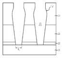
따라서, 도 1에 도시된 바와 같이, 콘택홀 형성시 보잉(100, Bowing)이 발생하고, 콘택 식각시 경사(Slope)에 의해 콘택홀의 바텀CD(200, Bottom Critical Demension)가 작아지게 된다. 이러한 보잉(100)은 콘택홀 간의 거리를 더욱 짧게 만들고, 디자인 룰의 지속적인 감소가 진행되는 경우 콘택홀 사이의 짧은 거리로 인해 콘택홀 간의 브릿지(Bridge)를 유발하는 문제점이 있다.Therefore, as illustrated in FIG. 1, bowing occurs when forming the contact hole, and the bottom
콘택홀 간의 브릿지를 방지하기 위해 콘택홀 형성 후 스페이서를 형성하고 있다.In order to prevent the bridges between the contact holes, spacers are formed after the contact holes are formed.
도 2는 종래 기술에 따른 반도체 소자의 콘택홀 제조방법을 나타내는 공정 단면도이다.2 is a cross-sectional view illustrating a method of manufacturing a contact hole in a semiconductor device according to the related art.
도 2에 도시된 바와 같이, 기판(11) 상에 식각정지용 질화막(12)을 형성하고, 질화막(12) 상에 희생층산화막(13)을 형성한다. 그리고, 희생층산화막(13) 및 질화막(12)을 식각하여 콘택홀(14)을 형성한다. 그리고, 콘택홀(14)을 포함하는 전면에 스페이서용 산화막(15)을 형성한다.As shown in FIG. 2, an etch
위와 같이, 종래 기술은 콘택홀(14)을 형성한 후 스페이서용 산화막(15)을 추가로 형성함으로써 콘택홀(14) 식각시 보잉에 의해 콘택홀(14) 간의 거리가 짧아져 발생하는 브릿지를 방지할 수 있다.As described above, according to the related art, after forming the
그러나, 종래 기술은 스페이서용 산화막(15)에 의해 바텀CD가 더욱 좁아지는 문제점이 있다. 바텀CD가 더욱 좁아지면 후속 공정에서 실린더형 캐패시터를 형성하기 위해 희생층산화막(13) 제거시 캐패시터가 쓰러지는 문제가 발생할 수 있다. 또한, 스페이서용 산화막(15)을 형성한 후 콘택홀(14) 바닥을 오픈시키기 위한 식각공정시 바닥부에 형성된 산화막(15)의 제거가 어려운 문제가 있다.However, the prior art has a problem that the bottom CD is further narrowed by the
본 발명은 상기한 종래 기술의 문제점을 해결하기 위해 제안된 것으로, 캐패시터를 위한 콘택홀 형성시 보잉에 의한 브릿지를 방지할 수 있는 반도체 소자의 제조방법을 제공하는데 그 목적이 있다.The present invention has been proposed to solve the above problems of the prior art, and an object thereof is to provide a method of manufacturing a semiconductor device capable of preventing bridges due to bowing when forming a contact hole for a capacitor.
또한, 콘택홀 바텀CD를 제어할 수 있는 반도체 소자의 제조방법을 제공하는데 그 목적이 있다.Another object of the present invention is to provide a method of manufacturing a semiconductor device capable of controlling a contact hole bottom CD.
상기 목적을 달성하기 위한 본 발명의 반도체 소자의 제조방법은 기판 상에 식각정지막을 형성하는 단계; 상기 식각정지막 상에 제1절연층 및 상기 제1절연층과 식각율이 서로 다른 제2절연층을 적층하는 단계; 상기 식각정지막, 제1절연층 및 제2절연층을 일부 식각하여 콘택홀을 형성하는 단계; 상기 제1절연층 및 식각정지막의 폭을 확장하는 단계; 상기 콘택홀의 표면을 따라 보호막을 형성하는 단계; 상기 콘택홀 바닥의 보호막을 제거하는 단계를 포함하는 것을 특징으로 한다.Method of manufacturing a semiconductor device of the present invention for achieving the above object comprises the steps of forming an etch stop film on a substrate; Stacking a first insulating layer and a second insulating layer having different etching rates from the first insulating layer on the etch stop layer; Forming a contact hole by partially etching the etch stop layer, the first insulating layer, and the second insulating layer; Extending widths of the first insulating layer and the etch stop layer; Forming a protective film along a surface of the contact hole; And removing the protective film on the bottom of the contact hole.
특히, 제1, 제2절연층 및 보호막은 산화막이고, 식각정지막은 질화막이며, 제1절연층의 폭을 확장하는 단계는 습식식각으로 실시하되 제2절연층보다 제1절연층의 식각율이 더 빠른 조건으로 실시할 수 있고, HF 또는 BOE을 사용할 수 있다.In particular, the first and second insulating layers and the passivation layer are oxide films, the etch stop layer is a nitride film, and the step of expanding the width of the first insulating layer is performed by wet etching, but the etching rate of the first insulating layer is higher than that of the second insulating layer. It can be done at faster conditions and HF or BOE can be used.
또한, 식각정지막의 폭을 확장하는 단계는 건식 또는 습식식각으로 실시하되 습식식각은 인산을 사용하는 것을 특징으로 한다.In addition, the step of extending the width of the etch stop layer is performed by dry or wet etching, the wet etching is characterized in that using phosphoric acid.
상술한 본 발명에 의한 반도체 소자의 제조방법은 콘택홀의 바텀CD를 확장할 수 있는 효과가 있다.The method of manufacturing a semiconductor device according to the present invention described above has the effect of extending the bottom CD of the contact hole.
따라서, 콘택홀 식각시 발생하는 보잉을 보완하기 위한 보호막을 형성할 수 있어서 보잉에 의한 콘택홀 간의 브릿지를 방지할 수 있는 효과가 있다.Therefore, a protective film may be formed to compensate for the bowing generated during the contact hole etching, thereby preventing the bridge between the contact holes due to the bowing.
또한, 콘택홀 바닥의 보호막 제거를 용이하게 하는 효과가 있다.In addition, there is an effect to facilitate the removal of the protective film on the bottom of the contact hole.
또한, 하부전극 형성 후 딥아웃 공정에서 하부전극이 쓰러지는 현상을 방지할 수 있는 효과가 있다.In addition, there is an effect that can prevent a phenomenon that the lower electrode collapses in the dipout process after forming the lower electrode.
이하, 본 발명이 속하는 기술 분야에서 통상의 지식을 가진 자가 본 발명의 기술적 사상을 용이하게 실시할 수 있을 정도로 상세히 설명하기 위하여, 본 발명의 가장 바람직한 실시예를 첨부 도면을 참조하여 설명하기로 한다.Hereinafter, the most preferred embodiments of the present invention will be described in detail with reference to the accompanying drawings so that those skilled in the art can easily implement the technical idea of the present invention. .
도 3a 내지 도 3h는 본 발명의 실시예에 따른 반도체 소자의 캐패시터 제조방법을 나타내는 공정 단면도이다.3A to 3H are cross-sectional views illustrating a method of manufacturing a capacitor of a semiconductor device in accordance with an embodiment of the present invention.
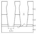
도 3a에 도시된 바와 같이, 기판(21) 상에 식각정지막(22)을 형성한다. 기판(21)은 DRAM공정이 진행되는 반도체(실리콘) 기판일 수 있고, 게이트패턴 및 비트라인패턴 등의 소정공정이 완료된 기판일 수 있다. 식각정지막(22)은 후속공정에서 상부층 식각시 식각선택비를 확보하여 기판(21)이 손실되는 것을 방지하고, 실 린더형 캐패시터를 형성하기 위한 딥아웃 공정에 사용되는 용액이 기판(21)으로 침투하는 것을 방지하기 위한 것이다. 이를 위해, 식각정지막(22)은 상부층과 식각선택비를 갖는 물질로 형성하되, 질화막으로 형성할 수 있다. 또한, 식각정지막(22)을 형성하기 전에 기판(21) 상에 버퍼산화막(도시생략)을 먼저 형성하여 후속 콘택홀 식각시 식각정지막(22)의 식각에 의한 기판(21)의 손실을 방지할 수 있다.As shown in FIG. 3A, an
이어서, 식각정지막(22) 상에 희생막을 형성한다. 이때, 희생막은 식각선택비가 서로 다른 적층막으로 형성될 수 있는데 제1희생막(23) 및 제1희생막(23)과 식각선택비가 다른 제2희생막(24)으로 형성할 수 있다. 이때, 제1 및 제2희생막(23, 24)은 산화막일 수 있고, 특히 제1희생막(23)은 PSG일 수 있고, 제2희생막(24)은 TEOS일 수 있다.Subsequently, a sacrificial layer is formed on the
이어서, 식각정지막(22), 제1 및 제2희생막(23, 24)을 식각하여 기판(21)을 노출시키는 콘택홀(25)을 형성한다. 콘택홀(25)은 제2희생막(24) 상에 감광막을 코팅(Coating)하고 노광 및 현상으로 콘택홀 예정지역이 오픈되도록 패터닝하여 감광막패턴을 형성한 후, 감광막패턴을 식각배리어로 식각정지막(22), 제1 및 제2희생막(23, 24)을 식각하여 형성할 수 있다.Subsequently, the
특히, 콘택홀(25)을 형성하기 위한 식각공정에서 콘택홀(25)의 상부쪽에 보잉('B', Bowing)이 발생할 수 있고, 식각이 진행되면서 경사(Slope)가 발생하여 콘택홀(25)의 바텀CD(W1, Bottom Critical Demension)는 탑CD(Top CD)보다 작게 형성될 수 있다.In particular, in an etching process for forming the
도 3b에 도시된 바와 같이, 제1희생막(23)의 폭을 확장한다. 이를 위해, 습식식각을 실시할 수 있고, 습식식각은 HF 또는 BOE(Buffered Oxide Etchant)를 사용하여 실시할 수 있다.As shown in FIG. 3B, the width of the first
위와 같이, HF 또는 BOE를 사용하여 습식식각을 실시하면 제2희생막(24)보다 식각율이 빠른 제1희생막(23)의 식각이 더 빨리 진행된다. 즉, 제1희생막(23)은 P21에서 P22로 충분한 폭을 확장시킬 수 있고, 제1희생막(23)보다 식각율이 느린 제2희생막(24)의 경우 P11에서 P12로 손실이 발생할 수 있지만 이는 제1희생막(23)의 폭 증가에 비하여 미미한 정도에 불과하며, 콘택홀(25) 간의 간격이 좁아 지는데 큰 영향을 미치지 않는다. 또한, HF 또는 BOE는 산화막을 식각하기 위한 것으로, 식각정지막(22)은 손실되지 않는다.As described above, when the wet etching is performed using the HF or the BOE, the etching of the first
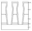
도 3c에 도시된 바와 같이, 식각정지막(22)의 폭을 확장한다. 이를 위해 건식 또는 습식식각을 실시할 수 있고, 건식식각은 플라즈마 식각을 사용할 수 있고, 습식식각은 인산(H3PO4)을 사용하여 실시할 수 있다.As shown in FIG. 3C, the width of the
위와 같이, 건식 또는 습식식각으로 실시함으로써 식각정지막(22)은 P31에서 P32로 폭이 넓어지고, 이때 건식 또는 습식식각이 질화막을 식각하기 위한 조건으로 실시되기 때문에 제1 및 제2희생막(23, 24)은 손실되지 않는다.As described above, by performing dry or wet etching, the
제1희생막(23) 및 식각정지막(22)의 폭을 확장함으로써 콘택홀(25)의 하부의 폭이 넓어지고, 이에 따라 콘택홀(25)의 바텀CD(W2, W2>W1)가 증가하게 된다.The first
도 3d에 도시된 바와 같이, 콘택홀(25)의 표면을 따라 전체구조 상에 보호막(26)을 형성한다. 보호막(26)은 콘택홀(25) 식각시 콘택홀(25)의 상부쪽에 형성된 보잉에 의해 콘택홀(25) 간의 간격이 좁아지는 것을 보완하기 위한 것으로, 제1 및 제2희생층(23, 24)와 동일한 산화막계열일 수 있고, 예컨대 LPTEOS(Low Pressure Tetra Etyle Oxide Silicate) 또는 USG(Un-doped Silicate Glass)일 수 있다.As shown in FIG. 3D, the
위와 같이, 보호막(26)을 형성하면 보잉에 의해 콘택홀(25) 간의 간격이 좁아지는 것을 보완하여 보잉으로 인해 발생하는 콘택홀(25) 간의 브릿지(Bridge)를 방지할 수 있다. 또한, 보호막(26)을 LPTEOS 또는 USG로 형성하는 경우 스텝커버리지가 나빠서 측벽 및 하부에 비해 상부가 더 두껍게 형성된다.As described above, when the
도 3e에 도시된 바와 같이, 콘택홀(25) 바닥의 보호막(26)을 제거한다. 콘택홀(25) 바닥의 보호막(26)을 제거하기 위해 에치백(Etch Back)을 실시할 수 있다. 이때, 에치백은 콘택홀(25) 바닥의 보호막(26)을 제거하기 위해 실시하기 때문에 제2희생막(24) 상부에 형성된 보호막(26)은 모두 제거되지 않을 수 있다. 또한, 에치백의 특성상 모서리 부분의 식각이 더 빨리 진행되어 콘택홀(25)의 어깨부에 형성된 보호막(26)은 거의 손실될 수 있다.As shown in FIG. 3E, the
특히, 도 3b 및 도 3c에서 제1희생막(23) 및 식각정지막(22)의 폭을 선택적으로 넓혀 콘택홀(25)의 바텀CD를 확장함으로써 콘택홀(25) 바닥의 보호막(26) 제거시 바텀CD가 좁아서 제거되지 않는 문제를 방지할 수 있다.In particular, in FIG. 3B and FIG. 3C, the widths of the first
이하, 식각된 보호막(26)을 '보호막패턴(26A)'이라고 한다.Hereinafter, the etched
도 3f에 도시된 바와 같이, 콘택홀(25)의 표면을 따라 하부전극(27)을 형성한다. 하부전극(27)은 콘택홀(25)의 표면을 따라 전체구조 상에 하부전극용 도전층을 형성하고, 도전층을 분리하여 콘택홀(25) 내부에만 잔류하도록 식각함으로써 형성할 수 있다. 이때, 도전층은 금속성막으로 형성할 수 있고, 예컨대 티타늄질화막(TiN)으로 형성할 수 있다. 또한, 도전층을 콘택홀(25) 내부에 잔류시키기 위한 식각은 에치백(Etch Back) 또는 화학적기계적연마(Chemical Mechanical Polishing)공정으로 실시할 수 있다.As shown in FIG. 3F, the
도 3g에 도시된 바와 같이, 딥아웃(Dip Out)을 실시하여 제1 및 제2희생층(23, 24)과 보호막패턴(26A)을 제거한다. 딥아웃은 산화막을 식각하기 위한 용액으로 실시하되 HF 또는 BOE로 실시할 수 있다. 이때, 식각정지막(22)은 딥아웃 용액이 기판(21)으로 들어가는 것을 방지할 수 있다.As shown in FIG. 3G, a dip out is performed to remove the first and second
특히, 딥아웃 공정시 하부전극(27)이 쓰러지는 것을 방지할 수 있는데 이는 도 3b 및 도 3c에서 콘택홀(25)의 바텀CD를 확장함으로써 하부전극(27)의 바닥부가 넓게 형성되었기 때문이다.In particular, it is possible to prevent the
딥아웃 공정에 의해 제1 및 제2희생층(23, 24)과 보호막패턴(26A)이 제거되어 하부전극(27)만 잔류하게 된다. 이때, 하부전극(27)을 실린더형(Cylinder Type)으로 형성된다.The first and second
도 3h에 도시된 바와 같이, 하부전극(27)을 포함하는 전체 구조 상에 유전막(28) 및 상부전극(29)을 적층하여 실린더형 캐패시터를 형성한다. 유전막(28)은 예컨대 금속산화막으로 형성할 수 있고, 상부전극(29)은 하부전극(27)과 동일한 물 질로 형성할 수 있으며 예컨대 티타늄질화막으로 형성할 수 있다.As shown in FIG. 3H, the dielectric film 28 and the
본 발명의 실시예에서는 실린더형 캐패시터를 형성하였으나, 딥아웃 공정으로 제1 및 제2희생층(23, 24)과 보호막패턴(26A)을 제거하지 않고, 하부전극(27)을 포함하는 전체 구조 상에 유전막(28) 및 상부전극(29)을 적층하여 콘케이브형 캐패시터도 형성할 수 있다.In the exemplary embodiment of the present invention, the cylindrical capacitor is formed, but the entire structure including the
또한, 본 발명의 실시예에서는 캐패시터를 형성하기 위한 콘택홀 외에 높은 종횡비를 갖는 콘택홀을 형성하는 반도체 소자에 응용이 가능하다.In addition, the embodiment of the present invention can be applied to a semiconductor device for forming a contact hole having a high aspect ratio in addition to the contact hole for forming a capacitor.
본 발명의 기술 사상은 상기 바람직한 실시예에 따라 구체적으로 기술되었으나, 상기한 실시예는 그 설명을 위한 것이며 그 제한을 위한 것이 아님을 주의하여야 한다. 또한, 본 발명의 기술 분야의 통상의 전문가라면 본 발명의 기술 사상의 범위 내에서 다양한 실시예가 가능함을 이해할 수 있을 것이다.Although the technical idea of the present invention has been described in detail according to the above preferred embodiment, it should be noted that the above-described embodiment is for the purpose of description and not of limitation. In addition, those skilled in the art will understand that various embodiments are possible within the scope of the technical idea of the present invention.
도 1은 종래 기술의 문제점을 나타내는 TEM사진,1 is a TEM photograph showing a problem of the prior art;
도 2는 종래 기술에 따른 반도체 소자의 콘택홀을 나타내는 단면도,2 is a cross-sectional view showing a contact hole of a semiconductor device according to the prior art;
도 3a 내지 도 3h는 본 발명의 실시예에 따른 반도체 소자의 캐패시터 제조방법을 나타내는 공정 단면도.3A to 3H are cross-sectional views illustrating a method of manufacturing a capacitor of a semiconductor device in accordance with an embodiment of the present invention.
* 도면의 주요 부분에 대한 부호의 설명* Explanation of symbols for the main parts of the drawings
21 : 기판22 : 식각정지막21
23 : 제1희생막24 : 제2희생막23: the first sacrificial membrane 24: the second sacrificial membrane
25 : 콘택홀26 : 보호막25
27 : 하부전극28 : 유전막27: lower electrode 28: dielectric film
29 : 상부전극29: upper electrode
Claims (14)
Translated fromKoreanPriority Applications (1)
| Application Number | Priority Date | Filing Date | Title |
|---|---|---|---|
| KR1020070081074AKR20090016813A (en) | 2007-08-13 | 2007-08-13 | Manufacturing method of semiconductor device |
Applications Claiming Priority (1)
| Application Number | Priority Date | Filing Date | Title |
|---|---|---|---|
| KR1020070081074AKR20090016813A (en) | 2007-08-13 | 2007-08-13 | Manufacturing method of semiconductor device |
Publications (1)
| Publication Number | Publication Date |
|---|---|
| KR20090016813Atrue KR20090016813A (en) | 2009-02-18 |
Family
ID=40685723
Family Applications (1)
| Application Number | Title | Priority Date | Filing Date |
|---|---|---|---|
| KR1020070081074AWithdrawnKR20090016813A (en) | 2007-08-13 | 2007-08-13 | Manufacturing method of semiconductor device |
Country Status (1)
| Country | Link |
|---|---|
| KR (1) | KR20090016813A (en) |
Cited By (4)
| Publication number | Priority date | Publication date | Assignee | Title |
|---|---|---|---|---|
| US8252655B2 (en) | 2009-12-14 | 2012-08-28 | Samsung Electronics Co., Ltd. | Method of forming semiconductor cell structure, method of forming semiconductor device including the semiconductor cell structure, and method of forming semiconductor module including the semiconductor device |
| KR20190062028A (en)* | 2017-11-28 | 2019-06-05 | 삼성전자주식회사 | Semiconductor storage device |
| CN111326655A (en)* | 2018-12-13 | 2020-06-23 | 夏泰鑫半导体(青岛)有限公司 | Semiconductor device and method for manufacturing the same |
| US12396148B2 (en) | 2022-03-31 | 2025-08-19 | Samsung Electronics Co., Ltd. | Method of manufacturing integrated circuit device |
- 2007
- 2007-08-13KRKR1020070081074Apatent/KR20090016813A/ennot_activeWithdrawn
Cited By (5)
| Publication number | Priority date | Publication date | Assignee | Title |
|---|---|---|---|---|
| US8252655B2 (en) | 2009-12-14 | 2012-08-28 | Samsung Electronics Co., Ltd. | Method of forming semiconductor cell structure, method of forming semiconductor device including the semiconductor cell structure, and method of forming semiconductor module including the semiconductor device |
| KR20190062028A (en)* | 2017-11-28 | 2019-06-05 | 삼성전자주식회사 | Semiconductor storage device |
| CN111326655A (en)* | 2018-12-13 | 2020-06-23 | 夏泰鑫半导体(青岛)有限公司 | Semiconductor device and method for manufacturing the same |
| CN111326655B (en)* | 2018-12-13 | 2023-10-17 | 夏泰鑫半导体(青岛)有限公司 | Semiconductor device and method for manufacturing the same |
| US12396148B2 (en) | 2022-03-31 | 2025-08-19 | Samsung Electronics Co., Ltd. | Method of manufacturing integrated circuit device |
Similar Documents
| Publication | Publication Date | Title |
|---|---|---|
| JP5105824B2 (en) | Method for forming mask structure and method for forming fine pattern using the same | |
| KR20080088276A (en) | Capacitor Manufacturing Method of Semiconductor Device | |
| KR20120004212A (en) | Capacitor Manufacturing Method | |
| KR20090016813A (en) | Manufacturing method of semiconductor device | |
| TWI466181B (en) | Method of forming a conductive contact of a semiconductor element having a small height difference, a method of forming a semiconductor element | |
| KR101043734B1 (en) | Semiconductor device manufacturing method | |
| KR100948092B1 (en) | Capacitor Manufacturing Method of Semiconductor Device | |
| KR100329072B1 (en) | Capacitor Manufacturing Method for Semiconductor Devices | |
| KR100211542B1 (en) | Capacitor Manufacturing Method of Semiconductor Device | |
| KR100324934B1 (en) | Method of manufacturing semiconductor memory device | |
| KR100886641B1 (en) | Capacitor Manufacturing Method of Semiconductor Device | |
| KR100329743B1 (en) | Method for forming cylinder type bottom electrode | |
| KR100682195B1 (en) | Storage Node Formation Method of Semiconductor Capacitor | |
| KR20010063707A (en) | Method of manufacturing a capacitor in a semiconductor device | |
| KR100745873B1 (en) | Manufacturing Method of Semiconductor Device | |
| KR101161216B1 (en) | method of forming capacitor of MDL device | |
| KR100967679B1 (en) | Method of manufacturing semiconductor device | |
| KR100744002B1 (en) | Manufacturing method of semiconductor device | |
| KR20100076763A (en) | Method for fabricating fine pattern in semiconductor device | |
| KR20080062011A (en) | Manufacturing method of semiconductor device | |
| KR20110076661A (en) | Method of forming fine pattern of semiconductor device | |
| KR20090045715A (en) | Capacitor Manufacturing Method of Semiconductor Device | |
| KR20050116487A (en) | Method for fabrication of semiconductor device | |
| KR20030054271A (en) | Method for forming the gate electrode in semiconductor device | |
| KR19990055768A (en) | Manufacturing method of semiconductor device |
Legal Events
| Date | Code | Title | Description |
|---|---|---|---|
| PA0109 | Patent application | Patent event code:PA01091R01D Comment text:Patent Application Patent event date:20070813 | |
| PG1501 | Laying open of application | ||
| PC1203 | Withdrawal of no request for examination | ||
| WITN | Application deemed withdrawn, e.g. because no request for examination was filed or no examination fee was paid |