KR20090011901A - Method of forming a semiconductor device - Google Patents
Method of forming a semiconductor deviceDownload PDFInfo
- Publication number
- KR20090011901A KR20090011901AKR1020070075940AKR20070075940AKR20090011901AKR 20090011901 AKR20090011901 AKR 20090011901AKR 1020070075940 AKR1020070075940 AKR 1020070075940AKR 20070075940 AKR20070075940 AKR 20070075940AKR 20090011901 AKR20090011901 AKR 20090011901A
- Authority
- KR
- South Korea
- Prior art keywords
- pattern
- target layer
- bar
- forming
- patterns
- Prior art date
- Legal status (The legal status is an assumption and is not a legal conclusion. Google has not performed a legal analysis and makes no representation as to the accuracy of the status listed.)
- Withdrawn
Links
Images


Classifications
- G—PHYSICS
- G03—PHOTOGRAPHY; CINEMATOGRAPHY; ANALOGOUS TECHNIQUES USING WAVES OTHER THAN OPTICAL WAVES; ELECTROGRAPHY; HOLOGRAPHY
- G03F—PHOTOMECHANICAL PRODUCTION OF TEXTURED OR PATTERNED SURFACES, e.g. FOR PRINTING, FOR PROCESSING OF SEMICONDUCTOR DEVICES; MATERIALS THEREFOR; ORIGINALS THEREFOR; APPARATUS SPECIALLY ADAPTED THEREFOR
- G03F7/00—Photomechanical, e.g. photolithographic, production of textured or patterned surfaces, e.g. printing surfaces; Materials therefor, e.g. comprising photoresists; Apparatus specially adapted therefor
- G03F7/70—Microphotolithographic exposure; Apparatus therefor
- G03F7/70425—Imaging strategies, e.g. for increasing throughput or resolution, printing product fields larger than the image field or compensating lithography- or non-lithography errors, e.g. proximity correction, mix-and-match, stitching or double patterning
- G03F7/70466—Multiple exposures, e.g. combination of fine and coarse exposures, double patterning or multiple exposures for printing a single feature
- H—ELECTRICITY
- H01—ELECTRIC ELEMENTS
- H01L—SEMICONDUCTOR DEVICES NOT COVERED BY CLASS H10
- H01L21/00—Processes or apparatus adapted for the manufacture or treatment of semiconductor or solid state devices or of parts thereof
- H01L21/02—Manufacture or treatment of semiconductor devices or of parts thereof
- H01L21/027—Making masks on semiconductor bodies for further photolithographic processing not provided for in group H01L21/18 or H01L21/34
- H01L21/033—Making masks on semiconductor bodies for further photolithographic processing not provided for in group H01L21/18 or H01L21/34 comprising inorganic layers
- H01L21/0334—Making masks on semiconductor bodies for further photolithographic processing not provided for in group H01L21/18 or H01L21/34 comprising inorganic layers characterised by their size, orientation, disposition, behaviour, shape, in horizontal or vertical plane
- H01L21/0337—Making masks on semiconductor bodies for further photolithographic processing not provided for in group H01L21/18 or H01L21/34 comprising inorganic layers characterised by their size, orientation, disposition, behaviour, shape, in horizontal or vertical plane characterised by the process involved to create the mask, e.g. lift-off masks, sidewalls, or to modify the mask, e.g. pre-treatment, post-treatment
- H—ELECTRICITY
- H01—ELECTRIC ELEMENTS
- H01L—SEMICONDUCTOR DEVICES NOT COVERED BY CLASS H10
- H01L21/00—Processes or apparatus adapted for the manufacture or treatment of semiconductor or solid state devices or of parts thereof
- H01L21/02—Manufacture or treatment of semiconductor devices or of parts thereof
- H01L21/027—Making masks on semiconductor bodies for further photolithographic processing not provided for in group H01L21/18 or H01L21/34
- H01L21/033—Making masks on semiconductor bodies for further photolithographic processing not provided for in group H01L21/18 or H01L21/34 comprising inorganic layers
- H01L21/0334—Making masks on semiconductor bodies for further photolithographic processing not provided for in group H01L21/18 or H01L21/34 comprising inorganic layers characterised by their size, orientation, disposition, behaviour, shape, in horizontal or vertical plane
- H01L21/0338—Process specially adapted to improve the resolution of the mask
Landscapes
- Engineering & Computer Science (AREA)
- Physics & Mathematics (AREA)
- General Physics & Mathematics (AREA)
- Chemical & Material Sciences (AREA)
- Inorganic Chemistry (AREA)
- Condensed Matter Physics & Semiconductors (AREA)
- Manufacturing & Machinery (AREA)
- Computer Hardware Design (AREA)
- Microelectronics & Electronic Packaging (AREA)
- Power Engineering (AREA)
- Internal Circuitry In Semiconductor Integrated Circuit Devices (AREA)
- Drying Of Semiconductors (AREA)
Abstract
Translated fromKoreanDescription
Translated fromKorean본 발명은 반도체 소자의 미세 패턴 형성 방법에 관한 것으로, 보다 상세하게는 이중 패터닝 기술을 이용한 반도체 소자의 미세 패턴 형성 방법에 관한 것이다.The present invention relates to a method of forming a fine pattern of a semiconductor device, and more particularly, to a method of forming a fine pattern of a semiconductor device using a double patterning technique.
반도체 소자를 고집적화하기 위해서는 패턴의 미세화가 필수적이다. 좁은 면적에 많은 소자를 집적시키기 위하여 개별 단위 소자의 크기를 작게 형성하여야 하며, 이를 위하여 형성하고자 하는 패턴의 폭과 간격의 합인 피치(P, pitch)를 작게 하여야 한다. 최근, 소자 디자인 룰(design rule)의 감소가 급격히 진행됨에 따라 반도체 소자 구현에 필요한 패턴, 특히 라인 앤드 스페이스 패턴(line and space pattern)을 형성하기 위한 포토리소그래피 공정에 있어서 해상 한계로 인하여 미세 피치를 가지는 패턴을 형성하는 데 한계가 있다.In order to highly integrate a semiconductor device, pattern refinement is essential. In order to integrate a large number of devices in a small area, the size of the individual unit devices should be made small. For this purpose, the pitch (P, pitch), which is the sum of the width and the interval of the pattern to be formed, should be made small. Recently, as the reduction of device design rules has progressed rapidly, fine pitch has been reduced due to the resolution limitation in the photolithography process for forming a pattern, particularly a line and space pattern, required for semiconductor device implementation. Branches are limited in forming patterns.
상술한 포토리소그래피 공정에서의 해상 한계를 극복하기 위하여 이중 패터닝 기술을 이용한 미세 패턴 형성 방법이 제안되었다.In order to overcome the resolution limitation in the photolithography process described above, a method of forming a fine pattern using a double patterning technique has been proposed.
도 1a 내지 도 1j는 종래 기술에 의해 반도체 소자를 형성하는 제1 방법을 도해한 단면도들이다.1A to 1J are cross-sectional views illustrating a first method of forming a semiconductor device by the prior art.
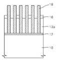
도 1a을 참조하면, ILD를 형성하는 대상막(10) 상에 식각저지층(12), 산화막(13), 폴리실리콘막(14)을 차례로 적층한 후 제1 감광막 패턴(15)을 형성한다. 도 1b를 참조하면, 제1 감광막 패턴(15)을 식각마스크로 하여 제1 폴리실리콘막(14)을 식각하여 제1 폴리실리콘막 패턴(14a)을 형성한다. 도 1c을 참조하면, 제1 폴리실리콘막 패턴(14a) 상에 스페이서 산화막(16)을 증착한다. 도 1d 내지 도 1e를 참조하면, 스페이서 산화막(16) 상에 제2 폴리실리콘막 패턴(17)을 형성한다. 제2 폴리실리콘막 패턴(17)은 폴리실리콘막을 스페이서 산화막(16) 상에 증착한 후 에치백 또는 화학기계적 연마 공정을 적용하여 형성할 수 있다. 제1 폴리실리콘막 패턴(14a) 및 제2 폴리실리콘막 패턴(17)을 식각마스크로 하여 스페이서 산화막(16)을 식각한 후 계속하여 산화막(13)을 식각하여 제1 산화막 패턴(13a)을 형성한다. 도 1f 내지 도 1h을 참조하면, 이후에 SOH 패턴(18)을 제1 산화막 패턴(13a) 주위에 형성시킨다. 계속하여 SOH 패턴(18)을 식각마스크로 하여 제1 폴리실리콘막 패턴(14a) 및 제2 폴리실리콘막 패턴(17)을 식각하여 제거한다. 계속하여 SOH 패턴(18)을 식각마스크로 하여 제1 산화막 패턴(13a)을 식각하여 제거하면 대상막(10) 상에 SOH 패턴(18)이 식각 마스크로 형성된 구조가 완성된다. 도 1i 내지 도 1j를 참조하면, SOH 패턴(18)을 식각마스크로 하여 대상막(10)을 식각하여 대상막 패턴(10a)이 완성된다.Referring to FIG. 1A, an
도 2a 내지 도 2h은 종래 기술에 의해 반도체 소자를 형성하는 제2 방법을 도해한 도면들이다.2A to 2H illustrate a second method of forming a semiconductor device according to the prior art.
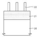
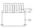
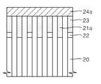
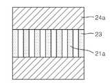
도 2a 내지 도 2b를 참조하면, ILD 의 역할을 담당하는 대상막(20) 상에 제1 폴리실리콘막(21)과 제1 감광막 패턴(22)을 순차적으로 형성한다. 제1 감광막 패턴(22)을 식각마스크로 하여 제1 폴리실리콘막(21)을 식각하여 제1 폴리실리콘막 패턴(21a)을 형성한다. 도 2c 내지 도 2d를 참조하면, 제1 폴리실리콘막 패턴(21a) 상에 스페이서 산화막(22)을 형성하고 계속하여 스페이서 산화막(22) 상에 제2 폴리실리콘막 패턴(23)을 형성한다. 도 2e를 참조하면, 제2 폴리실리콘막 패턴(23)에 직교한 방향으로 ACL막 패턴(24)을 형성한다. 도 2e에 도시된 구조에 대한 평면도인 도 2f을 참조하면, ACL막 패턴(24)은 소정의 간격으로 이격되어 형성된다. 제1 폴리실리콘막 패턴(21a)은 실제로 위에서 보이지는 않지만 편의상 도면에 도시하였다. 도 2g 내지 도 2h을 참조하면, ACL막 패턴(24) 및 제1 폴리실리콘막 패턴(21a)과 제2 폴리실리콘막 패턴(23)을 식각마스크로 하여 스페이서 산화막(22) 및 대상막(20)을 식각하여 콘택 패턴을 형성한다.2A to 2B, the
상기 제1 방법은 포토 공정 수가 적고 SOH 마스크 사용에 의하여 마스크 두께를 증가하여 보우잉(bowing) 현상을 개선할 수 있는 장점이 있지만 형성 방법이 너무 복잡하여 패턴 형성이 어렵고 식각 특성 상 ILD 상부 임계치수를 확보하기 어려운 단점이 있다. 상기 제2 방법은 ILD 상부 임계치수 확보에는 유리하나 마스크 층이 폴리실리콘/ACL 구조로 되어 있어 보우잉에는 취약하다. 이것은 폴리실리콘 마스크인 부분의 두께가 낮아 이온 에너지에 의하여 보우잉 현상이 심하게 발생되는 부위가 폴리실리콘 마스크 아래 부분에 위치하기 때문이다.The first method has the advantage of improving the bowing phenomenon by increasing the mask thickness by using a small number of photo-processes and using an SOH mask, but the formation method is too complicated to form a pattern and the upper critical dimension of the ILD due to etching characteristics. There is a disadvantage that is difficult to secure. The second method is advantageous for securing the ILD upper critical dimension but is vulnerable to bowing since the mask layer has a polysilicon / ACL structure. This is because a portion of the polysilicon mask having a low thickness has a low bowing phenomenon due to ion energy, which is located under the polysilicon mask.
본 발명은, 이를 개선하기 위하여 최종 ILD 식각 마스크로 ACL 등의 하드 마스크를 간단하게 사용할 수 있는 방법을 제공하고자 한다.The present invention is to provide a method that can simply use a hard mask, such as ACL as the final ILD etching mask to improve this.
본 발명이 이루고자 하는 기술적 과제는 공정의 부담을 줄이면서 이중 패터닝 기술을 구현하는 반도체 소자의 제조방법을 제공하는 데 있다.An object of the present invention is to provide a method for manufacturing a semiconductor device that implements a double patterning technology while reducing the burden on the process.
상술한 기술적 과제를 달성하기 위하여, 본 발명의 일 측면에 의한 반도체 소자의 제조방법은 제1 대상막 상에 제2 대상막을 형성하는 단계; 상기 제2 대상막 상에 상기 제2 대상막의 일부를 노출시키는 제3 대상막 패턴을 형성하는 단계; 상기 노출된 제2 대상막 상에 제1 피치의 간격으로 이격된 복수개의 제1 바(bar)형 패턴 및 상기 제3 대상막 패턴 상에 상기 복수개의 제1 바형 패턴과 엇갈리게 배열되고 상기 제1 바형 패턴의 상하의 위치에 각각 상기 제1 피치의 간격으로 이격된 복수개의 제2 바형 패턴을 형성하는 단계; 인접하는 상기 제1 바형 패턴들 사이에 상기 제2 대상막이 노출되는 제1 스페이스 패턴을 형성하도록 상기 복수개의 제1 바형 패턴과 상기 복수개의 제2 바형 패턴의 측면에 폴리머 패턴을 형성하는 단계; 상기 폴리머 패턴 및 상기 제3 대상막 패턴을 식각 마스크로 하여 상기 제1 바형 패턴, 상기 제2 대상막 및 상기 제1 대상막을 식각하는 단계;를 포함한다. 상기 폴리머 패턴을 형성하는 단계는 복수개의 상기 제1 스페이스 패턴이 상기 제1 피치의 간격으로 이격되도록 형성하는 단계를 포함할 수 있다. 인접하는 상기 제1 바형 패턴과 상기 제2 바형 패턴은 마름모꼴을 형성할 수 있다. 상기 제1 스페이스 패턴은 상기 제1 바형 패턴과 함께 일렬로 나란하게 배열될 수 있으며, 상기 제1 바형 패 턴과 크기가 동일한 것이 바람직하다. 상기 제1 대상막은 ACL을 포함하여 구성되고, 상기 제2 대상막은 SiO2를 포함하여 구성되고, 상기 제3 대상막 패턴은 SiON을 포함하여 구성되며, 상기 제1 바형 패턴 및 상기 제2 바형 패턴은 SiO2를 포함하여 구성될 수 있다.In order to achieve the above technical problem, a method of manufacturing a semiconductor device according to an aspect of the present invention comprises the steps of forming a second target film on the first target film; Forming a third target layer pattern on the second target layer to expose a portion of the second target layer; A plurality of first bar-shaped patterns spaced apart at intervals of a first pitch on the exposed second target layer and the plurality of first bar-shaped patterns on the third target layer pattern, and alternately arranged; Forming a plurality of second bar patterns spaced apart at intervals of the first pitch at upper and lower positions of the bar pattern; Forming a polymer pattern on side surfaces of the plurality of first bar patterns and the plurality of second bar patterns so as to form a first space pattern between the adjacent first bar patterns; And etching the first bar pattern, the second target layer, and the first target layer by using the polymer pattern and the third target layer pattern as an etching mask. The forming of the polymer pattern may include forming a plurality of the first space patterns to be spaced apart at intervals of the first pitch. Adjacent the first bar pattern and the second bar pattern may form a rhombus. The first space pattern may be arranged side by side with the first bar pattern, and preferably the same size as the first bar pattern. The first target layer includes an ACL, the second target layer includes SiO2 , the third target layer pattern includes SiON, and the first bar pattern and the second bar pattern. May comprise SiO2 .
상술한 기술적 과제를 달성하기 위하여, 본 발명의 다른 측면에 의한 반도체 소자의 제조방법은 제1 대상막 상에 제2 대상막을 형성하는 단계; 상기 제2 대상막 상에 상기 제2 대상막의 일부를 노출시키는 제3 대상막 패턴을 형성하는 단계; 상기 노출된 제2 대상막 및 인접한 상기 제3 대상막 패턴 상에 제1 피치의 간격으로 이격된 복수개의 제1 바(bar)형 패턴을 형성하는 단계; 인접하는 상기 제1 바형 패턴들 사이에 상기 제2 대상막이 노출되는 제1 스페이스(space) 패턴을 형성하도록 상기 제3 대상막 패턴 및 상기 제2 대상막 상에 상기 제1 바형 패턴의 측면으로 스페이서(spacer) 패턴을 형성하는 단계; 상기 스페이서 패턴 및 상기 제3 대상막 패턴을 식각 마스크로 하여 상기 제1 바형 패턴, 상기 제2 대상막 및 상기 제1 대상막을 식각하는 단계;를 포함한다. 상기 스페이서 패턴을 형성하는 단계는 복수개의 상기 제1 스페이스 패턴이 상기 제1 피치의 간격으로 이격되도록 형성하는 단계를 포함할 수 있다. 상기 스페이서 패턴을 형성하는 단계는 상기 제1 스페이스 패턴의 크기가 제1 바형 패턴이 상기 제2 대상막의 바로 위에 위치하는 부분의 크기와 동일하도록 형성하는 단계를 포함할 수 있다. 상기 제1 스페이스 패턴은 상기 제1 바형 패턴과 함께 일렬로 나란하게 배열되는 것이 바람직하다. 상기 제1 대상막 및 상기 제1 바형 패턴은 ACL을 포함하여 구성되고, 상기 제2 대상막은 SiO2를 포함하여 구성되고, 상기 제3 대상막 패턴은 SiON을 포함하여 구성되며, 상기 스페이서 패턴은 SiO2를 포함하여 구성될 수 있다.In order to achieve the above technical problem, a method of manufacturing a semiconductor device according to another aspect of the present invention comprises the steps of forming a second target film on the first target film; Forming a third target layer pattern on the second target layer to expose a portion of the second target layer; Forming a plurality of first bar patterns spaced apart at intervals of a first pitch on the exposed second target layer and the adjacent third target layer pattern; Spacers on the third target layer pattern and the second target layer to side surfaces of the first bar pattern to form a first space pattern between the adjacent first bar patterns. forming a spacer pattern; And etching the first bar pattern, the second target layer, and the first target layer using the spacer pattern and the third target layer pattern as an etching mask. The forming of the spacer pattern may include forming a plurality of the first space patterns to be spaced apart at intervals of the first pitch. The forming of the spacer pattern may include forming a size of the first space pattern to be equal to a size of a portion of the first bar pattern positioned directly on the second target layer. The first space pattern may be arranged in parallel with the first bar pattern. The first target layer and the first bar pattern may include an ACL, the second target layer may include SiO2 , the third target layer pattern may include SiON, and the spacer pattern may include: SiO2 may be included.
본 발명에 의한 반도체 소자의 제조방법에 따르면, 단순한 공정을 사용하여 임계 치수 조절을 용이하게 하는 이중 패터닝 방법을 사용하여 미세한 패턴을 가지는 반도체 소자를 제조할 수 있다.According to the method for manufacturing a semiconductor device according to the present invention, it is possible to manufacture a semiconductor device having a fine pattern by using a double patterning method that facilitates critical dimension adjustment using a simple process.
이하, 첨부된 도면을 참조하여 본 발명의 바람직한 실시예를 상세히 설명하기로 한다. 그러나, 본 발명은 여기서 설명되어지는 실시예들에 한정되지 않고 다른 형태로 구체화될 수도 있다. 오히려, 여기서 소개되는 실시예들은 개시된 내용이 철저하고 완전해질 수 있도록 그리고 당업자에게 본 발명의 사상이 충분히 전달될 수 있도록 하기 위해 제공되어지는 것이다. 도면들에 있어서, 층 및 영역들의 두께는 명확성을 기하여 위하여 과장되어진 것이다. 명세서 전체에 걸쳐서 막, 영역, 또는 기판등과 같은 하나의 구성요소가 또 다른 구성요소 "상에" 위치한다고 언급할 때는, 상기 하나의 구성요소가 다른 구성요소에 직접 접촉하거나 중간에 개재되는 구성요소들이 존재할 수 있다고 해석될 수 있다.Hereinafter, exemplary embodiments of the present invention will be described in detail with reference to the accompanying drawings. However, the present invention is not limited to the embodiments described herein and may be embodied in other forms. Rather, the embodiments introduced herein are provided to ensure that the disclosed subject matter is thorough and complete, and that the scope of the invention to those skilled in the art will fully convey. In the drawings, the thicknesses of layers and regions are exaggerated for clarity. Throughout the specification, when referring to one component, such as a film, region, or substrate, being "on" another component, the component is in direct contact with or intervening with another component. It can be interpreted that elements may exist.
도 3a 내지 도 3p는 본 발명의 일실시예에 따른 반도체 소자의 형성 방법을 도해하는 도면들이다.3A to 3P illustrate a method of forming a semiconductor device in accordance with an embodiment of the present invention.
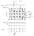
반도체 소자의 단면도인 도 3a과 평면도인 도 3b를 함께 참조하면, ILD 막(31) 상에 제1 대상막(32), 제2 대상막(33) 및 제3 대상막(34)을 순차적으로 형성한 후 제1 감광막 패턴(39)을 형성한다. 본 발명의 일실시예에서는 제1 대상막(32)은 ACL을 포함하여 구성되고, 제2 대상막(33)은 SiO2를 포함하여 구성되고, 제3 대상막 패턴(34)은 SiON을 포함하여 구성되는 것이 바람직하지만 여기에 한정되는 것은 아니다. 이하에서는 상기 구성을 근거로 하여 설명한다. 제1 감광막 패턴은 제3 대상막(34)을 제1폭(W1)만큼 노출시키도록 형성한다. 도 3b에서 게이트 라인(30b)과 액티브 라인(30a)은 점선으로 표시하였는데 액티브 라인(30a)은 제1 대상막(32) 아래에 위치한다.Referring to FIG. 3A, which is a cross-sectional view of the semiconductor device, and FIG. 3B, which is a plan view, the
계속하여 반도체 소자의 단면도인 도 3c와 평면도인 도 3d를 함께 참조하면, 상기 제1 감광막 패턴(39)을 식각마스크로 하여 제3 대상막(34)을 식각하여 제3 대상막 패턴(34a)을 형성한다. 그리고 제3 대상막 패턴(34a) 상에 제4 대상막(35)을 형성한다. 제4 대상막(35)은 제2 대상막(33)과 같은 물질로 구성되며, 바람직하게는 SiO2를 포함하여 구성될 수 있다.Subsequently, referring to FIG. 3C, which is a cross-sectional view of the semiconductor device, and FIG. 3D, which is a plan view, the
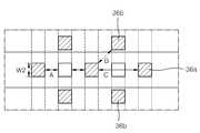
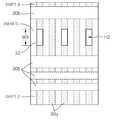
계속하여 반도체 소자의 단면도인 도 3e와 평면도인 도 3f를 함께 참조하면, 제4 대상막(35) 상에 복수개의 제2 감광막 패턴(36a) 및 제3 감광막 패턴(36b)을 형성한다. 복수개의 제2 감광막 패턴(36a) 상기 제1폭(W1)을 가지는 제2 대상막(33) 상에 제1 피치의 간격으로 이격되어 형성된다. 바람직하게는 제2 감광막 패턴(36a)은 상기 제1폭(W1)보다 작은 제2폭(W2)을 가진다. 복수개의 제3 감광막 패 턴(36b)은 제3 대상막 패턴(34a) 상에 형성되는데, 제2 감광막 패턴(36a)과 엇갈리게 배열되고 제2 감광막 패턴(36a)의 상하의 위치에 각각 상기 제1 피치의 간격으로 이격되어 형성된다. 인접하는 제2 감광막 패턴(36a)과 제3 감광막 패턴(36b)은 마름모꼴을 형성하는 것이 바람직하다. 한편, 도 3e에서 제2 감광막 패턴(36a)과 제3 감광막 패턴(36b)은 같은 단면상에서 존재할 수 없지만 편의상 같이 도시하였으며, 이하의 단면도에서 마찬가지로 적용된다.Subsequently, referring to FIG. 3E, which is a cross-sectional view of the semiconductor device, and FIG. 3F, which is a plan view, a plurality of second
도 3g는 도 3f의 일부를 확대하여 도시한 평면도이다.FIG. 3G is an enlarged plan view of a portion of FIG. 3F.
도 3g를 참조하면, 액티브 라인 상에 각각 콘택을 형성하도록 복수개의 제2 감광막 패턴(36a)은 제1간격(A)만큼 공간을 두고 형성되어야 한다. 하지만, 본 발명의 일실시예에 따르면 제2 감광막 패턴(36a)은 제3 감광막 패턴(36b)과 제2간격(B)만큼 공간을 두고 형성되며, 제2 감광막 패턴(36a)들과는 제3간격(C)만큼 공간을 두고 형성될 수 있다. 즉, 제2간격(B)과 제3간격(C)은 제1간격(A)보다 크므로, 포토 및 식각 공정에서 마진을 확보할 수 있다.Referring to FIG. 3G, the plurality of second
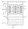
계속하여 반도체 소자의 단면도인 도 3h와 평면도인 도 3i를 함께 참조하면, 제2 감광막 패턴(36a)과 제3 감광막 패턴(36b)을 식각마스크로 하여 제4 대상막(35)을 식각하여 각각 제1 바형 패턴(35a) 및 제2 바형 패턴(35b)을 형성한다. 즉, 노출된 제2 대상막(33) 상에 제1 피치의 간격으로 이격된 복수개의 제1 바(bar)형 패턴(35a)을 형성하고, 제3 대상막 패턴(34a) 상에 복수개의 제1 바형 패턴(35a)과 엇갈리게 배열되고 제1 바형 패턴(35a)의 상하의 위치에 상기 제1 피치의 간격으로 이격된 복수개의 제2 바형 패턴(35b)을 형성한다. 바람직하게는 인 접하는 제1 바형 패턴(35a)과 제2 바형 패턴(35b)은 마름모꼴을 형성할 수 있으며, SiO2를 포함하여 구성될 수 있다. 바람직한 실시예에서는 위치 d는 SiO2/SiON/SiO2/ACL/ILD인 하부 구조를 형성하며, 위치 e는 SiON/SiO2/ACL/ILD인 하부 구조를 형성할 수 있다. 또한 위치 f는 SiO2/ACL/ILD인 하부 구조를 형성하며, 위치 g는 SiO2/ACL/ILD인 하부 구조를 형성할 수 있다.Subsequently, referring to FIG. 3H, which is a cross-sectional view of the semiconductor device, and FIG. 3I, which is a plan view, the
계속하여 반도체 소자의 단면도인 도 3j와 평면도인 도 3k를 함께 참조하면, 인접하는 제1 바형 패턴(35a)들 사이에 제2 대상막(33)이 노출되는 제1 스페이스 패턴을 형성하도록 복수개의 제1 바형 패턴(35a)과 복수개의 제2 바형 패턴(35b)의 측면에 폴리머 패턴(37)을 형성한다. 위치 g에 도시된 상기 제1 스페이스 패턴은 위치 f에 도시된 제1 바형 패턴(35a) 사이에서 형성된다. 폴리머 패턴(37)은 CCP 타입, RIE 타입 또는 ICP 타입의 플라즈마 발생기에서 CH2, CH4 가스와 CH3F 가스 특히 CxHy 또는 CxHyFz 계의 가스와 Ar, He, Ne과 같은 불활성 가스를 혼합하여 형성한다. 폴리머 패턴(37)은 상기 제1 스페이스 패턴이 상기 제1 피치의 간격으로 이격되도록 형성하는 것이 바람직하다. 상기 제1 스페이스 패턴은 제1 바형 패턴(35a)과 함께 일렬로 나란하게 배열되고, 제1 바형 배턴(35a)과 크기가 동일한 것이 바람직하다. 바람직한 실시예에서는 위치 d는 SiO2/SiON/SiO2/ACL/ILD인 하부 구조를 형성하며, 위치 e는 SiON/SiO2/ACL/ILD인 하부 구조를 형성할 수 있다. 또한 위치 f는 SiO2/ACL/ILD인 하부 구조를 형성하며, 위치 g는 SiO2/ACL/ILD인 하부 구조를 형성할 수 있다.Subsequently, referring to FIG. 3J, which is a cross-sectional view of the semiconductor device, and FIG. 3K, which is a plan view, a plurality of first space patterns may be formed between the adjacent first
계속하여 반도체 소자의 단면도인 도 3l과 평면도인 도 3m을 함께 참조하면, 폴리머 패턴(36a) 및 제3 대상막 패턴(34a)을 식각 마스크로 하여 제1 바형 패턴(35a), 제2 바형 패턴(35b)을 식각한다. 바람직한 실시예에서는 위치 d는 SiON/SiO2/ACL/ILD인 하부 구조를 형성하며, 위치 e는 SiON/SiO2/ACL/ILD인 하부 구조를 형성할 수 있다. 또한 위치 f는 ACL/ILD인 하부 구조를 형성하며, 위치 g는 ACL/ILD인 하부 구조를 형성할 수 있다.Subsequently, referring to FIG. 3L, which is a cross-sectional view of the semiconductor device, and FIG. 3M, which is a plan view, the
계속하여 반도체 소자의 단면도인 도 3n과 도 3o를 참조하면, 폴리머 패턴(36a) 또는 제3 대상막 패턴(34a)을 식각 마스크로 하여 제1 대상막(32)을 식각하여 제1 대상막 패턴(32a)을 형성한다. 계속하여 ILD막(31)을 식각하여 제2폭(W2)을 가지는 콘택홀(H1)을 형성한다. 즉, 도 3p를 참조하면, 액티브 라인(30a) 상에 콘택홀(H1)이 형성된 구조를 얻을 수 있다.3N and 3O, which are cross-sectional views of semiconductor devices, the
도 4a 내지 도 4n은 본 발명의 다른 실시예에 따른 반도체 소자의 형성 방법을 도해하는 도면들이다.4A through 4N are diagrams illustrating a method of forming a semiconductor device in accordance with another embodiment of the present invention.
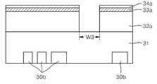
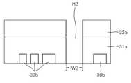
반도체 소자의 단면도인 도 4a과 평면도인 도 4b를 함께 참조하면, ILD 막(31) 상에 제1 대상막(32), 제2 대상막(33)을 형성하고 제3폭(W3)을 가지는 제3 대상막 패턴(34a)을 형성한다. 본 발명의 실시예에서는 제1 대상막(32)은 ACL을 포함하여 구성되고, 제2 대상막(33)은 SiO2를 포함하여 구성되고, 제3 대상막 패턴(34a)은 SiON을 포함하여 구성되는 것이 바람직하지만 여기에 한정되는 것은 아니다. 이하에서는 상기 구성을 근거로 하여 설명한다. 도 4b에서 게이트 라인(30b) 과 액티브 라인(30a)은 점선으로 표시하였는데 액티브 라인(30a)은 제1 대상막(32) 아래에 위치한다.Referring to FIG. 4A, which is a cross-sectional view of a semiconductor device, and FIG. 4B, which is a plan view, a
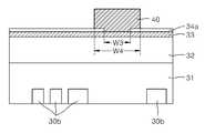
계속하여 반도체 소자의 단면도인 도 4c와 평면도인 도 4d를 함께 참조하면, 제3폭(W3)만큼 노출된 제2 대상막(33) 및 인접한 제3 대상막 패턴(34a) 상에 제1 피치의 간격으로 이격된 복수개의 제1 바(bar)형 패턴(40)을 형성한다. 제1 바형 패턴(40)은 상기 제3폭(W3)보다 큰 제4폭(W4)을 가질 수 있다.Subsequently, referring to FIG. 4C, which is a cross-sectional view of the semiconductor device, and FIG. 4D, which is a plan view, a first pitch is formed on the
계속하여 반도체 소자의 단면도인 도 4e와 평면도인 도 4f를 함께 참조하면,Subsequently, referring to FIG. 4E, which is a cross-sectional view of a semiconductor device, and FIG. 4F, which is a plan view,
인접하는 제1 바형 패턴(40)들 사이에 제2 대상막(33)이 노출되는 제1 스페이스(space) 패턴을 형성하도록 제3 대상막 패턴(34a) 및 제2 대상막(33) 상에 제1 바형 패턴(40)의 측면으로 스페이서(spacer) 패턴(41)을 형성한다. 바람직하게는 스페이서(spacer) 패턴(41)은 SiO2를 포함하여 구성되며, ALD 공정에 의해 형성될 수 있다. 도 4f에서 상기 제1 스페이스 패턴은 스페이서 패턴(41) 사이에 제3폭(W3)을 가지는 위치에 형성된다. 복수개의 상기 제1 스페이스 패턴은 상기 제1 피치의 간격으로 이격되도록 형성될 수 있고, 상기 제1 스페이스 패턴의 크기는 제1 바형 패턴(40)이 제2 대상막(33)의 바로 위에 위치하는 부분의 크기와 동일한 것이 바람직하다. 한편, 상기 제1 스페이스 패턴은 제1 바형 패턴(40)과 함께 일렬로 나란하게 배열되는 것이 바람직하다.On the third
계속하여 반도체 소자의 단면도인 도 4g와 평면도인 도 4h를 함께 참조하면, 스페이서 패턴(41) 및 제3 대상막 패턴(34a)을 식각 마스크로 하여 제1 바형 패턴(40)을 식각하여 제거한다. 상기 식각 공정은 애싱 공정을 포함한다.Subsequently, referring to FIG. 4G, which is a sectional view of the semiconductor device, and FIG. 4H, which is a plan view, the
계속하여 반도체 소자의 단면도인 도 4i와 평면도인 도 4j를 함께 참조하면, 스페이서 패턴(41a) 및 제3 대상막 패턴(34a)을 식각 마스크로 하여 노출된 제2 대상막(33)을 식각하여 제1 대상막(32)이 노출되도록 한다. 상기 식각되는 제2 대상막(33)은 제1 바형 패턴(40)의 아래에 있는 제2 대상막과 상기 제1 스페이스 패턴에 노출된 제2 대상막으로 구성된다.Subsequently, referring to FIG. 4I, which is a cross-sectional view of the semiconductor device, and FIG. 4J, which is a plan view, the exposed
계속하여 반도체 소자의 단면도인 도 4k와 평면도인 도 4l을 함께 참조하면, 스페이서 패턴(41a) 및 제3 대상막 패턴(34a)을 식각 마스크로 하여 노출된 제1 대상막(32)을 식각하여 제1 대상막 패턴(32a)를 형성하고 ILD막(31)이 노출되도록 한다.Subsequently, referring to FIG. 4K, which is a cross-sectional view of the semiconductor device, and FIG. 4L, which is a plan view, the exposed
계속하여 반도체 소자의 단면도인 도 4m과 평면도인 도 4n을 함께 참조하면, 스페이서 패턴(41a), 제3 대상막 패턴(34a) 또는 제1 대상막 패턴(32b)을 식각 마스크로 하여 노출된 ILD막(1)을 식각하여 콘택홀(H2)을 형성한다. 즉, 액티브 라인(30a) 상에 콘택홀(H2)이 형성된 구조를 얻을 수 있다.Subsequently, referring to FIG. 4M, which is a cross-sectional view of the semiconductor device, and FIG. 4N, which is a plan view, an ILD exposed using the
일반적으로 ACL 증착 온도보다 SiO2의 증착 온도 및 SiON의 증착 온도가 낮으므로 ACL 마스크 위에서 이중 패터닝을 할 수 있게 되었다. 따라서 ACL 마스크를 사용할 수 있게 되어 임계 치수 조절이 용이한 이중 패터닝 공정을 확보할 수 있게 되었다.In general, the deposition temperature of SiO 2 and the deposition temperature of SiON are lower than the ACL deposition temperature, thereby enabling double patterning on the ACL mask. As a result, the use of an ACL mask allows for a double patterning process that is easy to adjust critical dimensions.
발명의 특정 실시예들에 대한 이상의 설명은 예시 및 설명을 목적으로 제공되었다. 따라서, 본 발명은 상기 실시예들에 한정되지 않으며, 본 발명의 기술적 사상 내에서 해당 분야에서 통상의 지식을 가진 자에 의하여 상기 실시예들을 조합하여 실시하는 등 여러 가지 많은 수정 및 변경이 가능함은 명백하다.The foregoing description of specific embodiments of the invention has been presented for purposes of illustration and description. Therefore, the present invention is not limited to the above embodiments, and various modifications and changes are possible in the technical spirit of the present invention by combining the above embodiments by those skilled in the art. It is obvious.
도 1a 내지 도 1j는 종래 기술에 의해 반도체 소자를 형성하는 제1 방법을 도해한 단면도들이다.1A to 1J are cross-sectional views illustrating a first method of forming a semiconductor device by the prior art.
도 2a 내지 도 2h은 종래 기술에 의해 반도체 소자를 형성하는 제2 방법을 도해한 도면들이다.2A to 2H illustrate a second method of forming a semiconductor device according to the prior art.
도 3a 내지 도 3p는 본 발명의 일실시예에 따른 반도체 소자의 형성 방법을 도해하는 도면들이다.3A to 3P illustrate a method of forming a semiconductor device in accordance with an embodiment of the present invention.
도 4a 내지 도 4n은 본 발명의 다른 실시예에 따른 반도체 소자의 형성 방법을 도해하는 도면들이다.4A through 4N are diagrams illustrating a method of forming a semiconductor device in accordance with another embodiment of the present invention.
Claims (12)
Translated fromKoreanPriority Applications (1)
| Application Number | Priority Date | Filing Date | Title |
|---|---|---|---|
| KR1020070075940AKR20090011901A (en) | 2007-07-27 | 2007-07-27 | Method of forming a semiconductor device |
Applications Claiming Priority (1)
| Application Number | Priority Date | Filing Date | Title |
|---|---|---|---|
| KR1020070075940AKR20090011901A (en) | 2007-07-27 | 2007-07-27 | Method of forming a semiconductor device |
Publications (1)
| Publication Number | Publication Date |
|---|---|
| KR20090011901Atrue KR20090011901A (en) | 2009-02-02 |
Family
ID=40682966
Family Applications (1)
| Application Number | Title | Priority Date | Filing Date |
|---|---|---|---|
| KR1020070075940AWithdrawnKR20090011901A (en) | 2007-07-27 | 2007-07-27 | Method of forming a semiconductor device |
Country Status (1)
| Country | Link |
|---|---|
| KR (1) | KR20090011901A (en) |
Cited By (3)
| Publication number | Priority date | Publication date | Assignee | Title |
|---|---|---|---|---|
| US8309463B2 (en) | 2009-11-20 | 2012-11-13 | Hynix Semiconductor Inc. | Method for forming fine pattern in semiconductor device |
| US8546258B2 (en) | 2011-06-01 | 2013-10-01 | Samsung Electronics Co., Ltd. | Method of fabricating metal contact using double patterning technology and device formed thereby |
| US9159560B2 (en) | 2013-02-07 | 2015-10-13 | Samsung Electronics Co., Ltd. | Methods of forming hole patterns of semiconductor devices |
- 2007
- 2007-07-27KRKR1020070075940Apatent/KR20090011901A/ennot_activeWithdrawn
Cited By (3)
| Publication number | Priority date | Publication date | Assignee | Title |
|---|---|---|---|---|
| US8309463B2 (en) | 2009-11-20 | 2012-11-13 | Hynix Semiconductor Inc. | Method for forming fine pattern in semiconductor device |
| US8546258B2 (en) | 2011-06-01 | 2013-10-01 | Samsung Electronics Co., Ltd. | Method of fabricating metal contact using double patterning technology and device formed thereby |
| US9159560B2 (en) | 2013-02-07 | 2015-10-13 | Samsung Electronics Co., Ltd. | Methods of forming hole patterns of semiconductor devices |
Similar Documents
| Publication | Publication Date | Title |
|---|---|---|
| US8178369B2 (en) | Nanoscale multi-junction quantum dot device and fabrication method thereof | |
| KR102250656B1 (en) | Method of forming patterns for semiconductor device | |
| US7803709B2 (en) | Method of fabricating pattern in semiconductor device using spacer | |
| KR101045090B1 (en) | Method of forming fine pattern of semiconductor device | |
| KR101087835B1 (en) | Method of forming fine pattern of semiconductor device | |
| KR101105431B1 (en) | Fine pattern manufacturing method | |
| TWI483322B (en) | Method for forming patterns of dense conductior lines and their contact pads, and memory array having dense conductor lines and contact pads | |
| KR20130070351A (en) | Method for manufacturing semiconductor device with side contact | |
| US9698015B2 (en) | Method for patterning a semiconductor substrate | |
| US8389407B2 (en) | Methods of patterning materials | |
| US8597530B2 (en) | Method of forming semiconductor device | |
| JP5833855B2 (en) | Overlay vernier mask pattern and method for forming the same, and semiconductor device including overlay vernier pattern and method for forming the same | |
| KR20090011901A (en) | Method of forming a semiconductor device | |
| KR20090049524A (en) | Micro pattern formation method of semiconductor device using spacer | |
| CN104124149A (en) | Method for forming semiconductor device | |
| US11289337B2 (en) | Method of forming patterns | |
| KR101653149B1 (en) | Method for fabricating contact hole in semiconductor device | |
| JP4330523B2 (en) | Method for forming dummy layer of split gate flash memory device | |
| KR100997789B1 (en) | Method of manufacturing semiconductor device | |
| TWI885734B (en) | Method for preparing semiconductor structure | |
| TWI730821B (en) | Multiple patterning method | |
| KR20120005241A (en) | Method of manufacturing hole pattern of semiconductor device | |
| KR20140088657A (en) | Method of forming a pattern structure in semiconductor device | |
| KR20100073092A (en) | Method of forming fine patterns by using double patterning | |
| US20120152460A1 (en) | Test mask set and mask set |
Legal Events
| Date | Code | Title | Description |
|---|---|---|---|
| PA0109 | Patent application | Patent event code:PA01091R01D Comment text:Patent Application Patent event date:20070727 | |
| PG1501 | Laying open of application | ||
| PC1203 | Withdrawal of no request for examination | ||
| WITN | Application deemed withdrawn, e.g. because no request for examination was filed or no examination fee was paid |