KR20090007120A - Wafer level laminated package to achieve redistribution through encapsulation and manufacturing method - Google Patents
Wafer level laminated package to achieve redistribution through encapsulation and manufacturing methodDownload PDFInfo
- Publication number
- KR20090007120A KR20090007120AKR1020070070775AKR20070070775AKR20090007120AKR 20090007120 AKR20090007120 AKR 20090007120AKR 1020070070775 AKR1020070070775 AKR 1020070070775AKR 20070070775 AKR20070070775 AKR 20070070775AKR 20090007120 AKR20090007120 AKR 20090007120A
- Authority
- KR
- South Korea
- Prior art keywords
- semiconductor chip
- encapsulation
- redistribution
- forming
- redistribution pattern
- Prior art date
- Legal status (The legal status is an assumption and is not a legal conclusion. Google has not performed a legal analysis and makes no representation as to the accuracy of the status listed.)
- Withdrawn
Links
Images


Classifications
- H—ELECTRICITY
- H01—ELECTRIC ELEMENTS
- H01L—SEMICONDUCTOR DEVICES NOT COVERED BY CLASS H10
- H01L23/00—Details of semiconductor or other solid state devices
- H01L23/12—Mountings, e.g. non-detachable insulating substrates
- H—ELECTRICITY
- H01—ELECTRIC ELEMENTS
- H01L—SEMICONDUCTOR DEVICES NOT COVERED BY CLASS H10
- H01L23/00—Details of semiconductor or other solid state devices
- H01L23/28—Encapsulations, e.g. encapsulating layers, coatings, e.g. for protection
- H01L23/31—Encapsulations, e.g. encapsulating layers, coatings, e.g. for protection characterised by the arrangement or shape
- H01L23/3157—Partial encapsulation or coating
- H01L23/3185—Partial encapsulation or coating the coating covering also the sidewalls of the semiconductor body
- H—ELECTRICITY
- H01—ELECTRIC ELEMENTS
- H01L—SEMICONDUCTOR DEVICES NOT COVERED BY CLASS H10
- H01L21/00—Processes or apparatus adapted for the manufacture or treatment of semiconductor or solid state devices or of parts thereof
- H01L21/67—Apparatus specially adapted for handling semiconductor or electric solid state devices during manufacture or treatment thereof; Apparatus specially adapted for handling wafers during manufacture or treatment of semiconductor or electric solid state devices or components ; Apparatus not specifically provided for elsewhere
- H01L21/683—Apparatus specially adapted for handling semiconductor or electric solid state devices during manufacture or treatment thereof; Apparatus specially adapted for handling wafers during manufacture or treatment of semiconductor or electric solid state devices or components ; Apparatus not specifically provided for elsewhere for supporting or gripping
- H01L21/6835—Apparatus specially adapted for handling semiconductor or electric solid state devices during manufacture or treatment thereof; Apparatus specially adapted for handling wafers during manufacture or treatment of semiconductor or electric solid state devices or components ; Apparatus not specifically provided for elsewhere for supporting or gripping using temporarily an auxiliary support
- H—ELECTRICITY
- H01—ELECTRIC ELEMENTS
- H01L—SEMICONDUCTOR DEVICES NOT COVERED BY CLASS H10
- H01L24/00—Arrangements for connecting or disconnecting semiconductor or solid-state bodies; Methods or apparatus related thereto
- H01L24/01—Means for bonding being attached to, or being formed on, the surface to be connected, e.g. chip-to-package, die-attach, "first-level" interconnects; Manufacturing methods related thereto
- H01L24/18—High density interconnect [HDI] connectors; Manufacturing methods related thereto
- H01L24/19—Manufacturing methods of high density interconnect preforms
- H—ELECTRICITY
- H01—ELECTRIC ELEMENTS
- H01L—SEMICONDUCTOR DEVICES NOT COVERED BY CLASS H10
- H01L24/00—Arrangements for connecting or disconnecting semiconductor or solid-state bodies; Methods or apparatus related thereto
- H01L24/80—Methods for connecting semiconductor or other solid state bodies using means for bonding being attached to, or being formed on, the surface to be connected
- H01L24/82—Methods for connecting semiconductor or other solid state bodies using means for bonding being attached to, or being formed on, the surface to be connected by forming build-up interconnects at chip-level, e.g. for high density interconnects [HDI]
- H—ELECTRICITY
- H01—ELECTRIC ELEMENTS
- H01L—SEMICONDUCTOR DEVICES NOT COVERED BY CLASS H10
- H01L24/00—Arrangements for connecting or disconnecting semiconductor or solid-state bodies; Methods or apparatus related thereto
- H01L24/80—Methods for connecting semiconductor or other solid state bodies using means for bonding being attached to, or being formed on, the surface to be connected
- H01L24/83—Methods for connecting semiconductor or other solid state bodies using means for bonding being attached to, or being formed on, the surface to be connected using a layer connector
- H—ELECTRICITY
- H01—ELECTRIC ELEMENTS
- H01L—SEMICONDUCTOR DEVICES NOT COVERED BY CLASS H10
- H01L24/00—Arrangements for connecting or disconnecting semiconductor or solid-state bodies; Methods or apparatus related thereto
- H01L24/93—Batch processes
- H01L24/95—Batch processes at chip-level, i.e. with connecting carried out on a plurality of singulated devices, i.e. on diced chips
- H01L24/96—Batch processes at chip-level, i.e. with connecting carried out on a plurality of singulated devices, i.e. on diced chips the devices being encapsulated in a common layer, e.g. neo-wafer or pseudo-wafer, said common layer being separable into individual assemblies after connecting
- H—ELECTRICITY
- H01—ELECTRIC ELEMENTS
- H01L—SEMICONDUCTOR DEVICES NOT COVERED BY CLASS H10
- H01L24/00—Arrangements for connecting or disconnecting semiconductor or solid-state bodies; Methods or apparatus related thereto
- H01L24/93—Batch processes
- H01L24/95—Batch processes at chip-level, i.e. with connecting carried out on a plurality of singulated devices, i.e. on diced chips
- H01L24/97—Batch processes at chip-level, i.e. with connecting carried out on a plurality of singulated devices, i.e. on diced chips the devices being connected to a common substrate, e.g. interposer, said common substrate being separable into individual assemblies after connecting
- H—ELECTRICITY
- H01—ELECTRIC ELEMENTS
- H01L—SEMICONDUCTOR DEVICES NOT COVERED BY CLASS H10
- H01L25/00—Assemblies consisting of a plurality of semiconductor or other solid state devices
- H01L25/03—Assemblies consisting of a plurality of semiconductor or other solid state devices all the devices being of a type provided for in a single subclass of subclasses H10B, H10D, H10F, H10H, H10K or H10N, e.g. assemblies of rectifier diodes
- H01L25/04—Assemblies consisting of a plurality of semiconductor or other solid state devices all the devices being of a type provided for in a single subclass of subclasses H10B, H10D, H10F, H10H, H10K or H10N, e.g. assemblies of rectifier diodes the devices not having separate containers
- H01L25/065—Assemblies consisting of a plurality of semiconductor or other solid state devices all the devices being of a type provided for in a single subclass of subclasses H10B, H10D, H10F, H10H, H10K or H10N, e.g. assemblies of rectifier diodes the devices not having separate containers the devices being of a type provided for in group H10D89/00
- H01L25/0652—Assemblies consisting of a plurality of semiconductor or other solid state devices all the devices being of a type provided for in a single subclass of subclasses H10B, H10D, H10F, H10H, H10K or H10N, e.g. assemblies of rectifier diodes the devices not having separate containers the devices being of a type provided for in group H10D89/00 the devices being arranged next and on each other, i.e. mixed assemblies
- H—ELECTRICITY
- H01—ELECTRIC ELEMENTS
- H01L—SEMICONDUCTOR DEVICES NOT COVERED BY CLASS H10
- H01L25/00—Assemblies consisting of a plurality of semiconductor or other solid state devices
- H01L25/03—Assemblies consisting of a plurality of semiconductor or other solid state devices all the devices being of a type provided for in a single subclass of subclasses H10B, H10D, H10F, H10H, H10K or H10N, e.g. assemblies of rectifier diodes
- H01L25/04—Assemblies consisting of a plurality of semiconductor or other solid state devices all the devices being of a type provided for in a single subclass of subclasses H10B, H10D, H10F, H10H, H10K or H10N, e.g. assemblies of rectifier diodes the devices not having separate containers
- H01L25/065—Assemblies consisting of a plurality of semiconductor or other solid state devices all the devices being of a type provided for in a single subclass of subclasses H10B, H10D, H10F, H10H, H10K or H10N, e.g. assemblies of rectifier diodes the devices not having separate containers the devices being of a type provided for in group H10D89/00
- H01L25/0657—Stacked arrangements of devices
- H—ELECTRICITY
- H01—ELECTRIC ELEMENTS
- H01L—SEMICONDUCTOR DEVICES NOT COVERED BY CLASS H10
- H01L25/00—Assemblies consisting of a plurality of semiconductor or other solid state devices
- H01L25/03—Assemblies consisting of a plurality of semiconductor or other solid state devices all the devices being of a type provided for in a single subclass of subclasses H10B, H10D, H10F, H10H, H10K or H10N, e.g. assemblies of rectifier diodes
- H01L25/10—Assemblies consisting of a plurality of semiconductor or other solid state devices all the devices being of a type provided for in a single subclass of subclasses H10B, H10D, H10F, H10H, H10K or H10N, e.g. assemblies of rectifier diodes the devices having separate containers
- H01L25/105—Assemblies consisting of a plurality of semiconductor or other solid state devices all the devices being of a type provided for in a single subclass of subclasses H10B, H10D, H10F, H10H, H10K or H10N, e.g. assemblies of rectifier diodes the devices having separate containers the devices being integrated devices of class H10
- H—ELECTRICITY
- H01—ELECTRIC ELEMENTS
- H01L—SEMICONDUCTOR DEVICES NOT COVERED BY CLASS H10
- H01L21/00—Processes or apparatus adapted for the manufacture or treatment of semiconductor or solid state devices or of parts thereof
- H01L21/02—Manufacture or treatment of semiconductor devices or of parts thereof
- H01L21/04—Manufacture or treatment of semiconductor devices or of parts thereof the devices having potential barriers, e.g. a PN junction, depletion layer or carrier concentration layer
- H01L21/50—Assembly of semiconductor devices using processes or apparatus not provided for in a single one of the groups H01L21/18 - H01L21/326 or H10D48/04 - H10D48/07 e.g. sealing of a cap to a base of a container
- H01L21/56—Encapsulations, e.g. encapsulation layers, coatings
- H01L21/568—Temporary substrate used as encapsulation process aid
- H—ELECTRICITY
- H01—ELECTRIC ELEMENTS
- H01L—SEMICONDUCTOR DEVICES NOT COVERED BY CLASS H10
- H01L2221/00—Processes or apparatus adapted for the manufacture or treatment of semiconductor or solid state devices or of parts thereof covered by H01L21/00
- H01L2221/67—Apparatus for handling semiconductor or electric solid state devices during manufacture or treatment thereof; Apparatus for handling wafers during manufacture or treatment of semiconductor or electric solid state devices or components; Apparatus not specifically provided for elsewhere
- H01L2221/683—Apparatus for handling semiconductor or electric solid state devices during manufacture or treatment thereof; Apparatus for handling wafers during manufacture or treatment of semiconductor or electric solid state devices or components; Apparatus not specifically provided for elsewhere for supporting or gripping
- H01L2221/68304—Apparatus for handling semiconductor or electric solid state devices during manufacture or treatment thereof; Apparatus for handling wafers during manufacture or treatment of semiconductor or electric solid state devices or components; Apparatus not specifically provided for elsewhere for supporting or gripping using temporarily an auxiliary support
- H01L2221/68345—Apparatus for handling semiconductor or electric solid state devices during manufacture or treatment thereof; Apparatus for handling wafers during manufacture or treatment of semiconductor or electric solid state devices or components; Apparatus not specifically provided for elsewhere for supporting or gripping using temporarily an auxiliary support used as a support during the manufacture of self supporting substrates
- H—ELECTRICITY
- H01—ELECTRIC ELEMENTS
- H01L—SEMICONDUCTOR DEVICES NOT COVERED BY CLASS H10
- H01L2224/00—Indexing scheme for arrangements for connecting or disconnecting semiconductor or solid-state bodies and methods related thereto as covered by H01L24/00
- H01L2224/01—Means for bonding being attached to, or being formed on, the surface to be connected, e.g. chip-to-package, die-attach, "first-level" interconnects; Manufacturing methods related thereto
- H01L2224/02—Bonding areas; Manufacturing methods related thereto
- H01L2224/04—Structure, shape, material or disposition of the bonding areas prior to the connecting process
- H01L2224/0401—Bonding areas specifically adapted for bump connectors, e.g. under bump metallisation [UBM]
- H—ELECTRICITY
- H01—ELECTRIC ELEMENTS
- H01L—SEMICONDUCTOR DEVICES NOT COVERED BY CLASS H10
- H01L2224/00—Indexing scheme for arrangements for connecting or disconnecting semiconductor or solid-state bodies and methods related thereto as covered by H01L24/00
- H01L2224/01—Means for bonding being attached to, or being formed on, the surface to be connected, e.g. chip-to-package, die-attach, "first-level" interconnects; Manufacturing methods related thereto
- H01L2224/02—Bonding areas; Manufacturing methods related thereto
- H01L2224/04—Structure, shape, material or disposition of the bonding areas prior to the connecting process
- H01L2224/04105—Bonding areas formed on an encapsulation of the semiconductor or solid-state body, e.g. bonding areas on chip-scale packages
- H—ELECTRICITY
- H01—ELECTRIC ELEMENTS
- H01L—SEMICONDUCTOR DEVICES NOT COVERED BY CLASS H10
- H01L2224/00—Indexing scheme for arrangements for connecting or disconnecting semiconductor or solid-state bodies and methods related thereto as covered by H01L24/00
- H01L2224/01—Means for bonding being attached to, or being formed on, the surface to be connected, e.g. chip-to-package, die-attach, "first-level" interconnects; Manufacturing methods related thereto
- H01L2224/10—Bump connectors; Manufacturing methods related thereto
- H01L2224/12—Structure, shape, material or disposition of the bump connectors prior to the connecting process
- H01L2224/12105—Bump connectors formed on an encapsulation of the semiconductor or solid-state body, e.g. bumps on chip-scale packages
- H—ELECTRICITY
- H01—ELECTRIC ELEMENTS
- H01L—SEMICONDUCTOR DEVICES NOT COVERED BY CLASS H10
- H01L2224/00—Indexing scheme for arrangements for connecting or disconnecting semiconductor or solid-state bodies and methods related thereto as covered by H01L24/00
- H01L2224/01—Means for bonding being attached to, or being formed on, the surface to be connected, e.g. chip-to-package, die-attach, "first-level" interconnects; Manufacturing methods related thereto
- H01L2224/10—Bump connectors; Manufacturing methods related thereto
- H01L2224/15—Structure, shape, material or disposition of the bump connectors after the connecting process
- H01L2224/16—Structure, shape, material or disposition of the bump connectors after the connecting process of an individual bump connector
- H01L2224/161—Disposition
- H01L2224/16135—Disposition the bump connector connecting between different semiconductor or solid-state bodies, i.e. chip-to-chip
- H01L2224/16145—Disposition the bump connector connecting between different semiconductor or solid-state bodies, i.e. chip-to-chip the bodies being stacked
- H—ELECTRICITY
- H01—ELECTRIC ELEMENTS
- H01L—SEMICONDUCTOR DEVICES NOT COVERED BY CLASS H10
- H01L2224/00—Indexing scheme for arrangements for connecting or disconnecting semiconductor or solid-state bodies and methods related thereto as covered by H01L24/00
- H01L2224/01—Means for bonding being attached to, or being formed on, the surface to be connected, e.g. chip-to-package, die-attach, "first-level" interconnects; Manufacturing methods related thereto
- H01L2224/18—High density interconnect [HDI] connectors; Manufacturing methods related thereto
- H—ELECTRICITY
- H01—ELECTRIC ELEMENTS
- H01L—SEMICONDUCTOR DEVICES NOT COVERED BY CLASS H10
- H01L2224/00—Indexing scheme for arrangements for connecting or disconnecting semiconductor or solid-state bodies and methods related thereto as covered by H01L24/00
- H01L2224/01—Means for bonding being attached to, or being formed on, the surface to be connected, e.g. chip-to-package, die-attach, "first-level" interconnects; Manufacturing methods related thereto
- H01L2224/26—Layer connectors, e.g. plate connectors, solder or adhesive layers; Manufacturing methods related thereto
- H01L2224/31—Structure, shape, material or disposition of the layer connectors after the connecting process
- H01L2224/32—Structure, shape, material or disposition of the layer connectors after the connecting process of an individual layer connector
- H01L2224/321—Disposition
- H01L2224/32135—Disposition the layer connector connecting between different semiconductor or solid-state bodies, i.e. chip-to-chip
- H01L2224/32145—Disposition the layer connector connecting between different semiconductor or solid-state bodies, i.e. chip-to-chip the bodies being stacked
- H—ELECTRICITY
- H01—ELECTRIC ELEMENTS
- H01L—SEMICONDUCTOR DEVICES NOT COVERED BY CLASS H10
- H01L2224/00—Indexing scheme for arrangements for connecting or disconnecting semiconductor or solid-state bodies and methods related thereto as covered by H01L24/00
- H01L2224/01—Means for bonding being attached to, or being formed on, the surface to be connected, e.g. chip-to-package, die-attach, "first-level" interconnects; Manufacturing methods related thereto
- H01L2224/26—Layer connectors, e.g. plate connectors, solder or adhesive layers; Manufacturing methods related thereto
- H01L2224/31—Structure, shape, material or disposition of the layer connectors after the connecting process
- H01L2224/32—Structure, shape, material or disposition of the layer connectors after the connecting process of an individual layer connector
- H01L2224/321—Disposition
- H01L2224/32151—Disposition the layer connector connecting between a semiconductor or solid-state body and an item not being a semiconductor or solid-state body, e.g. chip-to-substrate, chip-to-passive
- H01L2224/32221—Disposition the layer connector connecting between a semiconductor or solid-state body and an item not being a semiconductor or solid-state body, e.g. chip-to-substrate, chip-to-passive the body and the item being stacked
- H01L2224/32245—Disposition the layer connector connecting between a semiconductor or solid-state body and an item not being a semiconductor or solid-state body, e.g. chip-to-substrate, chip-to-passive the body and the item being stacked the item being metallic
- H—ELECTRICITY
- H01—ELECTRIC ELEMENTS
- H01L—SEMICONDUCTOR DEVICES NOT COVERED BY CLASS H10
- H01L2224/00—Indexing scheme for arrangements for connecting or disconnecting semiconductor or solid-state bodies and methods related thereto as covered by H01L24/00
- H01L2224/73—Means for bonding being of different types provided for in two or more of groups H01L2224/10, H01L2224/18, H01L2224/26, H01L2224/34, H01L2224/42, H01L2224/50, H01L2224/63, H01L2224/71
- H01L2224/732—Location after the connecting process
- H01L2224/73201—Location after the connecting process on the same surface
- H01L2224/73209—Bump and HDI connectors
- H—ELECTRICITY
- H01—ELECTRIC ELEMENTS
- H01L—SEMICONDUCTOR DEVICES NOT COVERED BY CLASS H10
- H01L2224/00—Indexing scheme for arrangements for connecting or disconnecting semiconductor or solid-state bodies and methods related thereto as covered by H01L24/00
- H01L2224/73—Means for bonding being of different types provided for in two or more of groups H01L2224/10, H01L2224/18, H01L2224/26, H01L2224/34, H01L2224/42, H01L2224/50, H01L2224/63, H01L2224/71
- H01L2224/732—Location after the connecting process
- H01L2224/73251—Location after the connecting process on different surfaces
- H01L2224/73253—Bump and layer connectors
- H—ELECTRICITY
- H01—ELECTRIC ELEMENTS
- H01L—SEMICONDUCTOR DEVICES NOT COVERED BY CLASS H10
- H01L2224/00—Indexing scheme for arrangements for connecting or disconnecting semiconductor or solid-state bodies and methods related thereto as covered by H01L24/00
- H01L2224/73—Means for bonding being of different types provided for in two or more of groups H01L2224/10, H01L2224/18, H01L2224/26, H01L2224/34, H01L2224/42, H01L2224/50, H01L2224/63, H01L2224/71
- H01L2224/732—Location after the connecting process
- H01L2224/73251—Location after the connecting process on different surfaces
- H01L2224/73267—Layer and HDI connectors
- H—ELECTRICITY
- H01—ELECTRIC ELEMENTS
- H01L—SEMICONDUCTOR DEVICES NOT COVERED BY CLASS H10
- H01L2224/00—Indexing scheme for arrangements for connecting or disconnecting semiconductor or solid-state bodies and methods related thereto as covered by H01L24/00
- H01L2224/74—Apparatus for manufacturing arrangements for connecting or disconnecting semiconductor or solid-state bodies and for methods related thereto
- H01L2224/76—Apparatus for connecting with build-up interconnects
- H01L2224/7615—Means for depositing
- H01L2224/76151—Means for direct writing
- H01L2224/76155—Jetting means, e.g. ink jet
- H—ELECTRICITY
- H01—ELECTRIC ELEMENTS
- H01L—SEMICONDUCTOR DEVICES NOT COVERED BY CLASS H10
- H01L2224/00—Indexing scheme for arrangements for connecting or disconnecting semiconductor or solid-state bodies and methods related thereto as covered by H01L24/00
- H01L2224/80—Methods for connecting semiconductor or other solid state bodies using means for bonding being attached to, or being formed on, the surface to be connected
- H01L2224/82—Methods for connecting semiconductor or other solid state bodies using means for bonding being attached to, or being formed on, the surface to be connected by forming build-up interconnects at chip-level, e.g. for high density interconnects [HDI]
- H01L2224/82001—Methods for connecting semiconductor or other solid state bodies using means for bonding being attached to, or being formed on, the surface to be connected by forming build-up interconnects at chip-level, e.g. for high density interconnects [HDI] involving a temporary auxiliary member not forming part of the bonding apparatus
- H01L2224/82005—Methods for connecting semiconductor or other solid state bodies using means for bonding being attached to, or being formed on, the surface to be connected by forming build-up interconnects at chip-level, e.g. for high density interconnects [HDI] involving a temporary auxiliary member not forming part of the bonding apparatus being a temporary or sacrificial substrate
- H—ELECTRICITY
- H01—ELECTRIC ELEMENTS
- H01L—SEMICONDUCTOR DEVICES NOT COVERED BY CLASS H10
- H01L2224/00—Indexing scheme for arrangements for connecting or disconnecting semiconductor or solid-state bodies and methods related thereto as covered by H01L24/00
- H01L2224/80—Methods for connecting semiconductor or other solid state bodies using means for bonding being attached to, or being formed on, the surface to be connected
- H01L2224/82—Methods for connecting semiconductor or other solid state bodies using means for bonding being attached to, or being formed on, the surface to be connected by forming build-up interconnects at chip-level, e.g. for high density interconnects [HDI]
- H01L2224/82009—Pre-treatment of the connector or the bonding area
- H01L2224/8203—Reshaping, e.g. forming vias
- H01L2224/82035—Reshaping, e.g. forming vias by heating means
- H01L2224/82039—Reshaping, e.g. forming vias by heating means using a laser
- H—ELECTRICITY
- H01—ELECTRIC ELEMENTS
- H01L—SEMICONDUCTOR DEVICES NOT COVERED BY CLASS H10
- H01L2224/00—Indexing scheme for arrangements for connecting or disconnecting semiconductor or solid-state bodies and methods related thereto as covered by H01L24/00
- H01L2224/80—Methods for connecting semiconductor or other solid state bodies using means for bonding being attached to, or being formed on, the surface to be connected
- H01L2224/82—Methods for connecting semiconductor or other solid state bodies using means for bonding being attached to, or being formed on, the surface to be connected by forming build-up interconnects at chip-level, e.g. for high density interconnects [HDI]
- H01L2224/821—Forming a build-up interconnect
- H01L2224/82101—Forming a build-up interconnect by additive methods, e.g. direct writing
- H01L2224/82102—Forming a build-up interconnect by additive methods, e.g. direct writing using jetting, e.g. ink jet
- H—ELECTRICITY
- H01—ELECTRIC ELEMENTS
- H01L—SEMICONDUCTOR DEVICES NOT COVERED BY CLASS H10
- H01L2224/00—Indexing scheme for arrangements for connecting or disconnecting semiconductor or solid-state bodies and methods related thereto as covered by H01L24/00
- H01L2224/80—Methods for connecting semiconductor or other solid state bodies using means for bonding being attached to, or being formed on, the surface to be connected
- H01L2224/83—Methods for connecting semiconductor or other solid state bodies using means for bonding being attached to, or being formed on, the surface to be connected using a layer connector
- H—ELECTRICITY
- H01—ELECTRIC ELEMENTS
- H01L—SEMICONDUCTOR DEVICES NOT COVERED BY CLASS H10
- H01L2224/00—Indexing scheme for arrangements for connecting or disconnecting semiconductor or solid-state bodies and methods related thereto as covered by H01L24/00
- H01L2224/91—Methods for connecting semiconductor or solid state bodies including different methods provided for in two or more of groups H01L2224/80 - H01L2224/90
- H01L2224/92—Specific sequence of method steps
- H01L2224/922—Connecting different surfaces of the semiconductor or solid-state body with connectors of different types
- H01L2224/9222—Sequential connecting processes
- H01L2224/92242—Sequential connecting processes the first connecting process involving a layer connector
- H01L2224/92244—Sequential connecting processes the first connecting process involving a layer connector the second connecting process involving a build-up interconnect
- H—ELECTRICITY
- H01—ELECTRIC ELEMENTS
- H01L—SEMICONDUCTOR DEVICES NOT COVERED BY CLASS H10
- H01L2224/00—Indexing scheme for arrangements for connecting or disconnecting semiconductor or solid-state bodies and methods related thereto as covered by H01L24/00
- H01L2224/93—Batch processes
- H01L2224/95—Batch processes at chip-level, i.e. with connecting carried out on a plurality of singulated devices, i.e. on diced chips
- H01L2224/97—Batch processes at chip-level, i.e. with connecting carried out on a plurality of singulated devices, i.e. on diced chips the devices being connected to a common substrate, e.g. interposer, said common substrate being separable into individual assemblies after connecting
- H—ELECTRICITY
- H01—ELECTRIC ELEMENTS
- H01L—SEMICONDUCTOR DEVICES NOT COVERED BY CLASS H10
- H01L2225/00—Details relating to assemblies covered by the group H01L25/00 but not provided for in its subgroups
- H01L2225/03—All the devices being of a type provided for in the same main group of the same subclass of class H10, e.g. assemblies of rectifier diodes
- H01L2225/04—All the devices being of a type provided for in the same main group of the same subclass of class H10, e.g. assemblies of rectifier diodes the devices not having separate containers
- H01L2225/065—All the devices being of a type provided for in the same main group of the same subclass of class H10
- H01L2225/06503—Stacked arrangements of devices
- H01L2225/06513—Bump or bump-like direct electrical connections between devices, e.g. flip-chip connection, solder bumps
- H—ELECTRICITY
- H01—ELECTRIC ELEMENTS
- H01L—SEMICONDUCTOR DEVICES NOT COVERED BY CLASS H10
- H01L2225/00—Details relating to assemblies covered by the group H01L25/00 but not provided for in its subgroups
- H01L2225/03—All the devices being of a type provided for in the same main group of the same subclass of class H10, e.g. assemblies of rectifier diodes
- H01L2225/04—All the devices being of a type provided for in the same main group of the same subclass of class H10, e.g. assemblies of rectifier diodes the devices not having separate containers
- H01L2225/065—All the devices being of a type provided for in the same main group of the same subclass of class H10
- H01L2225/06503—Stacked arrangements of devices
- H01L2225/06548—Conductive via connections through the substrate, container, or encapsulation
- H—ELECTRICITY
- H01—ELECTRIC ELEMENTS
- H01L—SEMICONDUCTOR DEVICES NOT COVERED BY CLASS H10
- H01L2225/00—Details relating to assemblies covered by the group H01L25/00 but not provided for in its subgroups
- H01L2225/03—All the devices being of a type provided for in the same main group of the same subclass of class H10, e.g. assemblies of rectifier diodes
- H01L2225/04—All the devices being of a type provided for in the same main group of the same subclass of class H10, e.g. assemblies of rectifier diodes the devices not having separate containers
- H01L2225/065—All the devices being of a type provided for in the same main group of the same subclass of class H10
- H01L2225/06503—Stacked arrangements of devices
- H01L2225/06555—Geometry of the stack, e.g. form of the devices, geometry to facilitate stacking
- H01L2225/06565—Geometry of the stack, e.g. form of the devices, geometry to facilitate stacking the devices having the same size and there being no auxiliary carrier between the devices
- H—ELECTRICITY
- H01—ELECTRIC ELEMENTS
- H01L—SEMICONDUCTOR DEVICES NOT COVERED BY CLASS H10
- H01L2225/00—Details relating to assemblies covered by the group H01L25/00 but not provided for in its subgroups
- H01L2225/03—All the devices being of a type provided for in the same main group of the same subclass of class H10, e.g. assemblies of rectifier diodes
- H01L2225/04—All the devices being of a type provided for in the same main group of the same subclass of class H10, e.g. assemblies of rectifier diodes the devices not having separate containers
- H01L2225/065—All the devices being of a type provided for in the same main group of the same subclass of class H10
- H01L2225/06503—Stacked arrangements of devices
- H01L2225/06582—Housing for the assembly, e.g. chip scale package [CSP]
- H—ELECTRICITY
- H01—ELECTRIC ELEMENTS
- H01L—SEMICONDUCTOR DEVICES NOT COVERED BY CLASS H10
- H01L2225/00—Details relating to assemblies covered by the group H01L25/00 but not provided for in its subgroups
- H01L2225/03—All the devices being of a type provided for in the same main group of the same subclass of class H10, e.g. assemblies of rectifier diodes
- H01L2225/10—All the devices being of a type provided for in the same main group of the same subclass of class H10, e.g. assemblies of rectifier diodes the devices having separate containers
- H01L2225/1005—All the devices being of a type provided for in the same main group of the same subclass of class H10, e.g. assemblies of rectifier diodes the devices having separate containers the devices being integrated devices of class H10
- H01L2225/1011—All the devices being of a type provided for in the same main group of the same subclass of class H10, e.g. assemblies of rectifier diodes the devices having separate containers the devices being integrated devices of class H10 the containers being in a stacked arrangement
- H01L2225/1017—All the devices being of a type provided for in the same main group of the same subclass of class H10, e.g. assemblies of rectifier diodes the devices having separate containers the devices being integrated devices of class H10 the containers being in a stacked arrangement the lowermost container comprising a device support
- H01L2225/1035—All the devices being of a type provided for in the same main group of the same subclass of class H10, e.g. assemblies of rectifier diodes the devices having separate containers the devices being integrated devices of class H10 the containers being in a stacked arrangement the lowermost container comprising a device support the device being entirely enclosed by the support, e.g. high-density interconnect [HDI]
- H—ELECTRICITY
- H01—ELECTRIC ELEMENTS
- H01L—SEMICONDUCTOR DEVICES NOT COVERED BY CLASS H10
- H01L2225/00—Details relating to assemblies covered by the group H01L25/00 but not provided for in its subgroups
- H01L2225/03—All the devices being of a type provided for in the same main group of the same subclass of class H10, e.g. assemblies of rectifier diodes
- H01L2225/10—All the devices being of a type provided for in the same main group of the same subclass of class H10, e.g. assemblies of rectifier diodes the devices having separate containers
- H01L2225/1005—All the devices being of a type provided for in the same main group of the same subclass of class H10, e.g. assemblies of rectifier diodes the devices having separate containers the devices being integrated devices of class H10
- H01L2225/1011—All the devices being of a type provided for in the same main group of the same subclass of class H10, e.g. assemblies of rectifier diodes the devices having separate containers the devices being integrated devices of class H10 the containers being in a stacked arrangement
- H01L2225/1047—Details of electrical connections between containers
- H01L2225/1058—Bump or bump-like electrical connections, e.g. balls, pillars, posts
- H—ELECTRICITY
- H01—ELECTRIC ELEMENTS
- H01L—SEMICONDUCTOR DEVICES NOT COVERED BY CLASS H10
- H01L2924/00—Indexing scheme for arrangements or methods for connecting or disconnecting semiconductor or solid-state bodies as covered by H01L24/00
- H01L2924/01—Chemical elements
- H01L2924/01006—Carbon [C]
- H—ELECTRICITY
- H01—ELECTRIC ELEMENTS
- H01L—SEMICONDUCTOR DEVICES NOT COVERED BY CLASS H10
- H01L2924/00—Indexing scheme for arrangements or methods for connecting or disconnecting semiconductor or solid-state bodies as covered by H01L24/00
- H01L2924/01—Chemical elements
- H01L2924/01013—Aluminum [Al]
- H—ELECTRICITY
- H01—ELECTRIC ELEMENTS
- H01L—SEMICONDUCTOR DEVICES NOT COVERED BY CLASS H10
- H01L2924/00—Indexing scheme for arrangements or methods for connecting or disconnecting semiconductor or solid-state bodies as covered by H01L24/00
- H01L2924/01—Chemical elements
- H01L2924/01029—Copper [Cu]
- H—ELECTRICITY
- H01—ELECTRIC ELEMENTS
- H01L—SEMICONDUCTOR DEVICES NOT COVERED BY CLASS H10
- H01L2924/00—Indexing scheme for arrangements or methods for connecting or disconnecting semiconductor or solid-state bodies as covered by H01L24/00
- H01L2924/01—Chemical elements
- H01L2924/01033—Arsenic [As]
- H—ELECTRICITY
- H01—ELECTRIC ELEMENTS
- H01L—SEMICONDUCTOR DEVICES NOT COVERED BY CLASS H10
- H01L2924/00—Indexing scheme for arrangements or methods for connecting or disconnecting semiconductor or solid-state bodies as covered by H01L24/00
- H01L2924/01—Chemical elements
- H01L2924/01079—Gold [Au]
- H—ELECTRICITY
- H01—ELECTRIC ELEMENTS
- H01L—SEMICONDUCTOR DEVICES NOT COVERED BY CLASS H10
- H01L2924/00—Indexing scheme for arrangements or methods for connecting or disconnecting semiconductor or solid-state bodies as covered by H01L24/00
- H01L2924/15—Details of package parts other than the semiconductor or other solid state devices to be connected
- H01L2924/151—Die mounting substrate
- H01L2924/153—Connection portion
- H01L2924/1531—Connection portion the connection portion being formed only on the surface of the substrate opposite to the die mounting surface
- H01L2924/15311—Connection portion the connection portion being formed only on the surface of the substrate opposite to the die mounting surface being a ball array, e.g. BGA
- H—ELECTRICITY
- H01—ELECTRIC ELEMENTS
- H01L—SEMICONDUCTOR DEVICES NOT COVERED BY CLASS H10
- H01L2924/00—Indexing scheme for arrangements or methods for connecting or disconnecting semiconductor or solid-state bodies as covered by H01L24/00
- H01L2924/15—Details of package parts other than the semiconductor or other solid state devices to be connected
- H01L2924/151—Die mounting substrate
- H01L2924/153—Connection portion
- H01L2924/1532—Connection portion the connection portion being formed on the die mounting surface of the substrate
- H01L2924/1533—Connection portion the connection portion being formed on the die mounting surface of the substrate the connection portion being formed both on the die mounting surface of the substrate and outside the die mounting surface of the substrate
- H01L2924/15331—Connection portion the connection portion being formed on the die mounting surface of the substrate the connection portion being formed both on the die mounting surface of the substrate and outside the die mounting surface of the substrate being a ball array, e.g. BGA
- H—ELECTRICITY
- H01—ELECTRIC ELEMENTS
- H01L—SEMICONDUCTOR DEVICES NOT COVERED BY CLASS H10
- H01L2924/00—Indexing scheme for arrangements or methods for connecting or disconnecting semiconductor or solid-state bodies as covered by H01L24/00
- H01L2924/15—Details of package parts other than the semiconductor or other solid state devices to be connected
- H01L2924/181—Encapsulation
- H01L2924/1815—Shape
- H01L2924/1816—Exposing the passive side of the semiconductor or solid-state body
- H01L2924/18161—Exposing the passive side of the semiconductor or solid-state body of a flip chip
- H—ELECTRICITY
- H01—ELECTRIC ELEMENTS
- H01L—SEMICONDUCTOR DEVICES NOT COVERED BY CLASS H10
- H01L2924/00—Indexing scheme for arrangements or methods for connecting or disconnecting semiconductor or solid-state bodies as covered by H01L24/00
- H01L2924/15—Details of package parts other than the semiconductor or other solid state devices to be connected
- H01L2924/181—Encapsulation
- H01L2924/1815—Shape
- H01L2924/1816—Exposing the passive side of the semiconductor or solid-state body
- H01L2924/18162—Exposing the passive side of the semiconductor or solid-state body of a chip with build-up interconnect
- H—ELECTRICITY
- H01—ELECTRIC ELEMENTS
- H01L—SEMICONDUCTOR DEVICES NOT COVERED BY CLASS H10
- H01L2924/00—Indexing scheme for arrangements or methods for connecting or disconnecting semiconductor or solid-state bodies as covered by H01L24/00
- H01L2924/19—Details of hybrid assemblies other than the semiconductor or other solid state devices to be connected
- H01L2924/1901—Structure
- H01L2924/1904—Component type
- H01L2924/19041—Component type being a capacitor
- H—ELECTRICITY
- H01—ELECTRIC ELEMENTS
- H01L—SEMICONDUCTOR DEVICES NOT COVERED BY CLASS H10
- H01L2924/00—Indexing scheme for arrangements or methods for connecting or disconnecting semiconductor or solid-state bodies as covered by H01L24/00
- H01L2924/30—Technical effects
- H01L2924/35—Mechanical effects
- H01L2924/351—Thermal stress
- H01L2924/3512—Cracking
Landscapes
- Engineering & Computer Science (AREA)
- Microelectronics & Electronic Packaging (AREA)
- Power Engineering (AREA)
- Computer Hardware Design (AREA)
- Physics & Mathematics (AREA)
- Condensed Matter Physics & Semiconductors (AREA)
- General Physics & Mathematics (AREA)
- Manufacturing & Machinery (AREA)
- Structures Or Materials For Encapsulating Or Coating Semiconductor Devices Or Solid State Devices (AREA)
- Production Of Multi-Layered Print Wiring Board (AREA)
- Encapsulation Of And Coatings For Semiconductor Or Solid State Devices (AREA)
Abstract
Translated fromKoreanDescription
Translated fromKorean본 발명은 반도체 패키지 및 그 제조 방법에 관한 것으로, 더욱 상세하게는 봉지부 내부에서 비아콘택을 통해 재배선을 달성하는 웨이퍼 레벨 적층형 패키지 및 그 제조방법에 관한 것이다.The present invention relates to a semiconductor package and a method of manufacturing the same, and more particularly, to a wafer-level stacked package and a method of manufacturing the same to achieve rewiring through via contacts in the encapsulation.
일반적으로 반도체 소자에서 고집적화가 달성되는 방향은, 종래에는 웨이퍼 제조단계에서 디자인 룰(design rule)에 있어서 선폭(line width)을 보다 가늘게 만들고, 트랜지스터나 커패시터와 같은 내부 전자 부품을 3차원적으로 배열하여 한정된 웨이퍼 면적내에서 좀 더 많은 회로부품을 집어넣어 집적도를 높이는 방향이 주류였다. 그러나 최근에는 두께가 얇아진 반도체 칩을 수직으로 적층하여 하나의 반도체 패키지 내부에 보다 많은 반도체 칩을 실장하여 그 집적도를 높이는 방향이 소개되고 있다. 이렇게 반도체 패키지 제조기술을 통하여 반도체 소자의 집적도를 높이는 방식은, 웨이퍼 제조단계에서 집적도를 높일 때와 비교하여, 비용, 연구개발에 소요되는 시간 및 공정의 실현 가능성 면에서 많은 장점을 지니고 있기 때문 에 현재 이에 연구가 활발히 전개되고 있다.In general, the direction in which the high integration is achieved in the semiconductor device is conventionally made thinner the line width in the design rule in the wafer manufacturing step, and the three-dimensional arrangement of internal electronic components such as transistors and capacitors As a result, more circuit components have been inserted within a limited wafer area to increase integration. Recently, however, a direction in which more semiconductor chips are mounted in a single semiconductor package by vertically stacking thinner semiconductor chips and increasing the degree of integration thereof has been introduced. The method of increasing the density of semiconductor devices through the semiconductor package manufacturing technology has many advantages in terms of cost, time required for R & D, and the feasibility of the process compared with the increase in the density at the wafer manufacturing stage. Currently, research is being actively conducted.
특히 최근에는 마이크로 프로세서나 마이크로 콘트롤러 기능의 반도체 칩을 메모리 기능의 반도체 칩과 함께 적층하거나, 혹은 메모리 기능의 반도체 칩과 로직(LOGIC) 기능의 반도체 칩을 함께 적층하여 하나의 통합형 반도체 패키지로 만들려는 SIP(System In Package)에 대한 연구도 활발하게 진행되고 있다.In particular, recently, a semiconductor chip having a microprocessor or microcontroller function is stacked together with a semiconductor chip having a memory function, or a semiconductor chip having a memory function and a semiconductor chip having a logic function are stacked together to form a single integrated semiconductor package. SIP (System In Package) is also being actively researched.
그러나 반도체 칩을 수직으로 적층하는 구조의 반도체 패키지는, 인접하는 본드 패드의 간격이 좁은 경우 이를 효과적으로 외부로 확장할 수 있는 팬 아웃(fan-out)의 구현방법이 아직 문제점으로 남아있다.However, a semiconductor package structure in which semiconductor chips are stacked vertically has a problem of implementing a fan-out that can effectively extend the gap when adjacent bond pads are narrow.
또한 상기 반도체 칩을 수직으로 적층하는 반도체 패키지는, 와이어 본딩 기술을 통하여 상하방향으로 적층된 반도체 칩에 대한 전기적 연결을 수행하여야 한다. 이때 복수개의 반도체 칩들과 연결된 많은 와이어가 인쇄회로기판의 연결지점인, 본드 핑거(bond finger)에 연결될 경우, 상기 인쇄회로기판 내에서 본드 핑거의 폼 팩터(form factor)가 제한되는 문제점이 존재한다. 그리고 상하 방향으로 적층되는 반도체 칩들은, 와이어 본딩 공간을 확보하기 위하여 일반적으로 상부 반도체 칩과 하부 반도체 칩 사이에 반도체 칩의 가장자리를 따라 공간을 마련하는 오버행(overhang) 구조를 갖는다. 이때, 아래부분에 공간이 있는 반도체 칩에 와이어 본딩을 진행하면, 공간이 있는 반도체 칩의 가장자리에서 크랙(crack)과 같은 손상이 발생하는 문제점이 있다.In addition, a semiconductor package in which the semiconductor chips are stacked vertically should be electrically connected to the semiconductor chips stacked in the vertical direction through a wire bonding technique. In this case, when many wires connected to a plurality of semiconductor chips are connected to a bond finger, which is a connection point of a printed circuit board, a form factor of a bond finger is limited in the printed circuit board. . In addition, the semiconductor chips stacked in the vertical direction have an overhang structure that provides a space along an edge of the semiconductor chip, in order to secure a wire bonding space. In this case, when wire bonding is performed to a semiconductor chip having a space at a lower portion, damage such as a crack occurs at an edge of the semiconductor chip having a space.
마지막으로, 반도체 칩을 수직으로 적층하고, 적층된 반도체 칩들의 본드패드를 수직으로 관통하는 관통 실리콘 비아 콘택(through silicon via contact)을 만들어 상하 방향의 반도체 칩들을 연결하는 기술이 된 바 있다. 그러나 이러한 기술 역시 제조공정이 복잡하고, 제조에 많은 비용이 소요되며 다른 종류의 반도체 칩을 적층하는데 있어서 아직 제약이 따르는 문제점이 있다.Lastly, the semiconductor chips have been vertically stacked and a through silicon via contact penetrates vertically through the bond pads of the stacked semiconductor chips to connect the semiconductor chips in the vertical direction. However, such a technique also has a problem in that the manufacturing process is complicated, costs are high in manufacturing, and there are still limitations in stacking different types of semiconductor chips.
본 발명이 이루고자 하는 기술적 과제는 상술한 문제점들을 해결할 수 있는 봉지부를 통하여 재배선을 달성하는 웨이퍼 레벨 적층형 패키지를 제공하는데 있다.SUMMARY OF THE INVENTION The present invention has been made in an effort to provide a wafer-level stacked package that achieves redistribution through an encapsulation unit capable of solving the above problems.
본 발명이 이루고자 하는 다른 기술적 과제는 상술한 문제점들을 해결할 수 있는 봉지부를 통하여 재배선을 달성하는 웨이퍼 레벨 적층형 패키지의 제조방법을 제공하는데 있다.Another object of the present invention is to provide a method of manufacturing a wafer-level stacked package that achieves redistribution through an encapsulation unit that can solve the above problems.
상기 기술적 과제를 달성하기 위해 본 발명에 의한 본 발명의 제1 실시예에 의한 웨이퍼 레벨 적층형 패키지는, 활성영역이 위로 향한 제1 반도체 칩과, 상기 제1 반도체 칩의 가장자리를 따라 형성된 제1 봉지부와, 상기 제1 반도체 칩의 상부에서 상기 제1 반도체 칩의 본드패드와 연결되어 상기 제1 봉지부 위로 연장된 제1 재배선 패턴과, 상기 제1 반도체 칩 위에 접착수단을 통하여 활성영역이 위로 향하도록 탑재된 제2 반도체 칩과, 상기 제1 봉지부 위에서 상기 제2 반도체 칩의 가장자리를 따라 형성된 제2 봉지부와, 상기 제2 반도체 칩의 상부에서 상기 제2 반도체 칩의 본드패드와 연결되어 상기 제2 봉지부 위로 연장된 제2 재배선 패턴 과, 상기 제2 봉지부 내부에서 상기 제1 재배선 패턴과 상기 제2 재배선 패턴을 연결하는 비아콘택 및 상기 제2 재배선 패턴 위에 부착된 돌출형 연결단자를 구비하는 것을 특징으로 한다.In order to achieve the above technical problem, a wafer-level stacked package according to a first embodiment of the present invention according to the present invention includes a first semiconductor chip having an active region facing upward and a first encapsulation formed along an edge of the first semiconductor chip. And a first redistribution pattern connected to the bond pad of the first semiconductor chip on the first semiconductor chip and extending over the first encapsulation portion, and an active region on the first semiconductor chip through adhesion means. A second semiconductor chip mounted upwardly, a second encapsulation portion formed along an edge of the second semiconductor chip above the first encapsulation portion, and a bond pad of the second semiconductor chip on top of the second semiconductor chip; A second redistribution pattern connected to and extending over the second encapsulation portion, a via contact and the second ash connecting the first redistribution pattern and the second redistribution pattern inside the second encapsulation portion; Characterized in that it comprises a protruding connection terminal fixing on the line pattern.
본 발명의 바람직한 실시예에 의하면, 상기 웨이퍼 레벨 적층형 패키지는, 상기 제1 반도체 칩 및 제1 봉지부 밑면에 형성된 보호층을 더 구비할 수 있으며, 상기 보호층은 본 발명의 제2 실시예와 같이 상기 제1 봉지부와 재질이 동일하거나, 혹은 상기 제1 봉지부와 재질이 다르면서 열전달 특성이 우수한 물질일 수 있다.According to a preferred embodiment of the present invention, the wafer-level stacked package may further include a protective layer formed on the bottom surface of the first semiconductor chip and the first encapsulation portion, and the protective layer may be formed by the second embodiment of the present invention. As described above, the material may be the same as the material of the first encapsulation part, or may be a material different from the material of the first encapsulation part and excellent in heat transfer characteristics.
또한 본 발명의 바람직한 실시예에 의하면, 상기 웨이퍼 레벨 적층형 패키지는, 상기 제1 반도체 칩과 제2 반도체 칩 사이에는 상기 비아콘택을 통하여 연결되는 복수개의 다른 반도체 칩, 다른 봉지부 및 다른 재배선 패턴을 더 구비할 수 있다.According to a preferred embodiment of the present invention, the wafer-level stacked package, a plurality of different semiconductor chips, other encapsulation portion and other redistribution patterns connected between the first semiconductor chip and the second semiconductor chip through the via contact. It may be further provided.
바람직하게는, 상기 제1 반도체 칩, 제2 반도체 칩 및 다른 반도체 칩은 크기 및 두께가 서로 같거나 혹은 서로 다를 수 있다. 또한 상기 제1 재배선 패턴, 제2 재배선 패턴 및 다른 재배선 패턴을 연결하는 비아 콘택은 하나의 통로를 통하여 서로 연결되거나 복수개의 통로를 통하여 서로 연결될 수 있다.Preferably, the first semiconductor chip, the second semiconductor chip, and the other semiconductor chip may have the same or different sizes and thicknesses. In addition, the via contacts connecting the first redistribution pattern, the second redistribution pattern, and the other redistribution pattern may be connected to each other through one passage or through a plurality of passages.
상기 기술적 과제를 달성하기 위해 본 발명에 의한 본 발명의 제3 실시예에 의한 웨이퍼 레벨 적층형 패키지는, 활성영역이 위로 향한 제1 반도체 칩과, 상기 제1 반도체 칩의 가장자리를 따라 형성된 제1 봉지부와, 상기 제1 반도체 칩의 상부에서 상기 제1 반도체 칩의 본드패드와 연결되어 상기 제1 봉지부 위로 연장된 제1 재배선 패턴과, 상기 제1 반도체 칩 위에 범프를 통하여 전기적으로 연결되고 상기 제1 반도체 칩보다 크기가 작은 제2 반도체 칩과, 상기 제2 반도체 칩의 가장자리를 따라 형성된 제2 봉지부와, 상기 제2 반도체 칩 위에 접착수단을 통하여 활성영역이 위로 향하도록 탑재된 제3 반도체 칩과, 상기 제2 봉지부 위에서 상기 제3 반도체 칩의 가장자리를 따라 형성된 제3 봉지부와, 상기 제3 반도체 칩의 상부에서 상기 제2 반도체 칩의 본드패드와 연결되어 상기 제3 봉지부 위로 연장된 제3 재배선 패턴과, 상기 제2 및 제3 봉지부 내부에서 상기 제1 재배선 패턴과 상기 제3 재배선 패턴을 연결하는 비아콘택 및 상기 제3 재배선 패턴 위에 부착된 돌출형 연결단자를 구비하는 것을 특징으로 한다. In accordance with another aspect of the present invention, a wafer-level stacked package according to a third embodiment of the present invention includes a first semiconductor chip having an active region facing upward and a first encapsulation formed along an edge of the first semiconductor chip. A first redistribution pattern connected to the bond pad of the first semiconductor chip on the first semiconductor chip and extending over the first encapsulation portion, and electrically connected to the first semiconductor chip through a bump. A second semiconductor chip having a smaller size than the first semiconductor chip, a second encapsulation portion formed along an edge of the second semiconductor chip, and an active region mounted on the second semiconductor chip so that an active region faces upwardly A third semiconductor chip, a third encapsulation portion formed along an edge of the third semiconductor chip above the second encapsulation portion, and a pattern of the second semiconductor chip from above the third semiconductor chip A third redistribution pattern connected to the pad and extending over the third encapsulation portion, a via contact connecting the first redistribution pattern and the third redistribution pattern inside the second and third encapsulation portions; It characterized in that it comprises a projecting connecting terminal attached to the three redistribution pattern.
바람직하게는, 상기 웨이퍼 레벨 적층형 패키지는, 상기 제1 반도체 칩 및 제1 봉지부 밑면에 형성된 보호층을 더 구비할 수 있다.Preferably, the wafer level stacked package may further include a protective layer formed on a bottom surface of the first semiconductor chip and the first encapsulation portion.
상기 다른 기술적 과제를 달성하기 위하여 본 발명은 제1 실시예를 통하여, 접착력을 갖는 캐리어 위에 복수개의 제1 반도체 칩을 활성영역이 위로 향하도록 탑재하는 단계와, 상기 캐리어 위에 상기 제1 반도체 칩과 동일한 높이의 제1 봉지부를 형성하는 단계와, 상기 제1 반도체 칩의 본드패드와 연결되고 상기 제1 봉지부로 확장되는 제1 재배선 패턴을 형성하는 단계와, 상기 제1 재배선 패턴이 형성된 상기 제1 반도체 칩 위에 접착수단을 사용하여 제2 반도체 칩을 활성영역이 위로 향하도록 탑재하는 단계와, 상기 제 2 반도체 칩과 동일한 높이의 제2 봉지부를 상기 제1 봉지부 위에 형성하는 단계와, 상기 제2 봉지부에 상기 제1 재배선 패턴을 노출시키는 콘택홀을 형성하고 내부를 도전물질로 채워 비아콘택을 형성하는 단 계와, 상기 제2 반도체 칩의 본드패드와 연결되고 상기 제2 봉지부로 확장되어 상기 비아콘택과 전기적으로 연결되는 제2 재배선 패턴을 형성하는 단계를 구비하는 것을 특징으로 하는 봉지부를 통하여 재배선을 달성하는 웨이퍼 레벨 적층형 패키지의 제조방법을 제공한다.In accordance with another aspect of the present invention, there is provided a method of mounting a plurality of first semiconductor chips on a carrier having adhesive force such that an active region faces upward, and the first semiconductor chip on the carrier. Forming a first encapsulation portion having the same height, forming a first redistribution pattern connected to the bond pad of the first semiconductor chip and extending to the first encapsulation portion, and wherein the first redistribution pattern is formed Mounting a second semiconductor chip on the first semiconductor chip by using an adhesive means so that an active region faces upward, forming a second encapsulation portion having the same height as the second semiconductor chip on the first encapsulation portion, Forming a contact hole exposing the first redistribution pattern in the second encapsulation part and filling a inside with a conductive material to form a via contact; Forming a second redistribution pattern connected to a bond pad and extending to the second encapsulation portion to be electrically connected to the via contact, thereby manufacturing a wafer level stacked package to achieve redistribution through the encapsulation portion. Provide a method.
본 발명의 바람직한 실시예에 의하면, 상기 제1 및 제2 봉지부를 형성하는 방법은 몰딩, 프린팅, 스핀 코팅 및 제팅(jetting) 방식 중에서 선택된 하나의 방법인 것이 적합하고, 상기 제2 봉지부 내부에 콘택홀을 형성하는 방법을 레이저 드릴링 방식인 것이 적합하고, 상기 제2 재배선 패턴을 형성한 후, 상기 캐리어를 제거하는 공정을 더 진행할 수 있고, 상기 제2 재배선 패턴을 형성한 후, 상기 제2 재배선 패턴에 돌출형 연결단자를 부착하는 단계를 더 진행하는 것이 적합하며, 상기 제2 재배선 패턴을 형성하는 단계 후, 상기 제1 반도체 칩 및 상기 제1 봉지부의 밑면에 보호층을 형성하는 공정을 더 진행할 수도 있다.According to a preferred embodiment of the present invention, the method for forming the first and second encapsulation is suitably one method selected from molding, printing, spin coating and jetting (jetting) method, the inside of the second encapsulation The method of forming a contact hole is preferably a laser drilling method, and after forming the second redistribution pattern, the process of removing the carrier may be further performed, and after forming the second redistribution pattern, The method may further include attaching the protruding connection terminal to the second redistribution pattern. After forming the second redistribution pattern, a protective layer may be formed on the bottom surface of the first semiconductor chip and the first encapsulation portion. The forming process may further proceed.
또한 본 발명의 바람직한 실시예에 의하면, 상기 제1 및 제2 반도체 칩 사이에 다른 반도체 칩, 다른 봉지부 및 다른 재배선 패턴을 형성하는 공정을 더 진행할 수 있다.According to a preferred embodiment of the present invention, a process of forming another semiconductor chip, another encapsulation portion, and another rewiring pattern between the first and second semiconductor chips may be further performed.
이때, 상기 제1 반도체 칩, 제2 반도체 칩, 다른 반도체 칩은 크기 및 두께가 서로 같거나 서로 다를 수 있다. 또한 상기 제1 재배선 패턴, 다른 재배선 패턴 및 제2 재배선 패턴은 하나의 통로 혹은 하나 이상의 통로를 통하여 상부로 연장되는 것이 적합하다.In this case, the first semiconductor chip, the second semiconductor chip, and the other semiconductor chip may have the same or different sizes and thicknesses. In addition, the first redistribution pattern, the other redistribution pattern and the second redistribution pattern is preferably extended upward through one passage or one or more passages.
한편, 상기 제2 반도체 칩과 연결되는 제1 반도체 칩의 개수는 하나 이상일 수도 있다.The number of first semiconductor chips connected to the second semiconductor chip may be one or more.
바람직하게는, 상기 비아콘택은 제2 봉지부를 형성한 후, 1회의 콘택홀 형성공정을 통하여 형성하거나, 혹은 상기 제1 봉지부 위에 다른 봉지부를 형성하고 1차로 형성하고, 이어서 제2 봉지부를 형성하고 2차로 형성할 수도 있다.Preferably, the via contact is formed by forming a second encapsulation part through one contact hole forming process, or forming another encapsulation part on the first encapsulation part and forming a first encapsulation part, and then forming a second encapsulation part. And may be formed secondarily.
상기 다른 기술적 과제를 달성하기 위하여 본 발명은 제2 실시예를 통하여, 접착력을 갖는 캐리어 위에 제1 반도체 칩을 활성영역이 밑으로 향하도록 탑재하는 단계와, 상기 캐리어 위에 상기 제1 반도체 칩을 완전히 덮는 제1 봉지부를 형성하는 단계와, 상기 캐리어를 제거하고 제1 반도체 칩의 활성영역을 위로 배치하고 상기 제1 반도체 칩의 본드패드와 연결되고 상기 제1 봉지부로 확장되는 제1 재배선 패턴을 형성하는 단계와, 상기 제1 재배선 패턴이 형성된 상기 제1 반도체 칩 위에 접착수단을 사용하여 제2 반도체 칩을 활성영역이 위로 향하도록 탑재하는 단계와, 상기 제 2 반도체 칩과 동일한 높이의 제2 봉지부를 상기 제1 봉지부 위에 형성하는 단계와, 상기 제2 봉지부에 상기 제1 재배선 패턴을 노출시키는 콘택홀을 형성하고 내부를 도전물질로 채워 비아콘택을 형성하는 단계와, 상기 제2 반도체 칩의 본드패드와 연결되고 상기 제2 봉지부로 확장되어 상기 비아콘택과 전기적으로 연결되는 제2 재배선 패턴을 형성하는 단계와, 상기 제2 재배선 패턴에 돌출형 연결단자를 부착하는 단계를 구비하는 것을 특징으로 하는 봉지부를 통하여 재배선을 달성하는 웨이퍼 레벨 적층형 패키지의 제조방법을 제공한다.In accordance with another aspect of the present invention, there is provided a method of mounting a first semiconductor chip on a carrier having an adhesive force such that an active region faces downward, and completely placing the first semiconductor chip on the carrier. Forming a first encapsulation portion covering the first encapsulation portion, removing the carrier, arranging an active region of the first semiconductor chip upward, and connecting a first redistribution pattern connected to the bond pad of the first semiconductor chip and extending to the first encapsulation portion; Forming a second semiconductor chip on the first semiconductor chip on which the first redistribution pattern is formed by using an adhesive means, and forming an active region facing upward; Forming an encapsulation portion on the first encapsulation portion, forming a contact hole exposing the first redistribution pattern in the second encapsulation portion, and forming an encapsulation material therein Forming a via contact to fill the via contact; forming a second redistribution pattern connected to the bond pad of the second semiconductor chip and extending to the second encapsulation part to be electrically connected to the via contact; The present invention provides a method for manufacturing a wafer-level stacked package that achieves redistribution through an encapsulation portion, comprising attaching a protruding connector to a line pattern.
상기 다른 기술적 과제를 달성하기 위하여 본 발명은 제3 실시예를 통하여, 표면에 접착력을 갖는 캐리어 위에 복수개의 제1 반도체 칩을 활성영역이 위로 향 하도록 탑재하는 단계와, 상기 캐리어 위에 상기 제1 반도체 칩과 동일한 높이의 제1 봉지부를 형성하는 단계와, 상기 제1 반도체 칩의 일부 본드패드와 연결되고 상기 제1 봉지부로 확장되는 제1 재배선 패턴을 형성하는 단계와, 상기 제1 재배선 패턴이 연결되지 않은 제1 반도체 칩의 나머지 본드패드와 범프를 통해 연결되고 제1 반도체 칩보다 크기가 작은 제2 반도체 칩을 탑재하는 단계와, 상기 제 2 반도체 칩과 동일한 높이의 제2 봉지부를 상기 제1 봉지부 위에 형성하는 단계와, 상기 제2 봉지부가 형성된 상기 제2 반도체 칩 위에 접착수단을 사용하여 제3 반도체 칩을 활성영역이 위로 향하도록 탑재하는 단계와, 상기 제2 봉지부 위에 상기 제3 반도체 칩과 동일한 높이의 제3 봉지부를 형성하는 단계와, 상기 제2 및 제3 봉지부에 상기 제1 재배선 패턴을 노출시키는 콘택홀을 형성하고 내부를 도전물질로 채워 비아콘택을 형성하는 단계와, 상기 제3 반도체 칩의 본드패드와 연결되고 상기 제3 봉지부로 확장되어 상기 비아콘택과 전기적으로 연결되는 제3 재배선 패턴을 형성하는 단계와, 상기 제3 재배선 패턴에 돌출형 연결단자를 부착하는 단계와, 상기 돌출형 연결단자를 부착하는 공정 후, 싱귤레이션 공정(singulation)을 통하여 낱개의 웨이퍼 레벨 적층형 패키지를 분리하는 단계를 구비하는 것을 특징으로 하는 봉지부를 통하여 재배선을 달성하는 웨이퍼 레벨 적층형 패키지의 제조방법을 제공한다.In accordance with another aspect of the present invention, a plurality of first semiconductor chips are mounted on a carrier having an adhesive force to a surface thereof so that an active region faces upward, and the first semiconductor is mounted on the carrier. Forming a first encapsulation portion having the same height as a chip, forming a first redistribution pattern connected to some bond pads of the first semiconductor chip and extending to the first encapsulation portion, and the first redistribution pattern Mounting a second semiconductor chip connected to the remaining bond pads of the unconnected first semiconductor chip through bumps and having a smaller size than the first semiconductor chip, and a second encapsulation portion having the same height as that of the second semiconductor chip; Forming an upper portion of the first encapsulation portion and using a bonding means on the second semiconductor chip on which the second encapsulation portion is formed; Forming a third encapsulation portion having the same height as the third semiconductor chip on the second encapsulation portion, and exposing the first redistribution pattern to the second and third encapsulation portions. Forming a via contact by filling the inside with a conductive material, and forming a third redistribution pattern connected to the bond pad of the third semiconductor chip and extending to the third encapsulation part to be electrically connected to the via contact. And attaching the protruding connector to the third redistribution pattern, and attaching the protruding connector to the substrate, and separating the individual wafer level stacked packages through singulation. It provides a method for manufacturing a wafer-level stacked package to achieve the rewiring through the sealing portion characterized in that it comprises a.
따라서, 상술한 본 발명에 따르면, 첫째 웨이퍼 레벨 적층형 패키지는 상하 반도체 칩의 연결이 팬 아웃 구조의 외부로 연장된 형태의 재배선 패턴을 통하여 이루어지고, 이들 재배선 패턴을 다시 비아콘택을 통하여 하나로 통합하여 연결하기 때문에, 효과적인 팬 아웃 구조를 실현할 수 있다. 또한 적층되는 반도체 칩의 종류, 크기 및 두께에 관계없이 복수개의 반도체 칩들을 수직으로 적층할 수 있기 때문에 SIP를 용이하게 구현할 수 있다.Therefore, according to the present invention described above, the first wafer-level stacked package is made through a redistribution pattern in which the upper and lower semiconductor chips are connected to the outside of the fan-out structure, and these redistribution patterns are connected to the via contact again. By integrating and connecting, an effective fan out structure can be realized. In addition, since a plurality of semiconductor chips can be vertically stacked regardless of the type, size, and thickness of stacked semiconductor chips, SIP can be easily implemented.
둘째 와이어 본딩이나 플립 칩 본딩을 사용하지 않기 때문에, 웨이퍼 레벨 적층형 패키지의 두께를 보다 얇게 만들 수 있다.Secondly, since no wire bonding or flip chip bonding is used, the wafer-level stacked package can be made thinner.
셋째 와이어 본딩이나 본드패드가 있는 실리콘의 전체를 관통하는 비아콘택을 사용하지 않기 때문에 생산비용을 줄이고 생산성을 높일 수 있는 장점이 있다.Third, since the via contact that penetrates the entirety of silicon with wire bonding or bond pads is not used, there is an advantage of reducing production cost and increasing productivity.
이하, 첨부된 도면을 참조하여 본 발명의 바람직한 실시예를 상세히 설명하기로 한다. 그러나, 아래의 상세한 설명에서 개시되는 실시예는 본 발명을 한정하려는 의미가 아니라, 본 발명이 속한 기술분야에서 통상의 지식을 가진 자에게, 본 발명의 개시가 실시 가능한 형태로 완전해지도록 발명의 범주를 알려주기 위해 제공되는 것이다.Hereinafter, exemplary embodiments of the present invention will be described in detail with reference to the accompanying drawings. However, the embodiments disclosed in the following detailed description are not meant to limit the present invention, but to those skilled in the art to which the present invention pertains, the disclosure of the present invention may be completed in a form that can be implemented. It is provided to inform the category.
도 1 내지 도 9는 본 발명의 제1 실시예에 의한 웨이퍼 레벨 적층형 패키지의 제조방법을 설명하기 위한 단면도들이다.1 to 9 are cross-sectional views illustrating a method of manufacturing a wafer-level stacked package according to a first embodiment of the present invention.
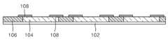
도 1을 참조하면, 본 발명의 제1 실시예에 의한 웨이퍼 레벨 적층형 패키지(100)의 제조방법은, 먼저 접착력을 갖는 캐리어(102) 위에 복수개의 제1 반도체 칩(104)을 탑재한다. 이때 상기 제1 반도체 칩(104)의 활성영역(A)은 위로 향하도록 캐리어(102)에 탑재하는 것이 적합하다. 상기 캐리어(102)는 표면에 빛 혹 은 열에 의해 접착력이 변하는 접착층(미도시)이 형성된 단단한 기판(hard substrate)인 것이 적합하다.Referring to FIG. 1, in the method of manufacturing the wafer-level stacked
도 2를 참조하면 상기 캐리어(102) 위에 탑재된 제1 반도체 칩(104)과 동일한 높이를 갖는 제1 봉지부(106)를 형성한다. 상기 제1 봉지부(106)를 형성하는 방법은 몰딩(molding), 프린팅(printing), 스핀 코팅(spin coating), 제팅(jetting) 중에서 선택된 하나의 방법으로 형성할 수 있다. 상기 방법중 몰딩 방식을 사용할 경우, 에폭시 몰드 컴파운드(EMC: Epoxy Mold Compound)를 제1 봉지부의 재질로 사용할 수 있다.Referring to FIG. 2, a
도 3을 참조하면, 상기 제1 봉지부(106)가 형성된 결과물 위에 제1 재배선 패턴(108)을 형성한다. 상기 제1 재배선 패턴(108)은 구리/금/니켈이 순차적으로 적층된 다층막인 것이 적합하다. 상기 제1 재배선 패턴(108)은 상기 제1 반도체 칩(104)의 본드패드(미도시)와 연결되어 상기 제1 봉지부(106)로 부채꼴 모양으로 확장된 패턴이다. 따라서 비록 제1 반도체 칩(104) 내에서 본드패드끼리의 간격이 좁게 설계되더라도, 상기 제1 재배선 패턴(108)을 통하여 상기 제1 봉지부(106) 위에서 부채꼴 모양으로 넓게 확장되기 때문에 본드패드 사이의 간격이 좁게 설계된 문제를 해결하면서 매우 효율적인 팬-아웃(fan-out) 구조를 달성할 수 있다.Referring to FIG. 3, a
여기서 반도체 패키지의 팬 아웃(fan-out) 구조란, 본드패드와 연결된 재배선 패턴이 반도체 칩의 크기보다 넓게 확장되어 재배치되는 것을 말하며, 팬-인(fan-in) 구조란, 반도체 칩의 넓이 한도에서 본드패드가 재배치되는 것을 말한다.Here, the fan-out structure of the semiconductor package means that the redistribution pattern connected to the bond pads is expanded and relocated wider than the size of the semiconductor chip. The fan-in structure is the width of the semiconductor chip. To the extent that bond pads are relocated.
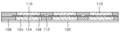
도 4 및 도 5를 참조하면, 상기 제1 재배치 패턴(108)이 형성된 상기 제1 반도체 칩(104) 위에 접착수단(124)을 사용하여 제2 반도체 칩(110)을 탑재한다. 이때 상기 제2 반도체 칩(110) 역시 본드패드가 있는 활성영역이 위로 향하도록 탑재되는 것이 적합하다. 계속해서 상기 제2 반도체 칩(110)의 가장자리에 상기 제2 반도체 칩(110)과 동일한 높이를 갖는 제2 봉지부(112)를 형성한다. 상기 제2 봉지부(112) 역시 상술한 제1 봉지부(106)와 동일한 방식으로 형성할 수 있다.4 and 5, the
도 6 내지 도 8을 참조하면, 상기 제2 봉지부(112)에 상기 제1 재배치 패턴(108)을 노출시키는 콘택홀(114)을 뚫는다. 상기 콘택홀(114)을 형성하는 방법은 레이저 드릴링(LASER drilling)과 같은 방법을 사용할 수 있으며, 기타 다른 방법을 통하여 형성할 수도 있다.6 to 8, a
이어서 상기 콘택홀(114)을 도전물질로 채워 비아 콘택(118)을 만들고, 상기 제2 반도체 칩(110) 및 상기 제2 봉지부(112) 위에 제2 재배선 패턴(116)을 만든다. 이때, 상기 제2 재배선 패턴(116) 역시 상기 제1 재배선 패턴과 동일한 모양인 것이 바람직하고, 상기 제2 반도체 칩(110)의 본드패드와 연결되어 제2 봉지부(112) 위에서 부채꼴 모양으로 확장된 형태인 것이 바람직하다. 이에 따라 상기 재1 반도체 칩(104) 및 제2 반도체 칩(110)은 제2 봉지부(112) 내부에 마련된 비아콘택(118)을 통해 전기적으로 서로 연결된다.Subsequently, the
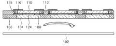
계속해서 상기 결과물에 열을 인가하거나 빛을 조사하여 상기 캐리어(102)에 존재하는 접착층의 접착력을 약화시켜 상기 캐리어(102)를 상기 제1 반도체 칩(104)의 밑면으로부터 떼어내어 제거한다.Subsequently, heat is applied to the resultant or irradiated with light to weaken the adhesive force of the adhesive layer existing on the
한편, 상기 캐리어(102)는 재질이 열전달 특성이 우수한 금속재질을 사용한 후, 위에서 설명된 것과 다르게 제거하지 않을 수도 있다. 이 경우, 상기 캐리어(102)는 상기 제1 반도체 칩(104)의 밑면을 보호하는 보호층의 역할을 수행할 수 있으며 이에 대해서는 추후 도 21을 참조하여 상세히 설명하기로 한다.On the other hand, the
또한 상기 제1 및 제2 반도체 칩(104, 110) 사이에 다른 반도체 칩, 다른 봉지부 및 다른 재배선 패턴을 형성하는 공정을 추가로 진행할 수 있으며, 이때 각각의 반도체 칩의 크기 및 두께는 서로 같거나 다르게 설계할 수 있다. 일 예로 4개의 반도체 칩을 적층할 경우, 4개의 반도체 칩을 서로 연결하는 비아 콘택(118)은 반도체 칩의 적층이 완전히 이루어지고 제2 봉지부(112)를 형성한 후, 한번에 콘택홀을 뚫어서 만들 수 있다. 또한 이를 변형하여 한 개의 반도체 칩이 적층되고 동일한 높이의 봉지부가 만들어진 후, 3회에 걸쳐서 콘택홀을 뚫고 내부를 도전물질로 매립하여 비아콘택(118)을 만들 수도 있다. 이에 대해서는 추후 도 16 내재 도 19에서 상세히 설명하기로 한다.In addition, a process of forming another semiconductor chip, another encapsulation portion, and another redistribution pattern between the first and
도 9를 참조하면, 상기 제2 재배선 패턴(116) 위에 돌출형 연결단자, 예컨대 솔더볼(120)이나 범프(bump)를 형성한다. 그 후, 블레이드(blade)를 사용한 절단공정인 싱귤레이션(singulation) 공정을 진행하여 낱개로 분리된 형태의 본 발명의 제1 실시예에 의한 웨이퍼 레벨 적층형 패키지(100)를 얻는다.Referring to FIG. 9, a protruding connection terminal, for example, a
도 10은 본 발명의 제1 실시예에 의하여 제조된 웨이퍼 레벨 적층형 패키지를 보여주는 단면도이다.10 is a cross-sectional view showing a wafer level stacked package manufactured according to the first embodiment of the present invention.
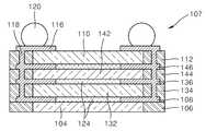
도 10을 참조하면, 본 발명의 제1 실시예에 의한 봉지부를 통하여 재배선을 달성하는 웨이퍼 레벨 적층형 패키지(100)는, 활성영역이 위로 향한 제1 반도체 칩과, 상기 제1 반도체 칩(104)의 가장자리를 따라 형성된 제1 봉지부(106)와, 상기 제1 반도체 칩(104)의 상부에서 상기 제1 반도체 칩(104)의 본드패드와 연결되어 상기 제1 봉지부(106) 위로 연장된 제1 재배선 패턴(108)을 포함한다.Referring to FIG. 10, a wafer level stacked
또한 본 발명의 제1 실시예에 의한 봉지부를 통하여 재배선을 달성하는 웨이퍼 레벨 적층형 패키지(100)는, 상기 제1 반도체 칩(104) 위에 접착수단(124)을 통하여 활성영역이 위로 향하도록 탑재된 제2 반도체 칩(110)과, 상기 제1 봉지부(106) 위에서 상기 제2 반도체 칩(110)의 가장자리를 따라 형성된 제2 봉지부(112)와, 상기 제2 반도체 칩(110)의 상부에서 상기 제2 반도체 칩(110)의 본드패드와 연결되어 상기 제2 봉지부(112) 위로 연장된 제2 재배선 패턴(116)과, 상기 제2 봉지부(112) 내부에서 상기 제1 재배선 패턴(108)과 상기 제2 재배선 패턴(116)을 연결하는 비아콘택(118) 및 상기 제2 재배선 패턴(116) 위에 부착된 돌출형 연결단자(120)인 솔더볼을 포함하여 구성된다. 이때, 상기 돌출형 연결단자(120)는 솔더볼 대신에 범프(bump)로 대치될 수 있다.In addition, the wafer-level
도 11 내지 도 15는 본 발명의 제2 실시예에 의한 웨이퍼 레벨 적층형 패키지의 제조방법을 설명하기 위한 단면도들이다.11 to 15 are cross-sectional views illustrating a method of manufacturing a wafer-level stacked package according to a second embodiment of the present invention.
도 11 내지 도 15를 참조하면, 먼저 접착력을 갖는 캐리어(202) 위에 반도체 칩의 활성영역(A)이 밑으로 향하도록 제1 반도체 칩(204)을 탑재한다. 이어서 상기 제1 반도체 칩(204)의 측면과 밑면을 충분히 덮는 구조의 제1 봉지부(206)를 형성한다. 상기 제1 봉지부(206)는 몰딩 공정을 통하여 형성할 수 있으며, 그 재질 은 에폭시 몰드 컴파운드(EMC)를 사용할 수 있다.11 to 15, first, the
그 후, 상기 캐리어(202)를 상기 제1 반도체 칩(204) 및 제1 봉지부(206)로부터 떼어내어 제거하고, 제1 봉지부(206)가 형성된 결과물을 뒤집는다. 그 후, 상기 제1 반도체 칩(204)의 활성영역 및 제1 봉지부(206) 위에 제1 재배선 패턴(208)을 형성한다. 상기 제1 재배선 패턴(208) 역시 상술한 제1 실시예와 동일하게 부채꼴 모양으로 확장되는 형태로서 본 발명의 제2 실시예에 의한 웨이퍼 레벨 적층형 패키지에서 본드패드의 파인 피치 문제를 해결하고, 팬-아웃 구조를 실현할 수 있는 수단이 된다.Thereafter, the
계속해서 상기 제1 반도체 칩(204) 위에 접착수단(224)을 사용하여 제2 반도체 칩(210)을 탑재한다. 이때에는 상기 제2 반도체 칩(210)의 활성영역이 위로 향하도록 탑재되는 것이 적합하다. 그 후 상기 제2 반도체 칩(210)과 동일한 높이를 갖는 제2 봉지부(212)를 형성한다. 그리고 상기 제2 봉지부(212) 내부에 비아콘택(218)을 형성하고, 상기 비아콘택(218)을 제2 반도체 칩(210) 및 제2 봉지부(212) 위에 있는 제2 재배선 패턴(216)과 연결하여 상기 제1 및 제2 반도체 칩(204, 210)을 전기적으로 서로 연결시킨다. 마지막으로 상기 제2 재배선 패턴(216) 위에 솔더볼(220)을 부착하고 싱귤레이션 공정을 진행하여 본 발명의 제2 실시예에 의한 봉지부를 통하여 재배선을 달성하는 웨이퍼 레벨 적층형 패키지(200)를 낱개로 분리시킨다.Subsequently, the
한편 본 발명의 제2 실시예에 의한 웨이퍼 레벨 적층형 패키지(200) 패키지는, 상기 제1 실시예에서 소개된 웨이퍼 레벨 적층형 패키지(100)와 유사한 구조를 갖으나, 제1 봉지부(206)가 제1 반도체 칩(204)과 동일한 높이가 아니고 제1 반도체 칩(204)의 밑면을 완전히 덮은 구조상의 차이점을 갖는다.On the other hand, the wafer level stacked
도 16은 본 발명의 제1 실시예에 의한 웨이퍼 레벨 적층형 패키지의 제1 변형예이다.16 is a first modification of the wafer level stacked package according to the first embodiment of the present invention.
도 16을 참조하면, 상기 제1 실시예에서는 반도체 칩의 적층 개수가 2개(104, 110)였으나, 본 변형예에서는 중간에 2개의 다른 반도체 칩(132, 142)과 2개의 다른 봉지부(134, 144) 및 2개의 다른 재배선 패턴(136, 146)을 추가로 삽입한 경우이다.Referring to FIG. 16, in the first embodiment, the number of stacking of semiconductor chips is two (104, 110), but in the present modification, two
물론 도면에는 4개의 반도체 칩(104, 110, 132, 142)을 적층하는 형태이지만 상기 반도체 칩의 개수는 필요에 따라 추가하거나 뺄 수도 있다. 이러한 구조의 웨이퍼 레벨 적층형 패키지(101)는 반도체 메모리와 같은 동일 기능을 갖는 반도체 칩들을 적층하여 반도체 패키지로 만드는데 적용되면 유리하다.Of course, four
한편, 상기 웨이퍼 레벨 적층형 패키지(101)의 제조방법에 있어서, 상기 비아콘택(118)은 4개의 반도체 칩과 4개의 봉지부를 모두 형성한 후, 한번에 콘택홀을 뚫어 그 내부를 도전물질로 채워서 만들 수 있고, 이를 변형시켜 하나의 반도체 칩과 봉지부가 적층될 때마다 개별적으로 콘택홀을 뚫어 비아콘택(118)을 형성할 수 있다. 나머지 구조 및 제조방법은 상술한 제1 실시예에서 이미 설명되었기 때문에 중복을 피하여 설명을 생략한다.Meanwhile, in the method of manufacturing the wafer-level
도 17은 본 발명의 제1 실시예에 의한 웨이퍼 레벨 적층형 패키지의 제2 변형예이다.17 is a second modification of the wafer level stacked package according to the first embodiment of the present invention.
도 17을 참조하면, 상술한 본 발명의 제1 실시예에 의한 웨이퍼 레벨 적층형 패키지(100)에서는 반도체 칩의 크기는 문제되지 않았다. 그러나 본 변형예와 같이 반도체 칩(104, 132, 142, 110)의 크기가 각각 다른 것을 적층하고 하나의 비아콘택(118)을 통하여 전기적으로 서로 연결하는 형태로 변형이 가능하다. 이때 상기 반도체 칩(104, 132, 142, 110)들은 마이크로 컨트롤러(Micro controller), 메모리 및 로직과 같이 각각 다른 기능을 수행하는 반도체 칩일 수 있다. 이러한 구조의 웨이퍼 레벨 적층형 패키지(103)는 SIP(System In Package)와 같은 반도체 패키지에 적용시킬 수 있다.Referring to FIG. 17, in the wafer-level
도 18은 본 발명의 제1 실시예에 의한 웨이퍼 레벨 적층형 패키지의 제3 변형예이다.18 is a third modification of the wafer level stacked package according to the first embodiment of the present invention.
도 18을 참조하면, 상기 도17에서는 서로 다른 크기를 갖는 4개의 반도체 칩(104, 132, 142, 110)이 하나의 상하 연결통로인 비아콘택(118)을 통하여 상부로 연결되었다. 그러나 상기 반도체 칩들이 각각 서로 다른 기능을 수행하고, 회로가 동작하는 통로가 복잡할 경우, 본 변형예에 의한 웨이퍼 레벨 적층형 패키지(105)와 같이 복수개의 비아콘택(118A, 118B, 118C, 118D)을 갖도록 상하 연결통로를 변형시킬 수 있다.Referring to FIG. 18, four
도 19는 본 발명의 제1 실시예에 의한 웨이퍼 레벨 적층형 패키지의 제4 변형예이다.19 is a fourth modification of the wafer-level stacked package according to the first embodiment of the present invention.
도 19를 참조하면, 본 발명의 제1 실시예에 의한 웨이퍼 레벨 적층형 패키지(100)는 사용되는 반도체 칩(104, 110)의 두께가 동일하였으나, 본 변형예에 의 한 웨이퍼 레벨 적층형 패키지(107)와 같이 전체적인 두께를 얇게 하기 위하여 두께가 서로 다른 반도체 칩(104, 132, 142, 110)을 적층하는 형태로 변형시킬 수 있다. 물론 이때 상기 반도체 칩(104, 132, 142, 110)의 측면에 형성되는 봉지부(106, 134, 144, 112)의 두께도 상기 반도체 칩(104, 132, 142, 110)의 두께에 비례하여 조정된다.Referring to FIG. 19, the wafer level stacked
도 20은 본 발명의 제1 실시예에 의한 웨이퍼 레벨 적층형 패키지의 제5 변형예이다.20 is a fifth modified example of the wafer-level stacked package according to the first embodiment of the present invention.
도 20을 참조하면, 본 발명의 제1 실시예에 의한 웨이퍼 레벨 적층형 패키지(100)는, 제1 반도체 칩으로 하나의 반도체 칩(104)을 사용하였으나, 본 변형예에 의한 웨이퍼 레벨 적층형 패키지(109)는 하나 이상 두 개의 반도체 칩(104A, 104B)을 사용하는 특징이 있다. 상기 두 개의 반도체 칩(104A, 104B)은 도면에서는 크기가 서로 다른 것이지만, 이는 동일 기능을 수행하고 크기가 서로 같은 반도체 칩으로 대치시킬 수도 있다. 또한 본 변형예는 제1 반도체 칩을 하나 이상으로 만드는 방식이었으나, 이는 중간 혹은 상부에 배치되는 반도체 칩(110)을 두 개 이상 배치하는 형태로 변형이 가능하다.Referring to FIG. 20, the wafer level stacked
도 21은 본 발명의 제1 실시예에 의한 웨이퍼 레벨 적층형 패키지의 제6 변형예이다.21 is a sixth modification of the wafer-level stacked package according to the first embodiment of the present invention.
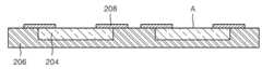
도 21을 참조하면, 본 발명의 제1 실시예에 의한 웨이퍼 레벨 적층형 패키지(100)는 제1 반도체 칩(104) 하부에 별도의 보호층이 없는 구조이다. 그러나 본 변형예에 의한 웨이퍼 레벨 적층형 패키지(111)는, 제1 반도체 칩(104) 및 제1 봉 지부(104) 아래에 별도의 보호층(126)이 만들어지는 특징이 있다. 이러한 보호층(126)은 제조공정에서 사용된 캐리어(도1의 102)를 사용하여 만들 수 있고, 별도로 열전달 특성이 우수한 단단한 기판을 부착하여 만들 수 있다.Referring to FIG. 21, the wafer-level
따라서 상기 보호층(126)은 웨이퍼 레벨 적층형 패키지(111)의 하단부에서 물리적 충격이 가해지는 것을 완충시키는 기계적 보호수단이 됨과 동시에, 열전달 특성이 우수한 구리 혹은 알루미늄과 같은 금속을 그 재질로 사용할 경우, 상기 제1 및 제2 반도체 칩(104, 110)에서 발생하는 열을 외부로 발산시키는 통로의 역할을 할 수 있는 장점이 있다.Therefore, the
도 22는 본 발명의 제3 실시예에 의한 봉지부를 통하여 재배선을 달성하는 웨이퍼 레벨 적층형 패키지를 설명하기 위한 단면도이다.FIG. 22 is a cross-sectional view for describing a wafer level stacked package that achieves redistribution through an encapsulation part according to a third exemplary embodiment of the present invention.
도 22를 참조하면, 본 발명의 제3 실시예에 의한 웨이퍼 레벨 적층형 패키지(300)는, 상술한 제1 및 제2 실시예의 특징과 함께 내부에 범프(312)를 통하여 하부 반도체 칩에 연결되는 하나 이상의 반도체 칩(310)을 더 포함하는 특징이 있다.Referring to FIG. 22, a wafer level stacked
본 발명의 제3 실시예에 의한 웨이퍼 레벨 적층형 패키지(300)의 구성은, 활성영역이 위로 향한 제1 반도체 칩(304)과, 상기 제1 반도체 칩(304)의 가장자리를 따라 형성된 제1 봉지부(encapsulation portion, 306)와, 상기 제1 반도체 칩(304)의 상부에서 상기 제1 반도체 칩(304)의 본드패드(미도시)와 연결되어 상기 제1 봉지부(306) 위로 연장된 제1 재배선 패턴(308)과, 상기 제1 반도체 칩(304) 위에 범프(312)를 통하여 전기적으로 연결되고 상기 제1 반도체 칩(304)보다 크기가 작은 제2 반도체 칩(310) 및 상기 제2 반도체 칩(310)의 가장자리를 따라 형성된 제2 봉지부(314)를 포함한다.The wafer-level
또한, 본 발명의 제3 실시예에 의한 웨이퍼 레벨 적층형 패키지(300)는, 상기 제2 반도체 칩(310) 위에 접착수단(316)을 통하여 활성영역이 위로 향하도록 탑재된 제3 반도체 칩(318)과, 상기 제2 봉지부(314) 위에서 상기 제3 반도체 칩(318)의 가장자리를 따라 형성된 제3 봉지부(320)와, 상기 제3 반도체 칩(318)의 상부에서 상기 제3 반도체 칩(318)의 본드패드와 연결되어 상기 제3 봉지부(320) 위로 연장된 제3 재배선 패턴(324)과, 상기 제2 및 제3 봉지부(314, 320) 내부에서 상기 제1 재배선 패턴(308)과 상기 제3 재배선 패턴(324)을 연결하는 비아콘택(322) 및 상기 제3 재배선 패턴(324) 위에 부착된 돌출형 연결단자(326)인 솔더볼을 포함하여 이루어진다.In addition, in the wafer-level
또한, 본 발명의 제3 실시예에 의한 웨이퍼 레벨 적층형 패키지(300)는, 도 21과 같이 상기 제1 반도체 칩(304) 아래에 별도의 보호층을 추가로 포함할 수도 있다.In addition, the wafer-level
이하, 본 발명의 제3 실시예에 의한 웨이퍼 레벨 적층형 패키지(300)의 제조방법에 관해 설명한다.Hereinafter, a method of manufacturing the wafer level stacked
먼저, 표면에 접착력을 갖는 캐리어 위에 복수개의 제1 반도체 칩(304)을 활성영역이 위로 향하도록 탑재한다. 그 후, 상기 캐리어 위에 상기 제1 반도체 칩(304)과 동일한 높이의 제1 봉지부(306)를 형성한다. 이어서 상기 제1 반도체 칩(304)의 일부 본드패드와 연결되고 상기 제1 봉지부(306)로 확장되는 제1 재배선 패턴(308)을 형성하고, 상기 제1 재배선 패턴(308)이 연결되지 않은 제1 반도체 칩(304)의 나머지 본드패드와 범프(312)를 통해 연결되고 제1 반도체 칩(304)보다 크기가 작은 제2 반도체 칩(310)을 탑재하고, 상기 제 2 반도체 칩(310)과 동일한 높이의 제2 봉지부(314)를 상기 제1 봉지부(306) 위에 형성한다.First, a plurality of
계속해서, 상기 제2 봉지부(314)가 형성된 상기 제2 반도체 칩(310) 위에 접착수단(316)을 사용하여 제3 반도체 칩(318)을 활성영역이 위로 향하도록 탑재하고, 상기 제2 봉지부(314) 위에 상기 제3 반도체 칩(318)과 동일한 높이의 제3 봉지부(320)를 형성한다. 그리고 상기 제2 및 제3 봉지부(314, 320)에 상기 제1 재배선 패턴(308)을 노출시키는 콘택홀을 형성하고 내부를 도전물질로 채워 비아콘택(322)을 형성하고, 상기 제3 반도체 칩(318)의 본드패드와 연결되고 상기 제3 봉지부(320)로 확장되어 상기 비아콘택(322)과 전기적으로 연결되는 제3 재배선 패턴(324)을 형성한다.Subsequently, a
마지막으로 상기 제3 재배선 패턴(324)에 솔더볼(326)과 같은 돌출형 연결단자를 부착하고, 싱귤레이션 공정(singulation)을 통하여 본 발명의 제3 실시예에 의한 웨이퍼 레벨 적층형 패키지(300)를 낱개로 분리시킨다.Finally, the protruding connection terminal such as the
도 23은 본 발명의 제1 실시예의 변형예에 의한 웨이퍼 레벨 적층형 패키지가 응용되는 것을 보여주는 단면도이다.Fig. 23 is a cross-sectional view showing the application of a wafer level stacked package according to a modification of the first embodiment of the present invention.
도 23을 참조하면, 본 응용예에서는 상술한 제1 내지 제3 실시예에서 소개된 웨이퍼 레벨 적층형 패키지가 한 개 이상 수직으로 다시 적층될 수 있음을 보여준다. 즉, 높이에 제한을 받지 않고, 한정된 면적내에서 많은 반도체 회로를 형성해 야 할 경우, 본 응용예와 같이 하나 이상의 웨이퍼 레벨 적층형 패키지(105, 107)를 수직방향으로 적층시켜 패키지 모듈을 구현할 수 있다.Referring to FIG. 23, in the present application example, one or more wafer level stacked packages introduced in the above-described first to third embodiments may be stacked again vertically. In other words, when a large number of semiconductor circuits are to be formed within a limited area without being limited in height, a package module may be implemented by stacking one or more wafer level stacked
본 발명은 상기한 실시예에 한정되지 않으며, 본 발명이 속한 기술적 사상 내에서 당 분야의 통상의 지식을 가진 자에 의해 많은 변형이 가능함이 명백하다.The present invention is not limited to the above embodiments, and it is apparent that many modifications can be made by those skilled in the art within the technical spirit to which the present invention belongs.
도 1 내지 도 9는 본 발명의 제1 실시예에 의한 봉지부를 통하여 재배선을 달성하는 웨이퍼 레벨 적층형 패키지의 제조방법을 설명하기 위한 단면도들이다.1 to 9 are cross-sectional views illustrating a method of manufacturing a wafer level stacked package for achieving redistribution through an encapsulation part according to a first embodiment of the present invention.
도 10은 본 발명의 제1 실시예에 의하여 제조된 웨이퍼 레벨 적층형 패키지를 보여주는 단면도이다.10 is a cross-sectional view showing a wafer level stacked package manufactured according to the first embodiment of the present invention.
도 11 내지 도 15는 본 발명의 제2 실시예에 의한 봉지부를 통하여 재배선을 달성하는 웨이퍼 레벨 적층형 패키지의 제조방법을 설명하기 위한 단면도들이다.11 to 15 are cross-sectional views illustrating a method of manufacturing a wafer level stacked package that achieves redistribution through an encapsulation part according to a second embodiment of the present invention.
도 16은 본 발명의 제1 실시예에 의한 웨이퍼 레벨 적층형 패키지의 제1 변형예이다.16 is a first modification of the wafer level stacked package according to the first embodiment of the present invention.
도 17은 본 발명의 제1 실시예에 의한 웨이퍼 레벨 적층형 패키지의 제2 변형예이다.17 is a second modification of the wafer level stacked package according to the first embodiment of the present invention.
도 18은 본 발명의 제1 실시예에 의한 웨이퍼 레벨 적층형 패키지의 제3 변형예이다.18 is a third modification of the wafer level stacked package according to the first embodiment of the present invention.
도 19는 본 발명의 제1 실시예에 의한 웨이퍼 레벨 적층형 패키지의 제4 변형예이다.19 is a fourth modification of the wafer-level stacked package according to the first embodiment of the present invention.
도 20은 본 발명의 제1 실시예에 의한 웨이퍼 레벨 적층형 패키지의 제5 변형예이다.20 is a fifth modified example of the wafer-level stacked package according to the first embodiment of the present invention.
도 21은 본 발명의 제1 실시예에 의한 웨이퍼 레벨 적층형 패키지의 제6 변형예이다.21 is a sixth modification of the wafer-level stacked package according to the first embodiment of the present invention.
도 22는 본 발명의 제3 실시예에 의한 봉지부를 통하여 재배선을 달성하는 웨이퍼 레벨 적층형 패키지를 설명하기 위한 단면도이다.FIG. 22 is a cross-sectional view for describing a wafer level stacked package that achieves redistribution through an encapsulation part according to a third exemplary embodiment of the present invention.
도 23은 본 발명의 제1 실시예의 변형예에 의한 웨이퍼 레벨 적층형 패키지가 응용되는 것을 보여주는 단면도이다.Fig. 23 is a cross-sectional view showing the application of a wafer level stacked package according to a modification of the first embodiment of the present invention.
Claims (38)
Translated fromKoreanPriority Applications (3)
| Application Number | Priority Date | Filing Date | Title |
|---|---|---|---|
| KR1020070070775AKR20090007120A (en) | 2007-07-13 | 2007-07-13 | Wafer level laminated package to achieve redistribution through encapsulation and manufacturing method |
| TW097122404ATW200903755A (en) | 2007-07-13 | 2008-06-16 | Wafer level stacked package having via contact in encapsulation portion and manufacturing method thereof |
| US12/216,095US20090014876A1 (en) | 2007-07-13 | 2008-06-30 | Wafer level stacked package having via contact in encapsulation portion and manufacturing method thereof |
Applications Claiming Priority (1)
| Application Number | Priority Date | Filing Date | Title |
|---|---|---|---|
| KR1020070070775AKR20090007120A (en) | 2007-07-13 | 2007-07-13 | Wafer level laminated package to achieve redistribution through encapsulation and manufacturing method |
Publications (1)
| Publication Number | Publication Date |
|---|---|
| KR20090007120Atrue KR20090007120A (en) | 2009-01-16 |
Family
ID=40252405
Family Applications (1)
| Application Number | Title | Priority Date | Filing Date |
|---|---|---|---|
| KR1020070070775AWithdrawnKR20090007120A (en) | 2007-07-13 | 2007-07-13 | Wafer level laminated package to achieve redistribution through encapsulation and manufacturing method |
Country Status (3)
| Country | Link |
|---|---|
| US (1) | US20090014876A1 (en) |
| KR (1) | KR20090007120A (en) |
| TW (1) | TW200903755A (en) |
Cited By (6)
| Publication number | Priority date | Publication date | Assignee | Title |
|---|---|---|---|---|
| KR20110108136A (en)* | 2010-03-26 | 2011-10-05 | 삼성전자주식회사 | A semiconductor housing package, a semiconductor package structure including the semiconductor housing package, and a processor based system including the semiconductor package structure |
| KR101219086B1 (en)* | 2011-03-07 | 2013-01-11 | (주) 윈팩 | Package module |
| KR101478508B1 (en)* | 2012-08-09 | 2015-01-02 | 앰코 테크놀로지 코리아 주식회사 | Wafer level fan out package and method for manufacturing the same |
| US9202716B2 (en) | 2011-12-09 | 2015-12-01 | Samsung Electronics Co., Ltd. | Methods of fabricating fan-out wafer level packages and packages formed by the methods |
| KR20160064122A (en)* | 2013-09-26 | 2016-06-07 | 베시 네덜란드 비.브이. | Method for moulding and surface processing electronic components and electronic component produced with this method |
| KR20170127061A (en)* | 2013-09-27 | 2017-11-20 | 인텔 코포레이션 | Method for interconnecting stacked semiconductor devices |
Families Citing this family (70)
| Publication number | Priority date | Publication date | Assignee | Title |
|---|---|---|---|---|
| KR101313391B1 (en) | 2004-11-03 | 2013-10-01 | 테세라, 인코포레이티드 | Stacked packaging improvements |
| US8058101B2 (en) | 2005-12-23 | 2011-11-15 | Tessera, Inc. | Microelectronic packages and methods therefor |
| US8482111B2 (en) | 2010-07-19 | 2013-07-09 | Tessera, Inc. | Stackable molded microelectronic packages |
| US9159708B2 (en) | 2010-07-19 | 2015-10-13 | Tessera, Inc. | Stackable molded microelectronic packages with area array unit connectors |
| US8283754B2 (en)* | 2010-08-13 | 2012-10-09 | Taiwan Semiconductor Manufacturing Company, Ltd. | Seal ring structure with metal pad |
| KR101075241B1 (en) | 2010-11-15 | 2011-11-01 | 테세라, 인코포레이티드 | Microelectronic package with terminals in dielectric member |
| US20120146206A1 (en) | 2010-12-13 | 2012-06-14 | Tessera Research Llc | Pin attachment |
| US9170744B1 (en) | 2011-04-06 | 2015-10-27 | P4tents1, LLC | Computer program product for controlling a flash/DRAM/embedded DRAM-equipped system |
| US9158546B1 (en) | 2011-04-06 | 2015-10-13 | P4tents1, LLC | Computer program product for fetching from a first physical memory between an execution of a plurality of threads associated with a second physical memory |
| US9432298B1 (en) | 2011-12-09 | 2016-08-30 | P4tents1, LLC | System, method, and computer program product for improving memory systems |
| US8930647B1 (en) | 2011-04-06 | 2015-01-06 | P4tents1, LLC | Multiple class memory systems |
| US9164679B2 (en) | 2011-04-06 | 2015-10-20 | Patents1, Llc | System, method and computer program product for multi-thread operation involving first memory of a first memory class and second memory of a second memory class |
| US9176671B1 (en) | 2011-04-06 | 2015-11-03 | P4tents1, LLC | Fetching data between thread execution in a flash/DRAM/embedded DRAM-equipped system |
| US8618659B2 (en) | 2011-05-03 | 2013-12-31 | Tessera, Inc. | Package-on-package assembly with wire bonds to encapsulation surface |
| KR101128063B1 (en) | 2011-05-03 | 2012-04-23 | 테세라, 인코포레이티드 | Package-on-package assembly with wire bonds to encapsulation surface |
| US9417754B2 (en) | 2011-08-05 | 2016-08-16 | P4tents1, LLC | User interface system, method, and computer program product |
| US8836136B2 (en) | 2011-10-17 | 2014-09-16 | Invensas Corporation | Package-on-package assembly with wire bond vias |
| CN102344110B (en)* | 2011-10-31 | 2015-07-15 | 嘉盛半导体(苏州)有限公司 | Quad flat non-leaded package structure and method of micro electro mechanical system device |
| US8946757B2 (en) | 2012-02-17 | 2015-02-03 | Invensas Corporation | Heat spreading substrate with embedded interconnects |
| US9349706B2 (en) | 2012-02-24 | 2016-05-24 | Invensas Corporation | Method for package-on-package assembly with wire bonds to encapsulation surface |
| US8372741B1 (en) | 2012-02-24 | 2013-02-12 | Invensas Corporation | Method for package-on-package assembly with wire bonds to encapsulation surface |
| US8835228B2 (en) | 2012-05-22 | 2014-09-16 | Invensas Corporation | Substrate-less stackable package with wire-bond interconnect |
| KR101985236B1 (en) | 2012-07-10 | 2019-06-03 | 삼성전자주식회사 | Multi-chip package and method of manufacturing the same |
| US9391008B2 (en) | 2012-07-31 | 2016-07-12 | Invensas Corporation | Reconstituted wafer-level package DRAM |
| US9136213B2 (en) | 2012-08-02 | 2015-09-15 | Infineon Technologies Ag | Integrated system and method of making the integrated system |
| US9502390B2 (en) | 2012-08-03 | 2016-11-22 | Invensas Corporation | BVA interposer |
| US9129959B2 (en)* | 2012-08-21 | 2015-09-08 | Infineon Technologies Ag | Method for manufacturing an electronic module and an electronic module |
| KR101999262B1 (en) | 2012-09-12 | 2019-07-12 | 삼성전자주식회사 | Semiconductor Package and method for fabricating the same |
| US9721920B2 (en)* | 2012-10-19 | 2017-08-01 | Infineon Technologies Ag | Embedded chip packages and methods for manufacturing an embedded chip package |
| US8975738B2 (en) | 2012-11-12 | 2015-03-10 | Invensas Corporation | Structure for microelectronic packaging with terminals on dielectric mass |
| US8878353B2 (en) | 2012-12-20 | 2014-11-04 | Invensas Corporation | Structure for microelectronic packaging with bond elements to encapsulation surface |
| US9136254B2 (en) | 2013-02-01 | 2015-09-15 | Invensas Corporation | Microelectronic package having wire bond vias and stiffening layer |
| US8890284B2 (en)* | 2013-02-22 | 2014-11-18 | Infineon Technologies Ag | Semiconductor device |
| US9034696B2 (en) | 2013-07-15 | 2015-05-19 | Invensas Corporation | Microelectronic assemblies having reinforcing collars on connectors extending through encapsulation |
| US9023691B2 (en) | 2013-07-15 | 2015-05-05 | Invensas Corporation | Microelectronic assemblies with stack terminals coupled by connectors extending through encapsulation |
| US8883563B1 (en) | 2013-07-15 | 2014-11-11 | Invensas Corporation | Fabrication of microelectronic assemblies having stack terminals coupled by connectors extending through encapsulation |
| US9167710B2 (en) | 2013-08-07 | 2015-10-20 | Invensas Corporation | Embedded packaging with preformed vias |
| US9685365B2 (en) | 2013-08-08 | 2017-06-20 | Invensas Corporation | Method of forming a wire bond having a free end |
| US20150076714A1 (en) | 2013-09-16 | 2015-03-19 | Invensas Corporation | Microelectronic element with bond elements to encapsulation surface |
| US9082753B2 (en) | 2013-11-12 | 2015-07-14 | Invensas Corporation | Severing bond wire by kinking and twisting |
| US9087815B2 (en) | 2013-11-12 | 2015-07-21 | Invensas Corporation | Off substrate kinking of bond wire |
| US9263394B2 (en) | 2013-11-22 | 2016-02-16 | Invensas Corporation | Multiple bond via arrays of different wire heights on a same substrate |
| US9379074B2 (en) | 2013-11-22 | 2016-06-28 | Invensas Corporation | Die stacks with one or more bond via arrays of wire bond wires and with one or more arrays of bump interconnects |
| US9583456B2 (en) | 2013-11-22 | 2017-02-28 | Invensas Corporation | Multiple bond via arrays of different wire heights on a same substrate |
| US9184128B2 (en)* | 2013-12-13 | 2015-11-10 | Taiwan Semiconductor Manufacturing Company, Ltd. | 3DIC package and methods of forming the same |
| US9583411B2 (en) | 2014-01-17 | 2017-02-28 | Invensas Corporation | Fine pitch BVA using reconstituted wafer with area array accessible for testing |
| US9214454B2 (en) | 2014-03-31 | 2015-12-15 | Invensas Corporation | Batch process fabrication of package-on-package microelectronic assemblies |
| US10381326B2 (en) | 2014-05-28 | 2019-08-13 | Invensas Corporation | Structure and method for integrated circuits packaging with increased density |
| US9646917B2 (en) | 2014-05-29 | 2017-05-09 | Invensas Corporation | Low CTE component with wire bond interconnects |
| US9412714B2 (en) | 2014-05-30 | 2016-08-09 | Invensas Corporation | Wire bond support structure and microelectronic package including wire bonds therefrom |
| US9735084B2 (en) | 2014-12-11 | 2017-08-15 | Invensas Corporation | Bond via array for thermal conductivity |
| US9888579B2 (en) | 2015-03-05 | 2018-02-06 | Invensas Corporation | Pressing of wire bond wire tips to provide bent-over tips |
| US9502372B1 (en) | 2015-04-30 | 2016-11-22 | Invensas Corporation | Wafer-level packaging using wire bond wires in place of a redistribution layer |
| US9761554B2 (en) | 2015-05-07 | 2017-09-12 | Invensas Corporation | Ball bonding metal wire bond wires to metal pads |
| US9601467B1 (en)* | 2015-09-03 | 2017-03-21 | Invensas Corporation | Microelectronic package with horizontal and vertical interconnections |
| US20170098629A1 (en)* | 2015-10-05 | 2017-04-06 | Mediatek Inc. | Stacked fan-out package structure |
| US9490222B1 (en) | 2015-10-12 | 2016-11-08 | Invensas Corporation | Wire bond wires for interference shielding |
| US10490528B2 (en) | 2015-10-12 | 2019-11-26 | Invensas Corporation | Embedded wire bond wires |
| US10332854B2 (en) | 2015-10-23 | 2019-06-25 | Invensas Corporation | Anchoring structure of fine pitch bva |
| US10181457B2 (en) | 2015-10-26 | 2019-01-15 | Invensas Corporation | Microelectronic package for wafer-level chip scale packaging with fan-out |
| US10043779B2 (en) | 2015-11-17 | 2018-08-07 | Invensas Corporation | Packaged microelectronic device for a package-on-package device |
| US9659848B1 (en) | 2015-11-18 | 2017-05-23 | Invensas Corporation | Stiffened wires for offset BVA |
| KR102420125B1 (en) | 2015-12-10 | 2022-07-13 | 삼성전자주식회사 | Semiconductor package and method of fabricating the same |
| US9984992B2 (en) | 2015-12-30 | 2018-05-29 | Invensas Corporation | Embedded wire bond wires for vertical integration with separate surface mount and wire bond mounting surfaces |
| US9935075B2 (en) | 2016-07-29 | 2018-04-03 | Invensas Corporation | Wire bonding method and apparatus for electromagnetic interference shielding |
| WO2018086395A1 (en)* | 2016-11-08 | 2018-05-17 | 华进半导体封装先导技术研发中心有限公司 | Semiconductor memory, semiconductor storage module and manufacturing method therefor |
| US10299368B2 (en) | 2016-12-21 | 2019-05-21 | Invensas Corporation | Surface integrated waveguides and circuit structures therefor |
| US11145566B2 (en)* | 2020-02-10 | 2021-10-12 | Xilinx, Inc. | Stacked silicon package assembly having thermal management |
| CN111463138B (en)* | 2020-04-20 | 2021-05-18 | 长江存储科技有限责任公司 | Semiconductor device and method of making the same |
| CN117713689A (en)* | 2023-12-29 | 2024-03-15 | 合肥矽迈微电子科技有限公司 | A crystal oscillator and its packaging method |
Family Cites Families (6)
| Publication number | Priority date | Publication date | Assignee | Title |
|---|---|---|---|---|
| US5239448A (en)* | 1991-10-28 | 1993-08-24 | International Business Machines Corporation | Formulation of multichip modules |
| US6380555B1 (en)* | 1999-12-24 | 2002-04-30 | Micron Technology, Inc. | Bumped semiconductor component having test pads, and method and system for testing bumped semiconductor components |
| TW544882B (en)* | 2001-12-31 | 2003-08-01 | Megic Corp | Chip package structure and process thereof |
| CN1577819A (en)* | 2003-07-09 | 2005-02-09 | 松下电器产业株式会社 | Circuit board with in-built electronic component and method for manufacturing the same |
| US7459781B2 (en)* | 2003-12-03 | 2008-12-02 | Wen-Kun Yang | Fan out type wafer level package structure and method of the same |
| TWI263313B (en)* | 2005-08-15 | 2006-10-01 | Phoenix Prec Technology Corp | Stack structure of semiconductor component embedded in supporting board |
- 2007
- 2007-07-13KRKR1020070070775Apatent/KR20090007120A/ennot_activeWithdrawn
- 2008
- 2008-06-16TWTW097122404Apatent/TW200903755A/enunknown
- 2008-06-30USUS12/216,095patent/US20090014876A1/ennot_activeAbandoned
Cited By (8)
| Publication number | Priority date | Publication date | Assignee | Title |
|---|---|---|---|---|
| KR20110108136A (en)* | 2010-03-26 | 2011-10-05 | 삼성전자주식회사 | A semiconductor housing package, a semiconductor package structure including the semiconductor housing package, and a processor based system including the semiconductor package structure |
| KR101219086B1 (en)* | 2011-03-07 | 2013-01-11 | (주) 윈팩 | Package module |
| US9202716B2 (en) | 2011-12-09 | 2015-12-01 | Samsung Electronics Co., Ltd. | Methods of fabricating fan-out wafer level packages and packages formed by the methods |
| KR101478508B1 (en)* | 2012-08-09 | 2015-01-02 | 앰코 테크놀로지 코리아 주식회사 | Wafer level fan out package and method for manufacturing the same |
| KR20160064122A (en)* | 2013-09-26 | 2016-06-07 | 베시 네덜란드 비.브이. | Method for moulding and surface processing electronic components and electronic component produced with this method |
| KR20170127061A (en)* | 2013-09-27 | 2017-11-20 | 인텔 코포레이션 | Method for interconnecting stacked semiconductor devices |
| US11024607B2 (en) | 2013-09-27 | 2021-06-01 | Intel Corporation | Method for interconnecting stacked semiconductor devices |
| US12033983B2 (en) | 2013-09-27 | 2024-07-09 | Intel Corporation | Method for interconnecting stacked semiconductor devices |
Also Published As
| Publication number | Publication date |
|---|---|
| US20090014876A1 (en) | 2009-01-15 |
| TW200903755A (en) | 2009-01-16 |
Similar Documents
| Publication | Publication Date | Title |
|---|---|---|
| KR20090007120A (en) | Wafer level laminated package to achieve redistribution through encapsulation and manufacturing method | |
| KR102569791B1 (en) | Semiconductor package with high routing density patch | |
| KR101522763B1 (en) | Apparatus and method for a component package | |
| KR101461630B1 (en) | Wafer level chip on chip package, package on package improving solder joint reliability but reducing mounting height and manufacturing method thereof | |
| KR101096042B1 (en) | Semiconductor package and manufacturing method thereof | |
| US10354974B2 (en) | Structure and formation method of chip package structure | |
| US20120146216A1 (en) | Semiconductor package and fabrication method thereof | |
| KR101532816B1 (en) | Semiconductor packages and methods of packaging semiconductor devices | |
| US9922917B2 (en) | Semiconductor package including substrates spaced by at least one electrical connecting element | |
| CN102024802A (en) | Integrated circuit structure and forming method thereof | |
| KR20080111830A (en) | Manufacturing method of semiconductor package | |
| EP3128551B1 (en) | Semiconductor package and manufacturing method thereof | |
| CN113725198B (en) | semiconductor packaging | |
| KR101227078B1 (en) | Semiconductor package and method of forming the same | |
| KR20140009799A (en) | Package of electronic device and method for manufacturing the same | |
| KR100983471B1 (en) | Semiconductor device and method for manufacturing the same | |
| US20250279394A1 (en) | Bridge chip, fan-out package structure and corresponding packaging method | |
| KR102752941B1 (en) | A package and a method of forming the package | |
| KR20150003507A (en) | Semiconductor package and method of maunfacturing the same | |
| CN112802764B (en) | Package and method of forming the same | |
| KR20110107125A (en) | Semiconductor package | |
| KR100650770B1 (en) | Flip chip double die package | |
| KR101001205B1 (en) | Semiconductor device and manufacturing method thereof | |
| TW202504009A (en) | Semiconductor package with glass core substrate | |
| KR101150464B1 (en) | Semiconductor device and method for forming the same |
Legal Events
| Date | Code | Title | Description |
|---|---|---|---|
| PA0109 | Patent application | Patent event code:PA01091R01D Comment text:Patent Application Patent event date:20070713 | |
| PG1501 | Laying open of application | ||
| PC1203 | Withdrawal of no request for examination | ||
| WITN | Application deemed withdrawn, e.g. because no request for examination was filed or no examination fee was paid |