KR20090004500A - Display device and manufacturing method thereof - Google Patents
Display device and manufacturing method thereofDownload PDFInfo
- Publication number
- KR20090004500A KR20090004500AKR1020080053012AKR20080053012AKR20090004500AKR 20090004500 AKR20090004500 AKR 20090004500AKR 1020080053012 AKR1020080053012 AKR 1020080053012AKR 20080053012 AKR20080053012 AKR 20080053012AKR 20090004500 AKR20090004500 AKR 20090004500A
- Authority
- KR
- South Korea
- Prior art keywords
- film
- insulating film
- planarization
- passivation
- interlayer insulating
- Prior art date
- Legal status (The legal status is an assumption and is not a legal conclusion. Google has not performed a legal analysis and makes no representation as to the accuracy of the status listed.)
- Ceased
Links
- 238000004519manufacturing processMethods0.000titledescription14
- 238000002161passivationMethods0.000claimsabstractdescription52
- 238000000034methodMethods0.000claimsabstractdescription51
- 239000011229interlayerSubstances0.000claimsabstractdescription40
- 239000000758substrateSubstances0.000claimsabstractdescription19
- 230000000149penetrating effectEffects0.000claimsabstractdescription8
- 239000010410layerSubstances0.000claimsdescription73
- 239000004065semiconductorSubstances0.000claimsdescription23
- 239000003990capacitorSubstances0.000claimsdescription17
- 230000005525hole transportEffects0.000claimsdescription9
- 229910004298SiO 2Inorganic materials0.000claimsdescription8
- 239000000463materialSubstances0.000claimsdescription6
- 229910004541SiNInorganic materials0.000claimsdescription3
- 229910052814silicon oxideInorganic materials0.000claimsdescription3
- 239000011347resinSubstances0.000claims2
- 229920005989resinPolymers0.000claims2
- 229910052751metalInorganic materials0.000abstractdescription72
- 239000002184metalSubstances0.000abstractdescription72
- 229910021420polycrystalline siliconInorganic materials0.000abstractdescription45
- 238000000206photolithographyMethods0.000abstractdescription26
- 239000010408filmSubstances0.000description249
- 239000012535impuritySubstances0.000description31
- 239000010409thin filmSubstances0.000description12
- 238000010586diagramMethods0.000description11
- 238000002513implantationMethods0.000description10
- 229910021417amorphous siliconInorganic materials0.000description7
- 229910045601alloyInorganic materials0.000description6
- 239000000956alloySubstances0.000description6
- 229910052782aluminiumInorganic materials0.000description6
- 229910052804chromiumInorganic materials0.000description6
- 229910052750molybdenumInorganic materials0.000description5
- 229910052721tungstenInorganic materials0.000description5
- 230000015572biosynthetic processEffects0.000description4
- 238000009413insulationMethods0.000description4
- 238000000059patterningMethods0.000description4
- 238000005268plasma chemical vapour depositionMethods0.000description3
- 229910052715tantalumInorganic materials0.000description3
- 229920000178Acrylic resinPolymers0.000description2
- 239000004925Acrylic resinSubstances0.000description2
- 206010034972Photosensitivity reactionDiseases0.000description2
- 230000004888barrier functionEffects0.000description2
- 238000001312dry etchingMethods0.000description2
- 239000011521glassSubstances0.000description2
- 238000010438heat treatmentMethods0.000description2
- 238000005468ion implantationMethods0.000description2
- 238000005224laser annealingMethods0.000description2
- 239000004973liquid crystal related substanceSubstances0.000description2
- 230000002093peripheral effectEffects0.000description2
- 230000036211photosensitivityEffects0.000description2
- 229920001721polyimidePolymers0.000description2
- 238000000926separation methodMethods0.000description2
- 238000004544sputter depositionMethods0.000description2
- 229910052719titaniumInorganic materials0.000description2
- ZOXJGFHDIHLPTG-UHFFFAOYSA-NBoronChemical compound[B]ZOXJGFHDIHLPTG-UHFFFAOYSA-N0.000description1
- OAICVXFJPJFONN-UHFFFAOYSA-NPhosphorusChemical compound[P]OAICVXFJPJFONN-UHFFFAOYSA-N0.000description1
- XUIMIQQOPSSXEZ-UHFFFAOYSA-NSiliconChemical compound[Si]XUIMIQQOPSSXEZ-UHFFFAOYSA-N0.000description1
- 229910052796boronInorganic materials0.000description1
- 238000005530etchingMethods0.000description1
- 229910052737goldInorganic materials0.000description1
- 238000002347injectionMethods0.000description1
- 239000007924injectionSubstances0.000description1
- 229910052741iridiumInorganic materials0.000description1
- 238000003475laminationMethods0.000description1
- 239000011159matrix materialSubstances0.000description1
- 239000012528membraneSubstances0.000description1
- 150000002739metalsChemical class0.000description1
- 229910052759nickelInorganic materials0.000description1
- 229910052698phosphorusInorganic materials0.000description1
- 239000011574phosphorusSubstances0.000description1
- 229910052697platinumInorganic materials0.000description1
- 229920005591polysiliconPolymers0.000description1
- 239000010453quartzSubstances0.000description1
- 229910052710siliconInorganic materials0.000description1
- 239000010703siliconSubstances0.000description1
- VYPSYNLAJGMNEJ-UHFFFAOYSA-Nsilicon dioxideInorganic materialsO=[Si]=OVYPSYNLAJGMNEJ-UHFFFAOYSA-N0.000description1
- 229910052709silverInorganic materials0.000description1
- 238000001039wet etchingMethods0.000description1
Images


Classifications
- H—ELECTRICITY
- H10—SEMICONDUCTOR DEVICES; ELECTRIC SOLID-STATE DEVICES NOT OTHERWISE PROVIDED FOR
- H10D—INORGANIC ELECTRIC SEMICONDUCTOR DEVICES
- H10D30/00—Field-effect transistors [FET]
- H10D30/60—Insulated-gate field-effect transistors [IGFET]
- H10D30/67—Thin-film transistors [TFT]
- H10D30/6704—Thin-film transistors [TFT] having supplementary regions or layers in the thin films or in the insulated bulk substrates for controlling properties of the device
- H10D30/6725—Thin-film transistors [TFT] having supplementary regions or layers in the thin films or in the insulated bulk substrates for controlling properties of the device having supplementary regions or layers for improving the flatness of the device
- H—ELECTRICITY
- H10—SEMICONDUCTOR DEVICES; ELECTRIC SOLID-STATE DEVICES NOT OTHERWISE PROVIDED FOR
- H10K—ORGANIC ELECTRIC SOLID-STATE DEVICES
- H10K59/00—Integrated devices, or assemblies of multiple devices, comprising at least one organic light-emitting element covered by group H10K50/00
- H10K59/10—OLED displays
- H10K59/12—Active-matrix OLED [AMOLED] displays
- H10K59/121—Active-matrix OLED [AMOLED] displays characterised by the geometry or disposition of pixel elements
- H10K59/1213—Active-matrix OLED [AMOLED] displays characterised by the geometry or disposition of pixel elements the pixel elements being TFTs
- H—ELECTRICITY
- H10—SEMICONDUCTOR DEVICES; ELECTRIC SOLID-STATE DEVICES NOT OTHERWISE PROVIDED FOR
- H10K—ORGANIC ELECTRIC SOLID-STATE DEVICES
- H10K59/00—Integrated devices, or assemblies of multiple devices, comprising at least one organic light-emitting element covered by group H10K50/00
- H10K59/10—OLED displays
- H10K59/12—Active-matrix OLED [AMOLED] displays
- H10K59/124—Insulating layers formed between TFT elements and OLED elements
Landscapes
- Engineering & Computer Science (AREA)
- Microelectronics & Electronic Packaging (AREA)
- Physics & Mathematics (AREA)
- Geometry (AREA)
- Electroluminescent Light Sources (AREA)
- Thin Film Transistor (AREA)
- Electrodes Of Semiconductors (AREA)
Abstract
Translated fromKoreanDescription
Translated fromKorean본 발명은, 표시장치 및 그 제조 방법에 관한 것으로, 특히 박막트랜지스터를 갖는 표시장치 및 그 제조 방법에 관한 것이다.BACKGROUND OF THE
종래, 표시장치의 일종으로서 유기 EL표시장치가 있다. 유기 EL표시장치는, EL소자와 같은 발광체를 화소부에 사용하고 있다. 유기 EL소자는, EL층과, EL층을 상하로부터 끼우는 전극을 갖고 있다. 유기 EL표시장치는, EL층을 상하로부터 끼우는 전극 사이에 전류를 흐르게 함으로써 EL층을 발광시키는 것이다. 박형 패널로서 최근 널리 이용되고 있는 액정표시장치와는 달리, 유기 EL표시장치는 자발광형의 표시장치다. 이 때문에, 유기 EL표시장치는, 콘트라스트나 시야각 의존성, 응답 속도 등에 있어서, 액정표시장치보다도 뛰어나, 고성능 표시장치로서 적용이 확대되고 있다.Conventionally, there is an organic EL display device as a kind of display device. The organic EL display device uses a light emitting unit such as an EL element in the pixel portion. The organic EL element has an EL layer and electrodes which sandwich the EL layer from above and below. The organic EL display device causes the EL layer to emit light by allowing a current to flow between the electrodes sandwiching the EL layer from above and below. Unlike the liquid crystal display device which has been widely used recently as a thin panel, the organic EL display device is a self-luminous display device. For this reason, the organic EL display device is superior to the liquid crystal display device in contrast, viewing angle dependence, response speed, and the like, and its application is expanding as a high performance display device.
이러한 유기 EL표시장치에 있어서, EL층에 흐르는 전류를 제어하기 위해, 화소 내에 신호 처리 회로가 내장된 액티브형 유기 EL표시장치가 개발되고 있다. EL층으로의 전류를 제어하는 화소신호 처리회로에는, 비정질 실리콘(아모퍼스 실리콘:a-Si)박막이나 다결정 실리콘(폴리실리콘:p-Si)박막 등의 반도체막이 이용된 박막트랜지스터가 이용되고 있다. 이들의 박막트랜지스터는, 반도체층보다도 아래에 게이트 전극이 형성된 역 스태거형이나, 반도체층보다도 위에 게이트 전극이 형성된 톱 게이트형 등의 종류가 있다. 이들의 박막트랜지스터는, 표시장치의 용도나 성능에 의해 적절히 선택된다. In such an organic EL display device, in order to control the current flowing through the EL layer, an active organic EL display device in which a signal processing circuit is incorporated in a pixel has been developed. As a pixel signal processing circuit for controlling the current to the EL layer, a thin film transistor using a semiconductor film such as an amorphous silicon (amorphous silicon: a-Si) thin film or a polycrystalline silicon (polysilicon: p-Si) thin film is used. . These thin film transistors may be of an inverse stagger type in which a gate electrode is formed below the semiconductor layer, or a top gate type in which the gate electrode is formed above the semiconductor layer. These thin film transistors are appropriately selected depending on the use and performance of the display device.
액티브형 유기 EL표시장치에 있어서는, 다결정 실리콘 막을 사용한 박막트랜지스터가 널리 이용되고 있다. 다결정 실리콘 TFT는 이동도가 높고, 장시간 전류를 흐르게 했을 때 발생하는 트랜지스터의 임계값 전압 시프트의 발생도 작다. 이 때문에, 다결정 실리콘 막을 사용한 박막트랜지스터는, 화소신호 처리회로를 제어하는 주변 회로부에도 적용되고 있다.In an active organic EL display device, a thin film transistor using a polycrystalline silicon film is widely used. The polycrystalline silicon TFT has high mobility and small threshold voltage shift of the transistor generated when a current flows for a long time. For this reason, the thin film transistor using the polycrystalline silicon film is also applied to the peripheral circuit part which controls a pixel signal processing circuit.
여기에서, 종래의 박막트랜지스터의 구조에 대해 도 7을 참조하여 설명한다. 도 7은, 종래의 박막트랜지스터의 구조를 나타내는 개략적인 단면도다. 도 7에 나타내는 바와 같이, 유리 기판 등의 절연성 기판(1) 위에는, SiN이나 SiO2 또는 그것들의 적층막으로 이루어지는 버퍼층(2)이 형성되어 있다. 버퍼층(2)위에는, 섬 모양으로 패터닝 된 다결정 실리콘 막(3)이 형성되어 있다(제1의 사진제판공정).Here, the structure of the conventional thin film transistor will be described with reference to FIG. 7 is a schematic cross-sectional view showing the structure of a conventional thin film transistor. As shown in Figure 7, formed on the
다결정 실리콘 막(3) 위에는, SiO2로 이루어지는 게이트 절연막(5)이 형성되어 있다. 또한, 게이트 절연막(5)을 형성한 후, 다결정 실리콘 막(3)으로 이루어지는 커패시터 전극(3d)에, 이온 주입법 혹은 이온 도핑법으로 제1 불순물의 도입이 행해진다(제2의 사진제판공정).On the
제1 불순물 주입후, 게이트 절연막(5)위에 게이트 전극(6a)이 형성된다. 게이트 전극(6a) 형성후, 다결정 실리콘 막(3)의 소스 영역(3a)/드레인 영역(3b)이 되는 소정의 개소에 제2 및 제3의 불순물 도입이 행해진다. 또한, NMOS, PMOS의 각 게이트 전극(6a)을 마스크로서 사용하여 불순물의 도입을 행하는 것으로, 자기 정렬로 n형 소스/드레인 영역 및 p형 소스/드레인 영역을 형성할 수 있다. 또한 게이트 전극(6a)의 가공을 n형 트랜지스터용 게이트 전극과 p형 트랜지스터용 게이트 전극의 2회로 나누어 행함으로써, n형과 p형의 트랜지스터를 동일 기판 위에 나누어 만들 수 있다(제3, 제4의 사진제판공정).After the first impurity implantation, the
또한 박막트랜지스터의 신뢰성 향상을 위해, 저농도 불순물 영역을 형성한 LDD구조로 하는 경우도 있다. 저농도 불순물 영역의 형성 방법에는 몇 가지 방법이 있다. 일반적인 형성 방법으로서는, 게이트 전극(6a)을 형성한 후, 이 게이트 전극(6a)을 마스크로서, 다결정 실리콘 막에 저농도 불순물에 의해 제4 불순물 주입을 행한다. 다음에 게이트 전극(6a) 위에 이 게이트 전극(6a)으로부터 소정의 돌출을 갖는 상태의 레지스트 패턴을 사진제판에 의해 형성한다. 그 후에 제4 불순물 주입에 의해 불순물 농도가 높은 제2 불순물 주입을 행한다. 그리고, 제2 불순물 주입 완료후, 게이트 전극 위의 레지스트 패턴을 제거함으로써, 게이트 전극(6a)으로부터 튀어나온 레지스트 패턴 바로 아래에는 저농도 불순물 영역(LDD)이 형성된다. NMOS, PMOS 모두, LDD구조로 할 경우에는, 상기의 LDD 형성 프로세스를 NMOS, PMOS 각각에서 실시하면 된다(제5, 제6의 사진제판공정).In addition, in order to improve the reliability of the thin film transistor, an LDD structure in which low concentration impurity regions are formed may be employed. There are several methods for forming the low concentration impurity region. As a general formation method, after the
다결정 실리콘 막(3)으로의 불순물 주입후, 게이트 전극(6a)위에는 층간 절연막(7)이 형성된다. 그리고, 게이트 절연막(5) 및 층간 절연막(7)에 콘택홀(9)이 형성된다(제7의 사진제판공정). 이 콘택홀(9)은, 다결정 실리콘층(3)의 소스 영역(3a) 및 드레인 영역(3b)을 노출하도록 형성된다. 이들의 콘택홀을 통해 소스 영역(3a)에 접속되는 소스 전극, 또는 드레인 영역(3b)에 접속되는 드레인 전극을 포함하는 신호 배선(10)이 형성된다(제8의 사진제판공정).After impurity implantation into the
층간 절연막(7) 위에는 SiN으로 이루어지는 패시베이션 막(8)이 형성되고, 박막 트랜지스터가 구성된다. 패시베이션 막(8)에는, 후술하는 애노드 전극(13)과 신호 배선(10)을 접속하기 위한 스루홀이 형성되어 있다(제9의 사진제판공정).The
스루홀 형성 후의 패시베이션 막(8)위에는 감광성을 갖는 아크릴 수지 혹은 폴리이미드 막으로 이루어지는 평탄화 막(11)이 형성되어, TFT 표면이 평탄화되고 있다. 그리고, 평탄화 막(11)에는, 신호 배선(10)에 도달하는 스루홀 위를 개구하기 위해 콘택홀(12)이 형성된다(제10의 사진제판공정).On the
평탄화 막(11) 위에는 애노드 전극(13)이 형성된다. 애노드 전극(13)은, 신호 배선(10) 위의 패시베이션 막(8)에 설치된 스루홀과, 평탄화 막(11)에 설치된 콘택홀을 통해 드레인 전극(3b)과 접속되어 있다. 이 패시베이션 막(8)에 설치된 스루홀과 평탄화 막(11)에 설치된 콘택홀은 별도의 공정으로 형성된다.The
또한, 애노드 전극(13) 형성 후, EL소자를 분리하기 위한 분리막(14), EL층(15), 캐소드 전극(16)의 형성이 행해지지만, 본 발명과는 직접 관계가 없기 때문에 설명을 생략한다.In addition, after the
상기한 바와 같은 구조의 액티브형 유기 EL표시장치는 특허문헌 1에 개시되어 있다. 특허문헌 1에 의하면, 애노드 전극(13) 형성까지의 사진제판공정은 10∼11회 필요하며, 제조 비용을 줄이기 위해, 사진제판공정의 삭감이 요구되고 있다.
[특허문헌 1] 일본국 공개특허공보 특개 2007-5807호4[Patent Document 1] Japanese Patent Application Laid-Open No. 2007-5807 4
본 발명은, 이러한 사정을 배경으로 행해진 것으로, 본 발명의 목적은 유기 EL표시장치 형성 시, 사진제판공정을 삭감할 수 있는 표시장치 및 그 제조 방법을 제공하는 것이다.The present invention has been made in view of the above circumstances, and an object of the present invention is to provide a display device and a method of manufacturing the same, which can reduce a photolithography process when forming an organic EL display device.
본 발명의 일 양태에 따른 표시장치는, 기판 위에 형성된 소스/드레인 영역을 갖는 반도체층과, 상기 소스/드레인 영역이 되는 상기 반도체층 위에 접촉하도록 형성된 도전 막과, 상기 도전 막 위에 형성된 게이트 절연막과, 상기 게이트 절연막 위에 형성된 게이트 전극과, 상기 게이트 전극 위에 형성된 층간 절연막과, 상기 층간 절연막을 피복하는 패시베이션 막과, 상기 패시베이션 막 위에 형성되어, 상기 층간 절연막, 상기 패시베이션 막 및 상기 게이트 절연막에 관통하여 설치된 제1콘택홀을 통해 상기 반도체층과 접속된 신호 배선을 구비하는 것이다.A display device according to an aspect of the present invention includes a semiconductor layer having a source / drain region formed on a substrate, a conductive film formed to contact the semiconductor layer serving as the source / drain region, a gate insulating film formed on the conductive film; A gate electrode formed over the gate insulating film, an interlayer insulating film formed over the gate electrode, a passivation film covering the interlayer insulating film, and a passivation film formed thereon, and penetrating the interlayer insulating film, the passivation film, and the gate insulating film. The signal wiring is connected to the semiconductor layer through the first contact hole provided.
본 발명의 일 양태에 따른 표시장치의 제조 방법은, 기판 위에 소스/드레인 영역을 갖는 반도체층을 형성하여, 소스/드레인 영역이 되는 상기 반도체층 위에 접촉하도록 도전 막을 형성하고, 상기 도전 막 위에 게이트 절연막을 형성하고, 상기 게이트 절연막 위에 게이트 전극을 형성하고, 상기 게이트 전극 위에 층간 절연막을 형성하고, 상기 층간 절연막을 피복하도록 패시베이션 막을 형성하고, 상기 층간 절연막, 상기 패시베이션 막, 상기 게이트 절연막에, 상기 반도체층의 일부를 노출하는 제1콘택홀을 일괄로 형성하고, 상기 패시베이션 막 위에, 상기 제1콘택홀 을 통해 상기 반도체층과 접속되는 신호 배선을 형성한다.In a method of manufacturing a display device according to an aspect of the present invention, a semiconductor layer having a source / drain region is formed on a substrate, a conductive film is formed so as to contact the semiconductor layer serving as a source / drain region, and a gate is formed on the conductive film. An insulating film is formed, a gate electrode is formed over the gate insulating film, an interlayer insulating film is formed over the gate electrode, a passivation film is formed to cover the interlayer insulating film, and the interlayer insulating film, the passivation film, and the gate insulating film are A first contact hole exposing a portion of the semiconductor layer is collectively formed, and a signal line connected to the semiconductor layer through the first contact hole is formed on the passivation film.
본 발명에 의하면, 유기 EL표시장치 형성시, 사진제판공정을 삭감할 수 있는 유기 EL표시장치 및 그 제조 방법을 제공할 수 있다.According to the present invention, it is possible to provide an organic EL display device and a method of manufacturing the same, which can reduce a photolithography process when forming an organic EL display device.
이하, 본 발명을 적용가능한 실시예에 대하여 설명한다. 이하의 설명은, 본 발명의 실시예를 설명하는 것으로, 본 발명이 이하의 실시예에 한정되는 것은 아니다. 설명의 명확화를 위해, 이하의 기재 및 도면은, 적절히 생략 및 간략화가 이루어지고 있다.EMBODIMENT OF THE INVENTION Hereinafter, the Example which can apply this invention is demonstrated. The following description describes the embodiments of the present invention, and the present invention is not limited to the following embodiments. For clarity of explanation, the following descriptions and drawings are omitted and simplified as appropriate.
실시예 1.Example 1.
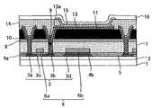
본 발명의 실시예 1에 따른 유기 EL표시장치에 대해, 도 1을 참조하여 설명한다. 도 1은, 본 실시예에 따른 유기 EL표시장치의 구성을 도시한 도면이다. 도 1에 나타내는 바와 같이, 본 실시예에 따른 유기 EL표시장치(100)는, 절연성 기판(1), 버퍼층(2), 다결정 실리콘 막(3), 제1 메탈막(4a, 4b), 게이트 절연막(5), 제2 메탈막(6), 층간 절연막(7), 패시베이션 막(8), 콘택홀(9), 제3 메탈막(10), 평탄화 막(11), 콘택홀(12), 애노드 전극(13), 분리막(14), 발광층(15), 캐소드 전극(16)을 갖고 있다.An organic EL display device according to
절연성 기판(1)은, 유리 기판이나 석영 기판 등의 투과성을 갖는 기판이다. 절연성 기판(1) 위에는, 버퍼층(2)이 형성되는 것이 바람직하다. 버퍼층(2)은, 절연성 기판(1)으로부터 유출하는 불순물로부터 후술하는 TFT를 보호하기 위해 설치 된다. 버퍼층(2)으로서는, SiN이나 SiO2 또는 그것들의 적층막을 사용할 수 있다.The
버퍼층(2)위에는, 반도체막인 다결정 실리콘 막(3)이 설치된다. 다결정 실리콘 막(3)은, 버퍼층(2) 위에 섬 모양으로 형성되어 있다. 다결정 실리콘 막(3)은, 소스 영역(3a), 드레인 영역(3b), 채널 영역(3c) 및 커패시터 전극(3d)이 되는 영역을 포함한다.On the
다결정 실리콘 막(3) 중, 소스 영역(3a), 드레인 영역(3b), 커패시터 전극(3d) 위에는, 도전 막이 접촉하도록 형성되어 있다. 구체적으로는, 소스 영역(3a) 및 드레인 영역(3b) 위에는, 도전 막인 제1 메탈막 4a가 형성되어 있다. 제1 메탈막 4a는, 후의 공정에서 형성되는 콘택홀(9)이 다결정 실리콘 막(3)의 소스 영역(3a), 드레인 영역(3b)이 관통하는 것을 방지하기 위해 설치된다. 즉, 제1 메탈막 4a는, 에칭 스토퍼의 역할을 한다. 또한 커패시터 전극(3d) 위에는, 도전 막인 제1 메탈막 4b가 형성되어 있다. 이와 같이, 커패시터 전극(3d) 위에 제1 메탈막 4b가 형성되어 있기 때문에, 다결정 실리콘 막으로 이루어지는 커패시터 전극(3d)에 불순물을 도입할 필요가 없다. 이 때문에, 커패시터 전극(3d)에 불순물의 주입을 행하기 위한 공정을 삭감할 수 있다. 또한, 제1 메탈막(4a, 4b)으로서는, Mo, Cr, W, Ti등을 사용할 수 있다.In the
제1 메탈막(4a, 4b) 위에는, 제1 메탈막(4a, 4b) 및 다결정 실리콘 막(3)을 덮도록, 게이트 절연막(5)이 형성되어 있다. 그리고, 게이트 절연막(5) 위에는, 제2 메탈막(6)이 형성되어 있다. 제2 메탈막(6)은, 게이트 전극(6a), 커패시터 전 극(6b)을 포함한다. 그리고, 제2 메탈막(6) 위에는, 층간 절연막(7)이 형성되어 있다. 또한 층간 절연막(7)위에는, 층간 절연막을 피복하도록 패시베이션 막(8)이 설치된다. 층간 절연막(7) 및 패시베이션 막(8)은, SiO2, SiN, SiON 중 어느 하나 또는 이들의 적층막으로 이루어진다.The
패시베이션 막(8), 층간 절연막(7), 게이트 절연막(6)에는, 이들의 막을 관통하여 설치된 콘택홀(9)이 설치된다. 콘택홀(9)은, 하층에 형성된 소스 영역(3a), 드레인 영역(3b)을 노출하도록 개구되어 있다. 패시베이션 막(8) 위에는, 제3 메탈막(10)이 설치된다. 제3 메탈막(10)으로서는, Al이나 Al을 주성분으로 하는 합금막, Mo, Cr, W, Ta이나 이들을 주성분으로 하는 합금막 또는 그것들의 적층구조를 사용할 수 있다. 제3 메탈막(10)은, 소스 전극, 드레인 전극을 포함하는 신호 배선이 된다. 즉, 패시베이션 막(8) 위에 설치된 신호 배선은, 패시베이션 막(8), 층간 절연막(7) 및 게이트 절연막(5)에 관통하여 설치된 콘택홀(9)을 통해, 반도체층인 다결정 실리콘 막(3)과 접속되어 있다. 이와 같이, 제3 메탈막(10)을 패시베이션 막(8) 위에 형성함으로써, 콘택홀(9)을 패시베이션 막(8), 층간 절연막(7), 게이트 절연막(6)을 관통하도록 일괄로 형성할 수 있다. 종래, 패시베이션 막의 스루홀과, 층간 절연막 및 게이트 절연막에 형성되는 콘택홀은, 별도의 공정으로 형성하고 있었다. 그러나, 본 발명에 의하면, 패시베이션 막(8), 층간 절연막(7) 및 게이트 절연막(5)을 관통하는 콘택홀(9)을 일괄로 형성할 수 있고, 제조 공정을 삭감할 수 있다.The
또한 제3 메탈막(10) 위에는, 패시베이션 막(8)을 피복하도록, 평탄화 막(11)이 설치된다. 그리고, 평탄화 막(11)에는, 하층의 제3 메탈막(10)을 노출시키는 콘택홀(12)이 형성되어 있다. 또한 평탄화 막(11)위에는, 이 평탄화 막(11)에 설치된 콘택홀(12)을 통해 신호 배선이 되는 제3 메탈막(10)과 접속된 애노드 전극(13)이 설치된다. 그리고, 애노드 전극(13) 위에는, 분리막(14)이 설치된다. 분리막(14)은, 후술하는 EL소자를 분리한다. 분리막(14)에는, 애노드 전극(13)을 노출하는 개구부가 설치된다.The
분리막(14)의 개구부에는, 애노드 전극(13)에 접촉하도록 발광층(15)이 설치된다. 발광층(15)은, 예를 들면 도시하지 않은 홀 수송층, 발광층, 전자 수송층, 전자 주입층 등의 복수의 층으로 구성된다. 발광층(15)은, 애노드 전극(13)과의 접촉부에 홀 수송층을 구비하고 있다. 애노드 전극(13)은, 이 홀 수송층보다도 일함수가 큰 재료가 이용되는 것이 바람직하다. 즉, 홀 수송층보다도 일함수가 큰 ITO나 IZO으로 이루어지는 투명도전 막이나, Pt, Au, Ir, Cr, Ag, Ni, Al 및 이들의 합금 등을 사용할 수 있다. 이에 따라 애노드 전극(13)과 홀 수송층과의 에너지 장벽을 저감시킬 수 있어, 발광 효율을 향상시키는 것이 가능하게 된다. 발광층(15) 위에는, 캐소드 전극(16)이 설치된다. 애노드 전극(13), 발광층(15), 캐소드 전극(16)이 적층 되어, EL소자가 형성된다. 유기 EL표시장치에는, 복수의 유기 EL소자가 매트릭스 모양으로 형성되어 있다.In the opening of the
다음에 상기의 액티브형 유기 EL표시장치의 제조 방법에 대해 도 2를 참조하여 설명한다. 도 2는, 본 실시예에 따른 유기 EL표시장치의 제조 방법을 설명하기 위한 도면이다. 도 2에 나타내는 바와 같이, 우선, 절연성 기판 위에 아모퍼스 실리콘의 바탕막으로서 SiN이나 SiO2 또는 그것들의 적층막으로 이루어지는 버퍼층(2)이 형성된다(스텝S1). 그리고, 버퍼층(2)위에, 다결정 실리콘 막(3)이 형성된다(스텝S2). 구체적으로는, 우선, 버퍼층(2)위에, 아모퍼스 실리콘 막이 형성된다. 아모퍼스 실리콘 막은, 플라즈마 CVD법에 의해, 두께 50∼70nm이 되도록 형성된다. 그 후에 엑시머레이저 어닐 혹은 YAG 레이저 어닐 등에 의해, 아모퍼스 실리콘 막을 용융, 냉각, 고화하여, 다결정 실리콘 막(3)을 얻을 수 있다. 그 후에 드라이 에칭에 의해 다결정 실리콘 막(3)을 섬 모양으로 가공한다(제1사진제판공정).Next, a method of manufacturing the above-described active organic EL display device will be described with reference to FIG. 2 is a diagram for explaining the manufacturing method of the organic EL display device according to the present embodiment. 2, the first, on an insulating substrate a film of amorphous silicon on the
다결정 실리콘 막(3)을 섬 모양으로 가공한 후, Mo, Cr, W, Ti등의 제1 메탈막(4a, 4b)이 형성된다(스텝S3). 그 후에 트랜지스터의 소스 영역(3a)/드레인 영역(3b)이 되는 개소 및 커패시터 전극(3d)이 되는 개소에, 제1 메탈막(4a, 4b)이 남도록 패터닝을 실시한다(제2사진제판공정).After the
또한, 상기에 있어서는, 다결정 실리콘 막(3)의 패터닝과, 콘택 메탈이 되는 제1메탈막(4a, 4b)의 패터닝을 별도의 사진제판공정으로 실시하고 있지만, 하프톤이나 그레이톤 마스크를 사용하여 1회의 사진제판공정으로 실시하는 것도 가능하다.In the above, the patterning of the
다결정 실리콘 막(3), 제1 메탈막(4a, 4b) 형성후, 절연성 기판(1) 전체면에 플라즈마 CVD법에 의해 게이트 절연막(5)이 형성된다(스텝S4). 그리고, 게이트 절연막(5)을 형성한 후, DC마그네트론을 사용한 스퍼터링법에 의해, 게이트 전 극(6a), 커패시터 전극(6b) 및 배선(도시하지 않음)을 형성하기 위한 제2 메탈막(6)이 성막된다(스텝S5). 제2 메탈막(6)으로서는, Mo, Cr, W, Al, Ta이나 이들을 주성분으로 하는 합금막을 사용할 수 있다. 그 후에 제2 메탈막(6)의 패터닝을 함으로써, 게이트 전극(6a), 커패시터 전극(6b) 및 배선을 얻을 수 있다(제3사진제판공정).After the
게이트 전극(6a), 커패시터 전극(6b), 배선을 패터닝한 후, 트랜지스터의 소스 영역(3a)/드레인 영역(3b)을 형성한다(스텝S6). 구체적으로는, 이온주입법 혹은 이온 도핑법으로, 제1 및 제2 불순물 도입을 행한다. 도입하는 불순물 원소로서는, P(인)이나 B(붕소)를 사용할 수 있다. 불순물로서 P을 도입하면 n형의 트랜지스터를 형성할 수 있고, B를 도입하면 p형의 트랜지스터를 형성할 수 있다. 또한 게이트 전극(6a)의 가공을 n형 트랜지스터용 게이트 전극과 p형 트랜지스터용 게이트 전극의 2회로 나누어 행하면, n형과 p형의 트랜지스터를 동일 기판 위에 나누어 만들 수 있다(제4사진제판공정).After the
또한 트랜지스터의 신뢰성 향상을 위해, 저농도 불순물 영역을 형성한 LDD구조로 하는 것도 가능하다. 저농도 불순물 영역의 형성 방법에는 몇 가지 방법이 있지만, 일반적인 형성 방법으로서는, 게이트 전극(6a)을 형성한 후, 이 게이트 전극(6a)을 마스크로서, 다결정 실리콘 막(3)에 저농도 불순물에 의해 제3 불순물 주입을 행한다. 다음에 게이트 전극(6a) 위에 이 게이트 전극(6a)으로부터 소정의 돌출을 갖는 상태의 레지스트 패턴을 사진제판에 의해 형성한다. 그 후에 제3 불순물 주입에 의해 불순물 농도가 높은 제1 불순물 주입을 행한다. 그리고, 제1 불순물 주입 완료후, 게이트 전극 위의 레지스트 패턴을 제거함으로써, 게이트 전극(6a)으로부터 튀어나온 레지스트 패턴 바로 아래에는 저농도 불순물 영역(LDD)이 형성된다. NMOS, PMOS 모두, LDD구조로 할 경우에는, 상기의 LDD형성 프로세스를 NMOS, PMOS각각에서 실시하면 된다(제5, 제6사진제판공정).In addition, in order to improve the reliability of the transistor, it is also possible to have an LDD structure in which a low concentration impurity region is formed. There are several methods for forming the low concentration impurity region. As a general formation method, after the
트랜지스터의 소스 영역(3a)/드레인 영역(3b)을 형성한 후, 플라즈마 CVD법에 의해, SiO2 혹은 SiN등의 층간 절연막(7)이 형성된다(스텝S7). 그 후에 앞의 공정에 있어서 도입한 불순물을 활성화시키기 위해, 400℃이상의 열처리를 행한다.After the
열처리를 행한 후, SiN등으로 이루어지는 패시베이션 막(8)이 형성된다(스텝S8). 패시베이션 막(8)을 형성한 후, 게이트 절연막(5), 층간 절연막(7) 및 패시베이션 막(8)을 관통하도록 일괄로 콘택홀(9)이 형성된다(제7사진제판공정). 그리고, 패시베이션 막(8) 위에 소스 전극, 드레인 전극 등의 신호 배선이 되는 제3 메탈막(10)이 형성된다(스텝S9). 이에 따라 콘택홀(9)을 통해, 패시베이션 막(8) 위에 형성된 소스 전극, 드레인 전극이 각각 다결정 실리콘 막(3)의 소스 영역(3a), 드레인 영역(3b)에 접속된다(제8사진제판공정). 소스 전극, 드레인 전극이 되는 제3 메탈막(10)은, DC마그네트론을 사용한 스퍼터링법에 의해 성막된다. 제3 메탈막(10)으로서는, Al이나 Al을 주성분으로 하는 합금막, Mo, Cr, W, Ta이나 이들을 주성분으로 하는 합금막 또는 그것들의 적층구조로 할 수 있다. 제3 메탈막의 가공은, 웨트 에칭, 드라이 에칭 어느 것이어도 된다.After the heat treatment, a
종래 기술에 있어서의 게이트 절연막, 층간 절연막에 형성된 콘택홀 및 이것 과는 다른 공정으로 형성된 패시베이션 막의 스루홀은, 본 실시예에 있어서는, 게이트 절연막, 층간 절연막 및 패시베이션 막에 동시에 형성되는 콘택홀이 된다.In the prior art, the through hole of the gate insulating film, the contact hole formed in the interlayer insulating film, and the passivation film formed by a process different from this are the contact holes formed simultaneously in the gate insulating film, the interlayer insulating film, and the passivation film. .
본 실시예에 있어서는, 다결정 실리콘 막(3)의 소스 영역(3a)/드레인 영역(3b)의 바로 위에는, 도전 막인 제1 메탈막 4a가 형성되어 있다. 이 때문에, 콘택홀(9)은, 트랜지스터의 소스/드레인 영역이 되는 다결정 실리콘 막(3) 바로 위의 제1 메탈막 4a 위에 형성된다. 종래, 다결정 실리콘 막의 바로 위에는 도전 막은 형성되지 않았다. 이 때문에, 콘택홀이 다결정 실리콘 막을 뚫고 나가는 경우가 있어, 프로세스 윈도우가 좁았다. 그러나, 본 발명에 의하면, 게이트 절연막(5)과 다결정 실리콘 막(3)의 바로 위에 형성한 제1 메탈막 4a와의 선택비를 높게 얻을 수 있다. 이 때문에, 콘택홀(9)의 형성 시, 다결정 실리콘 막(3)을 콘택홀(9)이 관통하는 것을 방지할 수 있다.In this embodiment, the
그리고, 제3 메탈막(10)을 형성한 후, TFT표면을 평탄화하기 위해, 감광성을 갖는 아크릴수지 혹은 폴리이미드 막으로 이루어지는 평탄화 막(11)이 형성된다(스텝S1O). 이 평탄화 막(11)은, 제3 메탈막(10)과 후술하는 애노드 전극(13)을 접속하기 위한 콘택홀(12)을 형성하기 위해 패터닝 된다(제9사진제판공정).After the
그 후에 평탄화 막(11) 위에 애노드 전극(13)이 되는 제4 메탈막을 형성한다(제10의 사진제판공정). 애노드 전극(13)은, 제3 메탈막(10) 위의 평탄화 막(11)을 개구한 콘택홀(12)을 통해 제3 메탈막(10)과 접속된다. 애노드 전극(13) 형성 후, EL소자를 분리하기 위한 분리막(14)이 형성되어, EL층(15), 캐소드 전극(16)의 형성이 행해진다.Thereafter, a fourth metal film to be the
이상에서 설명한 바와 같이, 본 발명의 실시예 1에 의하면, 액티브형 유기 EL표시장치의 애노드 전극(13)을 형성할 때까지의 구조를 9∼10회의 사진제판공정으로 형성할 수 있다. 이와 같이, 제조 공정수를 삭감할 수 있기 때문에, 유기 EL표시장치의 비용을 삭감하는 것이 가능하게 된다. 또한 다결정 실리콘 막(3)으로의 콘택홀(9)은, 다결정 실리콘 막(3)의 바로 위에 형성한 도전 막 위에 형성하면 되므로, 다결정 실리콘 막(3)을 관통하는 것을 방지할 수 있다. 이와 같이, 프로세스 윈도우를 넓게 할 수 있기 때문에, 제조 수율의 향상을 도모할 수 있다.As described above, according to the first embodiment of the present invention, the structure until the
실시예 2.Example 2.
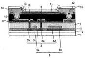
본 발명의 실시예 2에 대해, 도 3을 참조하여 설명한다. 도 3은, 본 실시예에 따른 유기 EL표시장치의 구성을 도시한 도면이다. 도 3에 있어서, 도 1과 동일한 구성요소에는 동일 부호를 붙여 설명을 생략한다.
도 3에 나타내는 바와 같이, 본 실시예에 있어서는, 실시예 1과 달리, 신호 배선이 되는 제3 메탈막(10)이 평탄화 막(11) 위에 형성된다. 즉, 평탄화 막(11)은, 제3 메탈막(10)과, 패시베이션 막(8) 사이에 설치된다. 제3 메탈막(10)과 다결정 실리콘 막(3)을 접속하기 위한 콘택홀(9)은, 게이트 절연막(5), 층간 절연막(7), 패시베이션 막(8), 평탄화 막(11)을 관통하여 설치된다. 또한 애노드 전극(13)과 제3 메탈막은, 평탄화 막(11) 위에 접속되어 있다. 또한, 제3 메탈막(10)의 단부는, 애노드 전극(13)이 되는 제4 메탈막으로 피복되고 있다. 즉, 애노드 전극(13)은, 제3 메탈막(10)의 윗면 및 측면에서 접속된다.As shown in FIG. 3, in the present embodiment, unlike the first embodiment, the
상기한 바와 같이, 실시예 1에 있어서는, 게이트 절연막(5), 층간 절연 막(7), 패시베이션 막(8)을 관통하는 콘택홀(9)을 형성한 후에, 신호 배선 등이 되는 제3 메탈막(10)을 형성하여 다결정 실리콘 막(3)과 접속했다. 그리고, 제3 메탈막(10)을 형성한 후에 평탄화 막(11)을 형성했다. 본 실시예에 있어서는, 평탄화 막(11)에 형성되는 콘택홀의 형성시에, 패시베이션 막(8), 층간 절연막(7), 게이트 절연막(5)의 콘택홀도 동시에 형성한다. 이에 따라 사진제판공정을 1회 삭감하는 것이 가능하게 된다. 그리고, 평탄화 막(11)을 형성한 후에, 제3 메탈막(10)이 형성된다. 그 후에 제3 메탈막(10)의 단부를 덮도록 애노드 전극(13)이 되는 제4 메탈막을 형성함으로써, 제3 메탈막(10)과 애노드 전극(13)을 접속할 수 있다.As described above, in Example 1, after forming the
실시예 3.Example 3.
본 발명의 실시예 3에 따른 유기 EL표시장치에 대해, 도 4를 참조하여 설명한다. 도 4는, 본 발명의 실시예에 따른 유기 EL표시장치의 구성을 나타내는 도면이다. 또한, 도 4에 있어서는, 도 1과 동일한 구성요소에는 동일 부호를 붙여 설명을 생략한다.An organic EL display device according to
실시예 2에 있어서는, 신호 배선이 되는 제3 메탈막(10)과 애노드 전극(13)은 다른 재료로 형성되어, 각각을 평탄화 막(11) 위에서 접속하는 구조로 했다. 본 실시예에 있어서는, 애노드 전극(13)은 제3 메탈막(10)과 같은 재료로 형성되어, 제3 메탈막(10)으로부터 연장하고 있다. 즉, 애노드 전극(13)과 제3 메탈막(10)은, 동일한 공정으로 형성된다. 이에 따라 사진제판공정을 또한 1회 삭감할 수 있다.In Example 2, the
실시예 4.Example 4.
본 발명의 실시예 4에 따른 유기 EL표시장치에 대해, 도 5를 참조하여 설명 한다. 도 5는, 본 실시예에 따른 유기 EL표시장치의 구성을 도시한 도면이다. 도 5에 있어서, 도 1과 동일한 구성요소에는 동일한 부호를 붙여, 설명을 생략한다.An organic EL display device according to Embodiment 4 of the present invention will be described with reference to FIG. 5 is a diagram showing the configuration of the organic EL display device according to the present embodiment. In FIG. 5, the same code | symbol is attached | subjected to the component same as FIG. 1, and description is abbreviate | omitted.
도 5에 나타내는 바와 같이, 실시예 3과 마찬가지로, 제3 메탈막(10)은 발광층(15) 아래까지 뻗어 있다. 애노드 전극(13)을 구성하는 제3 메탈막(10) 위에는, 콘택 메탈막(13a)이 설치된다. 따라서, 애노드 전극(13)은, 제3 메탈막(10)과 콘택 메탈막(13a)이 적층된 구조를 갖는다. 콘택 메탈막(13a)으로서는, ITO 혹은 IZO등, 홀 수송층보다도 일함수가 큰 재료를 사용할 수 있다. 이에 따라 애노드 전극(13)과 홀 수송층과의 에너지 장벽을 저감시킬 수 있고, 발광 효율을 향상시키는 것이 가능하게 된다.As shown in FIG. 5, similar to the third embodiment, the
또한, ITO 혹은 IZO등의 콘택 메탈막(13a)은 도 5에 나타내는 바와 같이 발광층(15) 아래에만 있어도 되고, 또는, 도 6에 나타내는 바와 같이 제3 메탈막(10)의 전체면에 걸쳐 형성해도 좋다.In addition, the
이상에서 설명한 바와 같이, 본 발명에 의하면, 제조 공정수를 삭감할 수 있으므로, 비용의 삭감을 실현하는 것이 가능하게 된다. 또한 커패시터 전극(3b) 위에 도전 막을 형성함으로써, 불순물 도입 공정을 삭감할 수 있다. 또한 다결정 실리콘 막(3)으로의 콘택홀(9)은, 다결정 실리콘 막(3)의 바로 위에 형성한 도전 막 위에 형성하면 되므로, 다결정 실리콘 막(3)을 관통하는 것을 방지할 수 있다.As described above, according to the present invention, since the number of manufacturing steps can be reduced, the cost can be reduced. In addition, the impurity introduction step can be reduced by forming a conductive film on the
또한, 상기의 실시예에 있어서는, 유기 EL표시장치의 표시 영역에 설치된 TFT에 대하여 설명했지만, 이것에 한정되는 것은 아니다. 예를 들면 표시 영역 이외에도, 주변부에 설치되는 구동회로의 TFT에 적용하는 것도 가능하다. 또한 다른 톱 게이트형의 TFT를 이용한 표시장치에 있어서도 적용할 수 있다.In the above embodiment, the TFT provided in the display area of the organic EL display device has been described, but the present invention is not limited thereto. For example, it is also possible to apply to TFT of the drive circuit provided in a peripheral part besides a display area. The present invention can also be applied to display devices using other top gate type TFTs.
도 1은 실시예 1에 따른 유기 EL표시장치의 구성을 나타내는 도면이다.1 is a diagram showing the configuration of an organic EL display device according to a first embodiment.
도 2는 실시예 1에 따른 유기 EL표시장치의 제조 방법을 설명하기 위한 플로우도이다.2 is a flowchart for explaining a method of manufacturing an organic EL display device according to the first embodiment.
도 3은 실시예 2에 따른 유기 EL표시장치의 구성을 나타내는 도면이다.3 is a diagram showing the configuration of an organic EL display device according to a second embodiment.
도 4는 실시예 3에 따른 유기 EL표시장치의 구성을 나타내는 도면이다.4 is a diagram showing the configuration of an organic EL display device according to a third embodiment.
도 5는 실시예 4에 따른 유기 EL표시장치의 구성을 나타내는 도면이다.5 is a diagram showing the configuration of an organic EL display device according to a fourth embodiment.
도 6은 실시예 4에 따른 유기 EL표시장치의 다른 구성을 나타내는 도면이다.6 is a diagram showing another configuration of the organic EL display device according to the fourth embodiment.
도 7은 종래의 유기 EL표시장치의 구성을 나타내는 도면이다.7 is a diagram showing the configuration of a conventional organic EL display device.
[부호의 설명][Description of the code]
1 : 절연성 기판 2 : 버퍼층1
3 : 다결정 실리콘 막 3a : 소스 영역3:
3b : 드레인 영역 3c : 채널 영역3b: drain
3d : 커패시터 전극 4a, 4b : 제1 메탈막3d:
5 : 게이트 절연층 6 : 제2 메탈층5
6a : 게이트 전극 6b : 커패시터 전극6a:
7 : 층간 절연막 8 : 패시베이션 막7 interlayer insulating
9 : 콘택홀 10 : 제3 메탈층9: contact hole 10: third metal layer
11 : 평탄화 막 12 : 콘택홀11: planarization film 12: contact hole
13 : 애노드 전극 13a : 콘택 메탈막13
14 : 분리막 15 : 발광층14
16 : 캐소드 전극16: cathode electrode
Claims (20)
Translated fromKoreanApplications Claiming Priority (2)
| Application Number | Priority Date | Filing Date | Title |
|---|---|---|---|
| JP2007171501AJP2009010242A (en) | 2007-06-29 | 2007-06-29 | Display device and manufacturing method thereof |
| JPJP-P-2007-00171501 | 2007-06-29 |
Publications (1)
| Publication Number | Publication Date |
|---|---|
| KR20090004500Atrue KR20090004500A (en) | 2009-01-12 |
Family
ID=40325021
Family Applications (1)
| Application Number | Title | Priority Date | Filing Date |
|---|---|---|---|
| KR1020080053012ACeasedKR20090004500A (en) | 2007-06-29 | 2008-06-05 | Display device and manufacturing method thereof |
Country Status (2)
| Country | Link |
|---|---|
| JP (1) | JP2009010242A (en) |
| KR (1) | KR20090004500A (en) |
Cited By (2)
| Publication number | Priority date | Publication date | Assignee | Title |
|---|---|---|---|---|
| US11626471B2 (en) | 2020-09-14 | 2023-04-11 | Samsung Display Co., Ltd. | Display device including transistor with separate insulating patterns and etch stoppers overlying active layer thereof, and method of manufacturing the same |
| US11751439B2 (en) | 2020-07-07 | 2023-09-05 | Samsung Display Co., Ltd. | Display device and manufacturing method thereof including contact holes optimized to prevent excess hydrogen from introducing into semiconductor layer |
Family Cites Families (4)
| Publication number | Priority date | Publication date | Assignee | Title |
|---|---|---|---|---|
| JP4772228B2 (en)* | 2000-07-31 | 2011-09-14 | 株式会社半導体エネルギー研究所 | Method for manufacturing light emitting device |
| JP2005285977A (en)* | 2004-03-29 | 2005-10-13 | Seiko Epson Corp | Semiconductor device, electro-optical device and electronic apparatus |
| KR100712295B1 (en)* | 2005-06-22 | 2007-04-27 | 삼성에스디아이 주식회사 | Organic electroluminescent device and manufacturing method thereof |
| JP2007173652A (en)* | 2005-12-23 | 2007-07-05 | Mitsubishi Electric Corp | THIN FILM TRANSISTOR DEVICE, MANUFACTURING METHOD THEREOF, AND DISPLAY DEVICE HAVING THE THIN FILM TRANSISTOR DEVICE |
- 2007
- 2007-06-29JPJP2007171501Apatent/JP2009010242A/enactivePending
- 2008
- 2008-06-05KRKR1020080053012Apatent/KR20090004500A/ennot_activeCeased
Cited By (3)
| Publication number | Priority date | Publication date | Assignee | Title |
|---|---|---|---|---|
| US11751439B2 (en) | 2020-07-07 | 2023-09-05 | Samsung Display Co., Ltd. | Display device and manufacturing method thereof including contact holes optimized to prevent excess hydrogen from introducing into semiconductor layer |
| US11626471B2 (en) | 2020-09-14 | 2023-04-11 | Samsung Display Co., Ltd. | Display device including transistor with separate insulating patterns and etch stoppers overlying active layer thereof, and method of manufacturing the same |
| US11917878B2 (en) | 2020-09-14 | 2024-02-27 | Samsung Display Co., Ltd. | Display device including transistor with vias contacting active layer through etch stop layer, and method of manufacturing same |
Also Published As
| Publication number | Publication date |
|---|---|
| JP2009010242A (en) | 2009-01-15 |
Similar Documents
| Publication | Publication Date | Title |
|---|---|---|
| JP4309362B2 (en) | Thin film transistor manufacturing method | |
| KR100307456B1 (en) | Method for manufacturing Thin Film Transistor | |
| JP4404881B2 (en) | Thin film transistor array, manufacturing method thereof, and liquid crystal display device | |
| US6617203B2 (en) | Flat panel display device and method of manufacturing the same | |
| EP2985784B1 (en) | Low-temperature poly-silicon tft array substrate, manufacturing method therefor, and display apparatus | |
| KR101415684B1 (en) | Substrate for organic electro luminescent device and method of fabricating the same | |
| JP4690187B2 (en) | Organic light emitting display device and method for manufacturing the same | |
| KR100501867B1 (en) | Top gate type thin film transistor | |
| US10468533B2 (en) | Semiconductor device and method for manufacturing same | |
| US6995048B2 (en) | Thin film transistor and active matrix type display unit production methods therefor | |
| KR101021479B1 (en) | A thin film transistor, a method of forming the same, and a flat panel display including the thin film transistor | |
| WO2015194417A1 (en) | Semiconductor device | |
| CN103155019B (en) | Thin film transistor array device, EL display panel, EL display device, manufacturing method of thin film transistor array device, and manufacturing method of EL display panel | |
| KR20180137641A (en) | Display device and method of manufacturing the same | |
| WO2019186924A1 (en) | Display device and production method for display device | |
| KR101026808B1 (en) | Method of manufacturing thin film transistor array panel | |
| KR100811997B1 (en) | Thin film transistor and its manufacturing method and flat panel display device including the same | |
| KR100590249B1 (en) | Organic light emitting display device and manufacturing method thereof | |
| JP2010108957A (en) | Display device and method of manufacturing the same | |
| JP4633434B2 (en) | Semiconductor device and manufacturing method thereof | |
| KR20190076094A (en) | Display device and method for manufacturing the same | |
| US20050112807A1 (en) | Thin film transistor, method of fabricating the same and flat panel display using thin film transistor | |
| KR20090004500A (en) | Display device and manufacturing method thereof | |
| JP2001100663A (en) | EL display device | |
| US7235850B2 (en) | Thin film transistor, method of fabricating the same, and flat panel display using thin film transistor |
Legal Events
| Date | Code | Title | Description |
|---|---|---|---|
| A201 | Request for examination | ||
| PA0109 | Patent application | Patent event code:PA01091R01D Comment text:Patent Application Patent event date:20080605 | |
| PA0201 | Request for examination | ||
| PG1501 | Laying open of application | ||
| E902 | Notification of reason for refusal | ||
| PE0902 | Notice of grounds for rejection | Comment text:Notification of reason for refusal Patent event date:20091030 Patent event code:PE09021S01D | |
| E601 | Decision to refuse application | ||
| PE0601 | Decision on rejection of patent | Patent event date:20100127 Comment text:Decision to Refuse Application Patent event code:PE06012S01D Patent event date:20091030 Comment text:Notification of reason for refusal Patent event code:PE06011S01I |