KR20090003854A - Image sensor and its manufacturing method - Google Patents
Image sensor and its manufacturing methodDownload PDFInfo
- Publication number
- KR20090003854A KR20090003854AKR1020070067575AKR20070067575AKR20090003854AKR 20090003854 AKR20090003854 AKR 20090003854AKR 1020070067575 AKR1020070067575 AKR 1020070067575AKR 20070067575 AKR20070067575 AKR 20070067575AKR 20090003854 AKR20090003854 AKR 20090003854A
- Authority
- KR
- South Korea
- Prior art keywords
- region
- gate
- substrate
- forming
- transfer gate
- Prior art date
- Legal status (The legal status is an assumption and is not a legal conclusion. Google has not performed a legal analysis and makes no representation as to the accuracy of the status listed.)
- Withdrawn
Links
Images


Classifications
- H—ELECTRICITY
- H10—SEMICONDUCTOR DEVICES; ELECTRIC SOLID-STATE DEVICES NOT OTHERWISE PROVIDED FOR
- H10F—INORGANIC SEMICONDUCTOR DEVICES SENSITIVE TO INFRARED RADIATION, LIGHT, ELECTROMAGNETIC RADIATION OF SHORTER WAVELENGTH OR CORPUSCULAR RADIATION
- H10F39/00—Integrated devices, or assemblies of multiple devices, comprising at least one element covered by group H10F30/00, e.g. radiation detectors comprising photodiode arrays
- H10F39/10—Integrated devices
- H10F39/12—Image sensors
- H—ELECTRICITY
- H10—SEMICONDUCTOR DEVICES; ELECTRIC SOLID-STATE DEVICES NOT OTHERWISE PROVIDED FOR
- H10F—INORGANIC SEMICONDUCTOR DEVICES SENSITIVE TO INFRARED RADIATION, LIGHT, ELECTROMAGNETIC RADIATION OF SHORTER WAVELENGTH OR CORPUSCULAR RADIATION
- H10F39/00—Integrated devices, or assemblies of multiple devices, comprising at least one element covered by group H10F30/00, e.g. radiation detectors comprising photodiode arrays
- H10F39/80—Constructional details of image sensors
- H10F39/802—Geometry or disposition of elements in pixels, e.g. address-lines or gate electrodes
- H—ELECTRICITY
- H10—SEMICONDUCTOR DEVICES; ELECTRIC SOLID-STATE DEVICES NOT OTHERWISE PROVIDED FOR
- H10F—INORGANIC SEMICONDUCTOR DEVICES SENSITIVE TO INFRARED RADIATION, LIGHT, ELECTROMAGNETIC RADIATION OF SHORTER WAVELENGTH OR CORPUSCULAR RADIATION
- H10F39/00—Integrated devices, or assemblies of multiple devices, comprising at least one element covered by group H10F30/00, e.g. radiation detectors comprising photodiode arrays
- H10F39/011—Manufacture or treatment of image sensors covered by group H10F39/12
- H10F39/014—Manufacture or treatment of image sensors covered by group H10F39/12 of CMOS image sensors
- H—ELECTRICITY
- H10—SEMICONDUCTOR DEVICES; ELECTRIC SOLID-STATE DEVICES NOT OTHERWISE PROVIDED FOR
- H10F—INORGANIC SEMICONDUCTOR DEVICES SENSITIVE TO INFRARED RADIATION, LIGHT, ELECTROMAGNETIC RADIATION OF SHORTER WAVELENGTH OR CORPUSCULAR RADIATION
- H10F39/00—Integrated devices, or assemblies of multiple devices, comprising at least one element covered by group H10F30/00, e.g. radiation detectors comprising photodiode arrays
- H10F39/80—Constructional details of image sensors
- H10F39/803—Pixels having integrated switching, control, storage or amplification elements
Landscapes
- Solid State Image Pick-Up Elements (AREA)
Abstract
Translated fromKoreanDescription
Translated fromKorean본 발명은 이미지 센서 및 그 제조 방법에 관한 것으로서, 더욱 상세하게는 화질을 개선할 수 있는 이미지 센서 및 그 제조 방법에 관한 것이다.The present invention relates to an image sensor and a method of manufacturing the same, and more particularly, to an image sensor and a method of manufacturing the same that can improve the image quality.
일반적으로 이미지 센서(image sensor)란, 광학적 이미지를 전기적 신호로 변환시키는 반도체 소자이다. 이러한 이미지 센서는 크게 전하 결합 소자(CCD: Charge Coupled Device)와 CMOS 이미지 센서로 구분할 수 있다.In general, an image sensor is a semiconductor device that converts an optical image into an electrical signal. Such image sensors can be roughly classified into charge coupled devices (CCDs) and CMOS image sensors.
여기서, 전하 결합 소자란, 개개의 모스 캐패시터(MOS Capacitor)가 서로 매우 근접한 위치에 있으면서 전하 캐리어가 캐패시터에 저장되고 이송되는 소자이다. 그리고, CMOS 이미지 센서란, 제어 회로 및 신호처리 회로를 주변 회로로 사용하는 CMOS 기술을 이용하여 화소수만큼 모스 트랜지스터(MOS Transistor)를 만들고 이것을 이용하여 차례 차례로 출력을 검출하는 스위칭(Switching) 방식을 이용하는 소자이다.Here, the charge coupling device is a device in which charge carriers are stored and transported in a capacitor while the respective MOS capacitors are in close proximity to each other. In addition, a CMOS image sensor is a switching method in which a MOS transistor is formed by the number of pixels using CMOS technology using a control circuit and a signal processing circuit as peripheral circuits, and the output is sequentially detected using the CMOS image sensor. It is an element to use.
이 중, CMOS 이미지 센서는 일반적으로 빛을 감지하여 전기 신호를 발생시키는 액티브 픽셀 센서(APS: Active Pixel Sensor) 어레이 영역과, APS 어레이 영역 에서 발생된 전기 신호를 처리하는 로직 영역(주변 회로 영역)으로 구분될 수 있다.Among these, the CMOS image sensor generally includes an active pixel sensor (APS) array region that detects light and generates an electrical signal, and a logic region (a peripheral circuit region) that processes an electrical signal generated in the APS array region. It can be divided into.
그리고, APS 어레이 영역의 각 단위 픽셀들은 트랜스퍼 게이트 전극과, 트랜스퍼 게이트 전극 양측에 위치하는 포토 다이오드(photo diode) 및 플로팅 확산(floating diffusion) 영역을 포함한다.Each of the unit pixels of the APS array region includes a transfer gate electrode, a photo diode and a floating diffusion region positioned at both sides of the transfer gate electrode.
액티브 픽셀 센서의 동작에 대해 간단히 설명하면, 포토 다이오드에서 빛을 감지하면 전자-홀 쌍(EHP: electron-hole pair)이 생성되어 축적되며, 축적된 전자-홀 쌍은 트랜스퍼 트랜지스터의 동작에 의해 플로팅 확산 영역으로 전달된다. 이에 따라 플로팅 확산 영역에서의 전위가 변화하게 되며, 이러한 전위 변화를 감지하여 출력한다.Briefly describing the operation of an active pixel sensor, when light is detected by a photodiode, an electron-hole pair (EHP) is generated and accumulated, and the accumulated electron-hole pair is floated by the operation of the transfer transistor. Delivered to the diffusion region. As a result, the potential in the floating diffusion region changes, and the change in potential is detected and output.
그런데, 외부에서 빛이 포토 다이오드뿐만 아니라, 트랜스퍼 게이트의 상부로도 입사될 수 있다. 이러한 경우, 트랜스퍼 게이트로 입사된 빛은 트랜스퍼 게이트 하부의 채널 및/또는 플로팅 확산 영역에서도 전자-홀 쌍을 발생시킬 수 있으며, 포토 다이오드 이외의 영역에서 발생된 전자-홀 쌍들은 이미지 센서의 화질을 저하시킬 수 있다.However, light from outside may be incident not only to the photodiode but also to the upper portion of the transfer gate. In this case, light incident on the transfer gate may generate electron-hole pairs in the channel and / or floating diffusion region under the transfer gate, and electron-hole pairs generated in regions other than the photodiode may reduce the image quality of the image sensor. Can be reduced.
본 발명이 이루고자 하는 기술적 과제는 트랜스퍼 게이트로 빛이 입사되는 것을 차단할 수 있는 이미지 센서에 관한 것이다.The technical problem to be achieved by the present invention relates to an image sensor that can block the incident light to the transfer gate.
또한, 본 발명이 이루고자 하는 다른 기술적 과제는 이러한 이미지 센서의 제조 방법을 제공하는데 있다.In addition, another technical problem to be achieved by the present invention is to provide a method of manufacturing such an image sensor.
본 발명이 이루고자 하는 기술적 과제는 이상에서 언급한 과제에 제한되지 않으며, 언급되지 않은 또 다른 과제들은 아래의 기재로부터 당업자에게 명확하게 이해될 수 있을 것이다.The technical problem to be achieved by the present invention is not limited to the above-mentioned problem, and other problems not mentioned will be clearly understood by those skilled in the art from the following description.
상기 기술적 과제를 달성하기 위하여 본 발명의 일 실시예에 따른 이미지 센서는 픽셀 영역 및 로직 영역이 정의된 기판, 픽셀 영역의 기판 내에 형성되어 광전하를 축적하는 포토다이오드, 픽셀 영역의 기판 내에 형성되어 포토다이오드에 축적된 광전하를 전달받아 검출하는 플로팅 확산 영역, 픽셀 영역의 기판 상에 위치하여, 포토다이오드에 축적된 광전하를 플로팅 확산 영역으로 전달하는 트랜스퍼 게이트, 픽셀 영역의 기판 상에 위치하며, 플로팅 확산 영역을 주기적으로 리셋 시키는 리셋 소자, 픽셀 영역의 기판 상에 위치하며, 플로팅 확산 영역에 축적된 광전하를 증폭하는 드라이브 소자, 픽셀 영역의 기판 상에 위치하며, 단위 픽셀을 선택하는 선택 소자, 로직 영역의 기판에 형성되어 픽셀 영역에서 출력되는 신호를 처리하는 로직 소자들 및 트랜스퍼 게이트 및 로직 소자들의 상면에 형성된 실리사 이드막을 포함한다.In order to achieve the above technical problem, an image sensor according to an embodiment of the present invention is formed in a substrate in which a pixel region and a logic region are defined, a photodiode which is formed in a substrate of a pixel region and accumulates photocharges, and is formed in a substrate of a pixel region. A floating diffusion region that receives and detects photocharges accumulated in the photodiode, and a transfer gate that transfers the photocharges accumulated in the photodiode to the floating diffusion region and a substrate in the pixel region. A reset element for periodically resetting the floating diffusion region, a drive element positioned on the substrate of the pixel region, and a drive element amplifying the photocharges accumulated in the floating diffusion region, selected on the substrate of the pixel region, to select a unit pixel Elements, logic elements formed on the substrate of the logic region to process signals output from the pixel region And a silicide film formed on upper surfaces of the transfer gate and the logic elements.
상기 기술적 과제를 달성하기 위하여 본 발명의 다른 실시예에 따른 이미지 센서의 제조 방법은 픽셀 영역 및 로직 영역이 정의된 기판을 제공하고, 픽셀 영역의 기판 상에 트랜스퍼 게이트를, 로직 영역의 기판 상에 로직 소자들의 게이트를 형성하고, 트랜스퍼 게이트 일측의 기판 내에 포토다이오드를 형성하고, 트랜스퍼 게이트 타측의 기판 내에 플로팅 확산 영역을, 로직 영역의 게이트 양측의 기판 내에 불순물 영역을 형성하고, 픽셀 영역의 트랜스퍼 게이트 상면과, 로직 영역의 게이트 및 불순물 영역 상면에 실리사이드막을 형성하는 것을 포함한다.In order to achieve the above technical problem, a method of manufacturing an image sensor according to another embodiment of the present invention provides a substrate in which a pixel region and a logic region are defined, and a transfer gate is formed on a substrate in a pixel region and a substrate in a logic region. Forming a gate of logic elements, a photodiode in a substrate on one side of the transfer gate, a floating diffusion region in the substrate on the other side of the transfer gate, an impurity region in the substrate on both sides of the gate of the logic region, and a transfer gate in the pixel region. And forming a silicide film on the upper surface and the upper surface of the gate and the impurity region of the logic region.
기타 실시예들의 구체적인 사항들은 상세한 설명 및 도면들에 포함되어 있다.Specific details of other embodiments are included in the detailed description and the drawings.
본 발명의 이미지 센서 및 그 제조 방법에 따르면, 단위 픽셀 영역에서의 트랜스퍼 게이트 상면에 실리사이드막을 형성함으로써, 외부로부터 트랜스퍼 게이트로 빛이 입사되는 것을 차단할 수 있다. 그러므로, 수광 소자 이외의 영역에서 EHP가 발생하여 이미지 센서의 화질이 저하되는 것을 방지할 수 있다.According to the image sensor of the present invention and a method of manufacturing the same, by forming a silicide film on the upper surface of the transfer gate in the unit pixel region, it is possible to block the light from entering from the outside to the transfer gate. Therefore, it is possible to prevent the EHP from occurring in regions other than the light receiving element so that the image quality of the image sensor is deteriorated.
그리고, 단위 픽셀 영역의 트랜스퍼 게이트 상면과 로직 영역을 함께 노출시키는 절연막 패턴을 이용함으로써, 트랜스퍼 게이트 상면과 로직 영역 상에 실리사이드막을 동시에 형성할 수 있으므로, 이미지 센서의 제조 공정을 단순화할 수 있다.The silicide layer may be simultaneously formed on the upper surface of the transfer gate and the logic region by using an insulating layer pattern that exposes the upper portion of the transfer gate and the logic region of the unit pixel region, thereby simplifying the manufacturing process of the image sensor.
또한, 단위 픽셀 영역에서 트랜스퍼 게이트 상면만을 노출시키는 절연막 패 턴을 이용함으로써, 실리사이드화 공정시 단위 픽셀 영역이 금속 물질에 의한 영향으로 감도가 저하되는 것을 방지할 수 있다.In addition, by using an insulating layer pattern exposing only the upper surface of the transfer gate in the unit pixel region, the sensitivity of the unit pixel region may be prevented from being degraded due to the influence of the metal material during the silicide process.
본 발명의 이점 및 특징, 그리고 그것들을 달성하는 방법은 첨부되는 도면과 함께 상세하게 후술되어 있는 실시예를 참조하면 명확해질 것이다. 그러나 본 발명은 이하에서 개시되는 실시예에 한정되는 것이 아니라 서로 다른 다양한 형태로 구현될 수 있으며, 단지 본 실시예는 본 발명의 개시가 완전하도록 하고, 본 발명이 속하는 기술분야에서 통상의 지식을 가진 자에게 발명의 범주를 완전하게 알려주기 위해 제공되는 것이며, 본 발명은 청구항의 범주에 의해 정의될 뿐이다. 명세서 전문에 걸쳐 동일 참조 부호는 동일 구성 요소를 지칭한다.Advantages and features of the present invention, and methods for achieving them will be apparent with reference to the embodiments described below in detail in conjunction with the accompanying drawings. However, the present invention is not limited to the embodiments disclosed below, but may be implemented in various forms. It is provided to fully convey the scope of the invention to those skilled in the art, and the invention is defined only by the scope of the claims. Like reference numerals refer to like elements throughout the specification.
본 명세서에서 사용된 용어는 실시예들을 설명하기 위한 것이며 본 발명을 제한하고자 하는 것은 아니다. 본 명세서에서, 단수형은 문구에서 특별히 언급하지 않는 한 복수형도 포함한다. 명세서에서 사용되는 포함한다(comprises) 및/또는 포함하는(comprising)은 언급된 구성요소, 단계, 동작 및/또는 소자는 하나 이상의 다른 구성요소, 단계, 동작 및/또는 소자의 존재 또는 추가를 배제하지 않는다.The terminology used herein is for the purpose of describing particular embodiments only and is not intended to be limiting of the invention. In this specification, the singular also includes the plural unless specifically stated otherwise in the phrase. As used herein, including and / or comprising the components, steps, operations and / or elements mentioned exclude the presence or addition of one or more other components, steps, operations and / or elements. I never do that.
이하 본 발명의 실시예들에서는 이미지 센서의 일 예로 CMOS 이미지 센서를 예시할 것이다. 먼저, 도 1 내지 도 5를 참조하여 본 발명의 일 실시예에 따른 CMOS 이미지 센서의 구조에 대해 상세히 설명하기로 한다.Hereinafter, embodiments of the present invention will exemplify a CMOS image sensor as an example of an image sensor. First, a structure of a CMOS image sensor according to an exemplary embodiment of the present invention will be described in detail with reference to FIGS. 1 to 5.
도 1은 본 발명의 일 실시예에 따른 이미지 센서의 개략적인 블록도이다.1 is a schematic block diagram of an image sensor according to an embodiment of the present invention.
도 1을 참조하면, 이미지 센서는 수광 소자를 포함하는 픽셀들이 이차원적으 로 배열되어 이루어진 액티브 픽셀 센서(APS) 어레이 영역(10)과, APS 어레이 영역(10)을 동작시키기 위한 로직(logic) 영역(20)을 포함한다.Referring to FIG. 1, an image sensor includes an active pixel sensor (APS)
APS 어레이 영역(10)은 2차원적으로 배열된 복수의 픽셀을 포함하며, 광 신호를 전기적 신호로 변환한다. 이러한 APS 어레이 영역(10)은 행 드라이버(50)로부터 픽셀 선택 신호(SEL), 리셋 신호(RX), 전하 전송 신호(TX) 등 다수의 구동 신호를 수신하여 구동된다. 또한, 변환된 전기적 신호는 수직 신호 라인를 통해서 상관 이중 샘플러(50)에 제공된다.The
로직 영역(20)은 타이밍 발생기(timing generator; 30), 행 디코더(row decoder; 40), 행 드라이버(row driver; 50), 상관 이중 샘플러(CDS: Correlated Double Sampler; 60), 아날로그 디지털 컨버터(ADC: Analog to Digital Converter; 70), 래치부(latch; 80), 열 디코더(column decoder; 90) 등을 포함할 수 있다.The
타이밍 발생기(30)는 행 디코더(40) 및 열 디코더(90)에 타이밍(timing) 신호 및 제어 신호를 제공한다.The
행 드라이버(50)는 행 디코더(40)에서 디코딩된 결과에 따라 다수의 단위 픽셀들을 구동하기 위한 다수의 구동 신호를 APS 어레이 영역(10)으로 제공한다. 일반적으로 행렬 형태로 단위 픽셀이 배열된 경우에는 각 행별로 구동 신호를 제공한다.The
상관 이중 샘플러(60)는 APS 어레이 영역(10)에 형성된 전기 신호를 수직 신호 라인을 통해 수신하여 유지(hold) 및 샘플링한다. 즉, 특정한 잡음 레벨(noise level)과 형성된 전기적 신호에 의한 신호 레벨을 이중으로 샘플링하여, 잡음 레벨 과 신호 레벨의 차이에 해당하는 차이 레벨을 출력한다.The correlated
아날로그 디지털 컨버터(70)는 차이 레벨에 해당하는 아날로그 신호를 디지털 신호로 변환하여 출력한다.The analog-to-
래치부(80)는 디지털 신호를 래치(latch)하고, 래치된 신호는 열 디코더(90)에서 디코딩 결과에 따라 순차적으로 영상 신호 처리부(도면 미도시)로 출력된다.The
도 2는 본 발명의 실시예들에 따른 이미지 센서의 액티브 픽셀 센서(APS) 어레이의 간략 회로도이다.2 is a simplified circuit diagram of an active pixel sensor (APS) array of image sensors in accordance with embodiments of the present invention.
도 2를 참조하면, 이미지 센서에서 광 신호를 전기적인 신호로 변환하는 APS 어레이 영역(10)은 도 3에 도시된 등가 회로도로 구성된 단위 픽셀(100)들이 매트릭스 형태로 배열되어 구성된다.Referring to FIG. 2, the
도 3은 본 발명의 실시예들에 따른 이미지 센서의 단위 픽셀의 회로도이다.3 is a circuit diagram of a unit pixel of an image sensor according to example embodiments.
도 3에서는 단위 픽셀 영역(100)이 4개의 트랜지스터 구조로 이루어진 경우를 도시하고 있으나, 단위 픽셀 영역(100)은 3개의 트랜지스터 구조, 5개의 트랜지스터 구조 또는 4개의 트랜지스터 구조와 유사한 포토게이트 구조로 구성될 수도 있다.In FIG. 3, the
도 3을 참조하면, 4개의 트랜지스터 구조로 이루어진 각 단위 픽셀 영역(100)은 빛을 받아 광전하를 생성 및 축적하는 수광 소자(110)와, 수광 소자에 입사된 광 신호를 독출하는 독출 소자로 구분될 수 있다. 독출 소자로는 리셋(reset) 소자(140), 드라이브(drive) 소자(150), 선택(select) 소자(160) 등이 포함될 수 있다.Referring to FIG. 3, each
보다 상세히 설명하면, 수광 소자(110)는 입사광에 대응하는 전하를 생성 및 축적하며, 수광 소자로는 포토 다이오드(photo diode), 포토 트랜지스터(photo transistor), 포토 게이트(photo gate), 핀드 포토 다이오드(Pinned Photo Diode; PPD) 및 이들의 조합이 가능하다. 그리고 수광 소자(110)는 축적된 광전하를 플로팅 확산 영역(120, FD; Floating Diffusion region)으로 전달하는 전하 전송 소자(130)와 연결된다.In more detail, the
플로팅 확산 영역(120)은 수광 소자(110)에서 축적된 전하를 전송받는다. 그리고 플로팅 확산 영역(120)은 기생 커패시턴스를 갖고 있기 때문에, 전하가 누적적으로 저장된다. 또한, 플로팅 확산 영역(120)은 드라이브 소자(150)와 전기적으로 연결되어 있어, 드라이브 소자(150)를 제어한다.The floating
전하 전송 소자(130)는 수광 소자(110)에서 플로팅 확산 영역(120)으로 전하를 전송한다. 전하 전송 소자(130)는 일반적으로 1개의 트랜지스터로 이루어지며, 전하 전송 신호(TX)에 의해 제어된다.The
리셋 소자(140)는 플로팅 확산 영역(120)을 주기적으로 리셋시킨다. 리셋 소자(140)의 소스는 플로팅 확산 영역(120)과 연결되며, 드레인은 전압(Vdd)에 연결된다. 그리고 리셋 라인(141)에 의해 제공되는 바이어스에 의해 구동된다. 따라서 리셋 라인(141)에 의해 제공되는 바이어스에 의해 리셋 소자(140)가 턴 온되면, 리셋 소자(140)의 드레인과 연결된 전원 전압(Vdd)이 플로팅 확산 영역(120)으로 전달된다.The
드라이브 소자(150)는 단위 픽셀 영역(100) 외부에 위치하는 정전류원(도면 미도시)과 조합하여 소스 팔로워 버퍼 증폭기(source follower buffer amplifier) 역할을 하며, 수광 소자(110)에 축적된 광전하를 전달받은 플로팅 확산 영역(120)의 전기적 포텐셜의 변화를 증폭하고 이를 출력 라인(162)으로 출력한다.The
선택 소자(160)는 행 단위로 읽어낼 단위 픽셀을 선택하는 역할을 한다. 선택 소자(160)는 행 선택 라인(ROW)에 의해 제공되는 바이어스에 의해 구동되며, 선택 소자가 턴 온되면 선택 소자(160)의 드레인과 연결된 전원 전압이 드라이브 소자(150)의 드레인으로 전달 된다.The
또한, 전하 전송 소자(130), 리셋 소자(140), 선택 소자(160)의 구동 신호 라인들(131, 141, 161)은 동일한 행에 포함된 단위 픽셀들이 동시에 구동되도록 행 방향(수평 방향)으로 연장된다.In addition, the driving
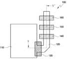
도 4는 본 발명의 일 실시예에 따른 이미지 센서의 단위 픽셀을 개략적으로 나타낸 평면도이다. 도 5는 도 4의 Ⅴ-Ⅴ' 선을 따라 절단한 단면도이다.4 is a plan view schematically illustrating a unit pixel of an image sensor according to an exemplary embodiment. FIG. 5 is a cross-sectional view taken along the line VV ′ of FIG. 4.
도 4를 참조하면, APS 어레이(도 1 및 도 2의 10 참조) 영역은 단위 픽셀 영역(100)들이 매트릭스 형태로 배열됨에 따라, 기판(101)을 사각 형태의 단위 픽셀 영역(100)들로 구분할 수 있다. 그리고 각 단위 픽셀 영역(100)의 중심에는 수광 소자(110)가 위치하며, 수광 소자(110) 주위의 각 단위 픽셀 영역(100) 내에는 플로팅 확산 영역(120), 전하 전송 소자(130), 리셋 소자(140), 드라이브 소자(150) 및 선택 소자(160)가 위치한다.Referring to FIG. 4, as the
그리고, 로직 영역에는 NMOS 및 PMOS 트랜지스터(210, 220), 커패시터 및 저항 등의 로직 소자들이 위치하여 논리 회로를 구성한다.In the logic region, logic elements such as NMOS and
도 5를 참조하면, 본 발명의 일 실시예에서 이미지 센서는 P형 벌크 기판(101a) 상에 P형 에피층(101b)이 형성된 기판(101)을 이용할 수 있다. 그리고 기판(101) 내에는 기판(101) 표면과 이격되어 P형 에피층(101b) 내에 형성된 P형 불순물 영역인 P형 딥-웰(103)이 형성되어 있을 수 있다.Referring to FIG. 5, in an embodiment of the present disclosure, the image sensor may use a
P형 딥 웰(103)은 벌크 기판(101a)의 깊은 곳에서 생성된 전하들이 수광 소자(110)로 흘러들어가지 않도록 포텐셜 배리어(potential barrier)를 형성하고, 전하와 홀의 재결합(recombination) 현상을 증가시켜 전하들의 랜덤 드리프트에 의한 화소간 크로스토크를 감소시키는 크로스토크 배리어이다.The P-type deep well 103 forms a potential barrier to prevent the charges generated in the deep portion of the
P형 딥 웰(103)은 예를 들어, 기판(101)의 표면으로부터 3 내지 12㎛ 깊이에서 최고 농도를 가지며 1 내지 5㎛의 층두께를 형성하도록 형성될 수 있다. 여기서, 3 내지 12㎛는 실리콘 내에서 적외선 또는 근적외선의 흡수 파장의 길이(absorption length of red or near infrared region light)와 실질적으로 동일하다. 여기서, P형 딥 웰(103)의 깊이는 기판(101)의 표면으로부터 얕을수록 확산 방지 효과가 크므로 크로스토크가 작아지나, 수광 소자(110)의 영역 또한 얕아지므로 깊은 곳에서 광전 변환 비율이 상대적으로 큰 장파장(예를 들어, 레드 파장)을 갖는 입사광에 대한 감도가 낮아질 수 있다. 따라서, 입사광의 파장 영역에 따라 P형 딥 웰(103)의 형성 위치는 조절될 수 있다.The P-type deep well 103 may be formed to have a highest concentration at a depth of 3 to 12 μm from the surface of the
본 발명의 일 실시예에서는 P형 벌크 기판(101a) 상에 P형 에피층(101b)이 성장되고, P형 에피층(101b) 내에 P형 딥 웰(103)이 형성되어 있는 경우만 설명하였으나, 이에 제한되는 것은 아니다. 예를 들어, P형 벌크 기판(101a) 대신 N형 벌 크 기판이 이용될 수도 있다. 그리고 P형 에피층(101b) 대신 N형 에피층이 형성될 수도 있다. 또한, 경우에 따라서는 P형 딥 웰(103)이 형성되지 않을 수도 있다. 즉, 기판(101)은 이러한 여러 가지의 조합이 가능하다.In the exemplary embodiment of the present invention, only the case where the P-
그리고, 이러한 기판(101) 내에는 활성 영역과 필드 영역을 구분하기 위한 소자 분리막(107)이 형성되어 있다. 또한, 로직 영역의 기판(101) 내에는 PMOS 트랜지스터를 형성하기 위한 N-웰(105)이 형성되어 있다.In the
한편, 이와 같은 기판(101) 상에는 다수의 게이트들이 형성되어 있다. 즉, 단위 픽셀 영역의 기판(101) 상에는 트랜스퍼 게이트(130), 리셋 게이트(140), 드라이브 게이트(150) 및 선택 게이트(160)가 위치하며, 로직 영역의 기판(101) 상에는 NMOS 및 PMOS 트랜지스터의 게이트(210, 220)가 위치할 수 있다.Meanwhile, a plurality of gates are formed on the
그리고, 단위 픽셀 영역에서 트랜스퍼 게이트(130)의 일측에는 수광 소자(110)가 위치한다. 본 발명의 일 실시예에서 수광 소자(110)로는 핀드 포토 다이오드가 형성될 수 있다.The
보다 상세히 설명하면, 핀드 포토 다이오드(110)는 2번의 이온 주입을 통해 형성된 N형 포토다이오드(112)와 P형 포토다이오드(114)를 포함한다. 여기서, N형 포토다이오드(112)는 P형 에피층(101b) 내에 깊게 형성되어 있으며, P형 포토다이오드(114)는 N형 포토다이오드(112)의 표면에 얕게 형성되어 있다.In more detail, the pinned
이에 따라 핀드 포토다이오드(110)는 P형 에피층(101b), N형 포토다이오드(112) 및 P형 포토다이오드(114)가 적층된 PNP 접합 구조를 갖는다.Accordingly, the pinned
여기서, N형 포토다이오드(112)는 입사광을 흡수하여 광전하를 축적하며, P 형 포토다이오드(114)는 열적으로 생성된 전하-전공 쌍(EHP: Electron-Hole Pair)을 줄임으로써 암전류를 방지한다. 여기서, 암전류는 실리콘의 댕글링 결함이나, 에칭 스트레스 등에 의한 기판(101)의 표면 손상으로 인해 발생할 수 있다. 따라서, 표면에서 열적으로 생성된 EHP 중에서 홀(hole)은 P형 포토다이오드(114)를 통해서 접지된 기판(101)으로 확산되고, 전자(electron)은 P형 포토다이오드(114)를 확산하는 과정에서 홀과 재결합되어 소멸될 수 있다.Here, the N-
그리고, 단위 픽셀 영역에서 트랜스퍼 게이트(130)의 타측에는 N형 불순물을 주입하여 형성된 플로팅 확산 영역(120)이 위치한다. 플로팅 확산 영역(120)은 핀드 포토다이오드(110)에 축적된 광전하를 트랜스퍼 게이트(130)를 통해 전송 받는다. 이러한 플로팅 확산 영역(120)은 저농도 및 고농도 불순물 영역(120a, 120b)으로 이루어질 수 있다. 즉, 플로팅 확산 영역(120)은 LDD(Lightly Doped Drain) 구조를 갖거나, DDD(Double Doped Drain) 구조를 가질 수 있다.The floating
이와 같이, 서로 이격된 핀드 포토다이오드(110)와 플로팅 확산 영역(120) 사이의 기판(101) 상에는 트랜스퍼 게이트(130)가 위치하며, 트랜스퍼 게이트(130)는 핀드 포토다이오드(110) 내에 축적된 광전하를 플로팅 확산 영역(120)으로 전달한다.As such, the
또한, 트랜스퍼 게이트(130)와 이격되고, 플로팅 확산 영역(120)과 인접한 기판(101) 상에는 리셋 게이트(140), 드라이브 게이트(150) 및 선택 게이트(160)가 서로 이격되어 위치한다. 이러한 리셋 게이트(140), 드라이브 게이트(150) 및 선택 게이트(160)의 일측에 LDD 구조 또는 DDD구조의 불순물 영역(170)이 위치한다.In addition, the
이러한 단위 픽셀 영역에는, 핀드 포토 다이오드(110), 플로팅 확산 영역(120), 리셋 게이트(140), 드라이브 게이트(150), 선택 게이트(160) 및 불순물 영역(170)들을 컨포말하게 덮는 절연막 패턴(312)이 형성되어 있다. 즉, 단위 픽셀 영역 상에는 트랜스퍼 게이트(130)의 상면을 제외한 구조물들의 상면을 덮는 절연막 패턴(312)이 형성되어 있다.An insulating film pattern conformally covering the pinned
여기서, 절연막 패턴(312)은 실리콘 질화막(312b)으로 이루어진 단일막일 수 있으며, 질화막(312b) 하부에 산화막(312a)을 더 포함할 수 있다. 이러한 절연막 패턴(312)은 실리사이드화 공정시 단위 픽셀 영역에 위치하는 소자들의 특성이 저하되는 것을 방지하는 역할을 할 수 있다. 구체적으로, 핀드 포토다이오드(110)로 입사되는 빛에 대한 감도를 떨어뜨리거나, 플로팅 확산 영역(120)에서 누설 전류가 증가되는 현상 등을 방지할 수 있다.The insulating
또한, 단위 픽셀 영역의 트랜스퍼 게이트(130), 리셋 게이트(140), 드라이버 게이트(150) 및 선택 게이트(160) 양측에는 스페이서(322)가 형성되어 있다. 스페이서(322)는 질화막으로만 이루어지거나, 도면에 도시된 바와 같이, 산화막(322a) 및 질화막(322b)으로 형성된 이중 스페이서일 수 있다. 그리고 게이트들(140, 150, 160)과 스페이서(322) 사이에 절연막 패턴(312)이 개재될 수 있으며, 이와 달리 게이트(140, 150, 160) 양측에 스페이서(322)가 위치하고 절연막 패턴(312)이 스페이서(322) 상에 컨포말하게 형성될 수도 있다.In addition,
그리고, 절연막 패턴(312)에 의해 노출된 트랜스퍼 게이트(130) 상면에는 실리사이드막(350a)이 형성되어 있다. 트랜스퍼 게이트(130) 상면에 형성된 실리사이 드막(350a)은 폴리실리콘으로 이루어진 게이트에 비해 낮은 광투과성을 갖는다. 따라서, 이미지 센서로 빛이 입사될 때, 트랜스퍼 게이트(130)로 빛이 입사되는 것을 감소시킨다. 이에 따라, 트랜스퍼 게이트(130) 하부의 채널 영역 및/또는 플로팅 확산 영역(120)에서 전자-홀 쌍(EHP)이 발생되어 이미지 센서의 화질이 저하되는 것을 방지할 수 있다. 즉, 픽셀 영역에서는 국부적으로 트랜스퍼 게이트(130) 상면에만 실리사이드막(350a)을 형성하는 것이, 트랜스퍼 게이트(130)를 제외한 픽셀 영역의 소자들의 감도를 떨어뜨리지 않으므로, 이미지 센서의 전기적 특성을 유지할 수 있을 것이다.The
한편, 로직 영역의 기판(101) 상에는 CMOS 트랜지스터가 위치한다. 즉, 기판(101) 상에 NMOS 트랜지스터의 게이트(210)와 PMOS 트랜지스터의 게이트(220)가 각각 위치하며, 각 게이트들(210, 220) 양측의 기판(101) 내에는 LDD 구조의 불순물 영역(230, 240)이 위치한다.On the other hand, a CMOS transistor is positioned on the
그리고, 각 게이트(210, 220)의 양측에는 제 1 및 제 2 스페이서(314, 322)가 형성되어 있다. 보다 상세히 설명하면, 게이트들(210, 220)의 양측에 L자 형태의 제 1 스페이서(314)가 위치하며, 제 1 스페이서(314) 상에 뿔 형상의 전형적인 제 2 스페이서(322)가 위치한다. 여기서 제 1 스페이서(314)는 절연막 패턴(312)과 동일층에 형성되어 있어, 산화막 스페이서(314a) 및 질화막 스페이서(314b)가 적층된 구조를 갖을 수 있다. 또한, 제 2 스페이서(322)도 제 1 스페이서(314)와 구분되도록 산화막 및 질화막의 적층 구조를 갖을 수 있다.First and
또한, 로직 영역의 각 게이트(210, 220) 및 불순물 영역(230, 240) 상면에는 컨택 저항을 줄이기 위한 실리사이드막(350b, 350c)이 형성되어 있다. 이 때, 로직 영역에 위치하는 실리사이드막(350b, 350c)은 픽셀 영역의 트랜스퍼 게이트(130) 상면에 위치하는 실리사이드막(350a)과 동일한 금속 성분으로 이루어져 있다.In addition, silicide layers 350b and 350c are formed on upper surfaces of the
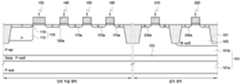
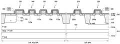
이하, 도 6 내지 도 14를 참조하여 본 발명의 일 실시예에 따른 이미지 센서의 제조 방법에 대해 상세히 설명한다. 도 6 내지 도 14는 본 발명의 일 실시예에 따른 이미지 센서의 제조 방법을 순서대로 나타낸 단면도들이다.Hereinafter, a manufacturing method of an image sensor according to an exemplary embodiment of the present invention will be described in detail with reference to FIGS. 6 to 14. 6 to 14 are cross-sectional views sequentially illustrating a method of manufacturing an image sensor according to an embodiment of the present invention.
먼저, 도 6을 참조하면, 단위 픽셀 영역과 로직 영역이 구분된 기판(101)을 준비한다. 기판(101)은 P형 벌크 기판(101a) 상에 P형 에피층(101b)이 형성된 기판(101)을 이용할 수 있다.First, referring to FIG. 6, a
그리고 나서, P형 에피층(101b) 내에 P형 불순물을 이온 주입하여 P형 딥 웰(103)을 형성한다. 딥 웰(103)은 기판(101) 표면으로부터 약 3 내지 12㎛ 깊이에서 최고 농도를 가지며, 약 1 내지 5㎛의 층 두께를 갖도록 형성할 수 있다.Then, P-type impurities are ion implanted into the P-
이어서, 로직 영역의 기판(101)에서 PMOS 트랜지스터가 형성될 소정 영역에 N형 불순물을 이온 주입하여 N-웰(105)을 형성한다.Subsequently, the N-
다음으로, LOCOS(Local Oxidation of Silicon) 공정 또는 STI(Shallow Trench Isolation) 공정을 수행하여 필드 영역과 활성 영역을 구분하는 소자 분리막(107)을 형성한다.Next, a
이 후, 기판(101) 상에 게이트 절연막 및 게이트용 도전막을 순차적으로 적층한다. 이 때, 게이트 절연막으로는 SiO2, SiON, SiN, Al2O3, Si3N4, GexOyNz, GexSiyOz 또는 고유전율 물질 등이 사용될 수 있다. 여기서, 고유전율 물질은 HfO2, ZrO2, Al2O3, Ta2O5, 하프늄 실리케이트, 지르코늄 실리케이트 또는 이들의 조합막 등을 원자층 증착법으로 형성할 수 있다. 또한, 게이트 절연막은 예시된 막질들 중에서 2종 이상의 선택된 물질을 복수 층으로 적층하여 구성될 수도 있다. 그리고, 게이트용 도전막으로는 폴리실리콘막을 증착하여 형성할 수 있다.Thereafter, the gate insulating film and the gate conductive film are sequentially stacked on the
그리고 나서, 적층된 게이트 절연막 및 게이트용 도전막을 패터닝하여, 기판(101) 상에 다수의 게이트들(130, 140, 150, 160, 210, 220)을 형성한다. 즉, 단위 픽셀 영역의 기판(101) 상에는 트랜스퍼 게이트(130), 리셋 게이트(140), 드라이버 게이트(150) 및 선택 게이트(160)를 형성하며, 로직 영역의 기판 상에는 NMOS 및 PMOS 트랜지스터의 게이트들(210, 220)을 형성한다.Thereafter, the stacked gate insulating film and the gate conductive film are patterned to form a plurality of
그리고 나서, 도 7에 도시된 바와 같이, 트랜스퍼 게이트(130) 일측의 기판(101) 내에 수광 소자(110)를 형성한다. 여기서 수광 소자(110)는 핀드 포토다이오드로 형성할 수 있다.Then, as shown in FIG. 7, the
보다 상세히 설명하면, 기판(101) 상에 핀드 포토다이오드가 형성될 영역을 노출시키는 제 1 마스크 패턴(미도시)을 형성한다. 그리고 나서, 상기 제 1 마스크 패턴을 이용하여 N형 불순물을 기판(101) 내에 이온 주입함으로써, N형 포토다이오드(112)를 형성한다. N형 포토다이오드(112)를 형성시, 트랜스퍼 게이트(130) 방향으로 0° 내지 15°의 틸트를 주어 경사지게 불순물을 이온 주입할 수 있다. 이에 따라 N형 포토다이오드(112)는 트랜스퍼 게이트(130)와 일부 오버랩될 수도 있다.In more detail, a first mask pattern (not shown) is formed on the
N형 포토다이오드(112)를 형성한 다음에는, N형 포토다이오드(112) 형성시 이용한 제 1 마스크 패턴(미도시)을 이용하여 P형 불순물을 주입함으로써, N형 포토다이오드(112) 상에 얕게 도핑된 P형 포토다이오드(114)를 형성한다. P형 포토다이오드(114) 형성시, P형 불순물을 소자 분리막(107) 방향으로 0° 이상의 틸트를 주어 경사지게 이온 주입할 수 있다. 이와 같이 형성된 P형 포토다이오드(114)는 p형 에피층(101b) 표면에서 열적으로 생성된 전자-홀 쌍(EHP)을 줄임으로써 암전류를 방지하는 역할을 한다.After the N-
이와 같이, 핀드 포토 다이오드(110)를 형성한 후, 핀드 포토 다이오드(110) 형성에 이용된 상기 제 1 마스크 패턴은 제거한다. 이상, 핀드 포토다이오드(110)는 다수의 게이트들(130, 140, 150, 160, 210, 220)을 형성한 후에 형성되는 것으로 설명하였으나, 형성 순서는 달라질 수도 있다.As described above, after the pinned
다음으로, 도 8을 참조하면, 핀드 포토다이오드(110)를 덮는 제 2 마스크 패턴을 형성한 다음, 다수의 게이트들 양측의 기판(101) 내에 저농도 불순물 영역들(120a, 170a, 230a, 240a)을 형성한다. 이 때, 단위 픽셀 영역의 저농도 불순물 영역(120a, 170a)은 N형 포토다이오드(112)와 동일한 N형 불순물을 도핑하여 형성한다. 이 때, 트랜스퍼 게이트(130)와 리셋 게이트(140) 사이에 형성된 불순물 영역(120a)은 저농도의 플로팅 확산 영역에 해당한다.Next, referring to FIG. 8, after forming a second mask pattern covering the pinned
그리고 로직 영역에서는 NMOS 트랜지스터의 게이트(210) 양측에 N형 불순물을 도핑하고, PMOS 트랜지스터의 게이트(220) 양측에 P형 불순물을 도핑하여 각각 저농도 불순물 영역(230a, 240a)을 형성한다. 여기서, P형의 불순물 영역을 형성하 기 위해 또 다른 마스크 패턴이 이용될 수 있다.In the logic region, N-type impurities are doped on both sides of the
이와 같이 저농도 불순물 영역들(120a, 170a, 230a, 240a)을 형성한 다음에는, 상기 제 2 마스크 패턴을 제거한다.After the low
다음으로, 도 9에 도시된 바와 같이, 게이트들(130, 140, 150, 160, 210, 220)이 형성된 기판(101) 전면에 결과물들의 표면을 따라 컨포말하게 절연막을 형성한다.Next, as shown in FIG. 9, an insulating film is conformally formed along the surface of the resultants on the entire surface of the
보다 상세히 설명하면, 다수의 게이트들(130, 140, 150, 160, 210, 220)이 형성된 기판(101) 상에 제 1 및 제 2 절연막(310, 320)을 순차적으로 형성할 수 있다. 이 때, 제 1 절연막(310)은 후속 공정시 핀드 포토다이오드(110)의 손상을 방지하며, 단위 픽셀 영역의 소자들이 금속 물질의 영향을 받는 것을 방지하는 블로킹막으로 이용될 수 있다. 그리고 제 2 절연막(320)은 스페이서를 형성하기 위한 스페이서용 절연막으로 이용될 수 있다.In more detail, the first and second insulating
여기서, 제 1 절연막(310)은 실리콘 질화막(310b)을 증착하여 형성할 수 있으며, 질화막(310b)을 형성하기 전, 산화막(310a)을 형성할 수도 있다. 이 때, 산화막(310a)은 열산화 공정을 통해 형성할 수 있다. 이와 같이 형성되는 산화막(310a)은 게이트 하부의 게이트 절연막의 신뢰성을 향상시키고, 게이트 형성시 식각에 의한 손상을 회복(curing)시켜 전기적 신뢰성을 향상시킬 수 있다.The first insulating
그리고, 제 2 절연막(320) 또한 제 1 절연막(310) 상에 산화막(320a) 및 질화막(320b)을 순차적으로 증착하여 형성할 수 있다.The second
이어서, 도 10을 참조하면, 제 2 절연막(320)을 이방성 식각하여 다수의 게 이트들(130, 140, 150, 160, 210, 220) 양측에 스페이서(322)를 형성한다. 스페이서(322) 형성시 제 2 절연막(320)이 산화막(320a) 및 질화막(320b)으로 이루어져 있으므로, 이방성 식각 공정시 제 1 절연막(310)의 질화막(310a)이 에치 스탑퍼(etch stopper) 역할을 할 수 있다. 이와 같이 형성된 스페이서(322)는 산화막으로 이루어진 L자형 스페이서(322a)와, 뿔 형상의 전형적인 질화막 스페이서(322b)로 이루어질 수 있다.Subsequently, referring to FIG. 10, the
이와 같이 스페이서(322)를 형성하고 나면, 게이트들(130, 140, 150, 160, 210, 220) 및 기판(101) 상면의 제 1 절연막(310)이 노출된다.After the
이상, 도 9 및 도 10을 참조하여, 제 2 절연막(320)을 이용하여 스페이서(322)를 형성하는 것으로 설명하였으나, 제 1 절연막(310)을 이용하여 게이트들(130, 140, 150, 160, 210, 220) 양측에 스페이서를 형성할 수 있으며, 스페이서를 형성한 다음, 제 2 절연막(320)을 결과물의 표면을 따라 컨포말하게 증착할 수도 있을 것이다. 이러한 경우, 스페이서 상에 형성되는 제 2 절연막(320)이 블록킹막 역할을 할 수 있다.9 and 10, the
즉, 기판(101) 및 게이트들(130, 140, 150, 160, 210, 220)을 따라 컨포말하게 형성되는 절연막은 스페이서의 하부 또는 상부에 위치할 수 있다.That is, the insulating film conformally formed along the
다음으로, 도 11을 참조하면, 게이트들(130, 140, 150, 160, 210, 220) 및 게이트들 양측에 형성된 스페이서들(322)을 이온 주입 마스크로 이용하여 기판(101) 내에 고농도 불순물 영역들(120b, 170b, 230b, 240b)을 형성한다. 보다 상세히 설명하면, 단위 픽셀 영역 및 로직 영역의 NMOS 트랜지스터 영역 내에는 N형 불순물을 이온 주입하여 N형의 고농도 불순물 영역들(120b, 170b, 230b)을 형성하고, 로직 영역의 PMOS 트랜지스터 영역 내에는 P형 불순물을 주입하여 P형의 고농도 불순물 영역(240b)을 형성한다. 이에 따라, DDD 또는 LDD 구조의 플로팅 확산 영역(120) 및 불순물 영역(170, 230, 240)들이 형성될 수 있다.Next, referring to FIG. 11, a high concentration impurity region in the
다음으로, 도 12를 참조하면, 결과물 전면에 포토레지스트막을 형성하고 패터닝하여, 단위 픽셀 영역의 트랜스퍼 게이트(130) 상부와 로직 영역을 동시에 노출시키는 마스크 패턴(330)을 형성한다. 여기서 마스크 패턴(330)은 절연막(즉, 제 1 절연막(310))을 노출시킬 수 있다.Next, referring to FIG. 12, a photoresist film is formed and patterned on the entire surface of the resultant to form a
그리고 나서, 마스크 패턴(330)을 이용하여 제 1 절연막(310)을 이방성 식각함으로써 트랜스퍼 게이트(130) 상면과, 로직 영역의 기판(101) 및 게이트들(210, 220)을 노출시킨다.Then, the first insulating
여기서, 제 1 절연막(310)을 이방성 식각하므로, 로직 영역의 게이트들(210, 220) 양측에는 다중 스페이서가 형성될 수 있다. 즉, 로직 영역의 게이트들(210, 220) 양측에는 제 1 절연막(310)으로 형성된 제 1 스페이서(314)와, 제 2 절연막(320)으로 형성된 제 2 스페이서(322)가 형성될 수 있다. 이 때, 제 1 스페이서(314)는 제 2 스페이서(322) 하부에 위치한다.Here, since the first insulating
이와 같이, 제 1 절연막(310)을 이방성 식각한 다음에는 애싱 공정을 수행하여 마스크 패턴(330)을 제거한다. 그러고 나면, 단위 픽셀 영역에는 트랜스퍼 게이트(130) 상면을 제외한 게이트들(140, 150, 160) 및 기판(101)을 컨포말하게 덮는 절연막 패턴(312)이 형성될 수 있다. 여기서, 절연막 패턴(312)은 질화막 패 턴(312b)이거나, 산화막 패턴(312a)/질화막 패턴(312b)이 적층된 구조로 이루어질 수 있다.As described above, after the anisotropic etching of the first insulating
이와 같이, 픽셀 영역에 형성된 절연막 패턴(312b)은 리셋 소자(140), 드라이버 소자(150), 선택 소자(160) 및 불순물 영역(170)들을 덮고 있으므로, 이어서 진행될 실리사이드화 공정시 리셋 소자(140), 드라이버 소자(150), 선택 소자(160) 및 불순물 영역(170)이 실리사이드화되는 것을 방지할 수 있다. 그러므로, 픽셀 영역에서 금속 물질의 영향으로 인해 누설 전류 특성이 저하되는 것을 방지할 수 있다.As described above, since the insulating
이 후, 도 13을 참조하면, 결과물 전면에 실리사이드막을 형성하기 위한 금속막(340)을 형성한다. 금속막(340)으로는 예를 들어, 코발트(Co), 티타늄(Ti), 니켈(Ni) 또는 텅스텐(W) 등이 이용될 수 있다. 금속막(340)을 증착한 다음에는 열처리 공정을 실시하여 금속막(340)과 접하는 게이트(130, 210, 220)) 및 기판(1010)의 실리콘 성분을 금속 물질과 반응시킨다.Thereafter, referring to FIG. 13, a
열처리를 통한 실리사이드화 공정시, 단위 픽셀 영역에서는 트랜스퍼 게이트(130) 상면을 제외하고 금속막(340) 하부에 절연막 패턴(312)이 개재되어 있다. 즉, 핀드 포토 다이오드(110), 플로팅 확산 영역(120), 리셋 게이트(140), 드라이버 게이트(150), 선택 게이트(160) 및 불순물 영역들(170)은 절연막 패턴(312)에 의해 덮여 있어, 상부에 실리사이드막이 형성되는 것을 방지할 수 있다. 또한, 단위 픽셀 영역에 금속막(340)을 형성함으로 인해 단위 픽셀들의 감도가 저하되는 것을 방지할 수 있다.In the silicide process through heat treatment, the insulating
이와 같이 실리사이드화 공정을 수행한 다음에는, 식각 공정을 진행하여 실리콘과 반응하지 않은 금속막을 제거한다.After the silicidation process is performed as described above, the etching process is performed to remove the metal film not reacted with silicon.
이에 따라, 도 14에 도시된 바와 같이, 트랜스퍼 게이트(130)의 상면과, 로직 영역의 게이트들(210, 220) 및 불순물 영역들(230, 240) 상면에만 실리사이드막(350a, 350b, 350c)을 형성할 수 있다.Accordingly, as shown in FIG. 14, the
이와 같이 형성된 실리사이드막(350a, 350b, 350c)은 로직 영역의 게이트(210, 220) 및 불순물 영역(230, 240)에서 콘택 저항을 줄일 수 있어, 이미지 센서의 동작을 향상시킬 수 있다. 이와 동시에, 단위 픽셀 영역에서는 트랜스퍼 게이트(130) 상면에 실리사이드막(350a)이 형성되어 있으므로, 핀드 포토다이오드(110)로 입사되는 빛이 트랜스퍼 게이트(130)로 입사되는 것을 차단할 수 있다.The
그리고, 픽셀 영역의 트랜스퍼 게이트 상면과 로직 영역을 동시에 노출시키는 절연막 패턴(312)을 이용함으로써, 서로 다른 영역에 위치하는 실리사이드막(350a, 350b, 350c)을 동시에 형성할 수 있으므로, 이미지 센서의 제조 공정이 단순화될 수 있다.In addition, by using the insulating
이상, 첨부된 도면을 참조하여 본 발명의 실시예를 설명하였지만, 본 발명이 속하는 기술분야에서 통상의 지식을 가진 자는 본 발명이 그 기술적 사상이나 필수적인 특징을 변경하지 않고서 다른 구체적인 형태로 실시될 수 있다는 것을 이해할 수 있을 것이다. 그러므로 이상에서 기술한 실시예에는 모든 면에서 예시적인 것이며 한정적이 아닌 것으로 이해해야만 한다.Although the embodiments of the present invention have been described above with reference to the accompanying drawings, those skilled in the art to which the present invention belongs may be embodied in other specific forms without changing the technical spirit or essential features of the present invention. You will understand that. Therefore, it should be understood that the embodiments described above are exemplary in all respects and not restrictive.
도 1은 본 발명의 일 실시예에 따른 이미지 센서의 블록도이다.1 is a block diagram of an image sensor according to an exemplary embodiment.
도 2는 본 발명의 실시예들에 따른 이미지 센서의 액티브 픽셀 센서(APS) 어레이의 간략 회로도이다.2 is a simplified circuit diagram of an active pixel sensor (APS) array of image sensors in accordance with embodiments of the present invention.
도 3은 본 발명의 실시예들에 따른 이미지 센서의 단위 픽셀의 회로도이다.3 is a circuit diagram of a unit pixel of an image sensor according to example embodiments.
도 4는 본 발명의 일 실시예에 따른 이미지 센서의 개략적인 평면도이다.4 is a schematic plan view of an image sensor according to an embodiment of the present invention.
도 5는 도 4의 Ⅴ-Ⅴ' 선을 따라 절단한 단면도이다.FIG. 5 is a cross-sectional view taken along the line VV ′ of FIG. 4.
도 6 내지 도 14는 본 발명의 일 실시예에 따른 이미지 센서의 제조 방법을 순서대로 나타낸 단면도들이다.6 to 14 are cross-sectional views sequentially illustrating a method of manufacturing an image sensor according to an embodiment of the present invention.
<도면의 주요 부분에 관한 부호의 설명><Explanation of symbols on main parts of the drawings>
100: 단위 픽셀101: 기판100: unit pixel 101: substrate
103: P형 딥 웰105: N-웰103: P type deep well 105: N-well
107: 소자 분리막110: 포토다이오드107: device isolation layer 110: photodiode
112: N형 포토다이오드114: P형 포토다이오드112: N-type photodiode 114: P-type photodiode
120: 플로팅 확산 영역130: 트랜스퍼 게이트120: floating diffusion region 130: transfer gate
140: 리셋 게이트150: 드라이브 게이트140: reset gate 150: drive gate
160: 선택 게이트170: 불순물 영역160: selection gate 170: impurity region
210: NMOS 게이트220: PMOS 게이트210: NMOS gate 220: PMOS gate
230, 240: 불순물 영역310: 제 1 절연막230, 240: impurity region 310: first insulating film
312: 절연막 패턴314: 제 1 스페이서312: insulating film pattern 314: first spacer
320: 제 2 절연막322: 제 2 스페이서320: second insulating film 322: second spacer
330: 마스크 패턴340: 금속막330: mask pattern 340: metal film
350a, 350b, 350c: 실리사이드막350a, 350b, 350c: silicide film
Claims (19)
Translated fromKoreanPriority Applications (2)
| Application Number | Priority Date | Filing Date | Title |
|---|---|---|---|
| KR1020070067575AKR20090003854A (en) | 2007-07-05 | 2007-07-05 | Image sensor and its manufacturing method |
| US12/213,534US20090008688A1 (en) | 2007-07-05 | 2008-06-20 | Unit pixels, image sensors and methods of manufacturing the same |
Applications Claiming Priority (1)
| Application Number | Priority Date | Filing Date | Title |
|---|---|---|---|
| KR1020070067575AKR20090003854A (en) | 2007-07-05 | 2007-07-05 | Image sensor and its manufacturing method |
Publications (1)
| Publication Number | Publication Date |
|---|---|
| KR20090003854Atrue KR20090003854A (en) | 2009-01-12 |
Family
ID=40220755
Family Applications (1)
| Application Number | Title | Priority Date | Filing Date |
|---|---|---|---|
| KR1020070067575AWithdrawnKR20090003854A (en) | 2007-07-05 | 2007-07-05 | Image sensor and its manufacturing method |
Country Status (2)
| Country | Link |
|---|---|
| US (1) | US20090008688A1 (en) |
| KR (1) | KR20090003854A (en) |
Cited By (1)
| Publication number | Priority date | Publication date | Assignee | Title |
|---|---|---|---|---|
| KR20190062272A (en)* | 2017-11-28 | 2019-06-05 | 타이완 세미콘덕터 매뉴팩쳐링 컴퍼니 리미티드 | Semiconductor device and method of manufacturing the same |
Families Citing this family (13)
| Publication number | Priority date | Publication date | Assignee | Title |
|---|---|---|---|---|
| JP4793402B2 (en)* | 2008-04-21 | 2011-10-12 | ソニー株式会社 | Solid-state imaging device, manufacturing method thereof, and electronic apparatus |
| KR101458052B1 (en)* | 2008-06-12 | 2014-11-06 | 삼성전자주식회사 | Simosa image sensor having a color mixing preventing structure and method of manufacturing the same |
| US9041841B2 (en)* | 2008-10-10 | 2015-05-26 | Taiwan Semiconductor Manufacturing Company, Ltd. | Image sensor having enhanced backside illumination quantum efficiency |
| EP2518768B1 (en)* | 2009-12-26 | 2019-03-20 | Canon Kabushiki Kaisha | Solid-state imaging device and imaging system |
| JP2012182426A (en) | 2011-02-09 | 2012-09-20 | Canon Inc | Solid state image pickup device, image pickup system using solid state image pickup device and solis state image pickup device manufacturing method |
| JP5885721B2 (en)* | 2011-02-09 | 2016-03-15 | キヤノン株式会社 | Method for manufacturing solid-state imaging device |
| KR20150077528A (en)* | 2013-12-27 | 2015-07-08 | 에스케이하이닉스 주식회사 | Transistor and method for manufacturing the same, image sensor with the same |
| US9935140B2 (en) | 2015-05-19 | 2018-04-03 | Canon Kabushiki Kaisha | Solid state imaging device, manufacturing method of solid state imaging device, and imaging system |
| US9899445B2 (en) | 2015-05-19 | 2018-02-20 | Canon Kabushiki Kaisha | Method for manufacturing solid-state image pickup apparatus, solid-state image pickup apparatus, and image pickup system including the same |
| JP6711597B2 (en)* | 2015-12-01 | 2020-06-17 | キヤノン株式会社 | Solid-state imaging device manufacturing method, solid-state imaging device, and imaging system having the same |
| US10474567B2 (en)* | 2016-05-25 | 2019-11-12 | Samsung Electronics Co., Ltd. | Multi-bit data representation framework to enable dual program operation on solid-state flash devices |
| US12033902B2 (en)* | 2021-03-19 | 2024-07-09 | Taiwan Semiconductor Manufacturing Company, Ltd. | Mid-manufacturing semiconductor wafer layer testing |
| CN115548032A (en)* | 2021-06-29 | 2022-12-30 | 中芯国际集成电路制造(北京)有限公司 | Image sensor and method of forming the same |
Family Cites Families (5)
| Publication number | Priority date | Publication date | Assignee | Title |
|---|---|---|---|---|
| US6023081A (en)* | 1997-11-14 | 2000-02-08 | Motorola, Inc. | Semiconductor image sensor |
| KR100278285B1 (en)* | 1998-02-28 | 2001-01-15 | 김영환 | Cmos image sensor and method for fabricating the same |
| KR100685875B1 (en)* | 2004-12-24 | 2007-02-23 | 동부일렉트로닉스 주식회사 | CMOS image sensor and its manufacturing method |
| TWI302754B (en)* | 2005-02-28 | 2008-11-01 | Magnachip Semiconductor Ltd | Complementary metal-oxide-semiconductor image sensor and method for fabricating the same |
| US7675097B2 (en)* | 2006-12-01 | 2010-03-09 | International Business Machines Corporation | Silicide strapping in imager transfer gate device |
- 2007
- 2007-07-05KRKR1020070067575Apatent/KR20090003854A/ennot_activeWithdrawn
- 2008
- 2008-06-20USUS12/213,534patent/US20090008688A1/ennot_activeAbandoned
Cited By (4)
| Publication number | Priority date | Publication date | Assignee | Title |
|---|---|---|---|---|
| KR20190062272A (en)* | 2017-11-28 | 2019-06-05 | 타이완 세미콘덕터 매뉴팩쳐링 컴퍼니 리미티드 | Semiconductor device and method of manufacturing the same |
| US10903336B2 (en) | 2017-11-28 | 2021-01-26 | Taiwan Semiconductor Manufacturing Co., Ltd. | Semiconductor device and method of manufacturing the same |
| US11437495B2 (en) | 2017-11-28 | 2022-09-06 | Taiwan Semiconductor Manufacturing Co., Ltd. | Semiconductor device and method of manufacturing the same |
| US12159921B2 (en) | 2017-11-28 | 2024-12-03 | Taiwan Semiconductor Manufacturing Co., Ltd. | Semiconductor device and method of manufacturing the same |
Also Published As
| Publication number | Publication date |
|---|---|
| US20090008688A1 (en) | 2009-01-08 |
Similar Documents
| Publication | Publication Date | Title |
|---|---|---|
| KR20090003854A (en) | Image sensor and its manufacturing method | |
| KR101439434B1 (en) | Image sensor and manufacturing method thereof | |
| US8344431B2 (en) | Image sensor having reduced dark current | |
| US7927902B2 (en) | Methods of fabricating image sensors and image sensors fabricated thereby | |
| KR102433575B1 (en) | Image sensor | |
| US7524695B2 (en) | Image sensor and pixel having an optimized floating diffusion | |
| US7920192B2 (en) | Photoelectric conversion device with a pixel region and a peripheral circuit region sharing a same substrate | |
| US20090179237A1 (en) | CMOS image sensor and method for fabricating the same | |
| KR100690884B1 (en) | Image sensor and its manufacturing method | |
| KR100809322B1 (en) | Image sensor manufacturing method and image sensor manufactured accordingly | |
| KR100714484B1 (en) | Image sensor and method for fabricating the same | |
| KR100725367B1 (en) | Image sensor and its manufacturing method | |
| KR100746222B1 (en) | Manufacturing Methods of Image Sensors | |
| KR20090025933A (en) | Image sensor and its manufacturing method | |
| KR20020045450A (en) | Cmos image sensor and method for fabricating the same | |
| KR100587137B1 (en) | CMOS image sensor with blocking self-aligning silicide side layer in sensing node of pixel and manufacturing method thereof | |
| KR100806786B1 (en) | Image sensor and its manufacturing method | |
| KR20090032706A (en) | CMOS image sensor | |
| KR20080062061A (en) | Image sensor and its manufacturing method |
Legal Events
| Date | Code | Title | Description |
|---|---|---|---|
| PA0109 | Patent application | Patent event code:PA01091R01D Comment text:Patent Application Patent event date:20070705 | |
| PG1501 | Laying open of application | ||
| PC1203 | Withdrawal of no request for examination | ||
| WITN | Application deemed withdrawn, e.g. because no request for examination was filed or no examination fee was paid |