KR20090002284A - Light emitting device - Google Patents
Light emitting deviceDownload PDFInfo
- Publication number
- KR20090002284A KR20090002284AKR1020070062914AKR20070062914AKR20090002284AKR 20090002284 AKR20090002284 AKR 20090002284AKR 1020070062914 AKR1020070062914 AKR 1020070062914AKR 20070062914 AKR20070062914 AKR 20070062914AKR 20090002284 AKR20090002284 AKR 20090002284A
- Authority
- KR
- South Korea
- Prior art keywords
- light emitting
- layer
- substrate
- emitting diode
- region
- Prior art date
- Legal status (The legal status is an assumption and is not a legal conclusion. Google has not performed a legal analysis and makes no representation as to the accuracy of the status listed.)
- Ceased
Links
Images


Classifications
- H—ELECTRICITY
- H01—ELECTRIC ELEMENTS
- H01L—SEMICONDUCTOR DEVICES NOT COVERED BY CLASS H10
- H01L25/00—Assemblies consisting of a plurality of semiconductor or other solid state devices
- H01L25/03—Assemblies consisting of a plurality of semiconductor or other solid state devices all the devices being of a type provided for in a single subclass of subclasses H10B, H10D, H10F, H10H, H10K or H10N, e.g. assemblies of rectifier diodes
- H01L25/04—Assemblies consisting of a plurality of semiconductor or other solid state devices all the devices being of a type provided for in a single subclass of subclasses H10B, H10D, H10F, H10H, H10K or H10N, e.g. assemblies of rectifier diodes the devices not having separate containers
- H01L25/075—Assemblies consisting of a plurality of semiconductor or other solid state devices all the devices being of a type provided for in a single subclass of subclasses H10B, H10D, H10F, H10H, H10K or H10N, e.g. assemblies of rectifier diodes the devices not having separate containers the devices being of a type provided for in group H10H20/00
- H01L25/0753—Assemblies consisting of a plurality of semiconductor or other solid state devices all the devices being of a type provided for in a single subclass of subclasses H10B, H10D, H10F, H10H, H10K or H10N, e.g. assemblies of rectifier diodes the devices not having separate containers the devices being of a type provided for in group H10H20/00 the devices being arranged next to each other
- H—ELECTRICITY
- H01—ELECTRIC ELEMENTS
- H01L—SEMICONDUCTOR DEVICES NOT COVERED BY CLASS H10
- H01L2224/00—Indexing scheme for arrangements for connecting or disconnecting semiconductor or solid-state bodies and methods related thereto as covered by H01L24/00
- H01L2224/01—Means for bonding being attached to, or being formed on, the surface to be connected, e.g. chip-to-package, die-attach, "first-level" interconnects; Manufacturing methods related thereto
- H01L2224/42—Wire connectors; Manufacturing methods related thereto
- H01L2224/47—Structure, shape, material or disposition of the wire connectors after the connecting process
- H01L2224/48—Structure, shape, material or disposition of the wire connectors after the connecting process of an individual wire connector
- H01L2224/4805—Shape
- H01L2224/4809—Loop shape
- H01L2224/48091—Arched
- H—ELECTRICITY
- H10—SEMICONDUCTOR DEVICES; ELECTRIC SOLID-STATE DEVICES NOT OTHERWISE PROVIDED FOR
- H10H—INORGANIC LIGHT-EMITTING SEMICONDUCTOR DEVICES HAVING POTENTIAL BARRIERS
- H10H20/00—Individual inorganic light-emitting semiconductor devices having potential barriers, e.g. light-emitting diodes [LED]
- H10H20/80—Constructional details
- H10H20/85—Packages
- H10H20/851—Wavelength conversion means
- Y—GENERAL TAGGING OF NEW TECHNOLOGICAL DEVELOPMENTS; GENERAL TAGGING OF CROSS-SECTIONAL TECHNOLOGIES SPANNING OVER SEVERAL SECTIONS OF THE IPC; TECHNICAL SUBJECTS COVERED BY FORMER USPC CROSS-REFERENCE ART COLLECTIONS [XRACs] AND DIGESTS
- Y10—TECHNICAL SUBJECTS COVERED BY FORMER USPC
- Y10S—TECHNICAL SUBJECTS COVERED BY FORMER USPC CROSS-REFERENCE ART COLLECTIONS [XRACs] AND DIGESTS
- Y10S362/00—Illumination
- Y10S362/80—Light emitting diode
Landscapes
- Engineering & Computer Science (AREA)
- Power Engineering (AREA)
- Microelectronics & Electronic Packaging (AREA)
- Physics & Mathematics (AREA)
- Condensed Matter Physics & Semiconductors (AREA)
- General Physics & Mathematics (AREA)
- Computer Hardware Design (AREA)
- Led Device Packages (AREA)
Abstract
Description
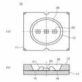
Translated fromKorean도 1의 (a)(b)는 종래 발광 다이오드 패키지의 구조를 나타낸 정면도 및 그 측 단면도.Figure 1 (a) (b) is a front view and a side cross-sectional view showing the structure of a conventional light emitting diode package.
도 2는 종래 발광 다이오드 패키지의 다른 구조를 나타낸 정면도.Figure 2 is a front view showing another structure of a conventional light emitting diode package.
도 3은 본 발명 제 1실시 예에 따른 발광 장치를 나타낸 정면도.3 is a front view showing a light emitting device according to the first embodiment of the present invention.
도 4는 도 3의 측 단면도.4 is a side cross-sectional view of FIG. 3.
도 5는 도 3의 발광 다이오드들의 전극 연결 구조를 나타낸 도면.5 is a view illustrating an electrode connection structure of the light emitting diodes of FIG. 3.
도 6은 본 발명 제 2실시 예에 따른 발광 장치를 나타낸 정면도.6 is a front view showing a light emitting device according to a second embodiment of the present invention.
도 7은 도 6의 전극 회로 구성도.FIG. 7 is a diagram illustrating an electrode circuit of FIG. 6. FIG.
〈도면의 주요 부분에 대한 부호의 설명〉<Explanation of symbols for main parts of drawing>
100,200 : 발광 다이오드 패키지100,200: LED Package
101,201 : 기판110,120,210,220 : 발광부101,201: substrate 110,120,210,220: light emitting unit
111,211 : 제 1층 영역121,221 : 제 2층 영역111,211: first layer region 121,221: second layer region
113,123,215 : 청색 발광 다이오드213 : 녹색 발광 다이오드113,123,215 Blue
223 : 적색 발광 다이오드130,132 : 몰드 부재223: red light emitting diode 130,132: mold member
119,129,219,229 : 전극패드119,129,219,229: electrode pad
117,127,217,227 : 와이어117,127,217,227: wire
본 발명은 발광 장치에 관한 것이다.The present invention relates to a light emitting device.
발광 다이오드(light emitting diode)는 GaAs, AlGaAs, GaN, InGaN 및 AlGaInP 등의 화합물 반도체 재료를 이용하여 발광 원을 구성함으로써 다양한 색을 구현할 수 있는 반도체 소자를 말한다.A light emitting diode refers to a semiconductor device capable of realizing various colors by forming a light emitting source using compound semiconductor materials such as GaAs, AlGaAs, GaN, InGaN, and AlGaInP.
일반적으로, 발광 다이오드 소자의 특성을 결정하는 기준으로는 색(color) 및 휘도, 휘도 세기의 범위 등이 있고, 이러한 발광 다이오드 소자의 특성은 1차적으로는 발광 다이오드 소자에 사용되고 있는 화합물 반도체 재료에 의해 결정되지만, 2차적인 요소로 칩을 실장하기 위한 패키지의 구조에 의해서도 큰 영향을 받는다. 고 휘도와 사용자 요구에 따른 휘도 각 분포를 얻기 위해서는 재료개발 등에 의한 1차적인 요소만으로는 한계가 있어 패키지 구조 등에 많은 관심을 갖게 되었다.In general, the criteria for determining the characteristics of the light emitting diode device include a range of color, luminance, and luminance intensity, and the characteristics of the light emitting diode device are primarily applied to the compound semiconductor material used in the light emitting diode device. It is determined by the structure of the package for mounting the chip as a secondary element, but also greatly affected. In order to obtain high luminance and angular luminance distribution according to user's demands, the primary factor due to material development is limited.
특히, 발광 다이오드는 정보 통신 기기의 소형화, 슬림화(slim) 추세에 따라 기기의 각종 부품인 저항, 콘덴서, 노이즈 필터 등은 더욱 소형화되고 있으며, PCB(Printed Circuit Board: 이하 PCB라고 함) 기판에 직접 장착된 표면실장(SMD: Surface Mount Device)형으로 만들어지고 있다. 이에 따라 표시소자로 사용되고 있는 발광 다이오드도 SMD 형으로 개발되고 있다. 이러한 SMD형의 발광 다이오드는 기존의 점등 램프를 대체할 수 있으며, 이것은 다양한 칼라를 내는 점등 표시기, 문자 표시기 및 영상 표시기 등으로 사용된다.In particular, as light emitting diodes become smaller and slimmer in information and communication equipment, various components such as resistors, capacitors, and noise filters are being further miniaturized, and are directly connected to a printed circuit board (PCB) substrate. It is made of Surface Mount Device (SMD) type. Accordingly, light emitting diodes used as display devices have also been developed as SMDs. Such SMD type light emitting diodes can replace conventional lighting lamps, which are used as lighting indicators, character indicators, and image indicators of various colors.
상기와 같이 발광 다이오드의 사용 영역이 넓어지면서, 생활에 사용되는 전등, 구조 신호용 전등 등 요구되는 휘도량이 갈수록 높아져서, 최근에는 고출력 발광 다이오드가 널리 쓰이고 있다.As the use area of the light emitting diode becomes wider as described above, the required amount of luminance such as electric light used for living and electric light for rescue signals increases gradually, and high power light emitting diodes are widely used in recent years.
도 1의 (a)(b)는 종래 발광 다이오드 패키지를 나타낸 정면도 및 그 측면도이다.Figure 1 (a) (b) is a front view and a side view showing a conventional light emitting diode package.
도 1을 참조하면, 발광 다이오드 패키지(10)의 기판(11) 상에는 반사컵(12)이 형성되며, 상기 반사컵(12) 내부에는 세 개의 청색 발광 다이오드(Blue LED)(20)가 실장되며, 상기 청색 발광 다이오드 주변에는 청색 광을 백색 광으로 여기시키는 형광체를 포함하는 투명 수지(30)가 채워진다.Referring to FIG. 1, a
이러한 발광 다이오드 패키지(10)는 하나의 패키지 내에서 단순히 백색 광만을 방출하게 되므로, 조명 또는 백 라이트 광원으로만 사용하고 있다.Since the light
그리고, 멀티 칼라를 구현하고자 할 경우, 발광 다이오드 패키지는 도 2와 같이 삼색의 발광 다이오드(Red LED, Green LED, Blue LED)(51,520,53)를 기판(41) 상에 실장한 후 투명 수지(42)를 몰딩한 후 사용하고 있다. 이때에는 삼색의 발광 다이오드(51,52,53)를 개별적으로 온/오프 구동하여 여러 가지 색의 구현이 가능하게 되므로, 지시용으로 사용하고 있다.And, in order to implement a multi-color, the light emitting diode package is a three-color light emitting diodes (Red LED, Green LED, Blue LED) (51, 520, 53) is mounted on the
종래에는 도 1 및 도 2와 같이 적색, 녹색, 청색 발광 다이오드를 선택적으로 이용하여 여러 가지의 용도로 사용할 수 있는 패키지 제품들이 요구되고 있다.Conventionally, package products that can be used for various purposes by selectively using red, green, and blue light emitting diodes as shown in FIGS. 1 and 2 are required.
본 발명은 발광 장치를 제공한다.The present invention provides a light emitting device.
또한 본 발명은 기판 내부를 복수개의 층으로 만든 후, 각 층별로 서로 다른 크기의 발광 다이오드를 실장할 수 있도록 한 발광 장치를 제공한다.In addition, the present invention provides a light emitting device in which the inside of the substrate is made of a plurality of layers, and the light emitting diodes having different sizes can be mounted for each layer.
본 발명은 백색 광의 색온도 및/또는 색 좌표 조절을 위해 각 층에 실장된 다이오드를 개별적으로 구동할 수 있도록 한 발광 장치를 제공한다.The present invention provides a light emitting device capable of individually driving a diode mounted in each layer to adjust color temperature and / or color coordinates of white light.
본 발명 실시 예에 따른 발광 장치는, 내부에 계단 형상의 다층 영역이 형성된 기판; 상기 기판의 다층 영역에 복수개의 발광 다이오드가 실장된 발광부를 포함한다.According to an embodiment of the present invention, a light emitting device includes: a substrate having a multi-layered region formed therein; The light emitting unit includes a plurality of light emitting diodes mounted in a multilayer area of the substrate.
또한 본 발명 실시 예에 따른 발광 다이오드 패키지는 내부에 계단 형상의 다층 영역이 형성된 기판; 상기 다층 영역의 제 1층 영역에 배치된 제 1청색 발광 다이오드를 갖는 제 1발광부; 상기 다층 영역의 제 2층 영역에 배치되며, 상기 제 1청색 발광 다이오드 보다 작은 크기를 갖는 제 2청색 발광 다이오드를 갖는 제 2발광부를 포함한다.In addition, a light emitting diode package according to an embodiment of the present invention includes a substrate having a multi-layered region having a stepped shape therein; A first light emitting unit having a first blue light emitting diode disposed in the first layer region of the multilayer region; And a second light emitting part disposed in the second layer area of the multilayer area and having a second blue light emitting diode having a size smaller than that of the first blue light emitting diode.
또한 본 발명 실시 예에 따른 발광 다이오드 패키지는 내부에 계단 형상의 다층 영역이 형성된 기판; 상기 다층 영역의 제 1층 영역에 배치되며 녹색 발광 다이오드를 갖는 제 1발광부; 상기 다층 영역의 제 2층 영역에 배치되며 상기 발광 다이오드 보다 작은 크기를 갖는 적색/청색 발광 다이오드를 갖는 제 2발광부를 포함한다.In addition, a light emitting diode package according to an embodiment of the present invention includes a substrate having a multi-layered region having a stepped shape therein; A first light emitting part disposed in the first layer area of the multilayer area and having a green light emitting diode; And a second light emitting part disposed in the second layer area of the multilayer area and having a red / blue light emitting diode having a smaller size than the light emitting diode.
이하에서 첨부된 도면을 참조하여 본 발명의 실시 예에 따른 발광 장치에 대하여 상세히 설명한다.Hereinafter, a light emitting device according to an exemplary embodiment will be described in detail with reference to the accompanying drawings.
도 3은 본 발명 실시 예에 따른 발광 다이오드 패키지(100)의 구조를 도시한 상측 단면도이고, 도 4는 본 발명의 실시 예에 따른 LED 패키지(100)의 구조를 도시한 측 단면도이다.3 is a top cross-sectional view showing the structure of the
도 3 및 도 4를 참조하면, 발광 다이오드 패키지(100)는 기판(101), 기판 내부의 제 1 발광부(110) 및 제 2발광부(120)를 포함한다.3 and 4, the
상기 기판(101)은 패키지 몸체를 구성하는 것으로서, 내부에 탑층(top layer)에서 계단 형상으로 식각된 다층 영역이 형성되어 있다. 여기서, 상기 다층 영역은 1층 이상으로 형성될 수 있다.The
상기 기판(101)은 다각 형상을 갖는 다면체(예: 직육면체) 또는 원(타원) 기둥 형상으로 형성될 수 있다. 이러한 기판(101)의 재질은 실리콘(silicon)이나 실리콘 카바이드(silicon carbide : SiC), 질화 알루미늄(aluminum nitride ; AlN) 등의 세라믹이나 폴리프탈아마이드(poly phthal amide : PPA), 고분자액정(Liquid Crystal Polymer : LCP) 등의 열 경화성 수지 중 어느 하나 또는 몇 가지의 혼합 재질로 이루어질 수 있다.The
상기 기판(101)의 다층 영역 중에서 가장 깊은 층을 제 1층 영역(111)이라 하고, 상기 제 1층 영역의 위 층 영역을 제 2층 영역(121)이라 한다. 상기 제 1층 영역(111)은 제 2층 영역(121)의 중앙 또는 좌/우 측에 형성될 수 있다. 또한 제 1 층 영역 및 제 2층 영역의 위치가 반대로 형성될 수 도 있다.The deepest layer among the multilayered regions of the
이때, 제 1층 영역(111)은 기판(101)의 높이의 1/2 이상 또는 최소 150um±5 이상의 깊이로 식각되며, 상기 제 1층 영역(111) 및 제 2층 영역(121) 둘레면에 형성되는 반사판(115,125)은 경사지게 형성되는 데, 예컨대 각 층의 바닥면과 반사판(115,125)이 이루는 각도는 125±2도로 형성될 수 있다.In this case, the
상기 제 1발광부(110)는 제 1층 영역(111)에 형성되며, 제 2발광부(120)는 제 2층 영역(121)에 형성된다. 상기 제 1 발광부(110)와 제 2발광부(120)에는 서로 다른 크기의 발광 다이오드들이 실장되며, 그 실장되는 발광 다이오드의 종류가 서로 같거나 다를 수도 있다. 여기서, 상기 발광 다이오드는 GaAs, AlGaAs, GaN, InGaN 및 AlGaInP 등의 화합물 반도체 재료를 이용하여 발광 원을 구성할 수 있다.The first
구체적으로 설명하면, 상기 제 1발광부(110)는 제 1층 영역(111)에서 백색 광을 방출한다. 이를 위해, 제 1청색 발광 다이오드(Blue LED)(113) 및 몰드 부재(130)를 포함하며, 상기 제 1청색 발광 다이오드(113)는 하나 이상이 제 1층 영역(111)의 바닥면 중심에 실장될 수 있으며, 상기 몰드 부재(132)는 형광체(미도시)가 혼합된 실리콘 또는 에폭시 수지가 제 1층 영역(111)에 채워진다.In detail, the first
이러한 제 1발광부(110)는 제 1청색 발광 다이오드(113)에서 발생되는 청색 광과 형광체에서 여기된 광이 혼색되어 백색 광으로 출력된다.The first
여기서, 상기 제 1청색 발광 다이오드(113)는 각각이 어느 하나의 전극 패드(119)에 도전성 접착제에 의해 접착되고, 와이어(117)를 이용하여 본딩된다. 여기서, 상기 제 1청색 발광 다이오드(113)의 실장 방식은 다이 본딩 또는 플립 칩 본딩으로 구현할 수도 있다.Here, each of the first blue
여기서, 상기 제 1발광부(110)는 제 1층 영역(111)에 백색 발광 다이오드와 투명 몰드 부재로 구성하여, 백색 광이 방출되게 할 수도 있다.The first
한편, 상기 제 2발광부(120)는 제 2층 영역(121)에서 청색 광을 방출한다. 이를 위해, 제 2청색 발광 다이오드(Blue LED)(123) 및 몰드 부재(132)를 포함하며, 상기 제 2청색 발광 다이오드(123)는 제 2층 영역(121)의 각 코너 또는 각 측 변의 중심 위치에 배치될 수 있다. 상기 몰드 부재(132)는 투명한 실리콘 또는 에폭시 수지가 제 2층 영역(121)에 채워진다.Meanwhile, the second
여기서, 제 2청색 발광 다이오드(123)는 각각이 어느 하나의 전극 패드(129)에 도전성 접착제에 의해 접착되고, 와이어(127)로 본딩된다. 여기서, 상기 제 2청색 발광 다이오드(123)의 실장 방식은 플립 칩 또는 다이 본딩 방식으로 구현할 수도 있다.Here, each of the second blue
한편, 상기 제 1발광부(110)의 제 1청색 발광 다이오드(113)와 제 2발광부(120)의 제2 청색 발광 다이오드(123)는 서로 다른 크기로 형성될 수 있다. 예를 들면, 제 1청색 발광 다이오드(113)의 한 변의 길이가 제 2청색 발광 다이오드(123)의 한 변의 길이 보다 2배 이상으로 형성될 수 있다. 또한, 상기 제 2청색 발광 다이오드(123)의 전체 합 크기로 제 1청색 발광 다이오드로 배치할 수 있다. 예컨대, 제 2청색 발광 다이오드(123)가 4개 배치될 경우 제 1청색 발광 다이오드(113)는 제 2청색 발광 다이오드(123)의 크기 보다 4배 정도 크게 형성되게 할 수 있다.Meanwhile, the first blue
그리고, 발광 다이오드 패키지(100)의 제조 방법을 보면, 기판 내부에 제 1 및 제 2층 영역(111,121)을 형성한 후, 상기 제 1층 영역(111)에는 제 1청색 발광 다이오드(113)가 실장되고, 제 2층 영역(121)에는 제 2청색 발광 다이오드(123)가 실장된다.In the manufacturing method of the
상기 기판 외부에는 복수개의 전극부(102,103)가 형성되며, 내부 회로 패턴에 의해 전극부(102,103)의 개수는 변경될 수 있다.A plurality of
이후, 상기 제 1층 영역(111)에 황색 형광체를 포함하는 몰드 부재(130)를 채워 경화시킨 후, 상기 제 2층 영역(121)에 투명 몰드 부재(132)를 채워 경화시켜 준다. 이에 따라 발광 다이오드 패키지가 완성된다.Thereafter, the
이러한 발광 다이오드 패키지(100)는 기판(101) 위에 볼록 렌즈나 평판형 프레넬 렌즈(fresnel lens) 등을 부착하여, 방출되는 광의 지향 특성을 변경할 수도 있다. 또는 이러한 렌즈 특징을 제 2층 영역(121)에 채워지는 몰드 부재(132)의 표면에 일체로 형성할 수도 있다.The light emitting
이와 같이, 제 1발광부(110)에서 방출되는 백색 광을 제 2발광부(120)에서 방출되는 청색 광을 이용하여 색 온도를 조절할 수 있으며, 또 제 2발광부(120)의 제 2청색 발광 다이오드(123)의 구동 개수에 따라 색 온도 제어가 가능하게 된다.As such, the color temperature of the white light emitted from the
또한 본 발명은 제 2발광부(120)에 제 2청색 발광 다이오드(123)와 형광체가 포함된 몰드 부재로 구성하여, 제 1발광부(110) 및 제 2발광부(120)로부터 방출되는 백색 광의 광도를 증가시켜 줄 수 있다.In addition, the present invention is composed of a mold member including the second blue
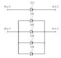
도 5는 본 발명에 따른 발광 다이오드 패키지의 전극부 구성 예를 나타낸 도면이다. 기판 내부의 회로 패턴에 의해 2 ~ 10개의 전극 단자로 구성할 수 있다. 본 발명은 도 5와 같이 4개의 전극 단자로 구성하여, 도 1에 도시된 제 1발광부(110)의 제 1청색 발광 다이오드(113)의 구동 제어 동작과, 제 2발광부(120)의 제 2청색 발광 다이오드(123)의 구동 제어 동작을 개별적으로 할 수 있다.5 is a view showing an example of the configuration of the electrode portion of the LED package according to the present invention. By the circuit pattern inside a board | substrate, it can comprise with 2-10 electrode terminals. The present invention is composed of four electrode terminals as shown in Fig. 5, the drive control operation of the first blue
또한 발광 다이오드별로 양 전극 단자를 구성하여 모든 발광 다이오드를 개별적으로 제어할 수도 있다. 예를 들면, 백색 광을 발광하기 위해 제 1청색 발광 다이오드(113)를 온 시킨 후, 다수개의 제 2청색 발광 다이오드를 차례대로 온 시켜 주어, 발광 다이오드 패키지의 연색성을 개선하고 색 온도를 조절할 수 있다. 이러한 전극 단자의 구성은 도 2에 도시된 기판의 각 층 영역을 전기적으로 연결해 주는 비아 홀(134)의 연결 패턴에 따라 변경해 줄 수 있다.In addition, each of the light emitting diodes may be configured with both electrode terminals to individually control all the light emitting diodes. For example, after the first blue
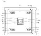
도 6은 본 발명 실시 예에 따른 발광 다이오드 패키지의 다른 예이다. 이러한 실시 예는 도 3의 실시 예와 중복 되는 부분의 설명은 배제하고 설명하기로 한다.6 is another example of a light emitting diode package according to an exemplary embodiment of the present invention. Such an embodiment will be described with the description of the overlapping part with the embodiment of FIG. 3.
도 6을 참조하면, 발광 다이오드 패키지(200)는 기판(201), 제 1발광부(210) 및 제 2발광부(220)를 포함한다.Referring to FIG. 6, the
상기 제 1발광부(210)는 기판(201)의 제 1층 영역(211)에 형성되는데, 상기 제 1층 영역(211)에는 녹색 발광 다이오드(213)가 도전성 접착제에 의해 실장되며, 와이어(217) 또는 플립 칩 방식에 의해 전극 패드(219)와 전기적으로 연결된다.The first
상기 제 2발광부(220)는 기판(201)의 제 2층 영역(221)에 의해 형성되는데, 상기 제 2층 영역(221)에는 복수개의 적색 및 청색 발광 다이오드(223,225)가 실장되며, 각 다이오드들은 도전성 접착제에 의해 어느 하나의 전극 패드(229)에 실장되며, 와이어(227) 또는 플립칩 방식에 의해 전극패드(229)와 전기적으로 연결된다.The second
이때의 적색 발광 다이오드(223)와 녹색 발광 다이오드(225)는 각각이 서로 마주보는 위치(또는 대각선 위치)에 배치된다. 이러한 배치 순서는 광 효율을 위해 변경될 수도 있다.At this time, the red
이러한 제 1 층 영역(211) 및 제 2층 영역(221)에는 몰드 부재(미도시)가 채워지는 데, 상기 몰드 부재는 투명한 에폭시 또는 실리콘 등의 수지 재질로 이루어질 수 있다.A mold member (not shown) is filled in the
그리고 상기 제 1발광부(210)의 녹색 발광 다이오드(213)는 제 2층 영역(221)에 실장된 다이오드(223,225)의 크기 보다 2배 이상으로 형성될 수 있다. 또는 그 역으로 적색 또는 청색 발광 다이오드(223,225)가 녹색 발광 다이오드 보다 1/2배로 형성될 수 있다.In addition, the green
또한, 녹색 발광 다이오드(213)는 적색 또는/및 녹색 발광 다이오드(223,225)의 크기 합에 비례하는 크기로 형성될 수 있다. 또는 녹색 발광 다이오드(213)의 최대 크기는 제 2층 영역(221)에 실장되는 발광 다이오드(223,225)의 크기 합 이하로 형성될 수 있다.In addition, the green
상기 기판(201) 외측에는 상기 전극 패드(219,229)의 구성에 따라 복수개의 전극부(202,203)가 형성될 수 있다. 도 6 및 도 7에 도시된 바와 같이, 전극부의 구성은 녹색 발광 다이오드(213)에 2개의 전극 단자를 구성하고, 적색 및 청색 발광 다이오드(223,225)를 공통으로 연결하여 2개의 전극 단자를 구성하여, 층별로 개별 구동할 수 있다. 이러한 발광 다이오드들의 구동 방식은 전극 단자를 개별적으로 인출하는지, 다이오드 종류 별로 인출하는지, 층별로 인출하는지에 따라 구동 방식이 변경될 수 있다.A plurality of
이러한 발광 다이오드 패키지(200)는 서로 다른 크기를 갖는 녹색 발광 다이오드(213)와 함께 복수개의 적색/청색 발광 다이오드(223,225)를 선택적으로 구동함에 따라 색 온도 및 색 좌표를 조절할 수 있게 된다.The light emitting
이상에서 본 발명에 대하여 실시 예를 중심으로 설명하였으나 이는 단지 예시일 뿐 본 발명을 한정하는 것이 아니며, 본 발명이 속하는 분야의 통상의 지식을 가진 자라면 본 발명의 본질적인 특성을 벗어나지 않는 범위에서 이상에 예시되지 않은 여러 가지의 변형과 응용이 가능함을 알 수 있을 것이다. 예를 들어, 본 발명의 실시예에 구체적으로 나타난 각 구성 요소는 변형하여 실시할 수 있는 것이다. 그리고 이러한 변형과 응용에 관계된 차이점들은 첨부된 청구 범위에서 규정하는 본 발명의 범위에 포함되는 것으로 해석되어야 할 것이다.Although the present invention has been described above with reference to the embodiments, these are only examples and are not intended to limit the present invention, and those skilled in the art to which the present invention pertains may have an abnormality within the scope not departing from the essential characteristics of the present invention. It will be appreciated that various modifications and applications are not illustrated. For example, each component specifically shown in the embodiment of the present invention can be modified. And differences relating to such modifications and applications will have to be construed as being included in the scope of the invention defined in the appended claims.
본 발명 실시 예에 따른 발광 장치에 의하면, 기판의 서로 다른 층 영역에 서로 다른 크기를 갖는 발광 다이오드를 배치하여, 백색 광의 색 온도 및 색 좌표 를 조절할 수 있는 효과가 있다.According to the light emitting device according to the exemplary embodiment of the present invention, light emitting diodes having different sizes are disposed in different layer regions of the substrate, thereby controlling color temperature and color coordinates of white light.
또한 연색성을 부분을 개선한 고 휘도의 발광 다이오드 패키지를 제공할 수 있다.In addition, it is possible to provide a high brightness light emitting diode package having improved color rendering.
Claims (20)
Translated fromKoreanPriority Applications (2)
| Application Number | Priority Date | Filing Date | Title |
|---|---|---|---|
| KR1020070062914AKR20090002284A (en) | 2007-06-26 | 2007-06-26 | Light emitting device |
| US12/145,252US8089079B2 (en) | 2007-06-26 | 2008-06-24 | Light emitting device |
Applications Claiming Priority (1)
| Application Number | Priority Date | Filing Date | Title |
|---|---|---|---|
| KR1020070062914AKR20090002284A (en) | 2007-06-26 | 2007-06-26 | Light emitting device |
Publications (1)
| Publication Number | Publication Date |
|---|---|
| KR20090002284Atrue KR20090002284A (en) | 2009-01-09 |
Family
ID=40159300
Family Applications (1)
| Application Number | Title | Priority Date | Filing Date |
|---|---|---|---|
| KR1020070062914ACeasedKR20090002284A (en) | 2007-06-26 | 2007-06-26 | Light emitting device |
Country Status (2)
| Country | Link |
|---|---|
| US (1) | US8089079B2 (en) |
| KR (1) | KR20090002284A (en) |
Cited By (1)
| Publication number | Priority date | Publication date | Assignee | Title |
|---|---|---|---|---|
| WO2013032177A3 (en)* | 2011-08-30 | 2013-04-25 | 엘지이노텍 주식회사 | Light-emitting device package capable of controlling color temperature |
Families Citing this family (25)
| Publication number | Priority date | Publication date | Assignee | Title |
|---|---|---|---|---|
| US8452402B2 (en)* | 2008-04-23 | 2013-05-28 | Medtronic, Inc. | Optical sensing device for use in a medical device |
| JP5308773B2 (en)* | 2008-10-30 | 2013-10-09 | スタンレー電気株式会社 | Semiconductor light emitting device |
| JP5269623B2 (en)* | 2009-01-09 | 2013-08-21 | パナソニック株式会社 | Lighting device |
| KR101064098B1 (en) | 2009-02-23 | 2011-09-08 | 엘지이노텍 주식회사 | Light emitting device package and manufacturing method thereof |
| CN101968169A (en)* | 2010-08-05 | 2011-02-09 | 深圳市众明半导体照明有限公司 | Warm white LED lamp with high brightness and high color rendering index |
| TWI446578B (en)* | 2010-09-23 | 2014-07-21 | Epistar Corp | Light-emitting element and its manufacturing method |
| JP2012114116A (en)* | 2010-11-19 | 2012-06-14 | Olympus Corp | Light emitting device |
| US8735913B2 (en)* | 2011-04-01 | 2014-05-27 | Visera Technologies Company Limited | Light emitting semiconductor structure |
| KR20120119395A (en)* | 2011-04-21 | 2012-10-31 | 삼성전자주식회사 | Light emitting device package and method of manufacturing the same |
| CN102543987A (en)* | 2012-02-07 | 2012-07-04 | 达亮电子(苏州)有限公司 | Solid-state light-emitting component |
| DE102013201952A1 (en) | 2013-02-06 | 2014-08-21 | Osram Gmbh | Semiconductor light-emitting module has substrate whose front side is arranged with semiconductor light sources that are laterally surrounded with circumferential side wall |
| TWM458672U (en)* | 2013-04-10 | 2013-08-01 | Genesis Photonics Inc | Light source module |
| US20170271548A1 (en)* | 2013-06-26 | 2017-09-21 | Epistar Corporation | Light-emitting device and manufacturing method thereof |
| KR20180036798A (en)* | 2013-06-26 | 2018-04-09 | 에피스타 코포레이션 | Light-emitting device |
| JP6268636B2 (en)* | 2014-01-08 | 2018-01-31 | パナソニックIpマネジメント株式会社 | Light emitting device, illumination light source, and illumination device |
| JP6862141B2 (en)* | 2015-10-14 | 2021-04-21 | エルジー イノテック カンパニー リミテッド | Light emitting element package and lighting equipment |
| US20170210283A1 (en)* | 2016-01-22 | 2017-07-27 | Mitsunori Ishida | Display device of operation state of automobile brake |
| DE102016104202A1 (en)* | 2016-03-08 | 2017-09-14 | Osram Opto Semiconductors Gmbh | Optoelectronic semiconductor device |
| DE102016111790A1 (en)* | 2016-06-28 | 2017-12-28 | Osram Opto Semiconductors Gmbh | Process for the production of optoelectronic semiconductor components |
| DE102017102619B4 (en)* | 2017-02-09 | 2022-10-06 | OSRAM Opto Semiconductors Gesellschaft mit beschränkter Haftung | LED unit and LED module |
| KR102304400B1 (en)* | 2017-03-20 | 2021-09-24 | 제이드 버드 디스플레이(상하이) 리미티드 | Fabrication of semiconductor devices by stacking micro LED layers |
| CN107561771A (en)* | 2017-07-31 | 2018-01-09 | 安徽芯瑞达科技股份有限公司 | Side-edge type backlight based on cup type LED lamp bead of sinking |
| CN111584467A (en)* | 2019-02-19 | 2020-08-25 | 江苏罗化新材料有限公司 | A color temperature adjustable LED light source and LED desk lamp |
| KR20220044034A (en)* | 2020-09-29 | 2022-04-06 | 삼성디스플레이 주식회사 | Display device and method of fabricating the same |
| FR3131363B1 (en)* | 2021-12-26 | 2023-11-17 | Valeo Vision | Motor vehicle signaling device |
Family Cites Families (5)
| Publication number | Priority date | Publication date | Assignee | Title |
|---|---|---|---|---|
| JPH11311721A (en)* | 1998-02-27 | 1999-11-09 | Oki Electric Ind Co Ltd | Optical coupling module and its manufacture |
| US6861675B2 (en)* | 2002-06-28 | 2005-03-01 | Kabushiki Kaisha Toshiba | Optically coupled semiconductor device and method for manufacturing the same |
| JP2005079385A (en)* | 2003-09-01 | 2005-03-24 | Toshiba Corp | Optical semiconductor device and optical signal input / output device |
| JP4535928B2 (en)* | 2005-04-28 | 2010-09-01 | シャープ株式会社 | Semiconductor light emitting device |
| KR101241528B1 (en)* | 2006-09-25 | 2013-03-08 | 엘지이노텍 주식회사 | Light Emitting device |
- 2007
- 2007-06-26KRKR1020070062914Apatent/KR20090002284A/ennot_activeCeased
- 2008
- 2008-06-24USUS12/145,252patent/US8089079B2/ennot_activeExpired - Fee Related
Cited By (2)
| Publication number | Priority date | Publication date | Assignee | Title |
|---|---|---|---|---|
| WO2013032177A3 (en)* | 2011-08-30 | 2013-04-25 | 엘지이노텍 주식회사 | Light-emitting device package capable of controlling color temperature |
| US8952407B2 (en) | 2011-08-30 | 2015-02-10 | Lg Innotek Co., Ltd. | Lighting device |
Also Published As
| Publication number | Publication date |
|---|---|
| US20090001392A1 (en) | 2009-01-01 |
| US8089079B2 (en) | 2012-01-03 |
Similar Documents
| Publication | Publication Date | Title |
|---|---|---|
| KR20090002284A (en) | Light emitting device | |
| KR101241528B1 (en) | Light Emitting device | |
| JP6648048B2 (en) | LED package and manufacturing method thereof | |
| KR101134752B1 (en) | LED Package | |
| US7977699B2 (en) | Light emitting device package and manufacture method of light emitting device package | |
| CN102646782B (en) | Light-emitting device | |
| KR100550750B1 (en) | Light emitting diode package and manufacturing method thereof | |
| JP2004356116A (en) | Light emitting diode | |
| KR20090002319A (en) | Light emitting diode package and manufacturing method thereof | |
| JP2008235824A5 (en) | ||
| CN102646777A (en) | Light emitting device package and manufacturing method thereof | |
| TWI388069B (en) | Top view type and side view type light emitting diode | |
| JP2001298216A (en) | Surface mount type semiconductor light emitting device | |
| JP2000349345A (en) | Semiconductor light emitting device | |
| KR20050029384A (en) | Light emitting diode package and method for manufacturing light emitting diode package | |
| KR101195430B1 (en) | White light emitting device and white light source module using the same | |
| KR101683888B1 (en) | Light emitting apparatus and display apparatus having the same | |
| JP2004288827A (en) | Led lamp | |
| CN104241262A (en) | Light-emitting device and display device | |
| CN100424872C (en) | Light source structure of white light LED | |
| JP2012015558A (en) | Light emitting diode package and method of manufacturing the same | |
| KR100990647B1 (en) | White light emitting device and white light source module using same | |
| KR20150009762A (en) | Light Emitting Diode Package | |
| WO2013027413A1 (en) | Protection element and light emitting device using same | |
| KR100999712B1 (en) | Light emitting diode package |
Legal Events
| Date | Code | Title | Description |
|---|---|---|---|
| PA0109 | Patent application | Patent event code:PA01091R01D Comment text:Patent Application Patent event date:20070626 | |
| PG1501 | Laying open of application | ||
| A201 | Request for examination | ||
| PA0201 | Request for examination | Patent event code:PA02012R01D Patent event date:20120626 Comment text:Request for Examination of Application Patent event code:PA02011R01I Patent event date:20070626 Comment text:Patent Application | |
| E902 | Notification of reason for refusal | ||
| PE0902 | Notice of grounds for rejection | Comment text:Notification of reason for refusal Patent event date:20130318 Patent event code:PE09021S01D | |
| E601 | Decision to refuse application | ||
| PE0601 | Decision on rejection of patent | Patent event date:20130829 Comment text:Decision to Refuse Application Patent event code:PE06012S01D Patent event date:20130318 Comment text:Notification of reason for refusal Patent event code:PE06011S01I |