KR20090001169A - LED packages and arrays thereof - Google Patents
LED packages and arrays thereofDownload PDFInfo
- Publication number
- KR20090001169A KR20090001169AKR20070065358AKR20070065358AKR20090001169AKR 20090001169 AKR20090001169 AKR 20090001169AKR 20070065358 AKR20070065358 AKR 20070065358AKR 20070065358 AKR20070065358 AKR 20070065358AKR 20090001169 AKR20090001169 AKR 20090001169A
- Authority
- KR
- South Korea
- Prior art keywords
- led
- led package
- packages
- substrate
- package
- Prior art date
- Legal status (The legal status is an assumption and is not a legal conclusion. Google has not performed a legal analysis and makes no representation as to the accuracy of the status listed.)
- Withdrawn
Links
- 238000003491arrayMethods0.000title1
- 239000000758substrateSubstances0.000claimsabstractdescription43
- 238000005476solderingMethods0.000claimsdescription9
- 238000000034methodMethods0.000claimsdescription8
- 238000007789sealingMethods0.000description4
- OAICVXFJPJFONN-UHFFFAOYSA-NPhosphorusChemical compound[P]OAICVXFJPJFONN-UHFFFAOYSA-N0.000description2
- 239000004954PolyphthalamideSubstances0.000description2
- 229920006375polyphtalamidePolymers0.000description2
- 239000010409thin filmSubstances0.000description2
- RYGMFSIKBFXOCR-UHFFFAOYSA-NCopperChemical compound[Cu]RYGMFSIKBFXOCR-UHFFFAOYSA-N0.000description1
- 239000004593EpoxySubstances0.000description1
- 239000000853adhesiveSubstances0.000description1
- 230000001070adhesive effectEffects0.000description1
- 238000005452bendingMethods0.000description1
- 239000003086colorantSubstances0.000description1
- 229910052802copperInorganic materials0.000description1
- 239000010949copperSubstances0.000description1
- 238000010586diagramMethods0.000description1
- 238000005538encapsulationMethods0.000description1
- 238000005516engineering processMethods0.000description1
- 239000004973liquid crystal related substanceSubstances0.000description1
- 238000004519manufacturing processMethods0.000description1
- 239000011159matrix materialSubstances0.000description1
- 239000002184metalSubstances0.000description1
- 229910052751metalInorganic materials0.000description1
- 239000007769metal materialSubstances0.000description1
- 238000007747platingMethods0.000description1
- 229920001690polydopaminePolymers0.000description1
- 229920001296polysiloxanePolymers0.000description1
- 238000007639printingMethods0.000description1
- 229920005989resinPolymers0.000description1
- 239000011347resinSubstances0.000description1
Images


Classifications
- H—ELECTRICITY
- H01—ELECTRIC ELEMENTS
- H01L—SEMICONDUCTOR DEVICES NOT COVERED BY CLASS H10
- H01L2224/00—Indexing scheme for arrangements for connecting or disconnecting semiconductor or solid-state bodies and methods related thereto as covered by H01L24/00
- H01L2224/01—Means for bonding being attached to, or being formed on, the surface to be connected, e.g. chip-to-package, die-attach, "first-level" interconnects; Manufacturing methods related thereto
- H01L2224/42—Wire connectors; Manufacturing methods related thereto
- H01L2224/47—Structure, shape, material or disposition of the wire connectors after the connecting process
- H01L2224/48—Structure, shape, material or disposition of the wire connectors after the connecting process of an individual wire connector
- H01L2224/4805—Shape
- H01L2224/4809—Loop shape
- H01L2224/48091—Arched
- H—ELECTRICITY
- H01—ELECTRIC ELEMENTS
- H01L—SEMICONDUCTOR DEVICES NOT COVERED BY CLASS H10
- H01L2224/00—Indexing scheme for arrangements for connecting or disconnecting semiconductor or solid-state bodies and methods related thereto as covered by H01L24/00
- H01L2224/01—Means for bonding being attached to, or being formed on, the surface to be connected, e.g. chip-to-package, die-attach, "first-level" interconnects; Manufacturing methods related thereto
- H01L2224/42—Wire connectors; Manufacturing methods related thereto
- H01L2224/47—Structure, shape, material or disposition of the wire connectors after the connecting process
- H01L2224/48—Structure, shape, material or disposition of the wire connectors after the connecting process of an individual wire connector
- H01L2224/481—Disposition
- H01L2224/48151—Connecting between a semiconductor or solid-state body and an item not being a semiconductor or solid-state body, e.g. chip-to-substrate, chip-to-passive
- H01L2224/48221—Connecting between a semiconductor or solid-state body and an item not being a semiconductor or solid-state body, e.g. chip-to-substrate, chip-to-passive the body and the item being stacked
- H01L2224/48245—Connecting between a semiconductor or solid-state body and an item not being a semiconductor or solid-state body, e.g. chip-to-substrate, chip-to-passive the body and the item being stacked the item being metallic
- H01L2224/48247—Connecting between a semiconductor or solid-state body and an item not being a semiconductor or solid-state body, e.g. chip-to-substrate, chip-to-passive the body and the item being stacked the item being metallic connecting the wire to a bond pad of the item
Landscapes
- Led Device Packages (AREA)
Abstract
Translated fromKoreanDescription
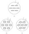
Translated fromKorean도 1 은 종래의 LED 패키지 어레이를 설명하기 위한 도면.1 is a view for explaining a conventional LED package array.
도 2 는 본 발명의 실시예에 따른 LED 패키지의 평면도.2 is a plan view of an LED package according to an embodiment of the present invention.
도 3 은 도 2의 X-X를 따라 취해진 단면도.3 is a sectional view taken along X-X of FIG. 2;
도 4 는 도 2에 도시된 LED 패키지의 저면도.4 is a bottom view of the LED package shown in FIG. 2.
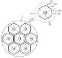
도 5 는 본 발명의 실시예에 따른 LED 패키지 어레이를 설명하기 위한 도면.5 is a view for explaining an LED package array according to an embodiment of the present invention.
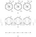
도 6 은 본 발명이 적용되는 LED 패키지의 적용예를 도시한 도면.Figure 6 is a view showing an application example of the LED package to which the present invention is applied.
도 7 은 본 발명이 적용되는 다른 실시예의 LED 패키지 어레이를 설명하기 위한 도면.7 is a view for explaining an LED package array of another embodiment to which the present invention is applied.
<도면 주요 부분에 대한 부호의 설명><Explanation of symbols for the main parts of the drawings>
10 : 기판 20 : LED 패키지10: substrate 20: LED package
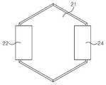
21 : 하우징 21a : 정육각형의 상부면21
21b : 측면 22 : 제 1 리드프레임21b: side 22: first leadframe
24 : 제 2 리드프레임 25 : 오목부24: second lead frame 25: recessed portion
26 : LED칩 27 : 봉지부재26: LED chip 27: sealing member
W : 본딩와이어W: Bonding Wire
본 발명은 LED 패키지에 관한 것으로, 더욱 상세하게는 기판에 배열되는 정육각형 구조를 갖는 복수의 LED 패키지가 서로 이웃하는 다른 패키지와 적어도 하나의 측면을 평행하게 마주함으로써 복수의 LED 패키지 간의 틈새를 최소화하여 광손실을 줄이고 발광면의 균일성을 향상시킨 LED 패키지 및 그것의 어레이에 관한 것이다.The present invention relates to an LED package, and more particularly, a plurality of LED packages having a regular hexagonal structure arranged on a substrate face at least one side in parallel with other neighboring packages in parallel to minimize the gap between the plurality of LED packages The present invention relates to an LED package and an array thereof that reduce light loss and improve uniformity of a light emitting surface.
LED 패키지는 후레쉬용 고휘도 광원, 휴대용 전자제품(휴대폰, 캠코더, 디지털 카메라 및 PDA)에 사용되는 액정표시장치(LCD)용 백라이트 광원, 전광판용 광원, 조명 및 스위치 조명 광원, 표시등, 교통신호등에 사용된다.LED package is used for high-brightness light source for flashlight, backlight for liquid crystal display device (LCD) used in portable electronic products (mobile phones, camcorders, digital cameras and PDAs), light source for billboards, light sources for lighting and switch lighting, indicator lights, traffic signals, etc. Used.
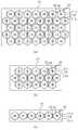
다수의 LED 패키지들은 도 1에 도시된 바와 같은 기판(1)에 일렬 또는 매트릭스 형태로 배열하여 LED 패키지 어레이(array)를 제조할 수 있다. 이때, LED 패키지(2)의 모양은 발광평면에서 원형, 사각형 등의 형태로 이루어져 있는데, 고 광도의 밝기를 내기 위해서 다수의 LED 패키지(2)가 배열에 적용되기도 한다.A plurality of LED packages may be arranged in a line or matrix form on the
그러나, 이러한 LED 패키지(2)는 그 모양이 원형이나 사각 형태로 되어 있기 때문에, 이를 개별적인 단품으로 사용하는 경우와는 달리 LED 패키지 어레이에 있어서는 LED 패키지(2)를 최대한 촘촘하게 배열할지라도 빈공간이 많이 생기게 된다. 즉, 도 1의 (b)에 도시된 바와 같은 LED 패키지 어레이에서는 원형의 기판(1)상에 사각형상의 LED 패키지(2) 배열시 사각형상의 LED 패키지 구조로 인해 빈공간 이 생기고, 사각형상의 LED 패키지(2)에서 실제 광이 나오는 면이 도 1의 (b)에서 보듯이 상기 LED 패키지의 하우징 면적보다 작기 때문에 더욱 빈공간이 많이 생기게 된다. 또한, 도 1의 (c)에 도시된 바와 같은 LED 패키지 어레이에서는 LED 패키지(1)로부터 리드가 외부로 길게 연장되어 있어, 다수의 LED 패키지(1) 배열시 빈공간이 많이 생기게 된다. 이러한 빈공간으로 인해 광손실이 크게 발생하며 전체 발광면에서도 광효율이 좋지 못하다. 특히, 도 1의 (a)에 도시된 바와 같은 LED 패키지 어레이에서는 다수의 LED 패키지(2)를 배열시, 기판(1)에 배열된 LED 패키지(2) 형상 자체가 비대칭이므로 전체 발광면의 균일성(Uniformity)이 좋지 않게 된다. 또한, 좌/우, 상/하 발광 패턴이 서로 다르다.However, since the
본 발명이 이루고자 하는 기술적 과제는, LED 패키지의 광손실을 줄이고 전체 발광면의 균일성을 향상시킬 수 있도록 하는 LED 패키지 어레이를 제공하는데 있다.An object of the present invention is to provide an LED package array that can reduce the light loss of the LED package and improve the uniformity of the entire light emitting surface.
상기 기술적 과제들을 이루기 위하여, 본 발명의 실시예에 따른 LED 패키지 어레이는 기판과, 상기 기판상에 배열되는 정육각형의 구조를 갖는 복수의 LED패키지로 이루어지되, 상기 복수의 LED 패키지는 LED칩 및 상기 LED칩을 수용하는 하우징을 포함하고, 상기 하우징은 상기 LED 칩에서 발생한 광의 방출이 이루어지는 정육각형의 상부면과, 상기 상부면과 수직을 이루는 6개의 측면들로 이루어지는 것을 특징으로 한다.In order to achieve the above technical problem, the LED package array according to an embodiment of the present invention comprises a substrate, a plurality of LED packages having a regular hexagonal structure arranged on the substrate, the plurality of LED packages are LED chip and the It includes a housing for accommodating the LED chip, the housing is characterized in that consisting of the upper surface of the regular hexagon that the light emitted from the LED chip is made, and six sides perpendicular to the upper surface.
본 실시예에 따라, 상기 복수의 LED 패키지 중 적어도 하나의 LED 패키지는 상기 6개의 측면들 중 적어도 하나의 측면이 이웃하는 다른 LED 패키지의 측면과 평행하게 마주한다. 또한, 상기 복수의 LED 패키지 중 하나의 LED 패키지는 상기 기판과 중심이 일치하도록 배치됨이 바람직하다. 더욱 바람직하게 상기 하나의 LED 패키지는 상기 6개의 측면 모두가 이웃하는 다른 LED 패키지의 측면과 평행하게 마주할 수 있다. 또한, 상기 복수의 LED 패키지 중 하나의 LED 패키지는 서로 이웃하는 측면들에 리드프레임들 각각을 구비하며, 상기 리드프레임들은 상기 기판상의 한 솔더링 패턴에 함께 연결될 수 있다. 이때, 상기 기판은 원형을 포함한다.According to this embodiment, at least one LED package of the plurality of LED packages faces in parallel with a side of another LED package in which at least one side of the six sides is adjacent. In addition, it is preferable that one LED package of the plurality of LED packages is arranged to coincide with the substrate. More preferably the one LED package may face the six sides in parallel with the side of another neighboring LED package. In addition, one LED package of the plurality of LED packages includes each of the lead frames on side surfaces adjacent to each other, and the lead frames may be connected together in one soldering pattern on the substrate. In this case, the substrate includes a circle.
더 나아가, 상기 LED 패키지는 LED칩 및 상기 LED칩을 수용하는 하우징을 갖되, 상기 하우징은 상기 LED칩에서 발생한 광의 방출이 이루어지는 정육각형의 상부면; 및 상기 상부면과 수직을 이루는 6개의 측면들을 포함한다. 여기에서, 상기 LED칩은 상기 하우징에 지지되는 복수의 리드프레임으로부터 전류를 인가받되, 상기 리드프레임들 각각은 상기 6개의 측면들 중 하나의 측면을 관통하여 연장된 것을 특징으로 한다.Furthermore, the LED package has a housing for accommodating the LED chip and the LED chip, the housing is a top surface of the regular hexagon is made to emit light generated from the LED chip; And six side surfaces perpendicular to the upper surface. Herein, the LED chip receives current from a plurality of lead frames supported by the housing, wherein each of the lead frames extends through one side of the six sides.
이하, 첨부한 도면들을 참조하여 본 발명의 실시예들을 상세히 설명하기로 한다. 다음에 소개되는 실시예들은 당업자에게 본 발명의 사상이 충분히 전달될 수 있도록 하기 위해 예로서 제공되는 것이다. 따라서, 본 발명은 이하 설명되는 실시예들에 한정되지 않고 다른 형태로 구체화될 수도 있다. 그리고, 도면들에 있어서, 구성요소의 폭, 길이, 두께 등은 편의를 위하여 과장되어 표현될 수 있다. 명세서 전체에 걸쳐서 동일한 참조번호들은 동일한 구성요소들을 나타낸다.Hereinafter, embodiments of the present invention will be described in detail with reference to the accompanying drawings. The following embodiments are provided as examples to ensure that the spirit of the present invention can be fully conveyed to those skilled in the art. Accordingly, the present invention is not limited to the embodiments described below and may be embodied in other forms. And, in the drawings, the width, length, thickness, etc. of the components may be exaggerated for convenience. Like numbers refer to like elements throughout.
도 2 는 본 발명의 실시예에 따른 LED 패키지의 평면도이고, 도 3 은 도 2의 X-X를 따라 취해진 단면도이며, 도 4 는 도 2에 도시된 LED 패키지의 저면도이다.FIG. 2 is a plan view of the LED package according to the embodiment of the present invention, FIG. 3 is a sectional view taken along X-X of FIG. 2, and FIG. 4 is a bottom view of the LED package shown in FIG.
도 2 내지 도 4에 도시된 바와 같이 본 실시예에 따른 LED 패키지(20)는 대칭형태로, 전체적인 외형은 정육각형의 구조를 갖는다. 이 LED 패키지(20)는 리드프레임으로 형성되어 외부 전극들에 연결되는 제 1 및 제 2 리드프레임(22, 24) 및 이들과 일체로 성형된 하우징(21)을 구비한다. 이러한 하우징(21)은 폴리프탈아미드(Polyphthalamide; PPA)일 수 있으며, LED 패키지 내부 구조를 다양하게 설계할 수 있다. 상기 제 1 및 제 2 리드프레임(22, 24)은 각각의 일단이 근접하여 대향하도록 배치되며, 타단은 서로 반대방향으로 연장되어 하우징(21)의 외부로 돌출된다.2 to 4, the
상기 하우징(21)은 LED칩(26)을 수용한 채 상기 LED칩(26)에서 발생한 광의 방출이 이루어지는 정육각형의 상부면(21a)과, 그 상부면(21a)과 수직을 이루는 6개의 측면(21b)들로 이루어진다. 여기에서, 상기 LED칩(26)은 상기 하우징(21)에 지지되는 제 1 및 제 2 리드프레임(22, 24)으로부터 전류를 인가받는다. 이 제 1 및 제 2 리드프레임들(22, 24) 각각은 6개의 측면(21b) 중 하나의 측면(21b)을 관통하여 연장되되, 그 연장된 부분에서 상기 제 1 및 제 2 리드프레임들(22, 24)들의 측면은 하우징(21)의 측면과 평행하게 그리고 하우징(21)의 하부면을 향해 절곡되 구조를 이룬다. 상기 절곡에 의해 하우징(21)의 측면과 평행하게 되는 제 1 및 제 2 리드프레임(22, 24)의 일부는 상기 하우징(21)의 측면과 가깝게 근접하여 있는 것이 바람직하다.The
도면에서는 하우징(21)의 서로 마주하는 한 쌍의 측면들에 한 쌍의 리드프레임(22, 24)이 도시되어 있지만, 다른 측면들에도 리드프레임들이 마련될 수 있다. 이 경우, LED 패키지들을 직렬, 병렬 또는 직병렬 등으로 다양하게 연결할 수 있으며, 각 패키지 내에 복수개의 LED칩들을 실장하여 각 패키지 내의 LED칩들을 개별구동할 수도 있다.In the figure, a pair of
이와 같은 정육각형의 하우징(21)은 제 1 및 제 2 리드프레임(22, 24)을 노출시키는 오목부(25)를 갖는다. 상기 오목부(25)의 바닥면에는 상기 LED칩(26)이 실장된다. 이때, 상기 LED칩(26)은 제 1 리드프레임(22) 상에 도전성 접착제에 의해 부착될 수 있다. 이에 더하여, 상기 LED칩(26)은 본딩와이어(W)를 통해 제 2 리드프레임(24)에 접속될 수 있다. 이에 따라, 상기 LED칩(26)은 제 1 및 제 2 리드프레임(22, 24)에 전기적으로 연결된다.Such a regular
한편, 상기 오목부(25)에는 에폭시 또는 실리콘과 같은 투광성 수지의 봉지부재(27)가 채워진다. 상기 봉지부재(27)는 오목부(25)의 바닥면에 실장된 상기 LED칩(26) 상부 및 본딩와이어(W)를 덮음으로써 LED 패키지를 형성한다.On the other hand, the
여기에서, 봉지부재(27)의 상부면은 도면에 도시된 바와 같이 평평한 면일 수도 있으며, 일정한 곡률을 가질 수도 있다. 또한, 봉지부재(27)는 적어도 하나의 형광체를 함유할 수도 있다. 이에 따라, 상기 LED칩(26)으로부터 나온 광을 형광체에 의해 색변환시켜 다양한 색을 만들 수 있다.Here, the upper surface of the sealing
도 5를 참조하여 본 발명의 실시예에 따른 LED 패키지 어레이를 설명하면 다음과 같다.The LED package array according to the embodiment of the present invention will be described with reference to FIG. 5.
도 5는 본 발명의 실시예에 따른 LED 패키지 어레이를 설명하기 위한 도면이다.5 is a view for explaining an LED package array according to an embodiment of the present invention.
도 5에 도시된 바와 같이 본 실시예에 따른 LED 패키지 어레이는 크게 전기신호를 전달하기 위한 도전성패턴이 형성되는 기판(10)과, 그 기판(10)에 배열된 채 광을 발산하는 복수의 LED 패키지(20)로 이루어진다. 이때, 기판(10)상에 배열되는 복수의 LED 패키지(20)는 앞에서 설명하였으므로, 그 상세한 설명을 생략한다.As shown in FIG. 5, the LED package array according to the present embodiment includes a
이 LED 패키지(20)는 마치 벌집의 모양처럼 복수개가 일정간격으로 기판(10)에 배열될 수 있다. 또한, 기판(10)에는 높은 광출력을 위해 적어도 2개의 LED칩(26)이 실장된 복수의 LED 패키지(20)가 배열될 수 있다.The
본 실시예에 따라, 상기 기판(10)은 원형 혹은 환형일 수 있으나, 본 발명이 이에 한정되는 것은 아니다. 또한, 상기 기판(10)은 인쇄회로기판(PCB: Printed Circuit Board)일 수 있으며, 상기 기판(10)에는 복수의 LED 패키지(20)에 전원을 공급하기 위한 리드단자(미도시)들이 서로 이격되게 배치되고, 그 리드단자들은 기판(10)상에 배열된 LED 패키지(20)에 설치된 제 1 및 제 2 리드프레임(22, 24)과 전기적으로 접속되어 있다. 이 리드단자는 예를 들면, 구리 박막과 같은 전도성 박막 금속을 도금, 프린팅, 또는 기타 다른 방식을 통해 형성하여 이루어지는 것이다.According to the present embodiment, the
한편, 상기 복수의 LED 패키지(20)의 각각은 6개의 측면(21b)들을 포함하는 정육각형 구조로 이루어지고, 상기 6개의 측면(21b) 중 적어도 하나의 측면(21b)은 이웃하는 다른 패키지의 측면과 평행하게 마주한다. 이는 도 5에 잘 도시되어 있다. 이때, 복수개의 LED 패키지(20)는 각각의 LED 패키지(20)에서 나온 광의 출력을 극대화시킬 수 있을 정도의 간격을 두고 기판에 배열하는 것이 바람직하다.Meanwhile, each of the plurality of LED packages 20 has a regular hexagonal structure including six
또한, 상기 복수의 LED 패키지(20) 중 하나의 LED 패키지(a)는 상기 기판(10)과 중심이 일치하도록 배치된다. 그 하나의 LED 패키지(a)는 6개의 측면(21b) 모두가 이웃하는 다른 LED 패키지의 측면과 평행하게 마주한다.In addition, one LED package (a) of the plurality of
또한, 상기 하나의 LED 패키지(a)와 평행하게 마주한 채 일정간격을 두고 하나의 LED 패키지(a)를 둘러싸게 복수의 LED 패키지(20)들이 기판(10)에 배열될 수 있다. 이에 따라, LED 패키지(20)간의 틈새를 줄일 수 있어, 동일한 수량과 크기 대비 광효율을 극대화시킬 수 있다.In addition, a plurality of
이와 같이 기판(10)상에 복수의 LED 패키지(20)가 배열된 LED 패키지 어레이는 조명이나 등 기구, 자동차 헤드램프(Head Lamp) 등에 적합하다.The LED package array in which the plurality of
도 6은 본 발명이 적용되는 정육각형 구조를 갖는 LED 패키지의 적용예를 도시한 도면으로, 도 6의 (a)는 본 발명의 LED 패키지가 일렬로 배열될 때의 평면도를 나타내고, 도 6의 (b)는 LED 패키지가 일렬로 배열될 때의 저면도를 나타내며, 도 6의 (c)는 일렬로 배열된 LED 패키지의 회로도를 나타낸다.6 is a view showing an application example of the LED package having a regular hexagonal structure to which the present invention is applied, Figure 6 (a) shows a plan view when the LED package of the present invention is arranged in a line, b) shows a bottom view when the LED packages are arranged in a line, and FIG. 6C shows a circuit diagram of the LED packages arranged in a line.
정육각형의 구조로 이루어진 복수의 LED 패키지(20)를 기판(10)에 배열시, 도 6의 (b)에서 보는 바와 같이 복수의 LED 패키지(20)들 중 하나의 LED 패키지가 서로 이웃하는 측면들에 리드프레임들(22, 24) 각각을 구비하며, 상기 리드프레임들(22, 24)은 상기 기판(10)상의 한 솔더링(soldering) 패턴(b)에 함께 연결될 수 있다. 서로 이웃하는 측면들에 구비된 채 평행하게 마주하는 리드프레임들(22, 24)을 기판(10)상의 한 솔더링 패턴에 연결하기 위하여 예를 들면, 리플로우 솔더링 공정과 같은 SMT(Surface Mount Technology)를 이용할 수 있다. 이에 따라, 최소 공간에 최대한 밀착하여 복수의 LED 패키지(20)를 연결할 수 있어 LED 패키지(20)간의 집결성이 우수하며, 전체적으로 광효율을 높일 수 있다. 또한, 시준기(collimator) 장착에도 용이하여 광출력을 극대화시킬 수 있다.When arranging a plurality of
도 7은 본 발명이 적용되는 다른 실시예의 LED 패키지 어레이를 설명하기 위한 도면이다.7 is a view for explaining an LED package array of another embodiment to which the present invention is applied.
도 7에 도시된 바와 같은 LED 패키지 어레이는 사각형의 기판(10)과, 그 기판(10)에 배열되는 복수개의 LED 패키지(20)로 이루어진다. 이러한 LED 패키지 어레이는 직교형 배열형태로, 소/중/대형 LCD 백라이트와 다출력 면적의 면 발광을 필요로 하는 제품에 적용될 수 있다.The array of LED packages as shown in FIG. 7 consists of a
제품 적용에 따라 기판(10)에는 적어도 하나의 열로 복수의 LED 패키지(20)를 배열할 수 있다. 즉, 도 7의 (a)에서 보는 바와 같이 5열로 복수의 LED 패키지(20)를 기판(10)에 배열할 수도 있고, 도 7의 (b)에서 보는 바와 같이 3열로 복수의 LED 패키지(20)를 기판(10)에 배열할 수도 있으며, 도 7의 (c)에서 보는 바와 같이 1열로 복수의 LED 패키지(20)를 기판(10)에 배열할 수도 있다. 이때, 기판(10)에 배열되는 복수의 LED 패키지(20)의 개수는 제품에 발광면에 따라 다르게 적용될 수 있다.According to a product application, the plurality of
본 발명의 실시예에 따르면 기판상에 배열된 정육각형 구조를 갖는 복수의 LED 패키지가 서로 이웃하는 다른 패키지와 적어도 하나의 측면을 평행하게 마주함으로써 복수의 LED 패키지 간의 틈새를 최소화하고 LED 패키지의 밀집성을 높일 수 있다. 이에 따라, LED 패키지의 배열시 빈공간으로 인한 광 손실을 줄일 수 있으며, 평면상 거의 모든 방향으로 발광의 패턴을 갖게 함으로써 발광면의 균일성을 높여 광효율을 향상시킬 수 있다.According to an embodiment of the present invention, a plurality of LED packages having a regular hexagonal structure arranged on a substrate face at least one side surface in parallel with other neighboring packages in parallel, thereby minimizing gaps between the plurality of LED packages and increasing density of the LED packages. It can increase. Accordingly, it is possible to reduce the light loss due to the empty space when arranging the LED package, and to improve the light efficiency by increasing the uniformity of the light emitting surface by having a light emission pattern in almost all directions on the plane.
또한, 본 발명의 실시예에 따르면 상기 복수의 LED 패키지 중 하나의 LED 패키지를 기판의 중심과 일치하도록 배치하고, 하나의 LED 패키지의 측면 모두가 다른 LED 패키지의 측면과 평행하게 마주함으로써, 복수의 LED 패키지 배열시 LED 패키지간의 광 출력 사각지대를 최소화하여 광 손실을 줄일 수 있다.In addition, according to an embodiment of the present invention by placing one LED package of the plurality of LED packages to match the center of the substrate, all of the sides of one LED package facing in parallel with the side of the other LED package, When the LED package is arranged, light loss can be reduced by minimizing the blind spot between the LED packages.
그리고, 본 발명의 실시예에 따르면 복수의 LED 패키들 중 서로 이웃하는 측면들에 리드프레임들을 상기 기판상에 한 솔더링 패턴에 함께 연결함으로써 솔더링 패턴수를 줄일 수 있고, 그로 인해 솔더링 패턴에 사용되는 금속재료량을 줄일 수 있으며, 기판상에 솔더링 패턴을 단순화시킬 수 있다.According to an embodiment of the present invention, the number of soldering patterns can be reduced by connecting leadframes together on one side of the plurality of LED packages to one soldering pattern on the substrate, thereby reducing the number of soldering patterns. The amount of metal material can be reduced, and the soldering pattern on the substrate can be simplified.
Claims (8)
Translated fromKoreanPriority Applications (1)
| Application Number | Priority Date | Filing Date | Title |
|---|---|---|---|
| KR20070065358AKR20090001169A (en) | 2007-06-29 | 2007-06-29 | LED packages and arrays thereof |
Applications Claiming Priority (1)
| Application Number | Priority Date | Filing Date | Title |
|---|---|---|---|
| KR20070065358AKR20090001169A (en) | 2007-06-29 | 2007-06-29 | LED packages and arrays thereof |
Publications (1)
| Publication Number | Publication Date |
|---|---|
| KR20090001169Atrue KR20090001169A (en) | 2009-01-08 |
Family
ID=40484275
Family Applications (1)
| Application Number | Title | Priority Date | Filing Date |
|---|---|---|---|
| KR20070065358AWithdrawnKR20090001169A (en) | 2007-06-29 | 2007-06-29 | LED packages and arrays thereof |
Country Status (1)
| Country | Link |
|---|---|
| KR (1) | KR20090001169A (en) |
Cited By (2)
| Publication number | Priority date | Publication date | Assignee | Title |
|---|---|---|---|---|
| KR101399997B1 (en)* | 2012-10-25 | 2014-05-30 | 한국광기술원 | Led package with hexagonal structure |
| WO2017217576A1 (en)* | 2016-06-16 | 2017-12-21 | 주식회사 올릭스 | Led package |
- 2007
- 2007-06-29KRKR20070065358Apatent/KR20090001169A/ennot_activeWithdrawn
Cited By (2)
| Publication number | Priority date | Publication date | Assignee | Title |
|---|---|---|---|---|
| KR101399997B1 (en)* | 2012-10-25 | 2014-05-30 | 한국광기술원 | Led package with hexagonal structure |
| WO2017217576A1 (en)* | 2016-06-16 | 2017-12-21 | 주식회사 올릭스 | Led package |
Similar Documents
| Publication | Publication Date | Title |
|---|---|---|
| TWI467737B (en) | Light-emitting diode package structure, illumination device, and substrate for LED package | |
| EP2187459B1 (en) | Light emitting device | |
| US9146026B2 (en) | Lighting device including light-emitting element and method for manufacturing the same | |
| JP5197874B2 (en) | Light emitting module, light source device, liquid crystal display device, and method for manufacturing light emitting module | |
| US8338851B2 (en) | Multi-layer LED array engine | |
| CN1945822B (en) | Semiconductor device, semiconductor module and semiconductor module producing method | |
| CN101930972B (en) | LED device | |
| KR101662038B1 (en) | Chip package | |
| CN103430339B (en) | Substrate, light-emitting device, and illumination device | |
| KR101584726B1 (en) | Emitting module | |
| JP2011243935A (en) | Light-emitting device and lighting device | |
| JP2006295085A (en) | Light-emitting diode light source unit | |
| KR20110121927A (en) | Lighting device using light emitting device package | |
| JP2012004391A (en) | Light-emitting device and luminaire | |
| US20120241773A1 (en) | Led bar module with good heat dissipation efficiency | |
| CN102214776B (en) | Light emitting diode package, lighting device and light emitting diode package substrate | |
| US8138517B2 (en) | Light-emitting diode package | |
| US8247821B2 (en) | Pre-molded support mount of lead frame-type for LED light module | |
| CN210956669U (en) | COB light source of mirror surface aluminum substrate | |
| JP2006344564A (en) | LED light source unit | |
| KR20090001169A (en) | LED packages and arrays thereof | |
| JP5769129B2 (en) | Light emitting device and lighting device | |
| KR20140064582A (en) | Side light emitting led package, lighting array module, and fabrication method therof | |
| KR101201558B1 (en) | LED package | |
| KR101255747B1 (en) | Light emitting device module and lightening apparatus therewith |
Legal Events
| Date | Code | Title | Description |
|---|---|---|---|
| PA0109 | Patent application | Patent event code:PA01091R01D Comment text:Patent Application Patent event date:20070629 | |
| PG1501 | Laying open of application | ||
| PC1203 | Withdrawal of no request for examination | ||
| WITN | Application deemed withdrawn, e.g. because no request for examination was filed or no examination fee was paid |