KR20080098412A - RFID tag, manufacturing method of RFID tag and RFID tag installation method - Google Patents
RFID tag, manufacturing method of RFID tag and RFID tag installation methodDownload PDFInfo
- Publication number
- KR20080098412A KR20080098412AKR1020087021646AKR20087021646AKR20080098412AKR 20080098412 AKR20080098412 AKR 20080098412AKR 1020087021646 AKR1020087021646 AKR 1020087021646AKR 20087021646 AKR20087021646 AKR 20087021646AKR 20080098412 AKR20080098412 AKR 20080098412A
- Authority
- KR
- South Korea
- Prior art keywords
- slot
- dielectric substrate
- rfid tag
- chip
- conductor pattern
- Prior art date
- Legal status (The legal status is an assumption and is not a legal conclusion. Google has not performed a legal analysis and makes no representation as to the accuracy of the status listed.)
- Abandoned
Links
Images


Classifications
- G—PHYSICS
- G06—COMPUTING OR CALCULATING; COUNTING
- G06K—GRAPHICAL DATA READING; PRESENTATION OF DATA; RECORD CARRIERS; HANDLING RECORD CARRIERS
- G06K19/00—Record carriers for use with machines and with at least a part designed to carry digital markings
- G06K19/06—Record carriers for use with machines and with at least a part designed to carry digital markings characterised by the kind of the digital marking, e.g. shape, nature, code
- G06K19/067—Record carriers with conductive marks, printed circuits or semiconductor circuit elements, e.g. credit or identity cards also with resonating or responding marks without active components
- G06K19/07—Record carriers with conductive marks, printed circuits or semiconductor circuit elements, e.g. credit or identity cards also with resonating or responding marks without active components with integrated circuit chips
- G06K19/077—Constructional details, e.g. mounting of circuits in the carrier
- G06K19/07749—Constructional details, e.g. mounting of circuits in the carrier the record carrier being capable of non-contact communication, e.g. constructional details of the antenna of a non-contact smart card
- G—PHYSICS
- G06—COMPUTING OR CALCULATING; COUNTING
- G06K—GRAPHICAL DATA READING; PRESENTATION OF DATA; RECORD CARRIERS; HANDLING RECORD CARRIERS
- G06K19/00—Record carriers for use with machines and with at least a part designed to carry digital markings
- G06K19/06—Record carriers for use with machines and with at least a part designed to carry digital markings characterised by the kind of the digital marking, e.g. shape, nature, code
- G06K19/067—Record carriers with conductive marks, printed circuits or semiconductor circuit elements, e.g. credit or identity cards also with resonating or responding marks without active components
- G06K19/07—Record carriers with conductive marks, printed circuits or semiconductor circuit elements, e.g. credit or identity cards also with resonating or responding marks without active components with integrated circuit chips
- G06K19/077—Constructional details, e.g. mounting of circuits in the carrier
- G06K19/07749—Constructional details, e.g. mounting of circuits in the carrier the record carrier being capable of non-contact communication, e.g. constructional details of the antenna of a non-contact smart card
- G06K19/07771—Constructional details, e.g. mounting of circuits in the carrier the record carrier being capable of non-contact communication, e.g. constructional details of the antenna of a non-contact smart card the record carrier comprising means for minimising adverse effects on the data communication capability of the record carrier, e.g. minimising Eddy currents induced in a proximate metal or otherwise electromagnetically interfering object
- H—ELECTRICITY
- H01—ELECTRIC ELEMENTS
- H01Q—ANTENNAS, i.e. RADIO AERIALS
- H01Q1/00—Details of, or arrangements associated with, antennas
- H01Q1/12—Supports; Mounting means
- H01Q1/22—Supports; Mounting means by structural association with other equipment or articles
- H01Q1/2208—Supports; Mounting means by structural association with other equipment or articles associated with components used in interrogation type services, i.e. in systems for information exchange between an interrogator/reader and a tag/transponder, e.g. in Radio Frequency Identification [RFID] systems
- H01Q1/2225—Supports; Mounting means by structural association with other equipment or articles associated with components used in interrogation type services, i.e. in systems for information exchange between an interrogator/reader and a tag/transponder, e.g. in Radio Frequency Identification [RFID] systems used in active tags, i.e. provided with its own power source or in passive tags, i.e. deriving power from RF signal
- H—ELECTRICITY
- H01—ELECTRIC ELEMENTS
- H01Q—ANTENNAS, i.e. RADIO AERIALS
- H01Q1/00—Details of, or arrangements associated with, antennas
- H01Q1/12—Supports; Mounting means
- H01Q1/22—Supports; Mounting means by structural association with other equipment or articles
- H01Q1/24—Supports; Mounting means by structural association with other equipment or articles with receiving set
- H—ELECTRICITY
- H01—ELECTRIC ELEMENTS
- H01Q—ANTENNAS, i.e. RADIO AERIALS
- H01Q1/00—Details of, or arrangements associated with, antennas
- H01Q1/36—Structural form of radiating elements, e.g. cone, spiral, umbrella; Particular materials used therewith
- H01Q1/38—Structural form of radiating elements, e.g. cone, spiral, umbrella; Particular materials used therewith formed by a conductive layer on an insulating support
- H—ELECTRICITY
- H01—ELECTRIC ELEMENTS
- H01Q—ANTENNAS, i.e. RADIO AERIALS
- H01Q13/00—Waveguide horns or mouths; Slot antennas; Leaky-waveguide antennas; Equivalent structures causing radiation along the transmission path of a guided wave
- H01Q13/10—Resonant slot antennas
Landscapes
- Engineering & Computer Science (AREA)
- Physics & Mathematics (AREA)
- Computer Hardware Design (AREA)
- Microelectronics & Electronic Packaging (AREA)
- General Physics & Mathematics (AREA)
- Theoretical Computer Science (AREA)
- Electromagnetism (AREA)
- Details Of Aerials (AREA)
- Waveguide Aerials (AREA)
Abstract
Translated fromKoreanDescription
Translated fromKorean본 발명은, Radio Frequency Identification(이하, RFID라 칭한다)리더 라이터로부터 송신되는 코맨드 신호를 RFID태그가 수신하고, 그 코맨드 신호의 정보에 따라 RFID태그내의 메모리에 격납되어 있는 태그 정보의 갱신·기록, 또는 그 태그 정보를 RFID태그가 RFID리더 라이터에 판독신호로서 송신하고, 생체·물품의 입퇴실 관리나 물류관리 등에 이용되는 UHF대 및 마이크로파대의 RFID시스템의 RFID 태그 및 그 제조 방법, 및 그 설치 방법에 관한 것이다.According to the present invention, an RFID tag receives a command signal transmitted from a Radio Frequency Identification (hereinafter, referred to as RFID) reader / writer, and updates and records tag information stored in a memory in the RFID tag according to the information of the command signal. Or an RFID tag of a UHF band and a microwave band RFID system used for transmitting and receiving tag information as a read signal to an RFID reader / writer and used for logistic management of living rooms and articles, and a method of manufacturing the same It is about.
RFID시스템은, IC칩을 구비한 RFID태그와 RFID리더 라이터와의 사이에서 무선통신을 행하는 시스템이다. RFID 태그에는, 배터리를 탑재하고, 그 전력으로 구동하는 액티브형 태그와, 리더 라이터로부터의 전력을 받고, 이것을 전원으로 하여 구동하는 패시브형 태그가 있다. 액티브형은 패시브형에 비교하여, 배터리를 탑재하고 있기 때문에, 통신 거리, 통신의 안정도등의 장점이 있는 반면, 구조의 복잡화, 사이즈의 대형화, 고비용 등의 결점도 있다. 또한, 최근의 반도체기술의 향상에 의해, 패시브형 태그용 IC칩의 소형화, 고성능화가 진행하고, 패시브형 태그의 폭넓은 분야에서의 사용이 기대되고 있다. 패시브형 태그에 있어서, 주파수대가 장파대, 단파대의 RFID태그에서 적용되어 있는 전자유도방식에서는, 리더 라이터의 송신안테나 코일과 RFID태그의 안테나 코일과의 사이의 전자유도작용으로 RFID태그에 전압이 유기되고, 이 전압에 의해 IC칩을 기동해서 통신을 가능하게 하고 있다. 따라서, RFID리더 라이터에 의한 유도 전자계내에서만 RFID태그가 동작하지 않고, 통신 거리는 수십cm정도가 되어 버린다.The RFID system is a system for performing wireless communication between an RFID tag having an IC chip and an RFID reader / writer. The RFID tag includes an active tag that has a battery mounted thereon and is driven by the power, and a passive tag that receives power from the reader / writer and drives the power as the power source. Compared with the passive type, since the active type has a battery, the active type has advantages such as communication distance and communication stability, but also has disadvantages such as complicated structure, large size, and high cost. In addition, with the recent improvement in semiconductor technology, the miniaturization and high performance of the passive tag IC chip has progressed, and the use of the passive tag in a wide field is expected. In the passive tag, in the electromagnetic induction method in which the frequency band is applied to the RFID tag of the long wave band and the short wave band, voltage is induced to the RFID tag by the electromagnetic induction action between the transmitting antenna coil of the reader / writer and the antenna coil of the RFID tag. With this voltage, the IC chip is activated to enable communication. Therefore, the RFID tag does not operate only in the induction electromagnetic field by the RFID reader / writer, and the communication distance becomes about several tens of centimeters.
또한, UHF대 및 마이크로파대 등의 높은 주파수대의 RFID태그에서는, 전파통신방식이 적용되어 있고, 전파에 의해 RFID태그의 IC칩에 전력을 공급하고 있기 때문에, 통신 거리는 1∼8m정도로 대폭 향상하고 있다. 따라서, 통신 거리의 짧은 장파대, 단파대의 RFID시스템에서는 실현이 곤란했던 복수매의 RFID태그의 일괄 판독이나 이동하고 있는 RFID태그의 판독 등이 가능해지고, 그 이용 범위는, 대폭 확대된다고 생각된다. UHF대 및 마이크로파대 등의 높은 주파수의 패시브형 태그로서, 예를 들면 특허문헌1이나 특허문헌2 등에 개시되어 있다.In the high frequency RFID tags such as the UHF band and the microwave band, the radio wave communication method is applied, and since the electric power is supplied to the IC chip of the RFID tag by radio waves, the communication distance is greatly improved to about 1 to 8 m. . Therefore, it is possible to collectively read a plurality of RFID tags, to read moving RFID tags, and the like, which are difficult to realize in an RFID system of short-wavelength or short-wavelength communication distance, and the use range is considered to be greatly expanded. As high frequency passive tags, such as a UHF band and a microwave band, it is disclosed by
종래, RFID태그의 기술에서는, 특허문헌1의 제12도(66은 다이폴안테나, 67은 IC 칩)에 도시된 다이폴안테나(66)에 IC칩(67)을 설치 함에 의해, RFID 시스템의 태그로서 동작하는 것이나, 특허문헌2의 제2도(13은 1/2파장마이크로스트립선로 공진기, 14는 유전체 기판, 15는 접지 도체판)에 도시된 1/2파장 마이크로스트립선로 공진기(13)와 접지 도체판(15)과의 사이에 IC칩을 접속함으로써, 접지 도체판(15)측에 금속물체(도체)가 있어도 안테나의 방사특성에는, 대부분 영향을 주지 않고 금속물체(도체)에 설치나 접착이 가능한 것이 있다.Conventionally, in the technology of the RFID tag, the IC chip 67 is provided in the dipole antenna 66 shown in FIG. 12 (66 is a dipole antenna and 67 is an IC chip) of
또한, 특허문헌3의 제1도에는, 기본재료(1)의 표면에 형성된 단자부(3), 기본재료(1)의 일부에 형성된 IC칩 배치 영역(9)에 배치되고, 단자부(3)에 접속된 IC칩(6)을 구비한 RFID태그가 개시되어 있다.Moreover, in FIG. 1 of
그리고, 거기에는, IC칩(6)을 기본재료(1)의 내부에 매립할 필요는 없고, 안테나 윗면에 설치할 수 있기 때문에, 기본재료(1)의 표면에 대한 가공만으로 간편한 구조의 RFID태그를 제조할 수 있고, 수율의 저감·제조 코스트 다운이 가능하게 된다고 하는 것이 개시되어 있다.In addition, since the
한층 더, 특허문헌4의 제19도에는, 유전체부재(10), IC칩용 오목부(10b), 필름 기본재료(20), 안테나 패턴(30), IC칩(40)을 구비한 RFID태그(5)이며, 유전체부재(10)에 IC칩(40)을 매설가능한 IC칩용 오목부(10b)를 설치하고, 이 IC칩용 오목부(10b)에 IC칩(40)을 매설시켜, 필름 기본재료(20)의 내면측에 형성한 안테나 패턴(30)과 IC칩(40)이 전기적으로 접속하도록 필름 기본재료(20)를 유전체부재(10)에 둘러 감아서 안테나 패턴(30)에 의해 구성한 루프 안테나에 의해, 전파흡수체의 근방에서도 통신 거리의 저하를 억제한 것이 개시되어 있다.Furthermore, in Fig. 19 of
또한, 특허문헌5의 제4도에는, 안테나면(30)에 있어서, 유전체(20)의 일부를 노출시키는 개구(31)가 형성되어 있는 것이 기재되어 있다.Moreover, in FIG. 4 of
개구는, 서로 대향하도록 평행하게 연장되는 한 쌍의 제1슬릿(31a)과, 상기 한 쌍의 슬릿(31a)과, 상기 한 쌍의 슬릿(31a)을 연통하는 제2슬릿(31b)을 갖고, 상기 제2슬릿(31b)을 상기 한 쌍의 제1슬릿(31a)의 중간부에 위치시킨 RFID태그가 개시되어 있다. 이때, 송수신소자(IC칩)는, 제1 및 제2급전점은 41, 42에 접속되어 있다.The opening has a pair of first slits 31a extending in parallel to face each other, a pair of slits 31a, and a second slit 31b communicating with the pair of slits 31a. An RFID tag in which the second slit 31b is positioned at an intermediate portion of the pair of first slits 31a is disclosed. At this time, the first and second feed points of the transmission / reception element (IC chip) are connected to 41 and 42.
특허문헌1: 일본국 공개특허공보 특개2003-249820호(제12도)Patent Document 1: Japanese Patent Application Laid-Open No. 2003-249820 (Fig. 12)
특허문헌2: 일본국 공개특허공보 특개2000-332523호(제3도)Patent Document 2: Japanese Patent Application Laid-Open No. 2000-332523 (FIG. 3)
특허문헌3: 일본국 공개특허공보 특개2002-197434호(제1도)Patent Document 3: Japanese Laid-Open Patent Publication No. 2002-197434 (Fig. 1)
특허문헌4: 일본국 공개특허공보 특개2006-53833호(제19도)Patent Document 4: Japanese Laid-Open Patent Publication No. 2006-53833 (Fig. 19)
특허문헌5: 일본국 공개특허공보 특개2006-237674호(제4도)Patent Document 5: Japanese Laid-Open Patent Publication No. 2006-237674 (Fig. 4)
종래의 RFID태그(특허문헌1에 개시되어 있는 RFID태그)는 이상과 같이 구성되어 있으므로, 금속물체 등의 도전성 물체(도체)에 접착하거나, 그 근방에 설치할 경우, 도전성 물체의 영향으로 다이폴안테나(1)가 동작하지 않게 되거나, 통신거리가 극단적으로 저하해버리는 등의 과제가 있었다.Since a conventional RFID tag (RFID tag disclosed in Patent Document 1) is constituted as described above, when affixed to or attached to a conductive object (conductor) such as a metal object or installed in the vicinity thereof, a dipole antenna ( There were problems such as 1) not working or extremely short communication distance.
특허문헌2에 개시되어 있는 RFID태그에서는, 금속물체(도체)에 설치하는 것은 가능하지만, 1/2파장 마이크로스트립선로 공진기와 접지 도체판과의 사이에 IC칩을 접속하는 구조이며, 유전체 기판 내부에 IC칩을 매립할 필요가 있기 위해서, 구조가 복잡해 제조가 곤란해져, 제조 비용의 증대를 초래하는 등의 과제가 있었다.The RFID tag disclosed in
또한, 특허문헌3에 개시되어 있는 RFID태그에서는, IC칩의 소형화가 진행하고 있어도, IC칩의 두께는 안테나 패턴이나 단자부의 도체 두께와 비교하면 두껍고, 게다가 IC칩이 기본재료의 표면에 설치되기 위해서 RFID태그의 표면에 돌기가 생겨버린다. 따라서, 특허문헌3의 [0023]항에 기재되는 것처럼, IC칩의 설치부 전체 혹은 일부를 피복 보호해서 RFID태그의 표면을 평탄하게 할 필요가 있다. 즉, 기본재료에 안테나 패턴 및 IC칩을 설치할 경우에는, 충격 등에 의해 IC칩이 파손할 우려가 있어, RFID 태그의 표면(윗면)에 라벨 프린터를 사용해 직접 인쇄하는 것이 어렵게 된다고 하는 과제가 있었다.In addition, in the RFID tag disclosed in
또한, 기본재료에 안테나 패턴과 IC칩을 설치한 필름을 접착할 경우에는, IC 칩에 의한 필름의 팽창(돌기)이 생기기 때문에, 역시 상기한 바와 같은 과제가 있었다.In addition, when the film provided with the antenna pattern and the IC chip is adhered to the base material, since the expansion (projection) of the film by the IC chip occurs, there has been the same problem as described above.
한층 더, 특허문헌4에 개시되어 있는 RFID태그에서는, IC칩에 의한 필름(필름 기본재료)의 팽창(돌기)이 거의 생기지 않지만, 금속물체 등의 도전성 물체(도체)에 접착하거나, 그 근방에 설치하거나 할 경우에는, 도전성 물체의 영향에 의해 루프안테나가 동작하지 않게 되거나, 통신 거리가 극단적으로 저하해버린다고 하는 과제가 있었다.Furthermore, in the RFID tag disclosed in
또한, 특허문헌5에 개시되어 있는 RFID태그에서는, 개구가 서로 대향하도록 평행하게 연장되는 한 쌍의 제1슬릿(31a)과, 상기 한 쌍의 슬릿(31a)과, 상기 한 쌍의 슬릿(31a)을 연통하는 제2슬릿(31b)을 갖고, 상기 개구(31)는, 안테나면(30) 중 상기 개구(31)를 통해서 노출하는 유전체(20)에 의해 구획되는 영역(36, 37)이 송수신소자에 대한 정합회로를 형성하도록 구성되어 있으므로, 급전 방향이 가로방향으로 대하여, 한 쌍의 슬릿(31a)이 횡길이 형상이 되고, 제2슬릿(31b)에 있어서의 가로방향의 정편파의 전계와 더불어 한 쌍의 슬릿(31a)에 세로방향의 교차편파성분의 전계도 발생하므로, 정편파성분의 이득이 저하한다.Further, in the RFID tag disclosed in
또한, 발생한 교차편파가, 원래 정편파로 의도한 방향과는 다른 방향으로 방 사되기 때문에, 리더 라이터와 통신할 때에 통신하고 싶지 않은 장소에 태그가 있는데도 통신해버리는 경우가 있고, 태그의 설치 방법이나 운용 방법이 곤란해진다.In addition, since the generated cross-polarized wave is radiated in a direction different from the direction originally intended as the normal polarized wave, when communicating with the reader / writer, the cross-polarized wave may communicate even though there is a tag in a place where the tag does not want to communicate. However, the operation method becomes difficult.
한층 더, 특허문헌5의 패치 안테나에서는, 급전점(41, 42)은 안테나면(30)의 중앙부근에 있지만, 슬릿을 안테나면(30)의 중앙에서 비켜 놓은 위치에 배치하는 것을 기본으로 하고 있으므로, 정편파의 패턴도 비대칭이 되고, 안테나의 방사패턴의 대칭성에 영향을 준다. 이것으로부터 특허문헌1의 패치 안테나는, 영역(36, 37)과 송수신 소자(IC칩)와의 정합을 취하는 것을 중심으로 생각하고 있는 것을 알 수 있다.Furthermore, in the patch antenna of
한편, 본원 발명에서는, 도33에 나타내는 RFID태그(패치 안테나)와 같은 구성을 채택하면, 슬롯(슬릿)부에 발생하는 전계방향과 패치 안테나의 전계방향이 일치하고 있기 때문에, 교차편파성분은 상당히 낮게 누를 수 있는 것에 더해서, 슬롯을 패치 안테나의 중앙에 설치하는 것을 기본으로 하고 있기 때문에 정편파의 패턴도 좌우 대칭이 되므로, 안테나의 방사패턴의 대칭성을 양호하게 할 수 있다. 그러나, 이것들의 RFID 태그(패치 안테나)에서는, 사용 주파수나 사용하는 IC칩의 스펙에 의해 정합을 취하기 위한 슬릿의 길이가 결정되어, 그 슬릿의 길이에 의해, 패치 안테나의 크기의 최소치가 결정되어버리기 때문에, RFID태그의 설치 장소가 폭좁은 경우에 설치할 수 없을 가능성이 있다고 하는 과제가 있었다.On the other hand, in the present invention, when the configuration such as the RFID tag (patch antenna) shown in Fig. 33 is adopted, the electric field direction generated in the slot (slit) portion coincides with the electric field direction of the patch antenna, the cross polarization component is considerably large. In addition to being able to press low, since the slot is based on the center of the patch antenna, the pattern of the positive polarization also becomes symmetrical, so that the symmetry of the radiation pattern of the antenna can be improved. However, in these RFID tags (patch antennas), the length of the slit for matching is determined by the frequency of use and the specification of the IC chip to be used, and the minimum value of the size of the patch antenna is determined by the length of the slit. The problem was that there was a possibility that the RFID tag could not be installed when the installation place of the RFID tag was narrow.
또한, 특허문헌5에 개시되어 있는 RFID태그는, IC칩의 소형화가 진행하고 있었다고 하여도, IC칩의 두께는 안테나 패턴이나 단자부의 도체 두께와 비교하면 두껍고, 게다가 IC칩이 기본재료의 표면에 설치되기 때문에 RFID태그의 표면에 돌기 가 생겨 버린다. 따라서, RFID태그에 내환경성이 요구되는 경우에는, IC칩의 설치부 전체 혹은 일부를 피복 보호해서 RFID태그의 표면을 평탄하게 할 필요가 있다. 즉, 기본재료에 안테나 패턴 및 IC칩을 설치할 경우에는, 충격 등에 의해 IC칩이 파손할 우려가 있어, RFID 태그의 표면(윗면)에 라벨 프린터를 사용해서 직접 인쇄하는 것이 어렵게 된다고 하는 과제가 있었다. 또한, RFID태그의 표면에 라벨을 인쇄하는 인쇄면을 설치하기 때문에, 기본재료에 안테나 패턴과 IC칩과를 설치한 필름을 접착할 경우에는, IC칩에 의한 필름의 팽창(돌기)이 생기기 때문에, 역시 상기한 바와 같은 과제가 있었다.In addition, the RFID tag disclosed in
본 발명은 상기와 같은 과제를 해결하기 위한 것으로, RFID태그의 표면에 안테나 패턴과 IC칩을 설치하고, 유전체 기판 내부에 IC칩을 매립할 필요가 없는 간편한 구조임과 동시에, 도전성 물체나 비도전성 물체에 상관없이 설치할 수 있는 RFID태그, RFID태그의 제조 방법 및 설치 방법을 얻는 것을 목적으로 한다.SUMMARY OF THE INVENTION The present invention has been made to solve the above-described problems. The present invention provides an easy-to-use structure, in which an antenna pattern and an IC chip are provided on the surface of an RFID tag, and an IC chip is not embedded in a dielectric substrate. An object of the present invention is to obtain an RFID tag that can be installed regardless of an object, a manufacturing method and an installation method of the RFID tag.
또한, 본 발명은, 통신 거리를 단축하지 않고, 도전성 물체나 비도전성 물체에 상관없이 설치할 수 있는 RFID태그를 얻는 것을 목적으로 한다.Moreover, an object of this invention is to obtain the RFID tag which can be installed irrespective of a conductive object or a nonelectroconductive object, without shortening a communication distance.
한층 더, 본 발명은, 충격 등에 의한 IC칩의 파손의 우려가 없고, 게다가 라벨 프린터에 의한 인쇄가 가능한 RFID태그를 얻는 것을 목적으로 한다.Furthermore, an object of the present invention is to obtain an RFID tag which can be printed by a label printer without fear of damaging the IC chip due to an impact or the like.
또한, 본 발명은, 태그의 치수·형상의 자유도를 높이고, 설치 개소의 자유도를 높일 수 있는 RFID태그를 얻는 것을 목적으로 한다.Moreover, an object of this invention is to obtain the RFID tag which can raise the freedom degree of a dimension and shape of a tag, and can raise the freedom degree of an installation place.
(발명의 개시)(Initiation of invention)
본 발명에 따른 RFID태그는, 유전체 기판과, 이 유전체 기판의 일주면에 설치된 접지 도체부와, 상기 유전체 기판의 다른 주면에 설치되고, 슬롯을 형성하는 패치 도체부와, 상기 슬롯의 대향부분으로부터 내부에 각각 연장되어 있는 전기적으로 접속부와, 상기 슬롯의 내부에 배치되고, 상기 전기적으로 접속부에 접속된 IC칩을 구비하도록 한 것이다.The RFID tag according to the present invention includes a dielectric substrate, a ground conductor portion provided on one surface of the dielectric substrate, a patch conductor portion provided on another main surface of the dielectric substrate, and forming a slot, and an opposing portion of the slot. It is provided with the electrically connecting part extended in each inside, and the IC chip arrange | positioned inside the said slot, and connected to the said electrically connecting part.
이에 따라서, 슬롯의 내부에 배치된 IC칩이, 슬롯의 대향부분으로부터 내부에 각각 연장된 전기 접속부에 접속되므로, 유전체 기판의 두께 방향의 전계가 0의 위치에 IC칩이 배치되게 되고, 리더 라이터와의 사이에서 무선통신을 행할 때의 패치 도체부의 방사패턴의 대칭성에 주는 악영향이 적고, 한층 더, IC 칩이 급전점에도 접속되게 된다. 이 때문에, 급전 손실을 대폭 저감할 수 있고, 통신 가능거리가 향상한 RFID태그를 얻을 수 있는 효과가 있다. 한층 더, 전기 접속부를 형성한 것에 의해, 슬롯의 치수변경의 폭이 한정되어 있는 경우에도 배치할 수 있는 IC칩의 치수가 한정되지 않는 RFID태그를 얻을 수 있는 효과가 있다.As a result, since the IC chip disposed inside the slot is connected to an electrical connection portion respectively extending from the opposite portion of the slot, the IC chip is arranged at a position where the electric field in the thickness direction of the dielectric substrate is 0, and the reader / writer There is little adverse effect on the symmetry of the radiation pattern of the patch conductor portion when performing wireless communication between and, and the IC chip is further connected to the feed point. As a result, the power supply loss can be greatly reduced, and an RFID tag having an improved communication distance can be obtained. Further, by forming the electrical connection portion, there is an effect that an RFID tag can be obtained in which the dimensions of the IC chip that can be arranged are not limited even when the width of the dimensional change of the slot is limited.
본 발명에 따른 RFID태그는, 슬롯이 패치 도체부의 중앙부에 형성되고, 형상이 길고 좁은 형상이도록 한 것이다.In the RFID tag according to the present invention, the slot is formed in the center of the patch conductor, and the shape is long and narrow.
이에 따라, 패치 도체부의 방사패턴의 대칭성에 주는 악영향이 적은 RFID 태그를 얻을 수 있는 효과가 있다.Accordingly, there is an effect that an RFID tag with less adverse influence on the symmetry of the radiation pattern of the patch conductor part can be obtained.
본 발명에 따른 RFID태그는, 슬롯이, IC칩이 배치되어 있는 위치로부터 상반방향으로 폭이 넓어지도록 형성된 것이다.The RFID tag according to the present invention is formed such that the slot is wider in the opposite direction from the position where the IC chip is disposed.
이에 따라서, 슬롯이 테이퍼 모양으로 되기 때문에, 통신 가능 대역이 광대 역의 RFID 태그를 얻을 수 있는 효과가 있다.As a result, since the slot is tapered, there is an effect that the communicable band can obtain a wide range of RFID tags.
본 발명에 따른 RFID태그는, 접지 도체부에 있어서, 유전체 기판의 반대측에 금속과 접착가능한 접착층이 설치되는 것이다.In the RFID tag according to the present invention, an adhesive layer attachable to a metal is provided on the opposite side of the dielectric substrate in the ground conductor portion.
이에 따라서, 설치 대상이 도체나 비도체에 관계되지 않고 설치될 수 있고, RFID 리더 라이터와 무선통신이 가능한 RFID태그를 얻을 수 있는 효과가 있다.Accordingly, the installation target can be installed irrespective of the conductors or non-conductors, and the RFID tag capable of wireless communication with the RFID reader / writer can be obtained.
본 발명에 따른 RFID태그의 제조 방법은, 유전체 기판의 일주면 및 다른 주면에 각각 접지 도체부 및 패치 도체부를 형성하는 도체부 형성 공정과, 상기 패치 도체부의 내부에 슬롯을 형성하는 슬롯 형성 공정과, 상기 슬롯의 형성과 동시에, 상기 슬롯의 대향부분으로부터 그 내부에 연장된 전기 접속부를 형성하는 전기 접속부 형성공정과, 상기 슬롯의 내부에 IC칩을 배치하고, 그 IC칩을 상기 전기 접속부에 접속하는 접속 공정을 구비하도록 한 것이다.The method of manufacturing an RFID tag according to the present invention includes a conductor part forming step of forming a ground conductor part and a patch conductor part on one main surface and another main surface of a dielectric substrate, and a slot forming step of forming a slot in the patch conductor part. And an electrical connection portion forming step of forming an electrical connection portion extending from the opposing portion of the slot therein at the same time as the formation of the slot, and placing an IC chip inside the slot, and connecting the IC chip to the electrical connection portion. It was made to provide the connection process to make.
이에 따라서, IC칩을 유전체 기판내에 설치하거나, 수지를 IC칩 주변에 충전하거나 할 필요가 없고, 한층 더, IC칩의 접속 단자와 유전체 기판과의 접속부(접촉부)인 전기 접속부를 패치 도체부와 동시에 형성할 수 있고, 도체 패턴이 유전체 기판의 다른 주면(표면)에 형성되어 있으므로, 다이폴 안테나를 사용한 RFID 태그와 같은 프린트 기판의 가공 공정으로 실시가능한 RFID태그의 제조 방법을 얻을 수 있는 효과가 있다.Accordingly, there is no need to install the IC chip in the dielectric substrate or to fill the resin around the IC chip, and further, the electrical connection portion, which is a connection portion (contact portion) between the IC chip connection terminal and the dielectric substrate, Since the conductor pattern is formed on the other main surface (surface) of the dielectric substrate, there is an effect that a method of manufacturing an RFID tag can be obtained which can be carried out in the process of processing a printed board such as an RFID tag using a dipole antenna. .
본 발명에 따른 RFID태그의 설치 방법은, 유전체 기판의 일주면에 설치된 접지 도체부와, 상기 유전체 기판의 다른 주면에 설치되고, 슬롯을 형성하는 패치 도체부와, 상기 슬롯의 대향부분으로부터 내부에 각각 연장되어 있는 전기 접속부와, 상기 슬롯의 내부에 배치되고, 상기 전기 접속부에 접속된 IC칩과를 구비한 RFID태그로서, 상기 접지 도체부에 상기 유전체 기판과 반대측에 금속과 접착가능한 접착층을 설치하고, 상기 금속에 상기 RFID태그를 설치하도록 한 것이다.The RFID tag mounting method according to the present invention includes a grounding conductor portion provided on one main surface of a dielectric substrate, a patch conductor portion provided on another main surface of the dielectric substrate, and forming a slot therein, and from an opposing portion of the slot. An RFID tag having an electrical connection portion extending in each of the slots and an IC chip disposed in the slot and connected to the electrical connection portion, wherein the ground conductor portion is provided with an adhesive layer attachable to a metal on the opposite side of the dielectric substrate. The RFID tag is installed on the metal.
이에 따라서, 설치 대상이 도체나 비도체에 관계되지 않고 설치가 가능한 RFID태그의 설치 방법을 얻을 수 있는 효과가 있다.Accordingly, there is an effect of obtaining an installation method of the RFID tag which can be installed regardless of the conductor or non-conductor.
본 발명에 따른 RFID태그는, 일주면에 구멍부를 갖는 유전체 기판과, 상기 유전체 기판의 타주면에 설치된 접지 도체 패턴과, 필름 기본재료와, 상기 필름 기본재료상에 설치되고, 슬롯을 내부에 구성하는 도체 패턴과, 상기 슬롯을 거쳐서 상기 도체 패턴과 전기적으로 접속되고, 상기 유전체 기판의 상기 구멍부에 삽입된 IC칩을 구비하도록 한 것이다.The RFID tag according to the present invention is provided with a dielectric substrate having a hole in one circumferential surface, a ground conductor pattern provided on the other circumferential surface of the dielectric substrate, a film base material, and a film base material, and having a slot formed therein. And an IC chip electrically connected to the conductor pattern via the slot and inserted into the hole of the dielectric substrate.
이에 따라서, 슬롯을 구성하는 도체 패턴이 패치 안테나의 방사부로서 작용하기 때문에, 비도전성뿐만 아니라 도전성의 설치물에 설치할 경우이어도, 안테나 방사특성에 거의 영향을 받지 않고, 슬롯을 거쳐서 IC칩을 도전 패턴에 전기적으로 접속하는 구성이기 때문에, 급전 손실을 저감할 수 있고, 그 때문에, 통신가능한 거리가 단축할 일도 없다고 하는 효과를 나타낸다.As a result, since the conductor pattern constituting the slot acts as a radiating portion of the patch antenna, even if it is installed in a conductive installation as well as non-conductive, the IC chip is electrically conductive through the slot without being affected by the antenna radiation characteristics. Since it is the structure connected electrically to, power supply loss can be reduced and the effect which the distance which can communicate is not shortened is exhibited.
또한, IC칩을 유전체 기판의 구멍부에 삽입하는 구성에 의해, IC칩에 의한 팽창이 생기지 않기 때문에, 충격 등에 의한 IC칩의 파손이나 라벨 프린터에 의해 인쇄할 경우에, IC칩이 롤러나 드럼에 걸리고, 이것에 의한 IC칩의 파손이 적어진다고 하는 효과를 나타낸다.In addition, since the IC chip is inserted into the hole of the dielectric substrate, expansion by the IC chip does not occur. Therefore, when the IC chip is damaged due to an impact or printed by a label printer, the IC chip is a roller or a drum. This results in an effect of reducing the damage of the IC chip.
본 발명에 따른 RFID태그는, 일주면에 구멍부를 갖는 유전체 기판과, 상기 유전체 기판의 타주면에 설치된 접지 도체 패턴과, 필름 기본재료와, 상기 필름 기본재료상에 설치되고, 상기 필름 기본재료의 단부로부터 소정거리만큼 사이를 떼서 그 내측에 설치된 도체 패턴과, 상기 도체 패턴의 내부에 슬롯을 구성하고, 상기 슬롯을 통해 상기 도체 패턴과 전기적으로 접속되어, 상기 유전체 기판의 상기 구멍부에 삽입된 IC 칩을 구비하도록 한 것이다.According to the present invention, an RFID tag includes a dielectric substrate having a hole in one peripheral surface, a ground conductor pattern provided on the other peripheral surface of the dielectric substrate, a film base material, and an end portion of the film base material. An IC inserted in the hole of the dielectric substrate and electrically connected to the conductor pattern via the slot, the conductor pattern provided inside the conductor pattern separated by a predetermined distance from the conductive pattern; It is to provide a chip.
이에 따라서, 슬롯을 구성하는 도체 패턴이 패치 안테나의 방사부로서 작용하기 때문에, 비도전성뿐만 아니라 도전성의 설치물에 설치할 경우이여도, 안테나 방사특성에 거의 영향을 받지 않고, 슬롯을 거쳐서 IC칩을 도전 패턴에 전기적으로 접속하는 구성이기 때문에, 급전 손실을 저감할 수 있고, 그 때문에 통신가능한 거리가 단축할 일도 없다고 하는 효과를 나타낸다.Accordingly, since the conductor pattern constituting the slot acts as a radiating part of the patch antenna, even if the conductive pattern is installed in a conductive installation as well as non-conductive, the IC chip is electrically conducted through the slot without being affected by the antenna radiation characteristics. Since it is the structure connected electrically to a pattern, a power supply loss can be reduced and it has the effect that the distance which can communicate is not shortened.
또한, IC칩을 유전체 기판의 구멍부에 삽입하는 구성에 의해, IC칩에 의한 팽창이 생기지 않기 때문에, 충격 등에 의한 IC칩의 파손이나 라벨 프린터에 의해 인쇄할 경우에, IC칩이 롤러나 드럼에 걸리고, 이것에 의한 IC칩의 파손이 적어진다고 하는 효과를 나타낸다.In addition, since the IC chip is inserted into the hole of the dielectric substrate, expansion by the IC chip does not occur. Therefore, when the IC chip is damaged due to an impact or printed by a label printer, the IC chip is a roller or a drum. This results in an effect of reducing the damage of the IC chip.
본 발명에 따른 RFID태그는, 일주면에 구멍부를 갖는 유전체 기판과, 상기 유전체 기판의 타주면에 설치된 접지 도체 패턴과, 필름 기본재료와, 이 필름 기본재료상에 설치되고, 상기 필름 기본재료의 단부로부터 소정거리만큼 사이를 떼서 그 내측에 설치된 도체 패턴과, 상기 도체 패턴의 내부에 슬롯을 구성하고, 상기 슬롯을 구성하는 상기 도체 패턴의 양측에서 상기 슬롯의 내측에 각각 연장된 전기 접속부와, 상기 전기 접속부와 전기적으로 접속되고, 상기 유전체 기판의 상기 구 멍부에 삽입된 IC 칩과를 구비하도록 한 것이다.An RFID tag according to the present invention includes a dielectric substrate having a hole in one peripheral surface, a ground conductor pattern provided on the other peripheral surface of the dielectric substrate, a film base material, and an end portion of the film base material. A conductor pattern provided therein and separated from each other by a predetermined distance from the conductor pattern; a slot is formed inside the conductor pattern, and electrical connections are respectively extended inside the slot on both sides of the conductor pattern constituting the slot; And an IC chip electrically connected to the electrical connection portion and inserted into the hole of the dielectric substrate.
이에 따라서, 슬롯을 구성하는 도체 패턴이 패치 안테나의 방사부로서 작용하기 때문에, 비도전성뿐만 아니라 도전성의 설치물에 설치할 경우이여도, 안테나 방사특성에 거의 영향을 받지 않고, 슬롯을 거쳐서 IC칩을 도전 패턴에 전기적으로 접속하는 구성이기 때문에, 급전 손실을 저감할 수 있고, 그 때문에 통신가능한 거리가 단축할 일도 없다고 하는 효과를 나타낸다.Accordingly, since the conductor pattern constituting the slot acts as a radiating part of the patch antenna, even if the conductive pattern is installed in a conductive installation as well as non-conductive, the IC chip is electrically conducted through the slot without being affected by the antenna radiation characteristics. Since it is the structure connected electrically to a pattern, a power supply loss can be reduced and it has the effect that the distance which can communicate is not shortened.
또한, IC칩을 유전체 기판의 구멍부에 삽입하는 구성에 의해, IC칩에 의한 팽창이 생기지 않기 위해서, 충격 등에 의한 IC칩의 파손이나 라벨 프린터에 의해 인쇄할 경우에, IC칩이 롤러나 드럼에 걸리고, 이것에 의한 IC칩의 파손이 적어진다고 하는 효과를 나타낸다.In addition, the IC chip is inserted into the hole of the dielectric substrate so that the IC chip does not cause expansion due to the IC chip, so that when the IC chip is damaged due to an impact or printed by a label printer, the IC chip is a roller or a drum. This results in an effect of reducing the damage of the IC chip.
본 발명에 따른 RFID태그는, 일주면에 구멍부를 갖는 유전체 기판과, 상기 유전체 기판의 타주면에 설치된 접지 도체 패턴과, 필름 기본재료와, 상기 필름 기본재료 상에 설치되고, 그 내부에 슬롯을 구성하는 도체 패턴과, 상기 슬롯을 사이에 통하여 상기 도체 패턴과 전기적으로 접속되고, 상기 유전체 기판의 상기 구멍부에 삽입되는 IC칩과, 상기 IC칩을 상기 유전체 기판의 상기 구멍부에 삽입하고, 상기 필름 기본재료의 상기 도체 패턴과 상기 유전체 기판의 일주면과를 고정하는 고정 수단을 구비하도록 한 것이다.The RFID tag according to the present invention is provided on a dielectric substrate having a hole in one peripheral surface, a ground conductor pattern provided on the other peripheral surface of the dielectric substrate, a film base material, and a film base material, and having a slot therein. A conductive pattern to be formed, an IC chip electrically connected to the conductive pattern via the slot, and inserted into the hole of the dielectric substrate, the IC chip inserted into the hole of the dielectric substrate, Fixing means for fixing the conductor pattern of the film base material and the peripheral surface of the dielectric substrate.
이에 따라서, 슬롯을 구성하는 도체 패턴이 패치 안테나의 방사부로서 작용하기 때문에, 비도전성뿐만 아니라 도전성의 설치물에 설치할 경우이여도, 안테나 방사특성에 거의 영향을 받지 않고, 슬롯을 거쳐서 IC칩을 도전 패턴에 전기적으로 접속하는 구성이기 때문에, 급전 손실을 저감할 수 있고, 그 때문에 통신가능한 거리가 단축할 일도 없다고 하는 효과를 나타낸다.Accordingly, since the conductor pattern constituting the slot acts as a radiating part of the patch antenna, even if the conductive pattern is installed in a conductive installation as well as non-conductive, the IC chip is electrically conducted through the slot without being affected by the antenna radiation characteristics. Since it is the structure connected electrically to a pattern, a power supply loss can be reduced and it has the effect that the distance which can communicate is not shortened.
또한, IC칩을 유전체 기판의 구멍부에 삽입하는 구성에 의해, IC칩에 의한 팽창이 생기지 않기 때문에, 충격 등에 의한 IC칩의 파손이나 라벨 프린터에 의해 인쇄할 경우에, IC칩이 롤러나 드럼에 걸리고, 이것에 의한 IC칩의 파손이 적어진다고 하는 효과를 나타낸다.In addition, since the IC chip is inserted into the hole of the dielectric substrate, expansion by the IC chip does not occur. Therefore, when the IC chip is damaged due to an impact or printed by a label printer, the IC chip is a roller or a drum. This results in an effect of reducing the damage of the IC chip.
본 발명에 따른 RFID태그는, 유전체 기판이 열가소성수지에 의해 구성되어 있는 것이다.In the RFID tag according to the present invention, the dielectric substrate is made of thermoplastic resin.
이에 따라서, 기판 비용(제조 비용)을 대폭 저하시킬 수 있는 효과가 있다.This has the effect of significantly lowering the substrate cost (manufacturing cost).
본 발명에 따른 RFID태그의 제조 방법은, 유전체 기판의 일주면에 구멍부를 형성하는 구멍부 형성 공정과, 상기 유전체 기판의 타주면에 접지 도체 패턴을 형성하는 접지 패턴 형성 공정과, 필름 기본재료 위에 슬롯을 갖는 도체 패턴을 형성하는 도체패턴형성공정과, 상기 슬롯을 거쳐서 IC칩을 상기 도체 패턴과 전기적으로 접속하는 IC칩 접속 공정과, 상기 IC칩 접속 공정 후에, 상기 IC칩을 상기 구멍부에 삽입하고, 상기 필름 기본재료를 상기 유전체 기판에 고정하는 고정 공정을 구비하도록 한 것이다.The method of manufacturing an RFID tag according to the present invention includes a hole forming step of forming a hole in one peripheral surface of the dielectric substrate, a ground pattern forming step of forming a ground conductor pattern in the other peripheral surface of the dielectric substrate, and a film base material. A conductor pattern forming step of forming a conductor pattern having a slot, an IC chip connecting step of electrically connecting an IC chip with the conductor pattern via the slot, and the IC chip connecting step after the IC chip connecting step And a fixing step of fixing the film base material to the dielectric substrate.
이에 따라서, RFID태그의 구성이 비교적 간단하므로, 한번에 대량생산하는 것이 가능해지고, 또한 제조 시간도 대폭 삭감할 수 있어, 수율의 향상이나 제조 비용의 저감을 꾀할 수 있다고 하는 효과가 있다.As a result, the configuration of the RFID tag is relatively simple, so that mass production can be performed at one time, and the manufacturing time can be greatly reduced, and the yield can be improved and the manufacturing cost can be reduced.
본 발명에 따른 RFID태그의 제조 방법은, 오목부 및 이 오목부의 내부에 돌 기부를 갖는 상측금형과 오목부를 갖는 하측금형과를 포개서 상기 상측금형 및 상기 하측금형과의 사이에 공간부를 형성하고, 상기 공간부에 유전성재료의 수지를 주입하고, 상기 상측금형의 돌기부에 대응해서 유전체 기판의 일주면에 구멍부를 형성하는 유전체 기판형성 공정과, 상기 수지의 주입전에, 상기 하측금형의 오목부에 도체박을 배치해서 상기 유전체 기판의 형성과 동시에, 상기 유전체 기판의 타주면에 접지 도체 패턴을 형성하는 접지 도체 패턴형성공정과, 필름 기본재료 위에 슬롯을 갖는 도체 패턴을 형성하는 도체 패턴형성공정과, 상기 슬롯을 거쳐서 IC칩을 상기 도체 패턴과 전기적으로 접속하는 IC칩 접속 공정과, 상기 IC칩을 상기 구멍부에 삽입해서, 상기 필름 기본재료를 상기 유전체 기판에 고정하는 고정 공정을 구비하도록 한 것이다.In the method of manufacturing an RFID tag according to the present invention, a space is formed between the upper mold and the lower mold by overlapping a recess and an upper mold having a stone base and a lower mold having a recess in the recess. A dielectric substrate forming step of injecting a resin of dielectric material into the space part and forming a hole in one peripheral surface of the dielectric substrate corresponding to the protrusion of the upper mold; and a conductor in the recess of the lower mold before injection of the resin. A ground conductor pattern forming step of placing a foil to form a ground conductor pattern on the other peripheral surface of the dielectric substrate at the same time as the formation of the dielectric substrate, a conductor pattern forming step of forming a conductor pattern having a slot on the film base material; An IC chip connecting step of electrically connecting an IC chip to the conductor pattern via the slot, and inserting the IC chip into the hole, It is to provide a fixing step for fixing the film base material to the dielectric substrate.
이에 따라서, RFID태그의 구성이 비교적 간단하므로, 한번에 대량생산하는 것이 가능해지고, 또한 제조 시간도 대폭 삭감할 수 있어, 수율의 향상이나 제조 비용의 저감을 꾀할 수 있다고 하는 효과가 있다.As a result, the configuration of the RFID tag is relatively simple, so that mass production can be performed at one time, and the manufacturing time can be greatly reduced, and the yield can be improved and the manufacturing cost can be reduced.
본 발명에 따른 RFID태그는, 유전체 기판과, 상기 유전체 기판의 이면에 설치된 접지 도체층과, 상기 유전체 기판의 표면에 설치되고, 슬롯을 갖는 도체 패턴과, 상기 슬롯을 통과시켜서 전파를 송수신 하는 IC칩과를 구비하고, 상기 슬롯이 길고 좁은형 슬롯을 가짐과 동시에, 상기 길고 좁은형 슬롯의 단부에 있어서 연속하고, 상기 길고 좁은형 슬롯에 대하여 직교 방향으로 굴곡해서 연장되어 있는 굴곡형 슬롯과를 갖도록 한 것이다.The RFID tag according to the present invention includes a dielectric substrate, a ground conductor layer provided on the rear surface of the dielectric substrate, a conductor pattern provided on the surface of the dielectric substrate, having a slot, and an IC for transmitting and receiving radio waves through the slot. A curved slot having a chip, wherein the slot has a long narrow slot and is continuous at an end of the long narrow slot, and is bent and extended in an orthogonal direction with respect to the long narrow slot; It was to have.
이에 따라서, 비도전성뿐만 아니라 도전성이여도 설치가능해서, 배면물체의 영향을 대부분 받지 않는 구조이기 때문에, 통신가능한 거리를 단축할 일도 없다고 하는 효과가 있다. 또한, 설치 장소가 폭이 좁기 때문에, 지금까지 RFID태그를 설치할 수 수 없는 경우이여도 설치하는 것이 가능할 경우도 생각할 수 있기 때문에, 설치 장소의 자유도를, 지금까지 이상으로 확대할 수 있다고 하는 효과가 있다. 또한, IC칩의 치수나 특성 임피던스등의 스펙이 변경되었다고 한들, 슬롯 형상을 변경함에 의하여, 유전체 기판의 치수나 스펙의 변경을 피할 수 있는 효과도 있다.As a result, it is possible to install not only non-conductive but also conductive, and since the structure is largely unaffected by the rear object, there is no effect of shortening the communication distance. In addition, since the installation place is narrow, it is possible to install even if the RFID tag cannot be installed until now, so that the degree of freedom of the installation place can be expanded more than ever. have. In addition, even if the specifications such as the dimensions and characteristic impedance of the IC chip are changed, the slot shape can be changed, whereby the change in the dimensions and specifications of the dielectric substrate can be avoided.
본 발명에 따른 RFID태그는, 유전체 기판과, 상기 유전체 기판의 이면에 설치된 접지 도체층과, 길고 좁은형 슬롯을 가짐과 동시에, 상기 길고 좁은형 슬롯의 단부에 있어서 연속하고, 상기 길고 좁은형 슬롯에 대하여 직교 방향으로 굴곡해서 연장되어 있는 굴곡형 슬롯과를 갖는 슬롯이 상기 유전체 기판의 표면에 설치된 도체 패턴과, 상기 길고 좁은형 슬롯의 내부에 상기 도체 패턴의 양측에서 연장시켜져, 서로 격리되어 있는 전극부와, 상기 전극부에 전기적으로 접속해서 상기 슬롯을 통과시켜서 전파를 송수신하는 IC칩과를 구비하도록 한 것이다.The RFID tag according to the present invention has a dielectric substrate, a ground conductor layer provided on the rear surface of the dielectric substrate, and a long narrow slot, and is continuous at the end of the long narrow slot, and the long narrow slot. A slot having a curved slot extending in an orthogonal direction with respect to the conductor pattern provided on the surface of the dielectric substrate, and extending from both sides of the conductor pattern inside the long narrow slot, being isolated from each other. And an IC chip electrically connected to the electrode portion and passing through the slot to transmit and receive radio waves.
이에 따라서, 비도전성뿐만 아니라 도전성이여도 설치가능해서, 배면물체의 영향을 대부분 받지 않는 구조이기 때문에, 통신가능한 거리를 단축할 일도 없다고 하는 효과가 있다. 또한, 설치 장소가 폭이 좁기 때문에, 지금까지 RFID태그를 설치할 수 없는 경우이여도 설치하는 것이 가능할 경우도 생각할 수 있기 때문에, 설치 장소의 자유도를, 지금까지 이상으로 확대할 수 있다고 하는 효과가 있다. 또한, IC칩의 치수나 특성임피던스 등의 스펙이 변경되었다고 한들, 슬롯 형상을 변경함에 의하여, 유전체 기판의 치수나 스펙의 변경을 피할 수 있는 효과도 있다.As a result, it is possible to install not only non-conductive but also conductive, and since the structure is largely unaffected by the rear object, there is no effect of shortening the communication distance. In addition, since the installation place is narrow, it is possible to install even if the RFID tag cannot be installed until now, so that the degree of freedom of the installation place can be extended to the above. . In addition, even if the specifications of the IC chip dimensions, characteristic impedance, and the like are changed, the slot shape is changed, whereby the size and specifications of the dielectric substrate can be avoided.
본 발명에 따른 RFID태그는, 필름 기본재료와, 길고 좁은형 슬롯을 가짐과 동시에, 상기 길고 좁은형 슬롯의 단부에 있어서 연속하고, 상기 길고 좁은형 슬롯에 대하여 직교 방향으로 굴곡해서 연장되어 있는 굴곡형 슬롯과를 갖는 슬롯이 상기 필름 기본재료 위에 설치된 도체 패턴과, 상기 길고 좁은형 슬롯의 내부에 상기 도체 패턴의 양측으로부터 연장되고, 서로 격리되어 있는 전극부와, 상기 전극부에 전기적으로 접속해서 상기 슬롯을통과시켜서 전파를 송수신 하는 IC칩과, 홈부를 표면에 형성하고, 상기 홈부에 상기 IC 칩을 끼워 넣는 유전체 기판과, 상기 도체 패턴을 상기 유전체 기판의 표면에 고정하는 고정 수단과, 상기 유전체 기판의 이면에 형성된 접지 도체층을 구비하도록 한 것이다.The RFID tag according to the present invention has a film base material and a long narrow slot, and is continuous at an end of the long narrow slot, and is bent and extended in an orthogonal direction with respect to the long narrow slot. A slot having a slot is electrically connected to the conductor pattern provided on the film base material, the electrode part extending from both sides of the conductor pattern inside the long narrow slot, and isolated from each other; An IC chip which transmits and receives radio waves by passing through the slot, a dielectric substrate having a groove formed on a surface thereof, and inserting the IC chip into the groove portion, fixing means for fixing the conductor pattern to the surface of the dielectric substrate; A ground conductor layer formed on the back surface of the dielectric substrate is provided.
이에 따라서, 설치 장소의 자유도를 지금까지 이상으로 확대할 수 있음과 아울러, IC칩을 유전체 기판의 홈부에 끼워 넣는 구성에 의해, IC칩에 의한 팽창이 생기지 않기 때문에, 충격 등에 의한 IC칩의 파손이나 라벨 프린터에 의해 인쇄할 경우에, IC칩이 롤러나 드럼에 걸려 이것에 의한 IC칩의 파손이 적어진다고 하는 효과가 있다.As a result, the degree of freedom of the installation site can be extended to the above, and the IC chip is inserted into the groove of the dielectric substrate so that expansion by the IC chip does not occur. In the case of printing by a label printer, the IC chip is caught by a roller or a drum, thereby reducing the damage of the IC chip.
본 발명에 따른 RFID태그는, IC칩이 길고 좁은형 슬롯의 중앙부에 배치되어 있는 것이다.In the RFID tag according to the present invention, the IC chip is disposed at the center of a long narrow slot.
이에 따라서, 설치 장소의 자유도를 지금까지 이상으로 확대할 수 있음과 아울러, 슬롯이 도체 패턴의 중앙부에 형성되고, 길고 좁은형을 하고 있으므로, 방사부인 도체 패턴에 의한 방사패턴의 대칭성에 주는 악영향이 적다고 하는 효과가 있다.As a result, the degree of freedom of the installation site can be expanded to the above, and since the slot is formed in the center of the conductor pattern and has a long and narrow shape, the adverse effect on the symmetry of the radiation pattern by the conductor pattern as the radiation part is There is little effect.
본 발명에 따른 RFID태그는, 굴곡형 슬롯이 길고 좁은형 슬롯에 대하여 직교하는 일방향 또는 양방향으로 연장되어 있도록 한 것이다.The RFID tag according to the present invention is such that the curved slots extend in one or both directions perpendicular to the long and narrow slots.
이에 따라서, 설치 장소의 자유도를 지금까지 이상으로 확대할 수 있음과 아울러, 슬롯 형상의 설계의 자유도가 상승한다고 하는 효과가 있다.As a result, the degree of freedom of the installation site can be expanded to the above, and the degree of freedom of the slot-shaped design can be increased.
본 발명에 따른 RFID태그는, 굴곡형 슬롯이 IC칩에 대하여 대칭에 배치되어 있는 것이다.In the RFID tag according to the present invention, the bent slot is arranged symmetrically with respect to the IC chip.
이에 따라서, 설치 장소의 자유도를 지금까지 이상으로 확대할 수 있음과 아울러, 슬롯 형상의 설계의 자유도가 상승한다고 하는 효과가 있다.As a result, the degree of freedom of the installation site can be expanded to the above, and the degree of freedom of the slot-shaped design can be increased.
본 발명에 따른 RFID태그는, 유전체 기판의 표면에 있어서, 주변부를 제외하여 도체 패턴을 형성하도록 한 것이다.In the RFID tag according to the present invention, a conductor pattern is formed on the surface of the dielectric substrate except for the peripheral portion.
이에 따라서, 설치 장소의 자유도를 지금까지 이상으로 확대할 수 있음과 아울러, 보다 안정한 RFID리더 라이터와의 장거리의 무선통신이 가능하게 된다고 하는 효과가 있다.As a result, the degree of freedom of the installation site can be extended to the above, and the long-range wireless communication with the RFID reader / writer can be made more stable.
도1은 본 발명의 실시예1에 의한 RFID태그의 구성도다.1 is a configuration diagram of an RFID tag according to a first embodiment of the present invention.
도2는 본 발명의 RFID시스템의 기본 구성도다.2 is a basic configuration of the RFID system of the present invention.
도3은 본 발명의 RFID태그의 전계도다.3 is an electric field diagram of an RFID tag according to the present invention.
도4는 본 발명의 실시예1에 의한 RFID태그의 특성 임피던스도다.4 is a characteristic impedance diagram of the RFID tag according to the first embodiment of the present invention.
도5는 본 발명의 실시예1에 의한 RFID태그의 전기 접속부 노출도다.Fig. 5 is an exposure diagram of the electrical connection of the RFID tag according to the first embodiment of the present invention.
도6은 본 발명의 실시예1에 의한 RFID태그의 슬롯 확대도다.6 is an enlarged view of the slot of the RFID tag according to the first embodiment of the present invention.
도7은 본 발명의 실시예2에 의한 RFID태그의 구성도다.7 is a configuration diagram of an RFID tag according to a second embodiment of the present invention.
도8은 본 발명의 실시예2에 의한 RFID태그의 구성도다.8 is a configuration diagram of an RFID tag according to a second embodiment of the present invention.
도9는 본 발명의 실시예2에 의한 RFID태그의 슬롯 확대도다.9 is an enlarged view of the slot of the RFID tag according to the second embodiment of the present invention.
도10은 본 발명의 실시예2에 의한 RFID태그의 구성도다.10 is a configuration diagram of an RFID tag according to a second embodiment of the present invention.
도11은 본 발명의 실시예3에 의한 RFID태그의 구성도다.11 is a block diagram of an RFID tag according to a third embodiment of the present invention.
도12는 본 발명의 실시예3에 의한 RFID시스템의 구성도다.12 is a configuration diagram of an RFID system according to a third embodiment of the present invention.
도13은 본 발명의 실시예4에 관련되는 RFID태그의 구성도다.13 is a configuration diagram of an RFID tag according to a fourth embodiment of the present invention.
도14는 RFID시스템의 기본 구성도다.14 is a basic configuration diagram of an RFID system.
도15는 본 발명의 실시예4에 관련되는 RFID태그의 제조 공정도다.Fig. 15 is a manufacturing process chart of the RFID tag according to the fourth embodiment of the present invention.
도16은 본 발명의 실시예4에 관련되는 필름 기본재료의 구성도다.16 is a configuration diagram of a film base material according to Example 4 of the present invention.
도17은 본 발명의 실시예4에 관련되는 필름 기본재료에 형성된 도체 패턴 도이다.Fig. 17 is a conductor pattern diagram formed on the film base material according to the fourth embodiment of the present invention.
도18은 본 발명의 실시예4에 관련되는 필름 기본재료에 형성된 도체 패턴 도(IC칩 접속됨)이다.Fig. 18 is a conductor pattern diagram (IC chip connected) formed in the film base material according to the fourth embodiment of the present invention.
도19는 본 발명의 실시예4에 관련되는 홈부가 형성된 유전체 기판 구성도다.Fig. 19 is a schematic diagram of a dielectric substrate formed with groove portions according to
도20은 본 발명의 실시예4에 관련되는 RFID태그의 전계도다.Fig. 20 is an electric field diagram of an RFID tag according to
도21은 본 발명의 실시예4에 관련되는 RFID태그의 특성 임피던스도다.Fig. 21 is a characteristic impedance diagram of the RFID tag according to the fourth embodiment of the present invention.
도22는 본 발명의 실시예5에 관련되는 RFID태그의 구성도(더미 패드 첨부)이다.Fig. 22 is a configuration diagram (with a dummy pad) of an RFID tag according to a fifth embodiment of the present invention.
도23은 본 발명의 실시예5에 관련되는 RFID태그의 슬롯 부근 확대도(더미 패드 첨부)이다.Fig. 23 is an enlarged view (with a dummy pad) near the slot of the RFID tag according to the fifth embodiment of the present invention.
도24는 본 발명의 실시예6에 관련되는 사출성형금형의 구성도다.24 is a configuration diagram of an injection molding mold according to
도25는 본 발명의 실시예6에 관련되는 사출성형금형 단면도다.25 is a sectional view of an injection molding mold according to
도26은 본 발명의 실시예6에 관련되는 하방 금형에의 도체박 재치도다.Fig. 26 is a conductor foil placing diagram in the lower die according to the sixth embodiment of the present invention.
도27은 본 발명의 실시예6에 관련되는 사출성형금형의 겹치기 도다.Fig. 27 is an overlapping view of an injection molding mold according to
도28은 본 발명의 실시예6에 관련되는 유전체 기판용 사출성형금형 열가소성수지 주입도다.Fig. 28 is an injection molding injection molding thermoplastic resin for dielectric substrate according to
도29는 본 발명의 실시예6에 관련되는 사출성형된 유전체 기판의 추출도이다.Fig. 29 is an extraction view of an injection molded dielectric substrate according to
도30은 본 발명의 실시예6에 관련되는 RFID태그의 유전체 기판이다.Fig. 30 is a dielectric substrate of the RFID tag according to the sixth embodiment of the present invention.
도31은 본 발명의 실시예6에 관련되는 RFID태그의 유전체 기판이다.Fig. 31 is a dielectric substrate of the RFID tag according to the sixth embodiment of the present invention.
도32는 본 발명의 실시예7에 관련되는 RFID태그의 구성도다.32 is a configuration diagram of an RFID tag according to a seventh embodiment of the present invention.
도33은 직선 모양의 슬롯을 갖는 RFID태그 구성도다.33 is a configuration diagram of an RFID tag having a straight slot.
도34는 본 발명의 실시예7에 관련되는 스미스 차트(임피던스 차트)이다.34 is a Smith chart (impedance chart) according to
도35는 본 발명의 실시예7에 관련되는 RFID시스템 기본구성도다.35 is a basic configuration diagram of an RFID system according to
도36은 도체 패턴과 접지 도체층과의 사이의 전계도다.36 is an electric field diagram between a conductor pattern and a ground conductor layer.
도37은 RFID태그의 특성 임피던스의 변화도다.37 is a diagram showing the change in characteristic impedance of an RFID tag.
도38은 본 발명의 실시예7(변형 예)에 관련되는 RFID태그의 구성도(IC칩 설치전)이다.Fig. 38 is a configuration diagram (before IC chip installation) of the RFID tag according to Embodiment 7 (modification) of the present invention.
도39는 본 발명의 실시예7(변형 예)에 관련되는 RFID태그의 구성도(IC칩 설치전)이다.Fig. 39 is a block diagram (before IC chip installation) of the RFID tag according to Embodiment 7 (modification) of the present invention.
도40은 본 발명의 실시예7(변형 예)에 관련되는 RFID태그의 구성도(슬롯 형상변경) 이다.Fig. 40 is a configuration diagram (slot shape change) of the RFID tag according to Embodiment 7 (modification) of the present invention.
도41은 본 발명의 실시예7(변형 예)에 관련되는 RFID태그의 구성도(슬롯 형상변경)이다.Fig. 41 is a configuration diagram (slot shape change) of the RFID tag according to Embodiment 7 (modification) of the present invention.
도42는 본 발명의 실시예7(변형 예)에 관련되는 RFID태그의 구성도(슬롯 형상변경)이다.Fig. 42 is a configuration diagram (slot shape change) of the RFID tag according to Embodiment 7 (modification) of the present invention.
도43은 본 발명의 실시예7(변형 예)에 관련되는 RFID태그의 구성도(슬롯 형상변경)이다.Fig. 43 is a block diagram (slot shape change) of the RFID tag according to Embodiment 7 (modification) of the present invention.
도44는 본 발명의 실시예8에 관련되는 RFID태그의 구성도다.Fig. 44 is a configuration diagram of the RFID tag according to the eighth embodiment of the present invention.
도45는 본 발명의 실시예8에 관련되는 RFID태그의 제조 공정도다.45 is a manufacturing process chart of the RFID tag according to the eighth embodiment of the present invention.
도46은 본 발명의 실시예8에 관련되는 사출 성형금형의 구성도다.46 is a configuration diagram of an injection molding mold according to
도47은 본 발명의 실시예8에 관련되는 사출 성형금형 단면도다.Fig. 47 is a sectional view of an injection molding mold according to
도48은 본 발명의 실시예8에 관련되는 하방금형에의 도체박 재치도다.Fig. 48 is a conductor foil placing diagram in the downward mold according to the eighth embodiment of the present invention.
도49는 본 발명의 실시예8에 관련되는 사출 성형금형의 겹치기 도다.Fig. 49 is a superposition of the injection molding mold according to the eighth embodiment of the present invention.
도50은 본 발명의 실시예8에 관련되는 유전체 기판용 사출 성형금형 열가소성수지 주입도다.Fig. 50 is an injection molding injection molding thermoplastic resin for dielectric substrate according to the eighth embodiment of the present invention.
도51은 본 발명의 실시예8에 관련되는 사출 성형된 유전체 기판의 추출도이다.Fig. 51 is an extraction view of an injection molded dielectric substrate according to
(발명을 실시하기 위한 최선의 형태)(The best mode for carrying out the invention)
이하, 본 발명을 더 상세하게 설명하기 위해서, 본 발명을 실시하기 위한 최선의 형태에 대해서, 첨부의 도면을 따라서 설명한다.EMBODIMENT OF THE INVENTION Hereinafter, in order to demonstrate this invention further in detail, the best form for implementing this invention is demonstrated according to attached drawing.
실시예1.Example 1
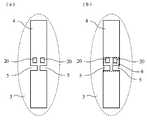
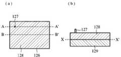
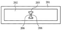
이하, 본 발명의 실시예1에 대해서 도1∼도6을 사용하여 설명한다. 도1은, 실시예1에 의한 RFID태그의 구성도, 도1(a)는, 유전체 기판의 표면도, 도1(b)는 유전체 기판의 선A-A’부분 단면도1, 도1(c)는, 유전체 기판의 선A-A’부분 단면도2, 도2는, RFID시스템의 기본구성도, 도2(a)는, RFID시스템도, 도2(b)는 RFID태그의 기능 블럭도, 도3은 RFID태그의 전계도, 도4는, 실시예1에 의한 RFID태그의 특성 임피던스도, 도5는, 실시예1에 의한 RFID태그의 전기 접속부 노출도, 도5(a)는, 2단자부 도면, 도5(b)는, 4단자부도, 도5(c)는 도5(a)(b)의 유전체 기판의 선A-A’부분 단면도, 도6은, 실시예1에 의한 RFID태그의 슬롯 확대도, 도6(a)는, IC칩 설치전, 도6(b)는, IC칩 설치후이며, 도1∼4에 있어서, 1은, 유전체 기판, 2는 유전체 기판(1)의 일주면(이면)에 형성된 접지 도체부, 3은, 유전체 기판(1) 다른 주면(표면)에 형성된 패치 도체부, 4는, 패치 도체부(3)의 일부에 형성된 길고 좁은형의 사각형의 슬롯, 5는 슬롯(4)의 대향부분으로부터 내부에 각각 연장되고, 패치 도체부(3)와 전기적으로 연속한 전기적으로 접속부, 6은, 슬롯(4)의 내부에 배치되고, 전기 접속부(5)에 접속된 IC칩, 7은, IC칩(6)에 형성된 전기 접속부(5)와의 접속 단자다. 이때, IC칩(6)의 특성 임피던스에 따라서는, 임피던스 정합을 취하기 때문에 필요한 슬롯(4)의 형상이 패치 도체부(3)의 치수보다도 길어질 경우가 있을 수 있으므로 슬롯(4)은 장세형으로 한정하는 것은 없다.EMBODIMENT OF THE INVENTION Hereinafter, Example 1 of this invention is described using FIGS. Fig. 1 is a configuration diagram of an RFID tag according to the first embodiment, Fig. 1 (a) is a surface view of a dielectric substrate, and Fig. 1 (b) is a cross-sectional view of part A1 'of the dielectric substrate, Fig. 1 (c). Is a cross-sectional view of part A-A 'of the dielectric substrate, FIG. 2 is a basic configuration diagram of the RFID system, FIG. 2A is an RFID system diagram, and FIG. 2B is a functional block diagram of an RFID tag. 3 is an electric field diagram of the RFID tag, FIG. 4 is a characteristic impedance diagram of the RFID tag according to the first embodiment, FIG. 5 is an exposure diagram of the electrical connection of the RFID tag according to the first embodiment, and FIG. Fig. 5 (b) is a four-terminal view, and Fig. 5 (c) is a cross-sectional view taken along the line A-A 'of the dielectric substrate of Fig. 5 (a) and (b). 6A is an enlarged view of the slot of the tag, before the IC chip is installed, and FIG. 6B is after the IC chip is installed. In FIGS. 1 to 4, 1 is a dielectric substrate and 2 is a
8은, RFID태그, 9는, RFID태그와 무선통신을 행하는 RFID리더 라이터, 10은, RFID 태그(8)에 설치된 안테나부, 11은, 안테나부(10)가 수신한 RFID리더 라이터(9)로부터의 송신파를 후단의 디지털 회로에 보내는 아날로그부, 12는, 송신파를 A/D변환하는 A/D변환부, 13은, 안테나부(10)가 수신한 송신파를 정류회로에서 평활화하고, 전력을 생성하는 RFID태그의 각 회로에 급전 및 전원제어를 행하는 전원제어부, 14는, RFID태그(8)에 탑재되고, 고체식별 정보 등의 태그 정보가 격납된 메모리부, 15는, 송신파를 복조하는 복조부, 16은, 복조부(15)에서 복조된 송신파에 의해 메모리부(14)를 포함한 IC칩(6)안의 회로를 제어하는 제어부, 17은, 제어부(16)에 의해 메모리부(14)로부터 인출된 정보를 변조하는 변조부, 18은, 복조부(15)·제어부(16)·변조부(17)에 의해 구성되는 디지털부, 19는, 변조부에서 온 신호를 D/A변환하고, 아날로그부(11)에 보내는 D/A변환부, 20은, 더미 패드부다. 이때, 패치 도체부(3)는, 사각형일 필요는 없고 원형이나 타원형이어도 좋다. 또한, RFID태그(8)에 있어서, 안테부(11)의 후단의 회로는 IC칩(6)안에 구축되어 있다. 도면 중, 동일한 부호는, 동일 또는 상당히 부분을 나타내 그것들에 관한 상세한 설명은 생략한다.8 is an RFID tag, 9 is an RFID reader / writer for wireless communication with the RFID tag, 10 is an antenna unit provided in the
우선, RFID시스템의 기본적인 동작에 대해서 도2를 사용하여 설명한다. RFID시스템을 이용하는 용도(생체·물품의 입퇴실관리나 물류관리)에 맞추고, 그것들의 태그 정보가 RFID태그(8)의 메모리부(14)에 격납되어 있고, RFID 리더 라이터(9)는, 자신의 송수신 에어리어내에 RFID태그(8)가 (입퇴실 관리나 물류관리의 대상인 생체·물품에 접착될 수 있고) 존재 또는 이동하고 있을 때에 태그 정보의 갱신·기록, 또는 판독을 행할 수 있다. RFID 리더 라이터(9)는, 갱신·기록, 또는 판독 등을 RFID 태그(8)에 명령하는 코맨드 신호를 송신파로서 RFID리더 라이터(9)의 안테나부로부터 RFID 태그(8)에 송신한다. RFID 태그(8)의 안테나부(10)가 송신파를 수신하고, 송신파는 전원제어회로(13)에 의해 검파·축전(평활화)되어, RFID 태그(8)의 동작 전원을 생성해, RFID 태그(8)의 각 회로에 동작 전원을 공급한다. 또한, 송신파는 복조부(15)에 의해 코맨드신호가 복조된다. 복조된 코맨드 신호의 명령 내용으로부터 제어부(16)가 데이터 처리하고, 메모리부(14)에 태그 정보의 갱신·기록과 판독 중 어느 한쪽, 또는 양쪽의 지시를 행하고, 이 제어부(16)의 지시에 의해 메모리부(14)가 출력한 판독 신호가 변조부(17)에 의해 변조된 회신파가 아날로그부(11)를 경유해서 안테나부(10)로부터 RFID 리더 라이터(9)의 안테나부에 송신되어, RFID 리더 라이터(9)가 판독 신호를 수신하고, 원하는 정보를 얻는다.First, the basic operation of the RFID system will be described with reference to FIG. According to the use of the RFID system (entry room management and logistics management), the tag information thereof is stored in the
다음에, 도1∼6을 사용해서 실시예1에 관련되는 RFID태그의 구조·제조 방법 및 동작을 설명한다. RFID 리더 라이터(9)와 무선통신하기 위한 RFID태그의 안테나부(10)를 형성하기 때문에, 유전체 기판(1)의 주면에 도체층을 형성한다(도체부 형성 공정). 일주면(이면)의 도체층은, RFID태그의 접지 도체부(2)로 하고, 다른 주면(표면)의 도체층은, 슬롯(4)을 갖는 패치 도체부(3)로 한다. 또한, 슬롯(4)에 의해, 패치 도체부(3)로부터 유전체 기판(1)이 노출해서 좋고, 유전체 기판(1)의 노출 부분은, 코팅 되어 있어도 된다. 슬롯(4)은, 패치 도체부의 3의 방사패턴이 양호해지도록 패치 도체부(3)의 중앙부에 형성되고(슬롯 형성 공정), 슬롯(4) 및 패치 도체부(3)의 촌법은, 패치 도체부(3)를 여진하기 때문에 RFID시스템의 사용 주파수와, 후술하는 IC칩(6)과의 임피던스 정합이 취해지게 조정되어 있다. 이때, 조 정에는 유전체 기판(1)의 두께나 비유전률도 크게 관계되므로, 이러한 조건도 맞춰서 조정해서 설계 함에 의해, 원하는 방사패턴이나 이득을 얻는다. 또한, 전기 접속부(5)는, 패치 도체부(3)의 일부에 형성되고, 슬롯(4)의 대향부분인 2변(도1에 도시되는 슬롯(4)의 긴변)으로부터 각각 패치 도체부(3)의 중앙을 향해서 연신하고, 패치 도체부(3)와 전기적으로 연속해서 형성되어 있고(전기 접속부 형성 공정), 슬롯의 형성과 동시에 형성해도 좋다. 도1(c)에 나타내는 IC칩(6)이 슬롯(4)내의 전기 접속부(5)끼리의 중앙에서, 기판의 두께 방향의 전계가 0의 위치에 배치되고, 접속 단자(7)에 의해 전기 접속부(5)에 전기적으로 접속되어 있다(접속 공정). 여기에서, 도체층(접지 도체부(2), 패치 도체부(3), 전기 접속부(5))은, 에칭·증착·밀링 등에 의한 형성이나 필름에 인쇄한 것을 유전체 기판(1)에 접착하는 등, 일반적인 프린트 기판의 가공 방법을 사용한다. 한편, IC 칩(6)은, 열압착 등의 수법을 사용해서 설치할 수 있으므로, 유전체 기판(1)의 주면(표면·이면)에 대한 가공만으로, 간편한 구조의 RFID태그를 제조할 수 있고, 수율의 저감·제조 코스트 다운이 가능하다. 또한, IC칩(6)의 접속 단자(7)와 전기 접속부(5)에의 설치시의 위치 결정은, 슬롯(4)의 중앙부근 근방에 미소 슬롯(도시되지 않음)을 설치하는 등 해서 행하면 좋고, 미소 슬롯은, RFID태그(8)의 전기 특성에 영향이 거의 없다.Next, the structure, manufacturing method, and operation of the RFID tag according to the first embodiment will be described with reference to Figs. Since the
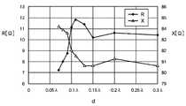
도3은, 접지 도체부(2)와 패치 도체부(3)와의 사이의 전계를 나타내고 있고, 이러한 전계가 도체 사이에서 형성되므로, 슬롯(4)의 대향부분의 사이에 전계가 달리고, 전위차가 생긴다. 따라서, 유전체 기판(1)의 두께 방향의 전계가 0의 위치를 IC칩의 급전점(전기 접속부(5))로 할 수 있고, 급전 손실을 대폭 저감할 수 있고, 패치 도체부(3)의 방사 패턴의 대칭성에 주는 악영향이 적고, 통신 가능거리가 향상한 RFID태그를 얻을 수 있다. 도4는, 접지 도체부(2)와 패치 도체부(3)와의 네 귀퉁이의 치수차이d의 변화에 의한 RFID 태그(8)의 특성 임피던스의 변화를 나타내고 있고, 가로축의 d는, 치수차이d를 RIFD태그의 사용 주파수의 파장비로 나타낸 것, 세로축의 R[Ω]과 Ⅹ[Ω]은, 각각 특성 임피던스의 실수부와 허수부를 가리키고 있다. 여기에서, 접지 도체부(2)와 패치 도체부(3)와의 치수차이는, 도1에 나타내는 패치 도체부(3)의 단부로부터 유전체 기판(1)(도4는, 유전체 기판(1)의 면적과 접지 도체부(2)는 면적이 마찬가지다)의 단부까지의 길이d를 가리키고 있다. 따라서, d가 0.1λ이상의 경우에, RFID태그(8)의 임피던스가 거의 일정해지는 것을 도4로부터 알 수 있으므로, d를 0.1 이상으로 함에 의해, RFID태그(8)의 설치 대상이 도체나 비도체에 관계되지 않고, 또한 공중에 띄웠을 경우이여도 성능이 열화하지 않고, RFID리더 라이터(9)와의 무선통신이 가능하게 된다.3 shows an electric field between the
여기에서, 실시예1에 관련되는 패치 도체부(3)에 여진되는 IC칩(6)을 갖는 RFID태그(8)를 전술의 RFID시스템의 기본적인 동작을 사용해서 설명하면 「RFID 리터 라이터(9)는, 갱신·기록, 또는 판독 등을 RFID태그(8)에 명령하는 코맨드 신호를 송신파로서 RFID리더 라이터(9)의 안테나부에서 RFID태그(8)에 송신한다. RFID태그(8)를 구성하는 유전체 기판(1)의 전파의 방사부인 패치 도체부(3)이 송신파를 수신하고, 슬롯(4)의 대향부분간에 전위차가 생기고, 송신파가 IC칩(6)에 공급된다. IC칩(6)에 공급된 송신파는, 전원제어회로(13)에 의해 검파·축전(평활화)되어, RFID 태그(8)의 동작 전원을 생성하고, RFID 태그(8)의 각 회로(IC칩(6))에 동 작 전원을 공급하고, 송신파로부터 코맨드 신호가 복조되어, 복조된 코맨드 신호의 명령 내용으로부터 메모리부(14)에 태그 정보의 갱신·기록과 판독 중 어느 한쪽, 또는 양쪽을 행하고, 메모리부(14)가 출력한 판독 신호가 회신파로서 IC칩(6)에 송신파가 공급된 경로와 같은 경로를 거슬러 오르고, 방사부인 패치 도체부(3)로부터 RFID 리더 라이터(9)에 회신파가 송신되고, RFID 리더 라이터(9)의 안테나부가 회신파를 수신하여, 원하는 정보를 얻는다」라고 하게 되어, RFID시스템의 기본적인 동작과 같은 동작이 문제없이 행해지는 것을 알 수 있다. 또한, RFID시스템이 행하는 무선통신의 데이터의 내용은, 종래부터의 내용이어도 좋고, 신규의 것이라도 좋고, 유전체 기판(1)의 이면에 접지 도체부(2)를 형성하고 있으므로, 유전체 기판(1)의 이면측을 설치 대상의 면을 향함으로써, 설치 대상이 도체나 비도체에 관계되지 않고 설치가 가능한 간이구조의 RFID태그를 저렴해서 제조할 수 있기 때문에, 대량의 RFID태그를 필요로 하는 물류관리, 창고관리, 기재관리, 자동차의 입퇴장 관리 등 폭넓은 분야에서 이용할 수 있고, 설치 대상이나 설치 대상의 면이 금속물체 등의 도체이여도 설치하는 것이 가능하다.Here, the
도5, 도6을 사용하여, 간이구조로 저렴한 제조가 가능한 RFID태그를 실현하기 위한 일요소인 IC칩(6)의 설치의 상세를 설명한다. 도5, 도6은, 도6(b)를 제외하고, 전기 접속부(5)에 IC칩(6)을 설치하기 전의 RFID태그(8)를 보이고 있다. 전기 접속부(5)는, 패치 도체부(3) 및 슬롯(4)을 형성할 때에 동시에 형성하면 효율적이지만, 그 형상과 치수는, 설치하는 IC칩(6)의 접속 단자(7)의 수와 특성 임피던스에 맞출 필요가 있다. 예를 들면, 임피던스 정합을 얻기 위해서, 슬롯(4)의 형 상의 미세 조정에 덧붙여, 접속 단자(7)의 발이 2개일 경우에는, 도5(a)에 나타나 있는 바와 같이, 슬롯(4)의 대향부분으로부터 각각 연신하고, 접속 단자의 임피던스 정합이 얻어지는 폭의 2개의 전기 접속부(5)를 형성하고, 접속 단자(7)의 발이 4개일 경우에는, 도5(b)에 나타나 있는 바와 같이, 슬롯(4)의 대향부분으로부터 각각 연신하고, 접속 단자의 임피던스 정합이 떨어지는 폭의 2개의 전기 접속부(5)를 형성하고, 접속 단자(7)의 발중 2개를 접속하고, 나머지의 2개의 발을 더미 패드부(20)에 접속한다. 더미 패드부(20)는, 도5(b), 도6(a)에 나타나 있는 바와 같이, 패치 도체부(3) 및 전기 접속부(5)와는 전기적으로 접속되지 않고 있다. 또한, 도6(b)는, IC칩(6)을 설치했을 경우의 IC칩(6)을 투시한 도면이고, 도6(b)로부터, 더미 패드부(20)는, 전기적으로뿐만 아니라 전파적으로도 독립적인 단순한 더미의 패드부에서, 접속 단자(7)의 나머지 2개의 발을 재치하기 위한 패드부인 것을 알 수 있다. 형성 방법은, 전기 접속부(5)를 형성할 때에 동시에 행하는 것이 효율적이고, 상기한 바와 같이, 일반적인 프린트 기판의 가공 방법을 사용할 수 있고, IC 칩(6)의 사양의 변경에 유연하게 대응할 수 있으므로, 간이구조의 RFID태그를 저렴하게 제조할 수 있다. 이때, 더미 패드부(20)의 수는, 2개로 한정된 것은 아니고, IC칩(6)의 접속 단자(7)의 수에 의해 설치하지 않은 경우도 있다.5 and 6, details of the installation of the
실시예2.Example 2.
본 발명의 실시예2에 대해서 도7∼도10을 사용하여 설명한다. 도7은, 실시예2에 의한 RFID태그의 구성도, 도8은, 실시예2에 의한 RFID태그의 구성도, 도9는 실 시예2에 의한 RFID태그의 슬롯 확대도, 도9(a)는, IC칩 설치전, 도9(b)는, IC칩 설치 후, 도10은, 실시예2에 의한 RFID태그의 구성도이며, 도7∼도10에 있어서, 21은, 패치 도체부(3)의 단부에 홈 모양으로 설치된 전기장 조정부, 22는, IC칩(6)이 배치된 위치부터 상반 방향으로 폭이 넓어지도록 형성한 테이퍼 형의 슬롯, 23은, 패치 도체부(3)의 변에 대하여 각도를 갖게 형성되고, 패치 도체부(3)에 축퇴분리 방식을 사용해서 원편파를 방사시키는 슬롯이다. 도면 중, 동일한 부호는, 동일 또는 상당부분을 나타내고 그것들에 관한 상세한 설명은 생략한다.
도7∼도10을 사용해서 실시예2에 관련되는 RFID태그의 구조 및 동작을 설명한다. 이때, 실시예2에서는, RFID태그의 전기장 조정 방법·광대역화·축퇴분리에 따른 원편파 송수신에 관한 것으로서, 기본적인 구성이나 발명의 효과는, 실시예1과 마찬가지이다. 도7은, RFID태그의 전기장 조정 방법에 관한 것으로서, 도1의 RFID태그와의 큰 차이는, 도면에 나타나 있는 바와 같이, 패치 도체부(3)의 측부에 절결과 같은 형상의 전기장 조정부(21)가 형성된 패치 도체부(3)이다. 전기장 조정부(21)는, 슬롯(4)과는 수직이 되는 위치에 설치되어 있기 때문에, 패치 도체부(3)의 실효적인 전기장이 명백한 길이보다도 길어져, RFID 시스템의 사용 주파수가 고정이어도, 패치 도체부(3)의 크기를 작게 할 수 있으므로, RFID태그(8) 전체의 치수를 작게 할 수 있다. 패치 도체부(3)의 길이미만이면, 전기장 조정부(21)의 길이는 변경할 수 있으므로, 길이나 절입의 정도를 조정해서 설계 함에 의해, RFID태그(8) 전체의 치수를 명함대로 하는 것이나 설치 대상에 맞춘 치수로 하는 것도, 어느 정도의 범위내에서는 가능하다. 이때, 전기장 조정부(21)의 조정이외에도, 실 시예1과 마찬가지로, 유전체 기판(1)의 두께나 비유전율, 패치 도체부(3), 슬롯(4)의 치수 등이 크게 관계되므로, 이러한 조건도 맞춰서 조정해서 설계 함에 의해, RFID태그(8)의 치수 및 원하는 방사패턴이나 이득을 얻을 수 있다. 또한, 패치 도체부(3)의 한쪽에만 설치해도 된다.7 to 10, the structure and operation of the RFID tag according to the second embodiment will be described. At this time, the second embodiment relates to circular polarization transmission and reception according to the electric field adjustment method, wideband and degenerate separation of RFID tags, and the basic configuration and effects of the invention are the same as those of the first embodiment. FIG. 7 relates to a method for adjusting an electric field of an RFID tag, and a large difference from the RFID tag of FIG. 1 is that, as shown in the drawing, an electric
도8, 도9는, RFID태그의 광대역화에 관한 것으로, 슬롯(22)은 IC칩(6)이 배치된 위치부터 상반 방향으로 폭이 넓어져 가는 테이퍼 모양으로 되어 있다. 도1의 슬롯(4)과 비교하면, 슬롯(4)의 대향부분이 전기접속부(5)를 제외하고, 상반 방향과 함께 일정한 폭이 형성되어 있다. 이렇게 슬롯(22)이 테이퍼 형을 이루고 있는 것에 의해, RFID태그의 사용 주파수의 광대역화가 실현되고, 대역은 테이퍼의 넓어지는 치수를 조정하는 것에 의해 선택이 가능하다. 따라서, RFID시스템의 통신 가능대역을 광대역화할 수 있기 때문에, 임피던스 정합이 용이하고 제조 오차에 의한 수율의 악화를 저감할 수 있을 뿐만 아니라, RFID태그(8)가 설치한 주위의 환경에 의해 물방울이나 오물이 부착되어서 임피던스 변화에 강한 내환경성을 가진 RFID태그를 얻을 수 있다. 또한, 도9(a)(b)에 도시한 바와 같이, IC칩의 설치는, 실시예1의 도6(a)(b)의 설명과 같으므로, 설명은 생략한다. 더미 패드부(20)는, IC칩(6)에 설치된 접속 단자(7)의 발의 수에 의하여, 필요가 없는 경우도 있다.8 and 9 are related to the widening of the RFID tag, and the
도10은, RFID태그의 축퇴분리에 의한 원편파 송수신에 관한 것으로서, 도1의 RFID태그와의 큰 차이는, 도10에 나타나 있는 바와 같이, 슬롯(23)의 위치가 패치 도체부(3)에 대하여, 경사지게 설치된다. 도1의 슬롯(4)과 비교하면, 슬롯(23)은, IC칩(6)을 중심으로 해서 약 45도 경사지게 형성된다(경사시키는 방향은, 송수신 하는 전파가, 우선성인가 좌선성인가에 의해 결정한다). 이러한 위치에 설치되어 있기 때문에, 슬롯(23)은 패치 도체부(3)의 축퇴분리 소자(섭동소자)로서 동작한다. 즉, 근사적으로, 도1의 RFID태그의 방사패턴에 같은 방사패턴의 위상을 π/2 비켜 놓아서 포갠 방사패턴에 가까운 방사패턴을 갖는 원편파가 송수신 가능한 RFID태그가 얻어지므로, RFID시스템의 무선통신에 원편파의 전파가 사용되어도 대응이 가능해진다. 이때, 일반적으로, 축퇴분리 소자는 패치 도체부(3)에 대하여, 약 45도 정도 경사해서 형성시키지만, 급전점의 영향으로 양호한 방사패턴을 얻기 위해서는, 경사각도를 약 45도가 아니고, 미세 조정을 행할 필요가 있다. 그러나, 본 발명은, 급전점(IC칩(6))을 전계가 0이 되는 위치에 설치하고 있으므로, 비교적, 미세 조정의 폭이 좁아져, 조정이 용이해진다. 한층 더, 실시예2에 있어서의 RFID태그의 전기장 조정방법·광대역화·축퇴분리에 의한 원편파 송수신은, 각각을 조합해서 실시하는 것이 가능하다.FIG. 10 relates to circular polarization transmission and reception by degenerate separation of an RFID tag. As shown in FIG. 10, a large difference from the RFID tag of FIG. It is installed inclined with respect to. Compared with the
실시예3.Example 3.
본 발명의 실시예3에 대해서 도11, 도12를 사용하여 설명한다. 도11은, 실시예3에 의한 RFID태그의 구성도, 도11(a)는, RFID태그의 패치 도체면, 도11(b)는, RFID태그의 접지 도체면(접착층 없음), 도11(c)는, RFID태그의 접지 도체면(접착층 있음), 도12는, 실시예3에 의한 RFID시스템의 구성도이며, 도11, 도12에 있어서, 24는, 접착층, 25는, 설치면이다. 도면 중, 동일한 부호는, 동일 또는 상당부분을 나타내고 그것들에 관한 상세한 설명은 생략한다. 도11의 RFID태그(8)는, 접지 도 체부(2)의 표면에 접착층(24)을 설치한 것으로, 접착층(24)은, 접착제, 양면 테이프 등을 사용하면 좋고, 접착이 가능하면 도포의 방법은 자유스럽다. 도12에 나타내는 설치면(25)은, 금속이나 비금속에 관계되지 않고 물류관리, 창고관리, 기재관리, 자동차의 입퇴장 관리 등의 용도에 따른 물품 등의 표면이다. 설치면(25)에 접착층(24)을 접착된 RFID태그(8)는, RFID리더 라이터(9)와 무선통신을 행하는 것이 가능한 것은, 패치 도체부(3)가, 유전체 기판(1)보다도 면적이 작으므로, 접지 도체나 RFID태그(8)의 설치 위치가 도체상이었을 경우의 영향에 의한 RFID태그(8)의 특성 임피던스의 변화가, 상기한 바와 같은 RFID태그(8)의 구조를 얻으므로 적기 때문이다. 따라서, 설치면(25)이 금속이나 비금속으로 설치가능한 RFID태그의 설치 방법을 얻을 수 있다. 이때, 통신 거리는, RFID태그(8)의 치수 등에 의해 변화한다.A third embodiment of the present invention will be described with reference to Figs. 11 and 12. Fig. 11 is a configuration diagram of the RFID tag according to the third embodiment, Fig. 11 (a) is a patch conductor surface of the RFID tag, and Fig. 11 (b) is a ground conductor surface (no adhesive layer) of the RFID tag, c) is a ground conductor surface (with adhesive layer) of an RFID tag, FIG. 12 is a configuration diagram of the RFID system according to the third embodiment, and in FIGS. 11 and 12, 24 is an adhesive layer and 25 is an installation surface. . In the drawings, the same reference numerals denote the same or equivalent parts and detailed description thereof will be omitted. The
실시예4.Example 4.
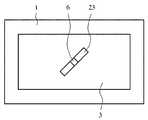
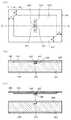
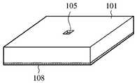
본 발명의 실시예4에 대해서, 이하에 설명한다. 도13은, 이 실시예4에 관련되는 RFID태그의 구성도다. 도13(a)는, RFID태그의 평면도, 도13(b)는, 도13(a)에서 A-A’선에 의해 절단했을 때의 단면도, 도13(c)는, 도13(b)의 분해 단면도다. 이것들의 도13에 있어서, 101은, 예를 들면 올레핀계 열가소성 엘라스토머에 의하여 구성하고 있는 유전체 기판이다. 102는, 유전체 기판(101)의 일주면(표면)상에 설치되는 필름 기본재료다. 이 필름 기본재료(102)는, 필름 폴리에틸렌테레프탈레이트, 폴리이미드, 폴리에틸렌나프타레이트, 폴리염화비닐 등을 사용할 수 있다. 또한, 필름 기본재료(102)는, 그 밖의 유연성이 있는 것이어도, 그렇지 않은 기판이라고 할 수 있는 것이어도 좋고, 또한 투명이라도 유색 반투명성의 것이라도 좋다. 또한, 도13(a)에서는, 필름 기본재료(102)가 투명성일 경우에, 필름 기본재료(102)를 통과시켜서 보이는 상태를 도시하고 있다. 여기에서는, 필름 기본재료(102)와 유전체 기판(101)과는 평면에 있어서 동일치수로 하고 있다. 103은, 필름 기본재료(102) 위에 설치된 도체 패턴이다. 도체 패턴(103)은, 도13(a)에 나타나 있는 바와 같이 필름 기본재료(102)의 세로 및 가로의 단부로부터 거리d만큼 사이를 떼서 그 내측에 형성하고 있다. 이 경우, 도체 패턴(103)은, 유전체 기판(101)의 세로 및 가로의 단부로부터 거리d만큼 사이를 떼서 형성하고 있다고도 할 수 있다. 한편, 필름 기본재료(102)를 유전체 기판(101)의 세로 및 가로의 단부로부터 거리d만큼 사이를 떼서, 유전체 기판의 일주면 위에 배치할 수도 있다. 이 경우, 도체 패턴(103)은, 필름 기본재료(102)상의 전체면에 설치할 수도 있다. 도체 패턴(103)의 중앙부에는, 도13(a)에 나타나 있는 바와 같이, 가늘고 긴 형상의 슬롯(104)을 형성하고 있다. 이 슬롯(104)은, 도체 패턴(103)을 에칭 처리에 의해 형성할 수 있다. 그리고, 이 슬롯(104)의 길이 및 폭은 사용 주파수에 의해 결정할 수 있다. 105는, 유전체 기판(101)의 일주면에 형성한 구멍부다. 106은, IC칩에서, 후술하는 것 같은 메모리 등으로 구성하고 있다. 이 IC칩(106)은, 슬롯(104)을 거쳐서 도체 패턴(103)에 전기적으로 접속하고 있다.
여기에서, IC칩(106)과 도체 패턴(103)과의 접속 구성에 관하여 설명한다. 107은, 도13(a) 및 (b)에 나타나 있는 바와 같이, 슬롯(104)의 양측에 있어서의 도 체 패턴(103)으로부터 슬롯(104)의 내부에 연장되는 돌기형의 전기 접속부에서, 각각 슬롯(104)의 양측에 있어서의 도체 패턴(103)에 연속적으로 연결되어서 전기적으로 접속하고 있다. 이것들의 전기 접속부(107)은, 에칭에 의해 도체 패턴(103)의 형성과 동시에 형성하면 좋다. IC 칩(106)의 단자(도시 생략)는, 그것들의 전기 접속부(107)에 접속하게 된다. IC 칩(106)의 사이즈가 슬롯(104)의 폭과 같은 정도 또는 이것보다 작을 경우에는, 슬롯(104)의 폭내에 들어가게 되지만, 이 때에, IC칩(106)의 단자(도시 생략)는 전기 접속부(107)와 접속한다. 그런데, IC칩(106)의 사이즈가 슬롯(104)의 폭보다도 클 경우에는, IC칩의 단자(도시 생략)는 슬롯을 통하는 도체 패턴(103)의 슬롯(104)에 가까운 부분에 전기적으로 접속하면 좋다. 따라서, 이 경우에는, 상기한 바와 같은 전기 접속부(107)를 설치할 필요는 없게 된다.Here, the connection structure of the
또한, 도13(a)에 있어서는, IC칩(106)은, 슬롯(104)의 길이방향에 있어서 중앙부에 배치하고 있지만, 그 중앙부가 아니고 슬롯(104)의 길이방향의 단부에 배치해도 좋다. 상기 유전체 기판(101)의 구멍부(105)는, IC칩(106)을 삽입하기 위해서 형성했으므로, 그 깊이나 그 폭은 IC칩의 크기에 대응한 것이 된다. 그리고, 그 구멍부(105)를 형성하는 위치에 대해서는, 슬롯(104)의 어느 위치에 IC칩(106)을 배치하는가에 따라 결정되는 것은 당연하다. 어떻든간에, 슬롯(104)의 형상과 치수는, 설치하는 IC칩(106)의 전기 접속부(107)의 수와 특성 임피던스에 맞출 필요가 있다. 예를 들면, 임피던스 정합을 얻기 위해서, 슬롯(104)의 형상의 미세 조정에 더해서, IC칩(106)의 접속 단자의 발이 2개의 경우에는, 임피던스 정합이 얻어지는 폭의 2개의 전기 접속부(107)를 형성하면 좋다. 다음에, 108은, 유전체 기판(101)의 타주면(이면)에 설치한 접지 도체 패턴이다. 109는, 유전체 기판(101)과 필름 기본재료(102)를 접착하는 접착 시트(sheet)이다. 접착 시트(109)는, 도13(c)에 나타낸 것처럼, 유전체 기판(101) 위이며, 구멍부(105)이외의 부분에 대응하는 부분에 설치하고, 유전체 기판(101)과 필름 기본재료(102)를 접착, 고정 할 수 있다. 또한, 유전체 기판(101)과 필름 기본재료(102)를 고정하기 위해서는, 접착 시트(109)가 아니어도, 접착제를 사용할 수도 있다.In Fig. 13A, the
도14(a)는, RFID태그와 RFID리더 라이터와의 사이에서 송수신을 행하는 모양을 모식적으로 나타낸 개념도다. 도14(b)는, RFID태그의 구성도이며, 특히, IC칩(106)의 내부 구성을 기능적으로 나타낸 블록 구성도다. 도14(a)(b)에 있어서, 110은, 도13에 나타낸 구성의 RFID태그다. 111은, RFID태그(110)에 설치된 안테나부에서, 도13에 있어서 슬롯(104)을 형성한 도체 패턴(103)에 해당하는 것이다. RFID 태그(110)의 안테나부(111)는, 전술한 도13(a) 및 (b)에 나타나 있는 바와 같이, 유전체 기판(101)의 일주면(표면)에 슬롯(104)을 갖는 도체 패턴(103)을 설치하고, 유전체 기판(101)의 타주면(이면)에 접지 도체 패턴(108)을 설치하고 있으므로, RFID태그(110)는 패치 안테나로서 기능하는 것이다. 즉, 슬롯(104)을 갖는 도체 패턴(103)이 안테나 패턴(방사부)로서 기능한다. 그리고, 도체 패턴(103)과 슬롯(104)은, 여진하도록 RFID시스템의 사용 주파수와 IC칩(106)과의 임피던스 정합을 얻도록 조정하고 있다. 이 조정은, 유전체 기판(101)의 두께나 비유전률에도 크게 관계되므로, 이러한 조건도 맞춰서 조정, 설계하는 것에 의하여, 원하는 방사패 턴이나 이득을 얻을 수 있다. 또한, 슬롯(104)은, 도체 패턴(103)의 방사패턴이 양호해지도록 도체 패턴(103)의 중앙부에 형성하고 있는 것은 상술한 대로이다. 이러한 조건을 맞추어서 조정해서 설계 함으로써, RFID태그(110)에 있어서의 원하는 방사패턴이나 이득을 얻을 수 있고, RFID 태그(110), 즉, 유전체 기판(101)을 대형화하지 않고, 예를 들면, 1∼8m정도의 통신 거리를 얻는 것이 가능해진다.Fig. 14A is a conceptual diagram schematically showing how transmission and reception are performed between an RFID tag and an RFID reader / writer. Fig. 14B is a block diagram of the RFID tag, and in particular, a block diagram functionally showing the internal structure of the
또한, 112는, RFID리더 라이터, 113은, RFID리더 라이터(112)에 설치된 안테나부에서, RFID태그(110)의 안테나부(111)와 무선통신을 행하는 것이다. 106은, 도13에서 설명한 IC칩이며, 그 구체적 구성에 대해서는, 도14(b)에 도시한 구성으로 하고 있다. 114는, RFID리더 라이터(112)로부터의 송신파를 RFID태그(110)의 안테나부(111)에 의해 수신하고, 후단의 디지털 회로(121)에 출력하는 아날로그부이다. 115는, 송신파를 A/D변환하는 A/D변환부, 116은, 안테나부(111)가 수신한 송신파를 정류회로에서 평활화해서 전력을 생성하고, RFID 태그(110)의 각 회로에 급전 및 전원제어를 행하는 전원제어부다. 117은, RFID태그(110)에 탑재되어, 고체식별 정보등의 태그 정보가 격납된 메모리부다. 118은, 송신파를 복조하는 복조부, 119는, 복조부(118)에서 복조된 송신파에 의해 메모리부(117)를 포함한 IC칩(106) 안의 회로를 제어하는 제어부다. 120은, 제어부(119)에 의해 메모리부(117)로부터 인출된 정보를 변조하는 변조부다. 121은, 복조부(115), 제어부(116) 및 변조부(117)로 구성되는 디지털부, 122는, 변조부(120)로부터 송신되어 온 신호를 D/A변환하고, 아날로그부(114)에 출력하는 D/A변환부다.In addition, 112 is an RFID reader / writer, 113 is an antenna part provided in the RFID reader /
여기에서, 이러한 RFID시스템에 대해서, 그 기본적인 동작에 관하여 설명한 다. 이러한 RFID시스템을 이용하는 용도(생체·물품의 입퇴실 관리나 물류관리)에 맞추어서, 그것들의 태그 정보가 RFID태그(110)의 메모리부(117)에 격납되고, RFID 리더 라이터(112)는, 자신의 송수신 에어리어내에 RFID태그(110)가 (입퇴실관리나 물류관리의 대상인 생체·물품에 접착되어) 존재 또는 이동하고 있을 때에 태그 정보의 갱신·기록, 또는 판독을 행할 수 있다. RFID 리더 라이터(112)는, 갱신·기록, 또는 판독 등을 RFID태그(110)에 명령하는 코맨드 신호를 송신파로서 RFID리더 라이터(112)의 안테나부(113)로부터 RFID태그(110)의 안테나부(111)에 송신한다. RFID 태그(110)의 안테나부(111)가 송신파를 수신하고, 송신파는 전원제어부(116)에 의해 검파·축전(평활화)되어, RFID 태그(110)의 동작 전원을 생성하고, RFID태그(110)의 각 회로에 동작 전원을 공급한다. 또한, 송신파는 복조부(118)에 의해 코맨드 신호가 복조된다. 복조된 코맨드 신호의 명령 내용으로부터 제어부(119)가 데이터 처리하고, 메모리부(117)에 태그 정보의 갱신·기록과 판독 중 어느 한쪽, 또는 양쪽의 지시를 행하고, 이 제어부(119)의 지시에 의해 메모리부(117)가 출력한 판독신호가 변조부(120)에 의해 변조된 회신파가 아날로그부(114)를 경유해서 안테나부(111)로부터 RFID리더 라이터(112)의 안테나부(113)에 송신되어, RFID 리더 라이터(112)가 판독신호를 수신하고, 원하는 정보를 얻는다.Here, the basic operation of such an RFID system will be described. According to the purpose of using such an RFID system (entry room management and logistics management), the tag information is stored in the
한층 더, 실시예4에 관련되는 RFID태그를 사용한 RFID시스템의 동작에 대해서, 상세하게 설명하면, RFID리더 라이터(112)는, 갱신·기록, 또는 판독 등을 RFID 태그(110)에 명령하는 코맨드 신호를 송신파로서 RFID리더 라이터(112)의 안테나부(113)로부터 RFID태그(110)의 안테나부(111)에 송신한다. RFID 태그(110)를 구성하는 유전체 기판(101)의 전파의 방사부인 도체 패턴(103)이 송신파를 수신하고, 슬롯(104)의 대향부분간에 전위차가 생기고, 송신파가 IC칩(106)에 공급되어, 상기와 같이, IC칩(106)에 공급된 송신파는, 전원제어부(116)에 의해 검파·축전(평활화)되어, RFID태그(110)의 동작 전원을 생성하고, RFID 태그(110)의 각 회로(IC칩(106))에 동작 전원을 공급하고, 송신파로부터 코맨드 신호가 복조되고, 복조된 코맨드 신호의 명령 내용으로부터 메모리부(117)에 태그 정보의 갱신·기록과 판독 중 어느 한쪽, 또는 양쪽을 행하고, 메모리부(117)가 출력한 판독 신호가 회신파로 해서, IC 칩(106)에 송신파가 공급된 경로와 같은 경로를 거슬러 오르고, 방사부인 도체 패턴(103)으로부터 RFID리더 라이터(112)에 회신파가 송신되고, RFID 리더 라이터(112)의 안테나부(113)가 회신파를 수신하여, 원하는 정보를 얻게 된다. 이때, RFID 시스템이 행하는 무선통신의 데이터의 내용은, 종래로부터 것이어도 좋고, 신규의 것이어도 좋고, 유전체 기판(101)의 이면에 접지 도체 패턴(108)을 형성하고 있으므로, 유전체 기판(101)의 이면측을 설치 대상의 면을 향함으로써, 설치 대상이 도체나 비도체에 관계되지 않고 설치가 가능한 간이구조의 RFID태그를 저렴하게 제조할 수 있기 때문에, 대량의 RFID태그를 필요로 하는 물류관리, 창고관리, 기재관리, 자동차의 입퇴장 관리 등 폭넓은 분야에서 이용할 수 있고, 설치 대상이나 설치 대상의 면이 도전성 물체 등의 도체이어도 설치하는 것이 가능하다.Further, the operation of the RFID system using the RFID tag according to the fourth embodiment will be described in detail. The RFID reader /
다음에, 도15(a)∼(e)에서, 실시예4에 관련되는 RFID태그의 제조 방법에 대해서, 그 단면도를 바탕으로 각 제조 공정을 설명한다. 도15(a)에 있어서는, 필름 기본재료(102) 위(필름 기본재료(102)의 이면측)에 도체층(123)을 형성하는 도체층 형성 공정을 나타낸 것이다. 그리고, 도15(b)에 나타나 있는 바와 같이, 도체 패턴(103)을 형성해야 할 영역 및 슬롯(104)의 내측에 전기 접속부(107)를 형성해야 할 영역을 마스크 하고, 에칭 등에 의해 도체 패턴(103) 및 전기 접속부(107)를 동시에 형성하는 도체 패턴형성공정을 나타낸 것이다. 이때, 필름 기본재료(102)에 도체층 형성 공정을 행하지 않고, 도체 패턴을 필름 기본재료(102)에 인쇄해도 좋다. 다음에, 도15(c)(d)에 나타나 있는 바와 같이, IC칩 접속 공정에서는, IC칩(106)의 접속 단자(124)를 전기 접속부(107)에 납땜에 의해 전기적으로 접속한다. 이 전기적인 접속 방법으로서는, 리플로우에 의한 열압착이 일반적이지만, 그 밖의 방법에 의해 접속해도 좋다. 한편, 유전체 기판(101)의 타주면(이면측)에는, 도15(e)에 나타나 있는 바와 같이, 접지 도체 패턴(108)을 형성하는 동시에, 일주면(표면측)에는, IC칩을 삽입하는 구멍부(105)를 형성한다. 이 구멍부(105)의 형성은, 예를 들면 사출 성형법에 의해 형성한다. 그 후에, 도15(e)에 나타나 있는 바와 같이, 필름 지지 공정(고착공정)에서는, 유전체 기판(101)의 일주면측에 있어서, 구멍부(105)를 제외한 접착 시트(109)를 접착한다. 이렇게, 접착 시트(109)를 접착한 유전체 기판(101)에 대하여, 필름 기본재료(102)에 도체 패턴(103) 및 IC칩(106)을 부착한 것을, 구멍부(105)에 IC칩(106)을 삽입하도록 포개고, 접착 시트(109)에 의해 유전체 기판(101)에 대하여 필름 기본재료(102)를 지지한다. 이렇게 해서, RFID태그(110)를 구성한다.Next, in Figs. 15A to 15E, the manufacturing process of the RFID tag according to the fourth embodiment will be described based on the cross sectional view. In Fig. 15A, the conductor layer forming step of forming the
또한, 도16∼도19에서, 실시예4에 관련되는 RFID태그의 제조 방법에 대해서, 그 평면도를 바탕으로 각 제조 공정을 설명한다. 도16은, 필름 기본재료의 전체면에 도체층을 형성한 평면도다. 도17(a)는, 도체 패턴(103) 및 슬롯(104)을 형성한 후의 필름 기본재료(102)의 이면도다. 도16에 나타나 있는 바와 같이, 필름 기본재료(102)의 이면측에 전면적으로 도체층(123)을 형성한 것에 있어서, 필름 기본재료(102)의 단부로부터 소정 거리d만큼 사이를 뗀 주위부분과 전기 접속부(107)를 제외한 슬롯(104) 부분의 도체층을, 예를 들면 에칭 처리 등에 의해 제거한 도체 패턴(103)의 구성을 도시하고 있다. 이때의 필름 기본재료(102)의 표면에서 보았을 때의 필름 기본재료(102)의 구성을 도17(b)에 보이고 있다. 필름 기본재료(102)가 투명 또는 반투명인 경우다. 또한, 도18(a)는, 필름 기본재료(102)상의 슬롯(104)의 내측에 IC칩(106)을 부착한 상태의 이면도다. 도18(b)는, IC칩을 필름 기본재료(102)에 부착한 상태를 필름 기본재료(102)의 표측으로부터 보았을 때의 상태도이며, 전기 접속부(107)와 IC칩(106)이 투명 또는 반투명의 필름 기본재료(102)를 통과시켜서 보이고 있다. 도19는, 유전체 기판(101)의 일주면에 IC칩(106)을 삽입하기 위한 구멍부(105)를 형성한 유전체 기판(101)의 평면도이다. 이때, 이 구멍부(105)는, 상기의 사출 성형법 이외에, 에칭이나 밀링 등에 의해 형성해도 좋다. 그리고, 상기한 바와 같이, 그 후에, 필름 기본재료(102)에 부착한 IC칩(106)을 유전체 기판(101)의 구멍부(105)에 삽입하도록 해서 필름 기본재료를 유전체 기판(101)에 지지 함에 의해, RFID태그를 완성시킨다.16 to 19, the manufacturing process of the RFID tag according to the fourth embodiment will be described based on the plan view. Fig. 16 is a plan view of a conductor layer formed on the entire surface of the film base material. Fig. 17A is a rear view of the
이상과 같이, 실시예4에 관련되는 RFID태그는, IC칩(106)이 유전체 기판(101)의 일주면에 형성한 구멍부(105)에 삽입하도록 구성했으므로, 필름 기본재 료(102)의 휨이나 팽창이 생기기 어려워져, 그 때문에 RFID태그에 충격 등이 가해진 경우에도, IC 칩(106)의 파손이나 IC칩(106)과 전기 접속부(107)와의 전기적인 접촉 불량이나 접속의 파단 등의 발생율을 대폭 저감시킬 수 있다. 또한, 유전체 기판(101)의 구멍부의 치수를 어떻게 할지는, IC칩(106)의 용적에 대하여 IC칩(106)을 구멍부(105)에 삽입할 때의 수율을 고려해서 설치하면 좋다. 이때, 사출성형법을 사용하고 있지 않은 유전체 기판(101)에 구멍부(105)를 형성할 때는, 유전체 기판(101)의 일주면을 절삭하는 방법에 의해 형성하면 좋다.As described above, the RFID tag according to the fourth embodiment is configured such that the
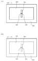
도20은, 실시예4에 관련되는 RFID태그의 전계(화살표로 기입)를 나타낸 전계도이다. 도20에는, IC칩(106) 주변의 부분 확대도도 병행하여 나타냄과 동시에, 그 부분 확대도에 있어서 화살표로 전계의 모양을 보이고 있다. 도20에 나타낸 화살표는, 접지 도체 패턴(108)과 도체 패턴(103)과의 사이의 전계를 나타내고 있고, 이러한 전계가 도체간에 형성되기 때문에, 슬롯(104)의 대향부분의 사이에 전계가 달리고, 전위차가 생긴다. 유전체 기판(101)의 두께 방향에 있어서의 전계의 강도가 0의 위치를 IC칩의 급전점으로 하고 있다. 도20에 나타나 있는 바와 같이, 유전체 기판(101)의 내부에 있어서, 좌우의 전계가 상호 상쇄하기 때문에, 슬롯(104)의 종축방향(도20에서는, 깊이 방향)의 축에 따른 위치에서는, 전계의 강도는 0이 된다. 따라서, 이 위치에 IC칩(106)의 전기 접속부(107)를 배치하면, 급전 손실을 대폭 저감할 수 있다. 따라서, 이렇게 구성하면, 도체 패턴(103)의 방사패턴의 대칭성에 악영향을 주는 것도 적고, 통신가능한 거리도 크게 연장시킬 수도 있고, 또한 구성이 간단하여도, 성능이 대폭 향상한 RFID태그를 얻을 수 있다고 하는 효과를 나타 낸다.Fig. 20 is an electric field diagram showing the electric field (written in arrows) of the RFID tag according to the fourth embodiment. In Fig. 20, a partial enlarged view of the periphery of the
도21은, 실시예4에 관련되는 RFID태그(110)에 있어서의 특성 임피던스의 변화의 모양을 나타낸 특성도다. 전기한 바에서는, 필름 기본재료(102)의 단부로부터 소정 거리d만큼 사이를 떼서 도체 패턴(103)을 형성하는 취지를 기재했지만, 이것은, 유전체 기판(101)의 타주면의 전체면에 접지 도체 패턴(108)을 형성하고 있기 때문에, 소정거리d는, 도20에 나타나 있는 바와 같이, 도체 패턴(103)과 접지 도체 패턴(108)과의 네 귀퉁이에 있어서의 치수차이라고 하는 것이 생긴다. 이렇게 하면, 소정거리d는, 접지 도체 패턴(108)이 유전체 기판(101)의 타주면의 전체면에 형성하지 않고 있는 경우이여도, 동일하게 도체 패턴(103)과 접지 도체 패턴(108)과의 네 귀퉁이에 있어서의 치수차이로서 생각할 수 있다. 그래서, 도21에 있어서, 가로축은 소정거리 또는 상기 한 치수차이d를 RIFD태그의 사용 주파수의 파장비를 의미한 것이고, 세로축 R[Ω] 및 Ⅹ[Ω]은 각각 특성 임피던스의 실수부 및 허수부를 나타낸 것이다. 다만, 가로축의 λ는 사용 주파수의 파장이다. 도21의 특성도에 따르면, 소정거리d가 0.13λ이상일 경우에는, RFID태그(110)의 특성 임피던스가 거의 일정해지고 있다. 따라서, 소정거리d를 0.13λ이상으로 함으로써, RFID태그의 설치 대상이 도체 또는 비도체의 물체에 상관없고, 또한 공중에 띄운 것 같은 상태이여도, RFID태그의 특성 임피던스가 거의 일정하기 때문에, RFID의 성능이 열화할 일이 없고, RFID 리더 라이터(112)와의 무선통신을 가능하게 할 수 있다. 또한, 유전체 기판(101)의 구멍부(105)의 위치에 있어서의 전계의 강도가 0의 위치이기 때문에, 구멍부(105)가 없는 경우에 있어서의 RFID태그의 특성 임피던스 변화와 거의 마찬가지라고 할 수 있다.Fig. 21 is a characteristic diagram showing a change of characteristic impedance in the
실시예5.Example 5.
다음에, 본 발명의 실시예5에 대해서, 도22, 도23을 사용하여 설명한다. 도22는, 실시예5에 관련되는 RFID태그의 구성을 나타낸 평면도이며, 도23은, 도22에 나타낸 슬롯 부근을 확대한 평면도다. 도23(a)는 IC칩이 미설치일 경우의 평면도이고, 또한, 도23(b)는 IC칩이 설치된 경우의 평면도다. 여기에서는, 실시예4의 경우에는, 접속 단자(124)가 2개, 즉, 발이 2개의 IC칩을 사용했을 경우에 관해서 설명했지만, 접속 단자(124)가 4개의 IC칩을 설치할 경우에는, 실시예4에서 설명한 2개의 전기 접속부(107)의 이외에, 2개의 더미 패드(125)를 슬롯(104)에 내측에 있어서, 접속 단자의 근방에 설치하고 있다. 이것들의 더미 패드(125)의 형성 방법은, 전기 접속부(107)를 형성함과 동시에, 형성한다. 또한, 도22, 도23으로부터 필름 기본재료(102)를 통과시켜서 보이는 더미 패드(125)는, 도체 패턴(103) 및 전기 접속부(107)와는 전기적으로 접속되지 않고 있는 단순한 더미로서의 패드다. 이와 같이, RFID에 설치하는 IC칩(106)의 사양의 변경에 유연하게 대응할 수 있으므로, 간이구조의 RFID태그를 저렴하게 제조할 수 있다. 또한, 더미 패드(125)의 수는, 2개에 한정된 것이 아니다.Next, Example 5 of this invention is demonstrated using FIG. 22, FIG. FIG. 22 is a plan view showing the configuration of the RFID tag according to the fifth embodiment, and FIG. 23 is an enlarged plan view of the vicinity of the slot shown in FIG. FIG. 23A is a plan view when the IC chip is not installed, and FIG. 23B is a plan view when the IC chip is installed. Here, in the case of the fourth embodiment, the case where two
실시예6.Example 6.
본 발명의 실시예6에 대해서, 도24∼도31을 사용해서 사출 성형에 의한 접지 도체 패턴(108)이 타주면(이면)에 형성된 유전체 기판(101)의 구조·제조 방법을 설명한다. 또한, 이들 도면에 있어서, 동일 부호는, 동일 또는 상당 부분을 나타내는 것으로 한다. 그런데, 도24는, 사출성형금형의 구성을 설명하기 위한 구성도로, 도24(a)는 사출성형금형의 평면도, 도24(b)는 사출성형금형의 측면도다. 도24(a)(b)에 있어서, 126은, RFID태그의 유전체 기판을 제조하기 위한 사출성형금형이다. 128은, 사출성형금형(126)의 상방금형, 129는, 사출성형금형(126)의 하방금형이다. 127은, 상방금형(128)에 설치된 수지를 주입하기 위한 주입구이다. 도25는, 사출성형금형의 단면도로, 도25(a)는, 도24(a)에 나타내는 A-A’선에서 절단했을 때의 단면도, 도25(b)는, 도24(a)에 나타내는 B-B’선에서 절단했을 때의 단면도, 도25(c)는, 도24(b)에 나타내는 Ⅹ-Ⅹ’선에서 절단해서 상방금형을 보았을 때의 평면부, 도25(d)는, 도24(b)에 나타내는 Ⅹ-Ⅹ’선에서 절단해서 하방금형을 보았을 때의 평면도다. 도25(a)∼(d)에 있어서, 130은, 상방금형(128)의 오목부에 형성되고, 구멍부(105)의 형상에 대응한 돌기부다. 물론, 상방금형(128)과 하방금형(129)을 포갰을 때에, 각각의 오목부와 돌기부(130)가 만드는 공간이, 도15에 나타내는 RFID태그에 필요한 유전체 기판(101)과 그 일주면에 형성된 홈부(105)와의 형상에 일치한다. 131은, 하방금형(129)에 복수개 설치하고, 사출성형금형(126)내에 있어서의 기체를 진공 흡입하기 위한 진공흡입구이다. 진공흡입구(131)는, 도25(d)에 나타나 있는 바와 같이, 복수개 설치하고 있다.A sixth embodiment of the present invention will be described with reference to FIGS. 24 to 31 to describe the structure and manufacturing method of the
도26은, 하방금형에 도체박을 재치했을 때의 상태를 나타내는 단면도로, 도26(a)는, 도체박을 하방금형에 고정한 상태를 나타내는 단면도, 도26(b)는, 그 도 체박을 화성처리한 상태를 나타내는 단면도다. 하방금형(129)의 오목부의 저면에 접지 도체 패턴용의 도체박(132)을 재치하고 있다.그리고, 이 도체박(132)은, 진공흡입구(131)와 접하는 면과 반대측의 면(표면)에 유전체 기판(101)의 수지와 접착성을 향상시키기 위해서 화성처리를 실시하고, 표면에 미세한 요철을 형성한 화성처리층(133)으로 하고 있다. 도27은, 하방금형에 상방금형을 포개기 전의 상태를 나타내는 단면도로, 도27(a)는 하방금형에 도체박(132)을 설치해서 도24(a)에 나타내는 A-A’선에서 절단했을 때의 단면도, 도27(b)는 하방금형에 도체박(132)을 설치해서 도24(a)에 나타내는 B-B’선에서 절단했을 때의 단면도다. 하방금형(129)의 오목부(밑바닥)의 사이즈에 맞춘 치수의 도체박(132)을 재치하고, 사출성형에 의해 제조된 완성 후의 유전체 기판(101)의 타주면(이면)의 접지 도체 패턴(108)의 풀림이나 굴곡을 방지하기 위해서, 도26(a)에 나타나 있는 바와 같이, 하방금형(129)에 복수 설치된 진공흡입구(131)에 진공펌프 또는 흡인 장치를 접속하고, 복수의 진공흡입구(131)로부터 거의 균등한 힘으로 진공흡입(흡인)을 행하고, 하방금형(129)의 오목부(밑바닥)에 도체박(132)을 밀착시켜서 고정한다. 수지를 주입해서 사출성형금형(126)의 내부를 수지로 채우기 위해서, 사출성형금형(126)에 도체박(132)의 하방금형(129)에의 밀착용의 진공흡입구와는 다른 진공흡입구나 공기 배출구멍을 형성한다.Fig. 26 is a cross-sectional view showing a state when the conductor foil is placed on the downward mold, and Fig. 26 (a) is a cross-sectional view showing the state where the conductor foil is fixed to the downward mold, and Fig. 26 (b) shows the figure foil. It is sectional drawing which shows the state which carried out the chemical conversion process. The
화성처리는, 수지와의 접착성을 향상시키기 위해 도체박(123)의 표면에 미세한 선을 형성한다, 또는, 도체박(123)의 표면에 층을 형성하는 등, 일반적으로 사출성형기판에서 사용되는 것을 사용한다. 또한, 화성처리만으로는, 접착도가 낮은 경우에는, 유전체 기판(101)과 필름 기본재료(102)를 접착하는 접착 시트(109)와 같은 접착 시트를 화성처리층의 화성처리된 면에 재치한다. 이때, 화성처리를 행하지 않고, 도체박(132)이 진공흡입구와 대향하는 면과 반대측의 면에 접착 시트(109)와 같은 접착 시트를 재치하는 것뿐이라도, 도체박(132)과 수지와의 접착에 충분한 접착도가 얻어지면 화성처리는 행할 필요는 없다. 또한, 도26(a)에 관련되는 순서와 도26(b)에 관련되는 순서는, 순서가 교체시켜도 된다(접지 도체 패턴형성공정의 준비 공정).The chemical conversion treatment is generally used in injection molded substrates such as forming fine lines on the surface of the
다음에, 도체박(132)의 표면에 화성처리가 실행된 후에, 도27에 나타나 있는 바와 같이, 사출성형금형(126)의 내부(주입구(127)와 진공흡입구(131)와의 개구를 제외한다)의 공간이 원하는 유전체 기판(101)이 되도록, 상방금형(128)과 하방금형(129)을 밀착시켜서 겹쳐서, 상방금형(128)과 하방금형(129)을 고정한다. 이 때에, 도시하지 않았지만, 상방금형(128)과 하방금형(129)에는, 각각 가이드핀과 가이드 구멍이 설치되어 있고, 가이드 구멍에 가이드핀을 끼워 넣어지게 해서, 상방금형(128)과 하방금형(129)의 위치 결정을 행하고나서, 죄어서 고정하는 것이 일반적이다(사출성형금형의 죔(clamping) 공정).Next, after the chemical conversion treatment is performed on the surface of the
도28은, 하방금형에 상방금형을 포개서 열가소성의 수지를 주입해서 유전체 기판을 형성하고 있는 상태를 나타낸 단면도로, 도28(a)는, 도24(a)에 나타내는 A-A’선에서 절단했을 때의 단면도, 도28(b)는, 도24(a)에 나타내는 B-B’선에서 절단했을 때의 단면도, 134는, 수지(열가소성수지)이다. 사출성형금형(126)의 죔이 완료한 후에, 도28에 있어서, 하방금형(129)의 오목부의 표면에 접지 도체 패 턴(108)이 되는 화성처리층(133)을 재치해서 하방금형(129)에 상방금형(128)을 포갠 상태에서, 주입구(127)로부터 용융한 열가소성의 수지(134)을 상방금형(128) 및 하방금형(129)과의 사이의 공간부, 즉 사출성형금형(126)의 내부에 주입하고, 상방금형(128)의 돌기부(130)에 대응해서 유전체 기판(101)의 일주면에 홈부(105)를 형성한다.(유전체 기판형성공정). 또한, 수지(134)의 주입전에, 화성처리층(133)을 가진 도체박(132)을 하방금형(129)의 오목부에 재치하고 있으므로, 유전체 기판(101)의 형성과 동시에 유전체 기판(101)의 타주면에 접지 도체 패턴(108)이 형성된다(접지 도체 패턴형성공정).Fig. 28 is a cross-sectional view showing a state in which a dielectric substrate is formed by stacking an upper mold on a lower mold and injecting a thermoplastic resin, and Fig. 28 (a) is cut at the line A-A 'shown in Fig. 24 (a). Fig. 28 (b) is a cross sectional view taken along the line B-B 'shown in Fig. 24 (a), and 134 is a resin (thermoplastic resin). After the
도29는, 사출성형된 유전체 기판의 추출을 설명하기 위한 단면도로서, 도29(a)는 상방금형을 하방금형으로부터 떨어지게 했을 경우의 도24(a)의 A-A’선에서 절단했을 때의 단면도, 도29(b)는 그 경우의 도24(b)의 B-B’선에서 절단했을 때의 단면도, 135는, 주입구(127)에 잔류한 잉여수지다. 수지(134)가 고화한 후에 사출성형금형(126)의 결합을 해제하고, 도29에 나타나 있는 바와 같이 상방금형(128)과 하방금형(129)을 분리시켜서 유전체 기판(101)을 사출정형용 금형(126)으로부터 추출한다(유전체 기판 추출공정). 또한, 도29(a)와 같이 주입된 수지(134)가 사출성형금형(126)내부의 용적보다도 많이 주입된 경우에는, 주입구(127)에 잔류한 수지(134)가 고화해서 유전체 기판(101)의 일주면에 주입구(127)의 내관형상의 잉여수지(135)가 형성되므로, 잉여수지(135)를 유전체 기판(101)으로부터 떼어버리고, 그 단면을 유전체 기판(101)과 필름 기본재료(102)와의 접착의 방해가 안되는 정도의 표면 거칠기로 연마한다(후 처리 공정). 이때, 접지 도체 패 턴형성공정의 준비 공정으로, 도체박(132)(화성처리층(133))을 진공흡입(흡인)하여, 하방금형(129)에 밀착시키므로, 수지(134)의 사출성형중에 도체박(132)(화성처리층(133))이 신장하지 않고, 수지(134)의 고화후에 형성되는 유전체 기판(101)의 접지 도체 패턴(108)의 가늘어짐이나 잘라짐을 방지할 수 있는 효과가 있다.FIG. 29 is a cross-sectional view for explaining extraction of an injection molded dielectric substrate, and FIG. 29 (a) is taken along the line AA ′ of FIG. 24 (a) when the upper mold is separated from the lower mold. Sectional drawing, FIG. 29 (b) is sectional drawing when it cut | disconnects in the B-B 'line | wire of FIG. 24 (b) in that case, 135 is a surplus resin which remained in the
도30(a)는, 실시예6에 관련되는 RFID태그의 제조 방법에 의해 형성한 유전체 기판의 도24(a)에 나타내는 A-A’선에서 절단했을 때의 단면도, 도30(b)는, 도30(b)는, 동일하게 유전체 기판의 도24(a)에 나타내는 B-B’선에서 절단했을 때의 단면도다. 도31은 실시예6에 관련되는 RFID태그의 제조 방법에 의해 형성한 유전체 기판의 사시도이다. 상기의 접지 도체 패턴형성공정의 준비 공정부터 후 처리 공정까지를 경과하여, 도30, 도31에 나타내는 유전체 기판(101)이 제조되고, 그 유전체 기판(101)에 실시예4에서 설명한 제조 방법(도체층 형성 공정(생략 가능), 도체 패턴형성공정, IC칩 접속 공정)으로 제조한 필름 기본재료(102)를 접착한다. 접착하는 공정은, 실시예4의 필름 지지 공정, 고착공정과 같다. 또한, 수지(134)를 저경도(예를 들면, JIS-A55)의 올레핀계 열가소성 일래스토머를 사용하여, 유전체 기판(101)을 제조함으로써, 플렉시블성을 가진 유전체 기판에 의한 유연한 RFID태그가 제조 가능하므로, 드럼통 등의 곡면을 갖는 물체의 곡면을 따라 설치가능한 RFID태그(110)를 얻을 수 있다. 이 RFID태그(110)가 설치가능한 곡면은, IC칩(106)과 도체 패턴(103)과의 전기적인 접속이 어긋나지 않는 정도이다. 또한, 도체 패턴(103)이 구부러져 있어도, 전기장은 변화하지 않으므로, 방사패턴은 다소 변형하지만 도체 패턴(103)은, RFID태그(110)의 전파방사부로서의 동작에는 지장이 없다.Fig. 30A is a cross sectional view taken along the line A-A 'shown in Fig. 24A of the dielectric substrate formed by the method of manufacturing the RFID tag according to the sixth embodiment, and Fig. 30B is 30B is a cross sectional view similarly taken along the line BB ′ shown in FIG. 24A of the dielectric substrate. Fig. 31 is a perspective view of a dielectric substrate formed by the method for manufacturing an RFID tag according to the sixth embodiment. From the preparation step of the ground conductor pattern forming step to the post-processing step, the
이와 같이, 사출성형으로 유전체 기판(101)을 설계·제조 함에 의해, 프린트 기판 수 매를 서로 접합시켜서 다층화한 유전체 기판에 대하여, 수지(열가소성수지)(134)를 사용해서 사출성형한 유전체 기판쪽이 기판 비용(제조 비용)을 대폭 하강시킬 수 있을 뿐만 아니라, RFID태그에 사용되는 유전체 기판의 유전체(재질)이, 일반적인 프린트 기판에서 사용되는 폴리테트라플루오르에틸렌(불소수지계), 세라믹, 유리 에폭시 등의 유전체에서는, 임의의 두께의 기판제작이 어렵고, RFID 태그의 설치 위치에 의한 요구 치수의 변화에는 유연하게 대응 가능하지 않은 것에 대하여, 사출성형에 의한 유전체 기판에서는, 금형을 변경하는 것만으로 용이하게 두께나 형상의 변경이 가능하기 때문에, 여러 가지의 베리에이션의 RFID태그를 용이하게 제작가능하다. 또한, 수지(열가소성수지)의 그중에서도 유전정접이 낮은 특성을 갖는 올레핀계 폴리머의 수지를 RFID태그의 유전체 기판으로서 사용함으로써, 방사효율이 향상하고, 고이득의 RFID태그를 제조 가능하다. 또한, 올레핀계 폴리머의 수지의 비중은 일반적인 프린트 기판의 반분 정도이며, RFID태그의 경량화가 가능하게 된다. 한층 더, IC칩(106)은, 일반적인 프린트 기판에서 사용되는 폴리테트라플루오르에틸렌(불소수지계), 세라믹, 유리 에폭시 등으로 구성되는 유전체 기판과 같이 단단하고 두께가 있는 재질에 설치하는 경우, 설치하는 전용 설비가 없고, 하나하나 설치하지 않으면 안되고 시간이 걸리고, 설치할 때에 필요해지는 홈부(105)의 형성도 번잡해지는 것에 대하여, 사출성형기판은, 필름 기본재료(102)에 IC칩(106)을 설치하는 설비는 시장에 수많이 나돌고 있고, 한번에 대량생산이 가능해서, 홈부(105)의 형성을 포함해서 제조 시간 및 비용을 대폭 삭감할 수 있다.As described above, by designing and manufacturing the
실시예7.Example 7.
본 발명의 실시예7에 대해서, 이하에 설명한다. 도32는, 이 실시예7에 관련되는 RFID태그의 구성도다. 도32(a)는, RFID태그의 평면도, 도32(b)는, 도32(a)에서 나타내는 RFID태그의 슬롯 주변확대도, 도32(c)는, 도32(a)에서 A-A’선에서 절단했을 때의 단면도, 도32(d)는, 도32(c)의 분해 단면도다. 이것들의 도32에 있어서, 201은, 유전체 기판으로, 예를 들면 프린트 기판에서 사용되는 유전체나 올레핀계 열가소성 일래스토머 등 열가소성수지로 구성되어 있다. 202는, 유전체 기판(201) 위에 설치된 RFID태그의 안테나(패치 안테나)의 방사부로서 기능하는 도체 패턴으로, 도32(a)에 나타나 있는 바와 같이, 유전체 기판(201)의 세로 및 가로의 단부로부터 거리d만큼 사이를 떼서 그 내측에 형성하고 있다. 또한, 이 도체 패턴(202)은, 필름 기본재료(도시 생략)에 인쇄한 것을 유전체 기판(201)의 일주면(표면) 위에 접착 시트나 접착제(도시 생략) 등을 사용해서 접착한 것이라도 좋다. 또한, 이 경우에는, 필름 기본재료는, 필름폴리에틸렌테레프탈레이트, 폴리이미드, 폴리에틸렌나프타레이트, 폴리염화비닐 등을 사용할 수 있다. 또한, 필름 기본재료를 유전체 기판(201)의 세로 및 가로의 단부로부터 거리d만큼 사이를 떼고, 유전체 기판의 일주면 위에 배치할 수도 있다. 이 경우, 도체 패턴(202)은 필름 기본재료(226)상의 전체면에 설치할 수도 있다.A seventh embodiment of the present invention will be described below. 32 is a configuration diagram of an RFID tag according to the seventh embodiment. Fig. 32 (a) is a plan view of the RFID tag, Fig. 32 (b) is an enlarged view of the slot periphery of the RFID tag shown in Fig. 32 (a), and Fig. 32 (c) is A-A in Fig. 32 (a). A cross-sectional view when cut at the 'line' and Fig. 32 (d) is an exploded cross-sectional view of Fig. 32 (c). In these Fig. 32, 201 is a dielectric substrate, for example, made of a thermoplastic resin such as a dielectric used in a printed substrate, an olefin thermoplastic elastomer, or the like. 202 is a conductor pattern which functions as a radiating part of an antenna (patch antenna) of an RFID tag provided on the
도체 패턴(202)의 중앙부에는, 도32(a),(b)에 나타나 있는 바와 같이 슬롯(203)을 형성하고 있다. 슬롯(203)에 의해, 도체 패턴(202)으로부터 유전체 기 판(201)이 노출해서 좋고, 유전체 기판(201)의 노출 부분은, 코팅 되어 있어도 된다. 슬롯(203)은, RFID 태그의 방사패턴이 양호해지도록 도체 패턴(202)의 중앙부에 형성되고, 길고 좁은형 슬롯(203a)과 굴곡형 슬롯(203b)으로 이루어진다(슬롯(203)은, 도체 패턴(202)의 중앙부가 아니더라도 동작하지만 통신 거리 등의 성능이, 도체 패턴(202)의 중앙부에 슬롯(203)을 설치한 것보다도 열화할 경우가 있다). 굴곡형 슬롯(203b)은, 길고 좁은형 슬롯(203a)의 단부(203c)에서 연속하고, 길고 좁은형 슬롯(203a)에 대하여 양쪽 직교방향으로 굴곡시켜서 연장하고 있다. 여기에서, 도32(b)에 나타낸 구성에 있어서는, 길고 좁은형 슬롯(203a)은, 슬롯(203) 중 세로방향으로 연장된 점선을 부착한 내측의 부분을 포함한 것이다. 또한, 길고 좁은형 슬롯(203a)의 단부(203c)에 대해서는, 점선에 의해 둘러싸여진 부분을 가리키는 것으로 한다. 그리고, 도32(b)에 나타나 있는 바와 같이, 점선을 부착한 부분인 단부(203c)에 연속해서 가로방향으로 연장한 부분을 굴곡형 슬롯(203b)이라고 하고 있다. 또한, 길고 좁은형 슬롯(203a) 및 굴곡형 슬롯(203b)의 길이와 그 폭은 사용 주파수나 설치하는 IC칩의 특성 임피던스에 의해 결정할 수 있다. 204는, 슬롯(203)을 통해서 전파를 송수신 하는 IC칩이며, 후술하는 메모리 등으로 구성되고, 2개의 단자(205)를 구비하고 있다. IC 칩(204)은, 길고 좁은형 슬롯(203a)을 거쳐서 도체 패턴(202)에 전기적으로 접속하고 있다. 즉, IC칩(204)은, 길고 좁은형 슬롯(203a)의 중앙부에 배치한다. 길고 좁은형 슬롯(203a)의 내부에 도체 패턴(202)의 양측에서 연장시켜서 상호 격리한 전극부(206)를 형성하고 있다.The
여기에서, IC칩(204)과 도체 패턴(202)과의 접속 구성에 관하여 설명한다. 상기의 206은, 도32(c) 및 (d)에 나타나 있는 바와 같이, 슬롯(203)(길고 좁은형 슬롯(203a))의 양측에 있어서의 도체 패턴(202)으로부터 슬롯(203)의 내부에 연장되는 돌기형의 전극부에서, 각각 슬롯(203)의 양측에 있어서의 도체 패턴(202)에 연속적으로 연결되어서 전기적으로 연속하고 있다. IC 칩(204)의 단자(205)는, 각각 전극부(206)에 납땜 등에 의해 접속하게 된다. IC 칩(204)의 사이즈가 슬롯(203)의 폭과 같은 정도 또는 이것보다 작은 경우에는, 슬롯(203)의 폭내에 들어가게 되지만, IC칩(204)의 사이즈가 슬롯(203)의 폭보다도 클 경우에는, IC칩(204)의 단자(205)는, 슬롯(203)에 가까운 부분에 걸치도록 전기적으로 접속하면 좋다. 따라서, 이 경우에는, 전극부(206)를 설치할 필요는 없게 된다. 이때, 도32에 있어서는, IC칩(204)은, 길고 좁은형 슬롯(203a)의 중앙부에 배치하고 있지만, 길고 좁은형 슬롯(203a)이며, 그 중앙부가 아닌 단부(203c)에 배치해도 좋다.Here, the connection structure of the
이때, 슬롯(203) 및 전극부(206)는 에칭·증착·밀링 등에 의해 도체패턴(202)을 형성할 때에 동시에 형성하면 좋다. 또한 필름 기본재료에 도체 패턴(202)을 인쇄한 것을 유전체 기판(201)에 접착하는 경우에는, 전체면에 도체층을 설치한 필름 기본재료를 에칭에 의해 도체 패턴(202)(슬롯(203) 및 전극부(206)를 포함한다)을 형성해도, 처음부터 도체 패턴(202)(슬롯(203) 및 전극부(206)을 포함한다)을 필름 기본재료에 인쇄한 것을 사용해도 된다. 다음에, 207은, 유전체 기판(201)의 타주면(이면)에 설치한 접지 도체층이며, 도체 패턴(202)과 마찬가지로, 필름 기본재료에 인쇄한 것을 유전체 기판(201)에 접착 시트나 접착제 등에 의해 붙여서 제조해도 좋고, 유전체 기판(201)에 도체박을 증착시키는 등의 일반적인 프린트 기판의 가공방법을 사용해서 제조해도 좋다.At this time, the
다음에, 도33 및 도34를 사용하여, 실시예7에 관련되는 RFID태그가, 직선 모양의 슬롯을 갖는 RFID태그와 등가의 성능을 갖고, 또한 직선 모양의 슬롯을 갖는 RFID태그보다도 「유전체 기판(201)의 슬롯(203)(길고 좁은형 슬롯(203a))이 연장되어 있는 방향」의 길이를 짧게 할 수 있는 것을 설명한다. 도33은, 직선 모양의 슬롯을 갖는 RFID태그 구성도다. 도33에 있어서, 203d는, 도체 패턴(202)의 중앙부에 형성된 직선 모양 슬롯으로, 도32에 기재되어 있는 것과 동일한 부호는, 동일 또는 상당부분을 나타내는 것으로 한다. 실시예7에 관련되는 RFID태그(이하, RFID태그(실시예7)라고 칭한다)과 직선 모양 슬롯 RFID태그와의 차이는, 유전체 기판(201)의 세로방향, 즉, 길고 좁은형 슬롯(203a)(슬롯(203))과 직선 모양 슬롯(203b)이 연장되어 있는 방향의 길이가, 직선 모양 슬롯 RFID태그쪽이 길어져 있는 것과, RFID태그(실시예7)의 슬롯(203)은, 길고 좁은형 슬롯(203a)과 굴곡형 슬롯(203b)으로 구성되어 있는 것에 대하여, 직선 모양 슬롯RFID태그의 슬롯은, 직선 모양 슬롯(203d)만으로 구성되어 있고, 직선 모양 슬롯(203d)은, 길고 좁은형 슬롯(203a)을 연장하는 형상으로 되어 있다. 도34는, RFID태그(실시예7)와 직선 모양 슬롯 RFID태그와의 슬롯의 치수를 변경한 경우의 변동한 각각의 특성 임피던스의 값을 플로트한 스미스 차트(임피던스 차트)이다.33 and 34, the RFID tag according to the seventh embodiment has a performance equivalent to that of the RFID tag having a linear slot, and is more than the RFID tag having a linear slot. The length of the direction in which the slot 203 (long
도34의 스미스 차트로부터, 직선 모양 슬롯 RFID태그의 직선 모양 슬롯(203d)의 치수를 변경시킴으로써, 특성 임피던스를 조정할 수 있는 IC칩(204)과 직선 모양 슬롯 RFID태그와의 정합이 얻어지는 것을 알 수 있음과 동시에 본건 발명인 RFID태그의 슬롯(203)(길고 좁은형 슬롯(203a), 굴곡형 슬롯(203b))을 변경시킴으로써, 특성 임피던스의 변동을 플로트한 점을 직선 모양 슬롯 RFID태그와 일치시키는 것이 가능한 것을 알 수 있고, 각각 형상이 다른 슬롯을 갖고 있는 RFID태그(실시예7)와 직선 모양 슬롯 RFID태그와의 특성 임피던스를 일치시킬 수 있는 것을 보이고 있다. 이것은, RFID태그(실시예7)의 슬롯(203)은, 길고 좁은형 슬롯(203a)과 굴곡형 슬롯(203b)으로 이루어지고, 굴곡형 슬롯(203b)은, 길고 좁은형 슬롯(203a)의 단부(203c)에 있어서 연속하고, 길고 좁은형 슬롯(203a)에 대하여 양쪽 직교 방향으로 굴곡시켜서 연장하고 있었던 구조이므로, 전기적으로 보고 슬롯의 겉보기의 길이가, 직선 모양 슬롯 RFID태그의 직선 모양 슬롯(203d)과 같아지기 때문이다. 따라서, RFID태그(실시예7)는, 길고 좁은형 슬롯(203a)이 연장되어 있는 방향으로 유전체 기판(201)의 길이를 짧게 할 수 있으므로, 유전체 기판(201)의 치수를 작게 할 수 있다.From the Smith chart in FIG. 34, it can be seen that by changing the dimensions of the
한층 더, 길고 좁은형 슬롯(203a)이 연장되어 있는 방향과 직교하는 방향으로 유전체 기판(201)의 길이를 짧게 하고 싶은 경우에는, 도시하지 않았지만, 길고 좁은형 슬롯(203a)이 연장되어 있는 방향과 직교하는 방향의 도체 패턴(202)의 측부에 홈과 같은 형상의 전기장 조정부를 형성하면 좋다. 전기장 조정부란, 길고 좁은형 슬롯(203a)이 연장되는 방향과는 수직이 되는 위치에 설치되어 있기 때문에, 도체 패턴(202)의 실효적인 전기장이 겉보기의 길이보다도 길어져, RFID 시스템의 사용 주파수가 고정이어도, 도체 패턴(202)의 크기를 작게 할 수 있으므로, RFID태 그의 치수가 작게 할 수 있다. 또한, 도체 패턴(202)의 길이의 범위이면 전기장 조정부의 길이는 변경할 수 있다. 전기장 조정부는, 도체 패턴(202)의 한 쪽만에 설치해도 유전체 기판(201)의 길이를 단축하는 효과를 얻을 수 있다. 이때, 이것들의 슬롯 형상의 변경이나 전기장 조정부에 의한 특성 임피던스의 조정은, 유전체 기판(201)(RFID태그)의 소형화뿐만 아니라, IC칩(204)을 다른 특성 임피던스로 변경한 경우에도 유전체 기판(201)의 유전율이나 기판 두께 등의 스펙을 변경하지 않고 RFID태그를 구성하는 것이 가능한 것도 보이고 있다.In addition, when the length of the
도35(a)는, RFID태그와 RFID리더 라이터와의 사이에서 송수신을 행하는 모양을 모식적으로 나타낸 RFID시스템 기본 구성도다. 도35(b)는, RFID태그의 구성도이며, 특히, IC칩(204)의 내부구성을 기능적으로 나타낸 블록 구성도다. 도35(a)(b)에 있어서, 208은, 도32에 나타낸 구성의 RFID태그다. 209는, RFID태그(208)에 설치된 안테나부이며, 이 안테나부(209)는, 도32에 있어서 나타낸 길고 좁은형 슬롯(203a)을 형성한 도체 패턴(202)에 해당하는 것이다. RFID 태그(208)의 안테나부(209)는, 도32 및 도33에 나타나 있는 바와 같이, 유전체 기판(201)의 일주면(표면)에 슬롯(203)을 갖는 도체 패턴(202)을 설치하고, 유전체 기판(201)의 타주면(이면)에 접지 도체층(207)을 설치하고 있으므로, RFID태그(208)는 패치 안테나로서 기능하는 것이다. 즉, 슬롯(203)을 갖는 도체 패턴(202)이 안테나 패턴(방사부)로서 기능한다. 도체 패턴(202)과 슬롯(203)은, 여진하도록 RFID시스템의 사용 주파수와 IC칩(204)과의 임피던스 정합을 얻도록 조정하고 있다. 이 조정은, 유전체 기판(201)의 두께나 비유전률에도 크게 관계되므로, 이것들의 조건도 맞춰서 조정, 설계 함에 의해, 원하는 방사패턴이나 이득을 얻을 수 있다. 또한, 슬롯(203)은, 도체 패턴(202)의 방사패턴이 양호해지도록 도체 패턴(202)의 중앙부에 형성하고 있는 것은 상술한 대로다. 이러한 조건을 아울러 조정해서 설계 함에 의해, RFID태그(208)에 있어서의 원하는 방사패턴이나 이득을 얻을 수 있고, RFID 태그(208), 즉, 유전체 기판(201)을 대형화하지 않고, 예를 들면, 1∼8m정도의 통신 거리를 얻는 것이 가능해진다.Fig. 35A is a basic configuration diagram of an RFID system that schematically shows a mode of transmitting and receiving between an RFID tag and an RFID reader / writer. Fig. 35B is a block diagram of the RFID tag, in particular, a block diagram functionally showing the internal structure of the
또한, 210은, RFID리더 라이터, 211은, RFID리더 라이터(210)에 설치된 안테나부에서, RFID태그(208)의 안테나부(209)와 무선통신을 행하는 것이다. 204는, 도32에 있어서 설명한 IC칩이며, 그 구체적 구성에 대해서는, 도35(b)에 도시한 구성으로 한다. 212는, RFID리더 라이터(210)로부터의 송신파를 RFID태그(208)의 안테나부(209)에 의해 수신하고, 후단의 디지털 회로(221)에 출력하는 아날로그부이다. 213은, 송신파를 A/D변환하는 A/D변환부, 216은, 안테나부(209)가 수신한 송신파를 정류회로에서 평활화해서 전력을 생성하고, RFID 태그(208)의 각 회로에 급전 및 전원제어를 행하는 전원제어부다. 215는, RFID태그(208)에 탑재되고, 고체식별 정보 등의 태그 정보가 격납된 메모리부다. 216은, 송신파를 복조하는 복조부, 217은, 복조부(216)에서 복조된 송신파에 의해 메모리부(215)를 포함하는 IC칩(204) 내의 회로를 제어하는 제어부다. 218은, 제어부(217)에 의해 메모리부(215)로부터 인출된 정보를 변조하는 변조부다. 219는, 복조부(215), 제어부(216) 및 변조부(217)로 구성되는 디지털부, 220은, 변조부(218)로부터 송신되어 온 신호를 D/A변환하고, 아날로그부(212)에 출력하는 D/A변환부다.In addition, 210 denotes an RFID reader / writer, and 211 communicates wirelessly with the
여기에서, 이러한 RFID시스템에 대해서, 그 기본적인 동작에 관하여 설명한다. 이러한 RFID시스템을 이용하는 용도(생체·물품의 입퇴실관리나 물류관리)에 아울러, 그것들의 태그 정보가 RFID태그(208)의 메모리부(215)에 격납되고, RFID 리더 라이터(210)는, 자신의 송수신 에어리어내에 RFID태그(208)가 (입퇴실관리나 물류관리의 대상인 생체·물품에 붙일 수 있어서) 존재 또는 이동하고 있을 때에 태그 정보의 갱신·기록, 또는 판독을 행할 수 있다. RFID 리더 라이터(210)는, 갱신·기록, 또는 판독 등을 RFID태그(208)에 명령하는 코맨드 신호를 송신파로서 RFID리더 라이터(210)의 안테나부(211)로부터 RFID태그(208)의 안테나부(209)에 송신한다. RFID 태그(208)의 안테나부(209)가 송신파를 수신하고, 송신파는 전원제어부(214)에 의해 검파·축전(평활화)되어, RFID 태그(208)의 동작 전원을 생성하고,Here, the basic operation of such an RFID system will be described. In addition to the purpose of using such an RFID system (entry room management and logistics management), their tag information is stored in the
RFID 태그(208)의 각 회로에 동작 전원을 공급한다. 또한, 송신파는 복조부(216)에 의해 코맨드 신호가 복조된다. 복조된 코맨드 신호의 명령 내용으로부터 제어부(217)가 데이터 처리하고, 메모리부(215)에 태그 정보의 갱신·기록과 판독 중 어느 한쪽, 또는 양쪽의 지시를 행하고, 이 제어부(217)의 지시에 의해 메모리부(215)가 출력한 판독신호가 변조부(218)에 의해 변조된 회신파가 아날로그부(212)를 경유해서 안테나부(209)로부터 RFID리더 라이터(210)의 안테나부(211)에 송신되고, RFID 리더 라이터(210)가 판독신호를 수신하여, 원하는 정보를 얻는다.Operating power is supplied to each circuit of the
계속해서, RFID태그(실시예7)나 직선 모양 슬롯 RFID태그의 동작 원리와 특성을 도36 및 도37을 사용하여 설명한다. 또한, 도36 및 도37은, 설명의 단순화를 우선하고, RFID태그(실시예7)가 아니고, RFID태그(실시예7)와 등가인 직선형 슬롯 RFID태그의 구조나 데이터를 도면에 반영시키지 않았지만, RFID 태그(실시예7)에서도 같은 특성을 얻을 수 있다. 도36은, 도체 패턴(202)과 접지 도체층(207)과의 사이의 전계를 나타내고 있고, 이러한 전계가 도체간에 형성되므로, 슬롯(203)의 대향부분의 사이에 전계가 달리고, 전위차가 생긴다. 따라서, 유전체 기판(201)의 두께 방향의 전계가 0의 위치를 IC칩(204)의 급전점(단자(205))으로 할 수 있고, 급전 손실을 대폭 저감할 수 있음과 아울러, 도체 패턴(202)의 방사패턴의 대칭성에 주어지는 악영향이 적고, 통신 가능거리가 향상한 RFID태그를 얻을 수 있다. 다음에, 도37은, 도체 패턴(202)과 접지 도체층(207)과의 네 귀퉁이의 치수차이d0의 변화에 의한 RFID태그의 특성임피던스의 변화를 나타내고 있고, 가로축의 d0는, 치수차이d0를 RIFD태그의 사용주파수의 파장비로 나타낸 것, 세로축의 R[Ω]과 Ⅹ[Ω]는, 각각 특성 임피던스의 실수부와 허수부를 가리키고 있다. 여기에서, 도체 패턴(202)과 접지 도체층(207)과의 치수차이는, 도33 및 도36에 나타내는 도체 패턴(202)의 단부로부터 유전체 기판(201)(도33 및 도36은, 유전체 기판(201)의 면적과 접지 도체층(207)과는 면적이 동일하다)의 단부까지의 길이d0를 가리키고 있다. 따라서, d0가 0.1λ이상의 경우에, RFID태그의 임피던스가 거의 일정해지는 것을 도37로부터 알 수 있으므로, d0를 0.1λ이상으로 함으로써, RFID태그의 설치 대상이 도체나 비도체에 관계되지 않고, 또한 공중에 띄운 경우이어도 성능이 열화하지 않고, 보다 안정한 장거리의 RFID리더 라이터와의 무선통신이 가능하게 된다. 물론, RFID태그(실시예7)의 도체 패턴(202)과 접지 도체층(207)과의 네 귀퉁이의 치수차이d(도32)에 있어서도 같은 경향의 특성이 있다.Subsequently, the operation principle and characteristics of the RFID tag (Example 7) and the linear slot RFID tag will be described with reference to Figs. 36 and 37 give priority to the simplification of the description, and do not reflect the structure and data of the linear slot RFID tag equivalent to the RFID tag (Example 7), instead of the RFID tag (Example 7). The same characteristics can be obtained in the RFID tag (Example 7). Fig. 36 shows an electric field between the
실시예7(변형 예).Example 7 (Modified Example).
도38∼도43을 사용하여, 본 발명의 실시예7(변형 예)에 대해서, 이하에 설명한다. 도38은, 실시예7에 관련되는 RFID태그의 구성도(IC칩 설치전), 도39(도39(a))는, 실시예7(변형 예)에 관련되는 RFID태그의 구성도(IC칩 설치전)이고, 도39(b)는, 도39(a)에 나타낸 슬롯 부근을 확대한 평면도다. 다른 도면과 동일한 부호는, 동일 또는 상당 부분을 나타내는 것으로 한다. 실시예7에서는, 단자(205)가 2개의 IC칩(204)을 사용한 RFID태그에 관하여 설명했지만, 단자(205)가 4개의 IC칩을 설치할 경우에는, 실시예7에 있어서 설명한 전극부(206)의 이외에, 슬롯(203)에 내측이며, 전극부(206)의 근방에 2개의 더미 패드(221)를 설치해서 전극부(206)에 접속되지 않은 나머지의 두개의 단자(205)와 더미 패드(221)를 접속하면 좋다. 이 경우, 단자(205)와 더미 패드(221)는 전기적인 접속을 행하지 않아도, 간단히 더미 패드(221)를 단자(205)의 발판으로서 사용해도 좋다. 또한 더미 패드(221)의 형성 방법은, 전극부(206)를 형성함과 동시에 형성하면 효율이 좋다. 더미 패드(221)는, 도체 패턴(203) 및 전극부(206)과는 전기적으로 접속되지 않고 있는 단순한 더미로서의 패드다. 이렇게, 더미 패드(221)를 설치함으로써, RFID에 설치하는 IC칩(204)의 변경에 유연하게도 대응할 수 있으므로, 간이구조의 RFID태그를 저렴하게 제조할 수 있다. 또한, 더미 패드(221)의 수는, 2개에 한정되는 것은 아니고, IC 칩(204)의 단자(205)의 수 에 따라 설치하면 좋다. 슬롯(203)의 형상과 치수는, 설치하는 IC칩(204)의 단자(205)의 수와 특성임피던스에 맞출 필요가 있다. 임피던스 정합을 얻기 위해서, 슬롯(203)의 형상의 미세 조정에 더해서, IC칩(204)의 접속 단자의 발이 2개일 경우에는, 임피던스 정합이 얻어지는 폭의 2개의 단자(205)를 형성하면 좋다.38 to 43, a seventh embodiment (modified example) of the present invention will be described below. 38 is a configuration diagram of the RFID tag according to the seventh embodiment (before IC chip installation), and FIG. 39 (FIG. 39A) is a configuration diagram of the RFID tag according to the seventh embodiment (modification). 39 (b) is an enlarged plan view of the vicinity of the slot shown in FIG. 39 (a). The same code | symbol as another figure shall show the same or an equivalent part. In Example 7, the RFID tag using the two
다음에, 도40∼12은, 각각 실시예7(변형 예)에 관련되는 RFID태그의 구성도(슬롯 형상변경), 각 도면의 (a),(b)는, 각각 RFID태그의 전체도, RFID태그의 슬롯 주변확대도이며, 도40∼도43에 있어서, 222∼225는, 도체 패턴(202)의 중앙부에 형성된 슬롯이며, 다른 도면과 동일한 부호는, 동일 또는 상당 부분을 나타내는 것으로 한다. 실시예7에서는, 길고 좁은형 슬롯(203a)의 단부(203c)에 있어서 굴곡형 슬롯(203b)이 연속하고, 길고 좁은형 슬롯(203a)에 대하여 양쪽 직교 방향으로 굴곡시켜서 연장한 H자 모양의 슬롯(203)에 관해서 설명했지만, 이 슬롯(203)과 형상이 다르지만, 도33에 나타내는 직선 모양 슬롯 RFID와 등가이지만, 직선 모양의 슬롯을 갖는 RFID태그보다도 「유전체 기판(201)의 슬롯(203)(길고 좁은형 슬롯(203a))이 연장되고 있는 방향」의 길이를 짧은 실시예7(변형 예)의 RFID태그를 설명한다. 이때, IC칩(204)의 단자(205)와 도체 패턴(202)(전극부(206))과의 접속등은, 상기의 변형 예나 실시예7과 같다.Next, FIGS. 40 to 12 show a configuration diagram (slot shape change) of the RFID tag according to the seventh embodiment (variation example), respectively, (a) and (b) of the drawings, respectively. 40-43, 222-225 are slots formed in the center part of the
도40에 나타내는 RFID태그는, 도체 패턴(202)의 중앙부에 슬롯(222)을 형성하고 있다. 이 슬롯(222)은, 길고 좁은형 슬롯(203a)과 굴곡형 슬롯(203b)으로 이루어진다. 굴곡형 슬롯(203b)은, 길고 좁은형 슬롯(203a)의 한 쪽의 단부(203c)에 있어서 연속하고, 길고 좁은형 슬롯(203a)에 대하여 양쪽 직교 방향으로 굴곡시켜서 연장한 T자 모양을 이루고 있다. 여기에서, 도40(b)에 나타낸 구성에 있어서는, 길고 좁은형 슬롯(203a)은, 슬롯(203) 중 세로방향으로 연장된 점선을 부착한 내측의 부분을 포함한 것이다. 또한, 길고 좁은형 슬롯(203a)의 단부(203c)에 대해서는, 점선에 의해 둘러싸여진 부분을 가리키는 것으로 한다. 그리고, 도40(b)에 나타나 있는 바와 같이, 점선을 부착한 부분인 단부(203c)에 연속해서 가로방향으로 연장한 부분을 굴곡형 슬롯(203b)으로 하고 있다. 또한, 길고 좁은형 슬롯(203a) 및 굴곡형 슬롯(203b)의 길이와 그 폭은 사용 주파수나 설치하는 IC칩의 특성 임피던스에 의해 결정할 수 있다. 이것들은, 도41(b)∼도43(b)에도 공통적으로 말할 수 있는 것이다.In the RFID tag shown in FIG. 40, the
도41에 나타내는 RFID태그는, 도체 패턴(202)의 중앙부에 슬롯(223)을 형성하고 있다. 이 슬롯(223)은, 길고 좁은형 슬롯(203a)과 굴곡형 슬롯(203b)으로 이루어진다. 굴곡형 슬롯(203b)은, 길고 좁은형 슬롯(203a)의 한 쪽의 단부(203c)에 있어서 연속하고, 길고 좁은형 슬롯(203a)에 대하여 직교 방향으로 한 쪽을 굴곡시켜서 연장한 L자 모양을 이루고 있다. 도42 에 나타내는 RFID태그는, 도체 패턴(202)의 중앙부에 슬롯(224)을 형성하고 있다. 이 슬롯(222)은, 길고 좁은형 슬롯(203a)과 굴곡형 슬롯(203b)으로 이루어진다. 굴곡형 슬롯(203b)은, 길고 좁은형 슬롯(203a)의 단부(203c)에 있어서 연속하고, 길고 좁은형 슬롯(203a)에 대하여 직교 방향으로 한 쪽을 다른 방향으로 굴곡시켜서 연장한 IC칩(204)을 중심으로 한 점대칭의 L자 모양을 이루고 있다. 도43에 나타내는 RFID태그는, 도체 패턴(202) 의 중앙부에 슬롯(224)을 형성하고 있다. 이 슬롯(222)은, 길고 좁은형 슬롯(203a)과 굴곡형 슬롯(203b)으로 이루어진다. 굴곡형 슬롯(203b)은, 길고 좁은형 슬롯(203a)의 단부(203c)에 있어서 연속하고, 길고 좁은형 슬롯(203a)에 대하여 직교 방향으로 한 쪽을 같은 방향으로 굴곡시켜서 연장한
이상과 같이, 실시예7에 관련되는 RFID태그는, 유전체 기판(201)의 두께 방향의 전계가 0의 위치에 IC칩이 배치되게 되고, 리더 라이터와의 사이에서 무선통신을 행할 때, 도체 패턴(202)의 방사패턴의 대칭성에 주는 악영향이 적고, 한층 더, IC 칩(204)이 급전점에 접속되게도 되므로, 급전 손실을 대폭 저감할 수 있고, 통신 가능거리가 향상한 RFID태그를 얻을 수 있고, 길고 좁은형 슬롯(203a)과 굴곡형 슬롯(203b)으로 구성되는 슬롯(203, 222∼225)을 설치한 것에 의해, 설치 장소의 치수로부터 RFID태그에 요구되는 유전체 기판(201)의 폭이 한정되어 있는 경우에도 배치할 수 있을 가능성이 증대하는 RFID태그를 얻을 수 있다.As described above, in the RFID tag according to the seventh embodiment, the IC chip is disposed at a position where the electric field in the thickness direction of the
실시예8.Example 8.
본 발명의 실시예8에 대해서, 실시예7 및 실시예7(변형 예)와 동일 부호는, 동일 또는 상당 부분을 생략하고, 이하에 설명한다. 도44는, 본 실시예8에 관련되는 RFID태그의 구성도다. 도44(a)는, RFID태그의 평면도, 도32(b)는, 도32(a)에서 A-A’선에 의해 절단했을 때의 단면도, 도32(c)는, 도32(b)의 분해 단면도다. 이것들의 도44에 있어서, 226은, 유전체 기판(201)의 일주면(표면) 위에 설치되고, 유전체 기판(201)의 일주면(표면) 위에 접착 시트(접착 시트에 관해서는 후단의 RFID태그의 제조 방법에 있어서 상설한다)이나 접착제 등을 사용해서 접착된 필름 기본재료다. 이 필름 기본재료(226)는, 실시예7에서 서술한 것과 마찬가지로 필름 폴리에틸렌테레프탈레이트, 폴리이미드, 폴리에틸렌나프타레이트, 폴리 염화비닐 등을 사용할 수 있다. 또한, 필름 기본재료(226)는, 그 밖의 유연성이 있는 것이어도, 그렇지 않은 기판이라고 할 수 있는 것이어도 좋고, 또한 투명이라도 유색 반투명성의 것이라도 좋다. 또한, 도44(a)에서는, 필름 기본재료(226)가 투명성일 경우에, 필름 기본재료(226)를 통과시켜서 보이는 상태를 보이고 있다. 도44에서는, 필름 기본재료(226)와 유전체 기판(201)은 평면에 있어서 동일치수로 하고 있다. 227은, 필름 기본재료(226)에 에칭 또는 인쇄에 의해 형성되어, RFID 태그의 안테나(패치 안테나)의 방사부로서 기능하는 도체 패턴으로, 도44(a)에 나타나 있는 바와 같이 유전체 기판(201)의 세로 및 가로의 단부로부터 거리d만큼 사이를 떼서 그 내측에 형성하고 있다. 물론, 필름 기본재료(226)를 유전체 기판(201)의 세로 및 가로의 단부로부터 거리d만큼 사이를 떼고, 유전체 기판의 일주면 위에 배치하고, 도체 패턴(202)은 필름 기본재료(226)상의 전체면에 설치할 수도 있다. 228은, 유전체 기판(201)의 표면에 형성한 홈부이며, IC칩(204)을 끼워 넣기 위해서 형성했으 므로, 그 깊이나 그 폭은 IC칩(204)의 크기에 대응한 것이 된다. 그리고, 그 홈부(228)를 형성하는 위치에 대해서는, 슬롯(203)의 어느 위치에 IC칩(204)을 배치하는가에 따라 결정되는 것은 당연하다. 다른 도면과 동일 부호는, 동일 또는 상당 부분을 나타내는 것으로 한다.In Example 8 of this invention, the same code | symbol as Example 7 and Example 7 (modification example) abbreviate | omit the same or an equivalent part, and is demonstrated below. Fig. 44 is a configuration diagram of an RFID tag according to the eighth embodiment. Fig. 44 (a) is a plan view of the RFID tag, Fig. 32 (b) is a sectional view taken along the line A-A 'in Fig. 32 (a), and Fig. 32 (c) is Fig. 32 (b). An exploded cross section of In these Fig. 44, 226 is provided on one surface (surface) of the
슬롯(203) 및 전극부(206)는, 에칭·증착 등에 의해 도체 패턴(227)을 형성할 때에 동시에 형성하면 되고, 필름 기본재료(226)의 전체면에 도체층을 설치한 필름 기본재료를 에칭 함에 의해 도체 패턴(202)(슬롯(203) 및 전극부(206)를 포함한다)을 형성해도, 처음부터 도체 패턴(202)(슬롯(203) 및 전극부(206)을 포함한다)을 필름 기본재료에 인쇄한 것을 사용해도 된다. 또한, 본 실시예에서도, 실시예7(변형 예)과 마찬가지로 IC칩(204)의 단자(205)의 수가 2개보다도 많은 경우에는, 전극부(206)의 이외에, 2개의 더미 패드(221)를 슬롯(203)에 내측에 있어서, 전극부(206)의 근방에 설치하는 것이 가능하고, 한층 더, 본 실시예(도44)에서는, 슬롯의 형상이 도32와 같은 것을 사용하고 있지만, 실시예7(변형 예)에서 설명한 형상의 슬롯(222∼225)(도40∼도43)이어도 좋은 것은 말할 필요도 없다.The
여기에서, 실시예8에 관련되는 RFID태그의 제조 방법에 대해서, 이하에 설명한다. 도45는, 이 실시예8에 관련되는 RFID태그의 제조 공정도다. 도45에 있어서, 229는, 필름 기본재료의 이면에 설치된 도체층, 230은, 유전체 기판(201)과 필름 기본재료(226)를 접착하는 접착 시트이다. 접착 시트(230)는, 도45(e)에 나타나 있는 바와 같이, 유전체 기판(201) 위이며, 홈부(228) 이외의 부분에 대응하는 부분에 설치하고, 유전체 기판(201)과 필름 기본재료(226)를 접착, 고정할 수 있다. 즉, 접착 시트(230)는, 도체 패턴(202)을 유전체 기판의 표면에 고정한 고정 수단이며, 유전체 기판(201)과 필름 기본재료(226)를 고정하기 위해서는, 접착 시트(230)가 아니어도, 접착제를 사용할 수도 있다. 다른 도면과 동일 부호는, 동일 또는 상당 부분을 나타내는 것으로 한다.Here, the manufacturing method of the RFID tag which concerns on Example 8 is demonstrated below. 45 is a manufacturing process chart of the RFID tag according to the eighth embodiment. In FIG. 45, 229 is a conductor layer provided on the back surface of the film base material, and 230 is an adhesive sheet for bonding the
다음에, 실시예8에 관련되는 RFID태그의 제조 방법에 대해서, 이하에 설명한다. 도45(a)∼(e)는, RFID태그의 제조 방법에 대해서, 그 단면도를 바탕으로 각 제조 공정을 설명한다. 도45(a)에 있어서는, 필름 기본재료(226)위(필름 기본재료(226)의 이면)에 도체층(229)을 형성하는 도체층 형성 공정을 나타낸 것이다. 그리고, 도45(b)에 나타나 있는 바와 같이, 도체층 형성 공정으로 필름 기본재료(226)의 이면측에 전면적으로 도체층(223)을 형성한 것에 있어서, 필름 기본재료(226)의 단부로부터 소정거리d만큼 사이를 뗀 주위부분과 및 슬롯(203)의 내측에 전극부(206)를 형성해야 할 영역을 마스크 하고, 에칭 등에 의해 도체 패턴(227) 및 전극부(206)을 동시에 형성하는 도체 패턴형성공정을 나타낸 것이다. 이때, 도체층 형성 공정을 행하지 않고, 필름 기본재료(226)에 도체 패턴(227)을 인쇄해도 좋다.Next, a manufacturing method of the RFID tag according to the eighth embodiment will be described below. 45 (a) to 45 (e) explain each manufacturing process based on the cross-sectional view of the manufacturing method of the RFID tag. 45A shows a conductor layer forming step of forming a
계속해서, 도45(c)(d)에 나타나 있는 바와 같이, IC칩 접속 공정에서는, IC칩(204)의 단자(205)를 전극부(206)에 납땜에 의해 전기적으로 접속한다. 이 전기적인 접속 방법으로서는, 리플로우에 의한 열압착이 일반적이지만, 그 밖의 방법에 의해 접속해도 좋다. 한편, 유전체 기판(201)의 타주면(이면)에는, 도45(e)에 나타나 있는 바와 같이, 접지 도체층(207)을 형성하는 동시에, 일주면(표면)에는, IC칩 을 끼워 넣는 홈부(228)를 형성한다. 이 홈부(228)의 형성은, 예를 들면 사출 성형법에 의해 형성한다. 또한, 사출성형법 이외에, 프린트 기판에 절삭이나 밀링 등에 의해 형성해도 좋다. 그 후에, 도34(e)에 나타나 있는 바와 같이 필름 지지 공정(고착공정)에서는, 유전체 기판(201)의 일주면측에서, 홈부(228)를 제외한 접착 시트(230)를 붙인다. 이렇게, 접착 시트(230)를 접착한 유전체 기판(201)에 대하여, 필름 기본재료(226)에 도체 패턴(227) 및 IC칩(204)을 접착한 것을, 홈부(228)에 IC칩(204)을 끼워 넣도록 겹치고, 접착 시트(230)에 의해 유전체 기판(201)에 대하여 필름 기본재료(226)를 지지한다. 이렇게 해서, RFID 태그를 구성한다. 또한, 도시하지 않았지만, 필름 기본재료(226)를 유전체 기판(201)의 세로 및 가로의 단부로부터 거리d만큼 사이를 떼고, 유전체 기판의 일주면 위에 배치할 수도 있다. 이 경우, 도체 패턴(202)은 필름 기본재료(226)상의 전체면에 설치할 수도 있다.Subsequently, as shown in Fig. 45 (c) (d), in the IC chip connecting step, the
이상과 같이, 실시예8에 관련되는 RFID태그는, IC칩(204)이 유전체 기판(201)의 일주면에 형성한 홈부(228)에 끼워 넣도록 구성했으므로, 필름 기본재료(226)의 휨이나 팽창이 생기기 어려워져, 그 때문에 RFID태그에 충격 등이 가해진 경우에도, IC 칩(204)의 파손이나 IC칩(204)과 전극부(206)와의 전기적인 접촉 불량이나 접속의 파단 등의 발생율을 대폭 저감시킬 수 있다. 또한, 유전체 기판(201)의 홈부(228)의 치수를 어떻게 할지는, IC칩(204)의 용적에 대하여 IC칩(204)을 홈부(228)에 끼워 넣을 때의 수율을 고려해서 설치하면 좋다. 이때, 사출 성형법을 사용하지 않는 유전체 기판(201)에 홈부(228)의 형성 방법을 할 때는, 유전체 기판(201)의 일주면을 절삭하는 방법에 의해 형성하면 좋다. 또한, 실시예7 에 관련되는 RFID태그 와 마찬가지로, 실시예8에 관련되는 RFID태그는, 유전체 기판(201)의 두께 방향의 전계가 0의 위치에 IC칩이 배치되게 되고, 리더 라이터와의 사이에서 무선통신을 행할 때의 도체 패턴(202)의 방사패턴의 대칭성에 주는 악영향이 적고, 한층 더, IC칩(204)이 급전점에 접속되게도 되므로, 급전 손실을 대폭 저감할 수 있고, 통신 가능거리가 향상한 RFID태그를 얻을 수 있고, 슬롯(203)을 길고 좁은형 슬롯(203a)과 굴곡형 슬롯(203b)에 의해 구성 함에 의해, 설치 장소의 치수로부터 RFID태그에 요구되는 유전체 기판(201)의 폭이 한정되어 있는 경우에도 배치할 수 있는 RFID태그를 얻을 수 있다.As described above, the RFID tag according to the eighth embodiment is configured such that the
최후에, 도46∼도51을 사용해서 실시예8에 관련되는 RFID태그의 제조 방법(유전체 기판의 사출 성형)에 의한 접지 도체층(207)이 타주면(이면)에 형성된 유전체 기판(1)의 구조·제조 방법을 설명한다. 또한, 이것들의 도면에 있어서, 동일 부호는, 동일 또는 상당 부분을 나타내는 것으로 한다. 그런데, 도46은, 사출성형금형의 구성을 설명하기 위한 구성도로, 도46(a)는 사출 성형금형의 평면도, 도46(b)는 사출 성형금형의 측면도이다. 도46(a)(b)에 있어서, 231은, RFID태그의 유전체 기판을 제조하기 위한 사출 성형금형이다. 232는, 사출 성형금형(231)의 상방금형, 233은, 사출 성형금형(231)의 하방금형이다. 234는, 상방금형(232)에 설치된 수지를 주입하기 위한 주입구이다. 도47은, 사출 성형금형의 단면도로, 도47(a)는, 도46(a)에 나타낸 A -A’선에서 절단했을 때의 단면도, 도47(b)는, 도46(a)에 나타내는 B-B’선에서 절단했을 때의 단면도, 도47(c)는, 도46(b)에 나타내는 Ⅹ-Ⅹ’선에서 절단해서 상방금형을 보았을 때의 평면부, 도47(d)는, 도46(b)에 나타내는 Ⅹ-Ⅹ’선에서 절단해서 하방금형을 보았을 때의 평면도다. 도47(a)∼(d)에 있어서, 230은, 상방금형(232)의 오목부에 형성되고, 홈부(228)의 형상에 대응한 돌기부다. 물론, 상방금형(232)과 하방금형(233)을 포갰을 때에, 각각의 오목부와 돌기부(235)가 만드는 공간이, RFID태그에 필요한 유전체 기판(201)과 그 일주면에 형성된 홈부(228)와의 형상에 일치한다. 236은, 하방금형(233)에 복수개 설치하고, 사출 성형금형(231)내에 있어서의 기체를 진공흡입하기 위한 진공흡입구이다. 진공흡입구(236)는, 도47(d)에 나타나 있는 바와 같이 복수개 설치하고 있다.Finally, the
도48은, 하방금형에 도체박을 재치했을 때의 상태를 나타내는 단면도로, 도48(a)는, 도체박을 하방금형에 고정한 상태를 나타내는 단면도, 도48(b)는 그 도체박을 화성처리한 상태를 나타내는 단면도다. 하방금형(233)의 오목부의 저면에 접지 도체 패턴용의 도체박(237)을 재치하고 있다. 그리고, 이 도체박(237)은, 진공흡입구(236)와 접하는 면과 반대측의 면(표면)에 유전체 기판(201)의 수지와 접착성을 향상시키기 위해서 화성처리를 실시하고 있고, 표면에 미세한 요철을 형성한 화성처리층(238)으로 하고 있다. 도49는, 하방금형에 상방금형을 포개기 전의 상태를 나타내는 단면도로, 도49(a)는 하방금형에 도체박(237)을 설치해서 도49(a)에 나타내는 A-A’선에서 절단했을 때의 단면도, 도49(b)는 하방금형에 도체박(237)을 설치해서 도49(a)에 나타내는 B-B’선에서 절단했을 때의 단면도다. 하방금형(233)의 오목부(밑바닥)의 사이즈에 맞춘 치수의 도체박(237)을 재치하고, 사출 성형에 의해 제조된 완성 후의 유전체 기판(201)의 타주면(이면)의 접지 도체층(207)의 풀림이나 굴곡을 방지하기 위해서, 도48(a)에 나타나 있는 바와 같이, 하방금형(233) 에 복수 설치된 진공흡입구(236)에 진공펌프 또는 흡인 장치를 접속하고, 복수의 진공흡입구(236)로부터거의 균등한 힘으로 진공흡입(흡인)을 행하고, 하방금형(233)의 오목부(밑바닥)에 도체박(237)을 밀착시켜서 고정한다. 수지를 주입해서 사출 성형금형(231)의 내부를 수지로 채우기 위해서, 사출 성형금형(231)에 도체박(237)의 하방금형(233)에의 밀착용의 진공흡입구와는 다른 진공흡입구나 공기 배출구멍을 형성한다.FIG. 48 is a cross-sectional view showing a state when the conductor foil is placed on the lower mold, FIG. 48 (a) is a cross-sectional view showing the state where the conductor foil is fixed to the down mold, and FIG. It is sectional drawing which shows the processed state. The
화성처리는, 수지와의 접착성을 향상시키기 위해서 도체박(237)의 표면에 미세한 선을 형성하거나, 또는, 도체박(237)의 표면에 층을 형성하는등, 일반적으로 사출 성형기판에서 사용된 것을 사용한다. 또한, 화성처리만으로는, 접착도가 낮은 경우에는, 유전체 기판(201)과 필름 기본재료(226)을 접착하는 접착 시트(230)와 같은 접착 시트를 화성처리층의 화성처리된 면에 재치한다. 또한, 화성처리를 행하지 않고, 도체박(237)이 진공흡입구와 대향하는 면과 반대측의 면에 접착 시트(230)와 같은 접착 시트를 재치하는 것뿐이라도, 도체박(237)과 수지와의 접착에 충분한 접착도를 얻을 수 있으면 화성처리는 행할 필요는 없다. 또한, 도48(a)에 관련되는 순서와 도48(b)에 관련되는 순서는, 순서가 교체되어도 된다(접지 도체 패턴형성공정의 준비 공정).The chemical conversion treatment is generally used in injection molded substrates such as forming fine lines on the surface of the
다음에, 도체박(237)의 표면에 화성처리가 실행된 후에, 도49에 나타나 있는 바와 같이, 사출성형금형(231)의 내부(주입구(234)와 진공흡입구(236)와의 개구를 제외한다)의 공간이 원하는 유전체 기판(201)이 되도록, 상방금형(232)과 하방금형(233)을 밀착시켜서 겹켜서, 상방금형(232)과 하방금형(233)을 고정한다. 이 때 에, 도시하지 않았지만, 상방금형(232)과 하방금형(233)에는, 각각 가이드핀과 가이드 구멍이 설치되어 있고, 가이드 구멍에 가이드핀을 끼워 넣어서, 상방금형(232)과 하방금형(233)의 위치 결정을 행하고나서, 죄어서 고정하는 것이 일반적이다(사출 성형금형의 죔 공정).Next, after the chemical conversion treatment is performed on the surface of the
도50은, 하방금형에 상방금형을 포개서 열가소성의 수지를 주입해서 유전체 기판을 형성하고 있는 상태를 나타낸 단면도로, 도50(a)는, 도49(a)에 나타내는 A-A’선에서 절단했을 때의 단면도, 도50(b)는, 도49(a)에 나타내는 B-B’선에서 절단했을 때의 단면도, 239는, 수지(열가소성수지)이다. 사출 성형금형(231)의 죔이 완료한 후에, 도50에 있어서, 하방금형(233)의 오목부의 표면에 접지 도체층(207)이 되는 화성처리층(238)을 재치해서 하방금형(233)에 상방금형(232)을 포갠 상태에서, 주입구(234)로부터 용융한 열가소성의 수지(239)를 상방금형(232) 및 하방금형(233)과의 사이의 공간부, 즉 사출 성형금형(231)의 내부에 주입하고, 상방금형(232)의 돌기부(235)에 대응해서 유전체 기판(201)의 일주면에 홈부(228)을 형성한다.(유전체 기판형성 공정). 또한, 수지(239)의 주입전에, 화성처리층(238)을 가진 도체박(237)을 하방금형(233)의 오목부에 재치하고 있으므로, 유전체 기판(201)의 형성과 동시에 유전체 기판(201)의 타 주면에 접지 도체층(207)이 형성된다(접지 도체 패턴형성공정).Fig. 50 is a cross sectional view showing a state in which a dielectric substrate is formed by stacking an upper mold on a lower mold and injecting a thermoplastic resin, and Fig. 50 (a) is cut along the line A-A 'shown in Fig. 49 (a). 50 (b) is a cross-sectional view when cut at the line B-B 'shown in FIG. 49 (a), and 239 is a resin (thermoplastic resin). After the clamping of the
도51은, 사출 성형된 유전체 기판의 추출을 설명하기 위한 단면도로, 도51(a)는 상방금형을 하방금형으로부터 떨어지게 했을 경우의 도49(a)의 A-A’선에서 절단했을 때의 단면도, 도51(b)는 그 경우의 도49(b)의 B-B’선에서 절단했을 때의 단면도, 240은, 주입구(234)에 잔류한 잉여수지다. 수지(239)가 고화한 후에 사출 성형금형(231)의 죔을 해제하고, 도51에 나타나 있는 바와 같이, 상방금형(232)과 하방금형(233)을 분리시켜서 유전체 기판(201)을 사출 정형공금형(231)으로부터 추출한다(유전체 기판추출공정). 또한, 도51(a)와 같이 주입된 수지(239)이 사출 성형금형(231)내부의 용적보다도 많이 주입된 경우에는, 주입구(234)에 잔류한 수지(239)가 고화해서 유전체 기판(201)의 일주면에 주입구(234)의 내관형상의 잉여수지(240)가 형성되므로, 잉여수지(240)를 유전체 기판(201)으로부터 떼어버리고, 그 단면을 유전체 기판(201)과 필름 기본재료(226)와의 접착의 방해가 안되는 정도의 표면 거칠기로 연마한다(후 처리 공정). 이때, 접지 도체 패턴형성공정의 준비 공정으로, 도체박(237)(화성처리층(238))을 진공흡입(흡인)하고, 하방금형(233)에 밀착시키므로, 수지(239)의 사출 성형중에 도체박(237)(화성처리층(238))이 신장하지 않고, 수지(239)의 고화후에 형성되는 유전체 기판(201)의 접지 도체층(207)의 가늘어짐이나 절단을 방지할 수 있는 효과가 있다.FIG. 51 is a cross-sectional view for explaining extraction of an injection molded dielectric substrate, and FIG. 51 (a) is taken along the line A-A 'of FIG. 49 (a) when the upper mold is separated from the lower mold. 51 (b) is a sectional view when cut at line B-B 'of FIG. 49 (b) in that case, and 240 is a surplus resin remaining in the
도46∼도51에 나타낸 제조 방법(유전체 기판의 사출 성형)에 의해 유전체 기판(201)이 제조되고, 그 유전체 기판(201)에 도45에서 설명한 제조 방법(도체층 형성 공정(생략 가능), 도체 패턴형성공정, IC칩 접속 공정)로 제조한 필름 기본재료(226)를 접착한다. 접착하는 공정은, 실시예7의 필름 지지 공정, 고정 공정과 같다. 또한, 수지(239)를 저경도(예를 들면, JIS-A55)의 올레핀계 열가소성 일래스토머를 사용하여, 유전체 기판(201)을 제조함으로써, 플렉시블성을 가진 유전체 기판에 따르는 유연한 RFID태그가 제조가능하므로, 드럼통 등의 곡면을 갖는 물체의 곡 면을 따라 설치가능한 RFID태그(210)를 얻을 수 있다. 이 RFID태그(210)가 설치 가능한 곡면은, IC칩(204)과 도체 패턴(227)과의 전기적인 접속이 떨어지지 않는 정도다. 또한, 도체 패턴(227)이 구부러져 있어도, 전기장은 변화되지 않으므로, 방사패턴은 다소 변형하지만 도체 패턴(227)은, RFID태그(210)의 전파방사부로서의 동작에는 지장이 없다.The
이와 같이, 사출 성형으로 유전체 기판(201)을 설계·제조 함에 의해, 프린트 기판 수 매를 서로 접합시켜서 다층화한 유전체 기판에 대하여, 수지(열가소성수지)(239)를 사용해서 사출 성형한 유전체 기판쪽이 기판 비용(제조 비용)을 대폭 하강시킬 수 있을 뿐만 아니라, RFID태그에 사용할 수 있는 유전체 기판의 유전체(재질)이, 일반적인 프린트 기판에서 사용되는 폴리테트라플루오르에틸렌(불소수지계), 세라믹, 유리 에폭시 등의 유전체에서는, 임의의 두께의 기판 제작이 어렵고, RFID 태그의 설치 위치에 의한 요구 치수의 변화에는 유연하게 대응 가능하지 않은 것에 대하여, 사출 성형에 의한 유전체 기판에서는, 금형을 변경하는 것만으로 용이하게 두께나 형상의 변경이 가능하기 때문에, 여러 가지의 베리에이션의 RFID태그를 용이하게 제작가능하다. 또한, 수지(열가소성수지)의 그중에서도 유전정접이 낮은 특성을 갖는 올레핀계 폴리머의 수지를 RFID태그의 유전체 기판으로서 사용함으로써, 방사효율이 향상하고, 고이득의 RFID태그를 제조 가능하다. 또한, 올레핀계 폴리머의 수지의 비중은 일반적인 프린트 기판의 반분정도이며, RFID태그의 경량화가 가능하게 된다. 한층 더, IC칩(204)은, 일반적인 프린트 기판에서 사용되는 폴리테트라플루오르에틸렌(불소수지계), 세라믹, 유리 에폭시 등으로 구성되는 유 전체 기판과 같이 단단하고 두께가 있는 재질에 설치하는 경우, 설치하는 전용 설비가 없고, 하나하나 설치하지 않으면 안되고 시간이 걸리고, 설치할 때에 필요해지는 홈부(228)의 형성도 번잡해지는 것에 대하여, 사출 성형기판은, 필름 기본재료(226)에 IC칩(204)을 설치하는 설비는 시장에 수많이 나돌고 있고, 한번에 대량생산이 가능해서, 홈부(228)의 형성을 포함해서 제조 시간 및 비용을 대폭 삭감할 수 있다.In this way, the dielectric substrate that is injection-molded using a resin (thermoplastic resin) 239 to a dielectric substrate in which the
이상과 같이, 본 발명에 따른 RFID태그는, 생체·물품의 입퇴실관리나 물류관리 등에 이용되는 것 등에 적합하다.As described above, the RFID tag according to the present invention is suitable for being used in the room entry / exit management, logistics management, and the like of a living body and article.
Claims (22)
Translated fromKoreanApplications Claiming Priority (6)
| Application Number | Priority Date | Filing Date | Title |
|---|---|---|---|
| JPJP-P-2006-00059356 | 2006-03-06 | ||
| JP2006059356AJP4363409B2 (en) | 2006-03-06 | 2006-03-06 | RFID tag and manufacturing method thereof |
| JPJP-P-2006-00176629 | 2006-06-27 | ||
| JP2006176629AJP4487977B2 (en) | 2006-06-27 | 2006-06-27 | RFID tag and manufacturing method thereof |
| JP2006334562AJP4320674B2 (en) | 2006-12-12 | 2006-12-12 | RFID tag |
| JPJP-P-2006-00334562 | 2006-12-12 |
Publications (1)
| Publication Number | Publication Date |
|---|---|
| KR20080098412Atrue KR20080098412A (en) | 2008-11-07 |
Family
ID=38474793
Family Applications (1)
| Application Number | Title | Priority Date | Filing Date |
|---|---|---|---|
| KR1020087021646AAbandonedKR20080098412A (en) | 2006-03-06 | 2007-02-28 | RFID tag, manufacturing method of RFID tag and RFID tag installation method |
Country Status (5)
| Country | Link |
|---|---|
| US (1) | US8368512B2 (en) |
| EP (1) | EP1993170A4 (en) |
| KR (1) | KR20080098412A (en) |
| TW (1) | TWI384403B (en) |
| WO (1) | WO2007102360A1 (en) |
Cited By (1)
| Publication number | Priority date | Publication date | Assignee | Title |
|---|---|---|---|---|
| WO2012138009A1 (en) | 2011-04-07 | 2012-10-11 | (주)네톰 | Wireless identification tag, electronic product pcb having same, and system for managing electronic products |
Families Citing this family (96)
| Publication number | Priority date | Publication date | Assignee | Title |
|---|---|---|---|---|
| US7519328B2 (en) | 2006-01-19 | 2009-04-14 | Murata Manufacturing Co., Ltd. | Wireless IC device and component for wireless IC device |
| US9064198B2 (en) | 2006-04-26 | 2015-06-23 | Murata Manufacturing Co., Ltd. | Electromagnetic-coupling-module-attached article |
| CN101467209B (en) | 2006-06-30 | 2012-03-21 | 株式会社村田制作所 | Optical disc |
| WO2008050535A1 (en) | 2006-09-26 | 2008-05-02 | Murata Manufacturing Co., Ltd. | Electromagnetically coupled module and article with electromagnetically coupled module |
| US8235299B2 (en) | 2007-07-04 | 2012-08-07 | Murata Manufacturing Co., Ltd. | Wireless IC device and component for wireless IC device |
| EP2138962B1 (en) | 2007-04-26 | 2012-01-04 | Murata Manufacturing Co. Ltd. | Wireless ic device |
| EP2148449B1 (en) | 2007-05-11 | 2012-12-12 | Murata Manufacturing Co., Ltd. | Wireless ic device |
| EP2166617B1 (en) | 2007-07-09 | 2015-09-30 | Murata Manufacturing Co. Ltd. | Wireless ic device |
| EP2166490B1 (en) | 2007-07-17 | 2015-04-01 | Murata Manufacturing Co. Ltd. | Wireless ic device and electronic apparatus |
| CN102915462B (en) | 2007-07-18 | 2017-03-01 | 株式会社村田制作所 | Wireless IC device |
| TWI423519B (en)* | 2007-09-04 | 2014-01-11 | Mitsubishi Electric Corp | Radio frequency identification tag |
| JP4462388B2 (en) | 2007-12-20 | 2010-05-12 | 株式会社村田製作所 | Wireless IC device |
| CN103500875B (en) | 2007-12-26 | 2015-12-02 | 株式会社村田制作所 | Antenna assembly and Wireless IC device |
| EP2251934B1 (en) | 2008-03-03 | 2018-05-02 | Murata Manufacturing Co. Ltd. | Wireless ic device and wireless communication system |
| GB2460234B (en)* | 2008-05-20 | 2012-11-28 | Univ Kent Canterbury | RFID tag |
| JP5008201B2 (en)* | 2008-05-21 | 2012-08-22 | 三智商事株式会社 | Wireless IC tag |
| EP2284949B1 (en) | 2008-05-21 | 2016-08-03 | Murata Manufacturing Co. Ltd. | Wireless ic device |
| US8514060B2 (en) | 2008-05-21 | 2013-08-20 | Mitomo Corporation | Wireless identification tag |
| WO2009145007A1 (en) | 2008-05-26 | 2009-12-03 | 株式会社村田製作所 | Wireless ic device system and method for authenticating wireless ic device |
| KR101148534B1 (en) | 2008-05-28 | 2012-05-21 | 가부시키가이샤 무라타 세이사쿠쇼 | Wireless ic device and component for a wireless ic device |
| EP2320519B1 (en)* | 2008-08-19 | 2017-04-12 | Murata Manufacturing Co., Ltd. | Wireless ic device and method for manufacturing same |
| JP4618459B2 (en)* | 2008-09-05 | 2011-01-26 | オムロン株式会社 | RFID tag, RFID tag set and RFID system |
| EP2330542A4 (en)* | 2008-09-30 | 2013-08-28 | Nof Corp | RF LABEL AND METHOD FOR MANUFACTURING THE RF LABEL |
| JP5429182B2 (en) | 2008-10-24 | 2014-02-26 | 株式会社村田製作所 | Wireless IC device |
| WO2010049984A1 (en)* | 2008-10-27 | 2010-05-06 | 三菱電機株式会社 | Wireless communication apparatus |
| JP5328803B2 (en)* | 2008-10-27 | 2013-10-30 | 三菱電機株式会社 | Wireless communication device |
| JP4525869B2 (en) | 2008-10-29 | 2010-08-18 | 株式会社村田製作所 | Wireless IC device |
| JP4605318B2 (en) | 2008-11-17 | 2011-01-05 | 株式会社村田製作所 | Antenna and wireless IC device |
| TWI424356B (en)* | 2008-12-16 | 2014-01-21 | China Steel Corp | Radio frequency identification tag and its manufacturing method |
| CN103500873B (en) | 2009-01-09 | 2016-08-31 | 株式会社村田制作所 | Wireless ic device and wireless ic module |
| CN102204011B (en) | 2009-01-16 | 2013-12-25 | 株式会社村田制作所 | High frequency device and wireless IC device |
| EP2385580B1 (en) | 2009-01-30 | 2014-04-09 | Murata Manufacturing Co., Ltd. | Antenna and wireless ic device |
| JP5510450B2 (en) | 2009-04-14 | 2014-06-04 | 株式会社村田製作所 | Wireless IC device |
| EP2568534A3 (en) | 2009-04-21 | 2014-05-14 | Murata Manufacturing Co., Ltd. | Antenna devie and method of setting resonant frequency of antenna device |
| CZ303919B6 (en)* | 2009-04-22 | 2013-06-26 | Ceské vysoké ucení technické v Praze, Fakulta elektrotechnická | Low profile slotted antenna |
| CN102449846B (en) | 2009-06-03 | 2015-02-04 | 株式会社村田制作所 | Wireless IC device and production method thereof |
| JP5516580B2 (en) | 2009-06-19 | 2014-06-11 | 株式会社村田製作所 | Wireless IC device and method for coupling power feeding circuit and radiation plate |
| JP5457741B2 (en)* | 2009-07-01 | 2014-04-02 | 富士通株式会社 | RFID tag |
| WO2011001709A1 (en) | 2009-07-03 | 2011-01-06 | 株式会社村田製作所 | Antenna and antenna module |
| JP4920730B2 (en)* | 2009-09-15 | 2012-04-18 | 東芝テック株式会社 | RF tag communication antenna device and RF tag reader / writer |
| JP5182431B2 (en) | 2009-09-28 | 2013-04-17 | 株式会社村田製作所 | Wireless IC device and environmental state detection method using the same |
| JP5201270B2 (en) | 2009-09-30 | 2013-06-05 | 株式会社村田製作所 | Circuit board and manufacturing method thereof |
| JP5304580B2 (en) | 2009-10-02 | 2013-10-02 | 株式会社村田製作所 | Wireless IC device |
| CN102576939B (en) | 2009-10-16 | 2015-11-25 | 株式会社村田制作所 | Antenna and wireless ic device |
| WO2011052963A2 (en)* | 2009-10-26 | 2011-05-05 | Lg Innotek Co., Ltd. | Chipless rfid structure, cap, can and packaging material, stacked film for preventing forgery, method for fabricating the same; rfid tag, rfid system and method for controlling the same; certificate for chipless rfid and method for authenticating the same |
| JP5418600B2 (en) | 2009-10-27 | 2014-02-19 | 株式会社村田製作所 | Transceiver and RFID tag reader |
| WO2011055702A1 (en) | 2009-11-04 | 2011-05-12 | 株式会社村田製作所 | Wireless ic tag, reader/writer, and information processing system |
| JP5327334B2 (en) | 2009-11-04 | 2013-10-30 | 株式会社村田製作所 | Communication terminal and information processing system |
| WO2011055701A1 (en) | 2009-11-04 | 2011-05-12 | 株式会社村田製作所 | Communication terminal and information processing system |
| CN104617374B (en) | 2009-11-20 | 2018-04-06 | 株式会社村田制作所 | Mobile communication terminal |
| KR101294709B1 (en)* | 2009-12-18 | 2013-08-08 | 전북대학교산학협력단 | Underground rfid tag undergrounding method |
| KR101102682B1 (en)* | 2009-12-23 | 2012-01-05 | 주식회사 하이닉스반도체 | Antenna of the RFID device |
| GB2488450B (en) | 2009-12-24 | 2014-08-20 | Murata Manufacturing Co | Antenna and mobile terminal |
| JP5403146B2 (en) | 2010-03-03 | 2014-01-29 | 株式会社村田製作所 | Wireless communication device and wireless communication terminal |
| WO2011108340A1 (en) | 2010-03-03 | 2011-09-09 | 株式会社村田製作所 | Wireless communication module and wireless communication device |
| CN102576940B (en) | 2010-03-12 | 2016-05-04 | 株式会社村田制作所 | Wireless communication devices and metal article processed |
| JP5370581B2 (en) | 2010-03-24 | 2013-12-18 | 株式会社村田製作所 | RFID system |
| WO2011122163A1 (en) | 2010-03-31 | 2011-10-06 | 株式会社村田製作所 | Antenna and wireless communication device |
| JP5170156B2 (en) | 2010-05-14 | 2013-03-27 | 株式会社村田製作所 | Wireless IC device |
| JP5299351B2 (en) | 2010-05-14 | 2013-09-25 | 株式会社村田製作所 | Wireless IC device |
| WO2012005278A1 (en) | 2010-07-08 | 2012-01-12 | 株式会社村田製作所 | Antenna and rfid device |
| KR101023939B1 (en)* | 2010-07-23 | 2011-03-28 | 임성규 | Apparatus and method for preventing loss of goods and quick search |
| GB2537773A (en) | 2010-07-28 | 2016-10-26 | Murata Manufacturing Co | Antenna apparatus and communication terminal instrument |
| JP5423897B2 (en) | 2010-08-10 | 2014-02-19 | 株式会社村田製作所 | Printed wiring board and wireless communication system |
| TWI531977B (en)* | 2010-08-16 | 2016-05-01 | 凸版印刷股份有限公司 | Noncontact ic label and name plate with ic label thereof |
| JP5234071B2 (en) | 2010-09-03 | 2013-07-10 | 株式会社村田製作所 | RFIC module |
| JP5630506B2 (en) | 2010-09-30 | 2014-11-26 | 株式会社村田製作所 | Wireless IC device |
| WO2012050037A1 (en) | 2010-10-12 | 2012-04-19 | 株式会社村田製作所 | Antenna apparatus and communication terminal apparatus |
| CN102971909B (en) | 2010-10-21 | 2014-10-15 | 株式会社村田制作所 | Communication terminal device |
| WO2012093541A1 (en) | 2011-01-05 | 2012-07-12 | 株式会社村田製作所 | Wireless communication device |
| CN103299325B (en) | 2011-01-14 | 2016-03-02 | 株式会社村田制作所 | RFID chip packaging and RFID tags |
| CN103119786B (en) | 2011-02-28 | 2015-07-22 | 株式会社村田制作所 | Wireless communication device |
| WO2012121185A1 (en) | 2011-03-08 | 2012-09-13 | 株式会社村田製作所 | Antenna device and communication terminal apparatus |
| WO2012137717A1 (en) | 2011-04-05 | 2012-10-11 | 株式会社村田製作所 | Wireless communication device |
| WO2012141070A1 (en) | 2011-04-13 | 2012-10-18 | 株式会社村田製作所 | Wireless ic device and wireless communication terminal |
| WO2012157596A1 (en) | 2011-05-16 | 2012-11-22 | 株式会社村田製作所 | Wireless ic device |
| KR101323690B1 (en) | 2011-06-10 | 2013-10-30 | (주) 네톰 | Edge type dipole antenna and pcb provided with the same |
| KR101338173B1 (en) | 2011-07-14 | 2013-12-06 | 가부시키가이샤 무라타 세이사쿠쇼 | Wireless communication device |
| WO2013011856A1 (en) | 2011-07-15 | 2013-01-24 | 株式会社村田製作所 | Wireless communication device |
| CN204189963U (en) | 2011-07-19 | 2015-03-04 | 株式会社村田制作所 | Antenna assembly and communication terminal |
| JP5777096B2 (en)* | 2011-07-21 | 2015-09-09 | 株式会社スマート | Universal IC tag, its manufacturing method, and communication management system |
| WO2013035821A1 (en) | 2011-09-09 | 2013-03-14 | 株式会社村田製作所 | Antenna device and wireless device |
| JP5344108B1 (en) | 2011-12-01 | 2013-11-20 | 株式会社村田製作所 | Wireless IC device and manufacturing method thereof |
| EP2688145A1 (en) | 2012-01-30 | 2014-01-22 | Murata Manufacturing Co., Ltd. | Wireless ic device |
| JP5464307B2 (en) | 2012-02-24 | 2014-04-09 | 株式会社村田製作所 | ANTENNA DEVICE AND WIRELESS COMMUNICATION DEVICE |
| CN104487985B (en) | 2012-04-13 | 2020-06-26 | 株式会社村田制作所 | RFID tag inspection method and inspection device |
| US10242307B2 (en) | 2012-10-16 | 2019-03-26 | Avery Dennison Retail Information Services, Llc | Security device using a thick dipole antenna |
| JP6673022B2 (en)* | 2016-05-31 | 2020-03-25 | 富士通株式会社 | Electronic devices and beacons |
| WO2018016624A1 (en)* | 2016-07-22 | 2018-01-25 | 京セラ株式会社 | Substrate for rfid tags, rfid tag and rfid system |
| US10739211B2 (en)* | 2016-12-16 | 2020-08-11 | Vdw Design, Llc | Chipless RFID-based temperature threshold sensor |
| TWI681467B (en)* | 2017-10-17 | 2020-01-01 | 韋僑科技股份有限公司 | System and method for packaging frequency identification device and rfid device using the same |
| KR101971441B1 (en)* | 2017-11-06 | 2019-04-23 | 동우 화인켐 주식회사 | Film antenna and display device including the same |
| US20210056272A1 (en) | 2019-08-23 | 2021-02-25 | KEFI Holdings, Inc | Object detection-based control of projected content |
| JP7470526B2 (en)* | 2020-02-19 | 2024-04-18 | 大王製紙株式会社 | RFID tag and antenna |
| CN111428846B (en)* | 2020-05-28 | 2024-11-26 | 青岛海威物联科技有限公司 | RFID tag and processing method thereof |
| CN111860014B (en)* | 2020-07-10 | 2022-02-11 | 西南科技大学 | A passive RFID tag and method for identifying deep metal cracks |
Family Cites Families (37)
| Publication number | Priority date | Publication date | Assignee | Title |
|---|---|---|---|---|
| US4613868A (en) | 1983-02-03 | 1986-09-23 | Ball Corporation | Method and apparatus for matched impedance feeding of microstrip-type radio frequency antenna structure |
| JP2589093B2 (en) | 1987-08-28 | 1997-03-12 | 大日本印刷株式会社 | IC card manufacturing method |
| JPH0323481A (en) | 1989-06-20 | 1991-01-31 | Sharp Corp | electrophotographic equipment |
| JPH0323481U (en)* | 1989-07-11 | 1991-03-12 | ||
| ZA941671B (en)* | 1993-03-11 | 1994-10-12 | Csir | Attaching an electronic circuit to a substrate. |
| US5528222A (en)* | 1994-09-09 | 1996-06-18 | International Business Machines Corporation | Radio frequency circuit and memory in thin flexible package |
| JPH09330388A (en) | 1996-06-10 | 1997-12-22 | Denso Corp | Ic card |
| SE508512C2 (en) | 1997-02-14 | 1998-10-12 | Ericsson Telefon Ab L M | Double-polarized antenna device |
| IL122250A (en)* | 1997-11-19 | 2003-07-31 | On Track Innovations Ltd | Smart card amenable to assembly using two manufacturing stages and a method of manufacture thereof |
| US6329915B1 (en)* | 1997-12-31 | 2001-12-11 | Intermec Ip Corp | RF Tag having high dielectric constant material |
| US6147604A (en) | 1998-10-15 | 2000-11-14 | Intermec Ip Corporation | Wireless memory device |
| JP2000278009A (en) | 1999-03-24 | 2000-10-06 | Nec Corp | Microwave/millimeter wave circuit device |
| JP2000332523A (en) | 1999-05-24 | 2000-11-30 | Hitachi Ltd | Wireless tag, method of manufacturing the same, and method of arranging the same |
| EP1232477A1 (en) | 1999-11-18 | 2002-08-21 | Siemens Aktiengesellschaft | Mobile data carrier with a transponder made from a surface wave component with a slot antenna |
| JP4154107B2 (en) | 2000-03-21 | 2008-09-24 | 株式会社神戸製鋼所 | Patch antenna for portable wireless terminals |
| JP2002197434A (en) | 2000-12-27 | 2002-07-12 | Toppan Forms Co Ltd | IC chip mounting method |
| JP4553508B2 (en) | 2001-03-23 | 2010-09-29 | シャープ株式会社 | Wireless information storage device |
| JP2002298106A (en) | 2001-03-30 | 2002-10-11 | Seiko Precision Inc | Contactless ic tag |
| JP2002358494A (en) | 2001-06-01 | 2002-12-13 | Hitachi Kokusai Electric Inc | Mobile object identification wireless tag |
| JP4028224B2 (en)* | 2001-12-20 | 2007-12-26 | 大日本印刷株式会社 | Paper IC card substrate having non-contact communication function |
| JP2003249820A (en) | 2002-02-22 | 2003-09-05 | Sharp Corp | Wireless communication device |
| JP4109039B2 (en)* | 2002-08-28 | 2008-06-25 | 株式会社ルネサステクノロジ | Inlet for electronic tag and manufacturing method thereof |
| JP2004334268A (en) | 2003-04-30 | 2004-11-25 | Dainippon Printing Co Ltd | Paper IC tags and books / magazines with paper IC tags, books with paper IC tags |
| US7336243B2 (en) | 2003-05-29 | 2008-02-26 | Sky Cross, Inc. | Radio frequency identification tag |
| JP4112456B2 (en)* | 2003-07-29 | 2008-07-02 | 電気興業株式会社 | Polarized antenna device |
| JP4312548B2 (en) | 2003-08-29 | 2009-08-12 | シャープ株式会社 | Wireless device |
| JP4310687B2 (en) | 2003-10-08 | 2009-08-12 | ソニー株式会社 | Antenna device |
| JP2005301738A (en) | 2004-04-13 | 2005-10-27 | Renesas Technology Corp | Method for manufacturing inlet for electronic tag |
| WO2006001049A1 (en) | 2004-06-23 | 2006-01-05 | Mitsubishi Denki Kabushiki Kaisha | Radio tag device |
| JP4359198B2 (en)* | 2004-06-30 | 2009-11-04 | 株式会社日立製作所 | IC tag mounting substrate manufacturing method |
| JP4653440B2 (en) | 2004-08-13 | 2011-03-16 | 富士通株式会社 | RFID tag and manufacturing method thereof |
| EP1713022A4 (en) | 2004-11-08 | 2008-02-20 | Matsushita Electric Industrial Co Ltd | ANTENNA MODULE AND WIRELESS COMMUNICATION SYSTEM THEREWITH |
| US20060109130A1 (en)* | 2004-11-22 | 2006-05-25 | Hattick John B | Radio frequency identification (RFID) tag for an item having a conductive layer included or attached |
| JP2006237674A (en) | 2005-02-22 | 2006-09-07 | Suncall Corp | Patch antenna and rfid inlet |
| JP2006311372A (en) | 2005-04-28 | 2006-11-09 | Hitachi Ltd | Wireless IC tag |
| JP4500214B2 (en)* | 2005-05-30 | 2010-07-14 | 株式会社日立製作所 | Wireless IC tag and method of manufacturing wireless IC tag |
| CN101682114B (en)* | 2007-03-30 | 2013-06-05 | 新田株式会社 | Wireless communication improvement sheets, wireless IC tags, antennas, and wireless communication systems using them |
- 2007
- 2007-02-28KRKR1020087021646Apatent/KR20080098412A/ennot_activeAbandoned
- 2007-02-28WOPCT/JP2007/053729patent/WO2007102360A1/enactiveApplication Filing
- 2007-02-28USUS12/089,403patent/US8368512B2/ennot_activeExpired - Fee Related
- 2007-02-28EPEP07737485Apatent/EP1993170A4/ennot_activeWithdrawn
- 2007-03-03TWTW096107362Apatent/TWI384403B/ennot_activeIP Right Cessation
Cited By (3)
| Publication number | Priority date | Publication date | Assignee | Title |
|---|---|---|---|---|
| WO2012138009A1 (en) | 2011-04-07 | 2012-10-11 | (주)네톰 | Wireless identification tag, electronic product pcb having same, and system for managing electronic products |
| US9639798B2 (en) | 2011-04-07 | 2017-05-02 | Nethom | Wireless identification tag, electronic product PCB having same, and system for managing electronic products |
| US10303993B2 (en) | 2011-04-07 | 2019-05-28 | Nethom | Wireless identification tag, electronic product PCB having same, and system for managing electronic products |
Also Published As
| Publication number | Publication date |
|---|---|
| EP1993170A1 (en) | 2008-11-19 |
| TWI384403B (en) | 2013-02-01 |
| US20080252425A1 (en) | 2008-10-16 |
| US8368512B2 (en) | 2013-02-05 |
| EP1993170A4 (en) | 2011-11-16 |
| TW200813855A (en) | 2008-03-16 |
| WO2007102360A1 (en) | 2007-09-13 |
Similar Documents
| Publication | Publication Date | Title |
|---|---|---|
| KR20080098412A (en) | RFID tag, manufacturing method of RFID tag and RFID tag installation method | |
| JP4320674B2 (en) | RFID tag | |
| US8022878B2 (en) | RFID tag and manufacturing method thereof | |
| US8672230B2 (en) | RFID tag | |
| CN101346852B (en) | Wireless IC device | |
| CN101366148B (en) | RFID tag, method of manufacturing RFID tag, and method of installing RFID tag | |
| JP4487977B2 (en) | RFID tag and manufacturing method thereof | |
| JP4742322B2 (en) | RFID tag | |
| US8531346B2 (en) | Wireless IC device | |
| JP4935938B2 (en) | RFID tag | |
| JP4935829B2 (en) | RFID tag | |
| JP4453730B2 (en) | RFID tag manufacturing method | |
| JP4706677B2 (en) | RFID tag manufacturing method | |
| JP4479765B2 (en) | RFID tag | |
| TW200913377A (en) | RFID tag and method for manufacturing RFID tag | |
| JP4438844B2 (en) | RFID tag | |
| JP4715823B2 (en) | RFID tag |
Legal Events
| Date | Code | Title | Description |
|---|---|---|---|
| A201 | Request for examination | ||
| PA0105 | International application | Patent event date:20080904 Patent event code:PA01051R01D Comment text:International Patent Application | |
| PA0201 | Request for examination | ||
| PG1501 | Laying open of application | ||
| E902 | Notification of reason for refusal | ||
| PE0902 | Notice of grounds for rejection | Comment text:Notification of reason for refusal Patent event date:20100906 Patent event code:PE09021S01D | |
| E90F | Notification of reason for final refusal | ||
| PE0902 | Notice of grounds for rejection | Comment text:Final Notice of Reason for Refusal Patent event date:20110531 Patent event code:PE09021S02D | |
| E701 | Decision to grant or registration of patent right | ||
| PE0701 | Decision of registration | Patent event code:PE07011S01D Comment text:Decision to Grant Registration Patent event date:20111129 | |
| NORF | Unpaid initial registration fee | ||
| PC1904 | Unpaid initial registration fee |