KR20080089251A - Pattern defect inspection method, photomask manufacturing method, and pattern transfer method - Google Patents
Pattern defect inspection method, photomask manufacturing method, and pattern transfer methodDownload PDFInfo
- Publication number
- KR20080089251A KR20080089251AKR1020080028923AKR20080028923AKR20080089251AKR 20080089251 AKR20080089251 AKR 20080089251AKR 1020080028923 AKR1020080028923 AKR 1020080028923AKR 20080028923 AKR20080028923 AKR 20080028923AKR 20080089251 AKR20080089251 AKR 20080089251A
- Authority
- KR
- South Korea
- Prior art keywords
- pattern
- light
- diffracted light
- repeating pattern
- defect inspection
- Prior art date
- Legal status (The legal status is an assumption and is not a legal conclusion. Google has not performed a legal analysis and makes no representation as to the accuracy of the status listed.)
- Ceased
Links
- 230000007547defectEffects0.000titleclaimsabstractdescription193
- 238000007689inspectionMethods0.000titleclaimsabstractdescription99
- 238000000034methodMethods0.000titleclaimsabstractdescription95
- 238000004519manufacturing processMethods0.000titleclaimsabstractdescription21
- 238000012546transferMethods0.000titleclaimsdescription7
- 238000012360testing methodMethods0.000claimsdescription65
- 238000003384imaging methodMethods0.000claimsdescription56
- 239000011295pitchSubstances0.000claimsdescription49
- 239000000758substrateSubstances0.000claimsdescription35
- 239000000463materialSubstances0.000claimsdescription13
- 230000001678irradiating effectEffects0.000claimsdescription7
- 239000004973liquid crystal related substanceSubstances0.000claimsdescription4
- 230000003252repetitive effectEffects0.000abstractdescription10
- 230000003287optical effectEffects0.000description21
- 230000005856abnormalityEffects0.000description19
- 238000010191image analysisMethods0.000description15
- 239000010408filmSubstances0.000description14
- 230000000052comparative effectEffects0.000description9
- 238000010586diagramMethods0.000description9
- 239000010409thin filmSubstances0.000description9
- 230000000694effectsEffects0.000description7
- 238000001514detection methodMethods0.000description6
- 230000002146bilateral effectEffects0.000description5
- 238000005530etchingMethods0.000description4
- 230000000007visual effectEffects0.000description4
- 238000004458analytical methodMethods0.000description3
- 238000011161developmentMethods0.000description3
- 230000018109developmental processEffects0.000description3
- 230000002950deficientEffects0.000description2
- 239000000203mixtureSubstances0.000description2
- 239000004065semiconductorSubstances0.000description2
- 230000035945sensitivityEffects0.000description2
- 238000010998test methodMethods0.000description2
- VYZAMTAEIAYCRO-UHFFFAOYSA-NChromiumChemical compound[Cr]VYZAMTAEIAYCRO-UHFFFAOYSA-N0.000description1
- VYPSYNLAJGMNEJ-UHFFFAOYSA-NSilicium dioxideChemical compoundO=[Si]=OVYPSYNLAJGMNEJ-UHFFFAOYSA-N0.000description1
- 230000004075alterationEffects0.000description1
- 230000005540biological transmissionEffects0.000description1
- 229910052804chromiumInorganic materials0.000description1
- 239000011651chromiumSubstances0.000description1
- 230000007423decreaseEffects0.000description1
- 230000006866deteriorationEffects0.000description1
- 238000005516engineering processMethods0.000description1
- 230000007613environmental effectEffects0.000description1
- 238000005286illuminationMethods0.000description1
- 230000031700light absorptionEffects0.000description1
- 238000005259measurementMethods0.000description1
- 239000012528membraneSubstances0.000description1
- QSHDDOUJBYECFT-UHFFFAOYSA-NmercuryChemical compound[Hg]QSHDDOUJBYECFT-UHFFFAOYSA-N0.000description1
- 229910052753mercuryInorganic materials0.000description1
- 229910001507metal halideInorganic materials0.000description1
- 150000005309metal halidesChemical class0.000description1
- 230000002093peripheral effectEffects0.000description1
- 238000000206photolithographyMethods0.000description1
- 230000007261regionalizationEffects0.000description1
- 239000002356single layerSubstances0.000description1
- 230000002194synthesizing effectEffects0.000description1
- 238000002834transmittanceMethods0.000description1
- 229910052724xenonInorganic materials0.000description1
- FHNFHKCVQCLJFQ-UHFFFAOYSA-Nxenon atomChemical compound[Xe]FHNFHKCVQCLJFQ-UHFFFAOYSA-N0.000description1
Images


Classifications
- G—PHYSICS
- G03—PHOTOGRAPHY; CINEMATOGRAPHY; ANALOGOUS TECHNIQUES USING WAVES OTHER THAN OPTICAL WAVES; ELECTROGRAPHY; HOLOGRAPHY
- G03F—PHOTOMECHANICAL PRODUCTION OF TEXTURED OR PATTERNED SURFACES, e.g. FOR PRINTING, FOR PROCESSING OF SEMICONDUCTOR DEVICES; MATERIALS THEREFOR; ORIGINALS THEREFOR; APPARATUS SPECIALLY ADAPTED THEREFOR
- G03F1/00—Originals for photomechanical production of textured or patterned surfaces, e.g., masks, photo-masks, reticles; Mask blanks or pellicles therefor; Containers specially adapted therefor; Preparation thereof
- G03F1/68—Preparation processes not covered by groups G03F1/20 - G03F1/50
- G03F1/82—Auxiliary processes, e.g. cleaning or inspecting
- G03F1/84—Inspecting
- H—ELECTRICITY
- H01—ELECTRIC ELEMENTS
- H01L—SEMICONDUCTOR DEVICES NOT COVERED BY CLASS H10
- H01L22/00—Testing or measuring during manufacture or treatment; Reliability measurements, i.e. testing of parts without further processing to modify the parts as such; Structural arrangements therefor
- H01L22/10—Measuring as part of the manufacturing process
- H01L22/12—Measuring as part of the manufacturing process for structural parameters, e.g. thickness, line width, refractive index, temperature, warp, bond strength, defects, optical inspection, electrical measurement of structural dimensions, metallurgic measurement of diffusions
- G—PHYSICS
- G01—MEASURING; TESTING
- G01N—INVESTIGATING OR ANALYSING MATERIALS BY DETERMINING THEIR CHEMICAL OR PHYSICAL PROPERTIES
- G01N21/00—Investigating or analysing materials by the use of optical means, i.e. using sub-millimetre waves, infrared, visible or ultraviolet light
- G01N21/84—Systems specially adapted for particular applications
- G01N21/88—Investigating the presence of flaws or contamination
- G01N21/95—Investigating the presence of flaws or contamination characterised by the material or shape of the object to be examined
- G01N21/956—Inspecting patterns on the surface of objects
- G01N2021/95676—Masks, reticles, shadow masks
Landscapes
- Engineering & Computer Science (AREA)
- Manufacturing & Machinery (AREA)
- Physics & Mathematics (AREA)
- General Physics & Mathematics (AREA)
- Computer Hardware Design (AREA)
- Microelectronics & Electronic Packaging (AREA)
- Power Engineering (AREA)
- Investigating Materials By The Use Of Optical Means Adapted For Particular Applications (AREA)
Abstract
Description
Translated fromKorean본 발명은, 단위 패턴이 주기적으로 배열된 반복 패턴을 구비한 피검사체의, 반복 패턴에 생긴 결함을 검사하는 패턴 결함 검사 방법에 관한 것이다.The present invention relates to a pattern defect inspection method for inspecting a defect in a repeating pattern of an inspected object having a repeating pattern in which unit patterns are periodically arranged.
예를 들면, 액정 표시 장치, 플라즈마 표시 장치, EL 표시 장치, LED 표시 장치, DMD 표시 장치 등의 디스플레이 장치(Flat Panel Display; FPD)에 이용되는 표시 디바이스용 기판의 표면, CCD 촬상 장치에 이용되는 촬상 디바이스용 기판의 표면, 및 그 표시ㆍ촬상 디바이스용 기판의 제조 공정에서 이용되는 포토마스크의 표면에는, 단위 패턴이 주기적으로 배열된 반복 패턴이 형성되는 경우가 있다. 이 단위 패턴은, 소정의 규칙에 따라 배열되는 것이다. 그러나, 제조 공정에서의 어떠한 원인에 의해, 일부의 단위 패턴이, 소정의 규칙과는 서로 다른 규칙에 따라 배열된 결함을 포함하는 경우가 있다. 이러한 결함은 불균일 결함(irregularity defect)이라고 칭할 수도 있다.For example, the surface of the board | substrate for display devices used for flat panel displays (FPD), such as a liquid crystal display device, a plasma display device, an EL display device, an LED display device, and a DMD display device, is used for a CCD imaging device A repeating pattern in which unit patterns are periodically arranged may be formed on the surface of the substrate for imaging device and the surface of the photomask used in the manufacturing process of the display / imaging device substrate. This unit pattern is arranged according to a predetermined rule. However, due to some cause in the manufacturing process, some unit patterns may include defects arranged according to rules different from the predetermined rules. Such defects may be referred to as irregularity defects.
일본 특허 공개 제2005-233869호 공보(이하, 「특허 문헌 1」이라고 함)에 는, 포토마스크의 검사 영역에 회절광이 발생하도록 조명하고, 상기 회절광 중 소정의 차수 이상의 고차 회절광을 선택적으로 입사시키는 것이 개시되어 있다. 또한, 상기 소정의 차수로서는, +11차 또는 -11차로 하는 것이 기재되어 있다.Japanese Unexamined Patent Publication No. 2005-233869 (hereinafter referred to as "
[특허 문헌 1] 일본 특허 공개 제2005-233869호 공보[Patent Document 1] Japanese Unexamined Patent Application Publication No. 2005-233869
상기 결함은, 개개의 패턴 형상으로서는 허용 범위 내의 것이어도, 일정 규칙에 따라(예를 들면, 주기적으로) 배열되어 있기 때문에, 표시 디바이스나 촬상 디바이스에 의한 화상으로 되었을 때, 인간의 시각에 의해 검출되기 쉬운 경향이 있다.Since the defects are arranged in accordance with a predetermined rule (for example, periodically) even if they are within the allowable range as individual pattern shapes, they are detected by human vision when they become images by the display device or the imaging device. It tends to be easy.
예를 들면, 패턴을 묘화할 때 묘화 장치의 성능, 또는 묘화 환경의 변동에 유래하여 일정한 규칙적인 묘화 에러가 생기는 경우가 있다. 또한, 발명자의 검토에 의하면, 패턴 면적이 커지면,면내에서의 패턴 형성(에칭, 레지스트 패턴 현상 등의 공정을 포함함)의 불균일에 기인하여, 일정 영역 내의 인접하는 복수의 상기 단위 패턴에 생기는 형상 이상 혹은 배열 이상으로 이루어지는 결함이 생기는 경우도 있다. 이러한 결함의 경우에도, 임의의 영역에, 형상 이상이나 배열 이상이 밀집하여 존재하기 때문에, 표시 디바이스나, 촬상 디바이스에 의한 촬상 화상으로 되었을 때, 시각에 의해 검지되기 쉽다. 이들 결함은, 통상적으로, 디바이스의 동작에 이상을 초래하는 형상, 배열 이상이 아니라, 극히 미세한 결함이며, 통상 마스크가 이용되는 노광 광학계의 해상 한계 이하의 것이다. 그러나, 상기한 바와 같이 검지될 수 있기 때문에, 이들 형상 이상, 배열 이상을, 결함으로서, 다른 것과 식별할 필요가 생긴다. 그러나, 이들 결함을 미연에 검지하기 위하여 각 단위 패턴의 치수나 좌표를 개별적으로 측정하는 마이크로 검사를 실시하고자 하여도, 단위 패턴의 개수가 방대하기 때문에, 시간적, 코스트적인 관점으로부터 곤란하다.For example, when drawing a pattern, a regular drawing error may occur due to the performance of the drawing apparatus or the change of a drawing environment. In addition, according to the inventor's examination, when the pattern area becomes large, a shape occurs in a plurality of adjacent unit patterns in a predetermined region due to non-uniformity of pattern formation in the surface (including processes such as etching and resist pattern development). The defect which consists of an abnormality or an array abnormality may arise. Even in the case of such a defect, since an abnormality in a shape or an arrangement | arrangement abnormality exists in arbitrary areas, it is easy to detect by time when it becomes a picked-up image by a display device or an imaging device. These defects are usually extremely fine defects, not a shape or an array abnormality which causes abnormality in the operation of the device, and are usually below the resolution limit of the exposure optical system in which the mask is used. However, since it can be detected as mentioned above, it becomes necessary to distinguish these shape abnormalities and arrangement abnormalities from others as a defect. However, in order to detect these defects in advance, even if micro-inspection which measures the dimension or coordinate of each unit pattern is performed separately, since the number of unit patterns is enormous, it is difficult from a viewpoint of time and cost.
상기 특허 문헌 1에 따르면, 고차의 회절광은, 물체 구조의 미세한 정보를 포함하고 있기 때문에, 고차의 회절광을 재회절(합성)시켜서 얻은 상은, 저차의 회절광만을 재회절시켜서 얻은 상보다도 미세한 부분의 재현성이 우수하다고 되어 있다. 그러나, 본 발명자들의 검토에 의하면, 패턴의 결함을 고정밀도로 검출하기 위해서는, 고차의 회절광을 선택하는 것만으로는 불충분하다는 것이 발견되었다. 즉, 결함의 존재를 정밀도 좋게 판정하기 위해서는, 반복 패턴에 광을 조사하여 얻어진 회절광을 수광하여 관찰할 때, 결함에 기인하는 정보와, 결함이 없는 본래의 반복 패턴에 기인하는 정보를 명확하게 구별할 수 있는 SN비가 필요하다는 것이 발견되었다.According to the said
따라서, 본 발명은, 반복 패턴으로부터 생기는 회절광을 관찰하여 결함을 검사할 때, 결함에 기인하는 정보와, 결함이 없는 반복 패턴에 기인하는 정보를 명확하게 구별하는 것이 가능한 패턴 결함 검사 방법, 및 패턴 결함 검사 장치를 제공하는 것을 목적으로 한다.Therefore, the present invention provides a pattern defect inspection method capable of clearly distinguishing information resulting from a defect from information resulting from a repeating pattern without a defect when observing a defect by observing diffracted light generated from the repeating pattern, and It is an object to provide a pattern defect inspection apparatus.
본 발명의 제1 양태는, 단위 패턴이 주기적으로 배열된 반복 패턴을 구비한 피검사체의, 상기 반복 패턴에 생긴 결함으로서, 규칙성을 가지고 복수의 상기 단 위 패턴에 생기거나, 또는 일정 영역의 인접하는 복수의 단위 패턴에 생긴 결함을 검사하는 패턴 결함 검사 방법으로서, 상기 반복 패턴에 소정의 입사각으로 광을 조사하여 회절광을 생기게 하는 공정과, 상기 반복 패턴으로부터의 회절광을 수광하여 결상시키는 공정과, 상기 회절광을 결상시킨 상을 관찰함으로써, 상기 반복 패턴에 생긴 상기 결함에 기인하는 신호를, 상기 반복 패턴에 의한 신호와 식별하여 검출하는 공정을 가지며, 상기 단위 패턴의 배열의 피치를 1 ㎛∼8 ㎛로 하는 패턴 결함 검사 방법이다.The first aspect of the present invention is a defect caused in the repeating pattern of the inspected object having the repeating pattern in which the unit patterns are periodically arranged, and occurs in the plurality of unit patterns with regularity, A pattern defect inspection method for inspecting defects in a plurality of adjacent unit patterns, the method comprising: irradiating light onto a repeating pattern at a predetermined incident angle to produce diffracted light; and receiving and imaging diffracted light from the repeating pattern. And observing an image formed by forming the diffracted light, thereby detecting a signal resulting from the defect generated in the repeating pattern from a signal resulting from the repeating pattern, and detecting the pitch of the arrangement of the unit patterns. It is a pattern defect inspection method set to 1 micrometer-8 micrometers.
본 발명의 제2 양태는, 상기 회절광을 수광하여 결상시키는 공정에서는, 상기 반복 패턴으로부터의 회절광 중, 차수의 절대치가 1∼10인 회절광을 선택하여 수광하는 제1 양태에 기재된 패턴 결함 검사 방법이다.In the second aspect of the present invention, in the step of receiving and imaging the diffracted light, the pattern defect according to the first aspect of selecting and receiving diffracted light having an absolute value of
본 발명의 제3 양태는, 상기 반복 패턴에 조사하는 광의 파장을 380 nm 내지 780 nm로 하는 제1 내지 제2 양태 중 어느 하나에 기재된 패턴 결함 검사 방법이다.The 3rd aspect of this invention is a pattern defect inspection method in any one of the 1st-2nd aspect which makes wavelength of the light irradiated to the said repeating pattern 380 nm-780 nm.
본 발명의 제4 양태는, 상기 반복 패턴으로부터의 회절광의 수광은, 상기 반복 패턴의 주면에 대하여 90°의 수광각으로 행하는 제1 내지 제3 양태 중 어느 하나에 기재된 패턴 결함 검사 방법이다.The 4th aspect of this invention is the pattern defect inspection method in any one of the 1st-3rd aspect which receive light of the diffracted light from the said repeating pattern at the light receiving angle of 90 degrees with respect to the main surface of the said repeating pattern.
본 발명의 제5 양태는, 상기 반복 패턴에의 광의 조사는, 상기 반복 패턴의 주면에 대하여 30°내지 60°의 입사각으로 행하는 제1 내지 제4 양태 중 어느 하나에 기재된 패턴 결함 검사 방법이다.The 5th aspect of this invention is the pattern defect inspection method in any one of the 1st-4th aspect which irradiates the light to the said repeating pattern at the incident angle of 30 degrees-60 degrees with respect to the main surface of the said repeating pattern.
본 발명의 제6 양태는, 상기 피검사체는 투명성 기판을 구비하고, 상기 반복 패턴은, 상기 투명성 기판의 주면 위에, 차광성 재료 혹은 반차광성 재료로 구성되어 있는 제1 내지 제5 양태 중 어느 하나에 기재된 패턴 결함 검사 방법이다.According to a sixth aspect of the present invention, the inspected object includes a transparent substrate, and the repeating pattern is any one of the first to fifth aspects of the light shielding material or the semi-shielding material on the main surface of the transparent substrate. It is a pattern defect inspection method described in.
본 발명의 제7 양태는, 상기 반복 패턴은, 상기 투명 기판 위에, 그 반복 패턴과는 서로 다른 주기로 배열된 반복 패턴을 갖는 주 패턴과 동시에 묘화된, 테스트용 패턴인 제6 양태에 기재된 패턴 결함 검사 방법이다.According to a seventh aspect of the present invention, the pattern defect according to the sixth embodiment is a test pattern, wherein the repeating pattern is simultaneously drawn with a main pattern having a repeating pattern arranged on a cycle different from the repeating pattern on the transparent substrate. It is a test method.
본 발명의 제8 양태는, 단위 패턴이 주기적으로 배열된 반복 패턴을 구비한 피검사체의, 상기 반복 패턴에 생긴 결함을 검사하는 패턴 결함 검사 방법으로서, 상기 반복 패턴에 소정의 입사각으로 광을 조사하여 회절광을 생기게 하는 공정과, 상기 반복 패턴으로부터의 회절광을 수광하여 결상시키는 공정과, 상기 회절광을 결상시킨 상을 관찰함으로써 상기 반복 패턴에 생긴 결함을 검출하는 공정을 가지며, 상기 회절광을 수광하여 결상시키는 공정에서는, 상기 반복 패턴으로부터의 회절광 중, 차수의 절대치가 1∼10인 회절광을 선택하여 수광하는 패턴 결함 검사 방법이다.An eighth aspect of the present invention is a pattern defect inspection method for inspecting a defect in a repeating pattern of an inspected object having a repeating pattern in which unit patterns are periodically arranged, wherein the repeating pattern is irradiated with light at a predetermined incident angle. And a step of generating diffracted light, a step of receiving and imaging diffracted light from the repetitive pattern, and a step of detecting a defect in the repetitive pattern by observing an image of the diffracted light. In the step of receiving and imaging the light, it is a pattern defect inspection method for selecting and receiving diffracted light having an absolute value of
본 발명의 제9 양태는, 단위 패턴이 주기적으로 배열된 반복 패턴을 구비한 피검사체의, 상기 반복 패턴에 생긴 결함을 검사하는 패턴 결함 검사 방법으로서, 상기 단위 패턴과는 서로 다른 피치로 테스트용 단위 패턴이 주기적으로 배열된 테스트용 패턴을, 상기 반복 패턴 이외의 영역에 상기 반복 패턴과 동시에 묘화함으로써 형성하는 공정과, 상기 테스트용 패턴에 소정의 입사각으로 광을 조사하여 회절광을 생기게 하는 공정과, 상기 테스트용 패턴으로부터의 회절광을 수광하여 결상시키는 공정과, 상기 회절광을 결상시킨 상을 관찰함으로써 상기 반복 패턴에 생 긴 결함을 검출하는 공정을 가지며, 상기 테스트용 단위 패턴의 배열의 피치를 1 ㎛∼8 ㎛로 하는 패턴 결함 검사 방법이다.A ninth aspect of the present invention is a pattern defect inspection method for inspecting a defect in a repeating pattern of an inspected object having a repeating pattern in which unit patterns are periodically arranged, and for testing at a different pitch from the unit pattern. A step of forming a test pattern in which unit patterns are periodically arranged, and simultaneously drawing the repetitive pattern in a region other than the repetitive pattern; and irradiating light to the test pattern at a predetermined incident angle to generate diffracted light. And a step of receiving and imaging the diffracted light from the test pattern, and a step of detecting defects generated in the repeating pattern by observing the image of the diffracted light. It is a pattern defect inspection method which makes
본 발명의 제10 양태는, 상기 회절광을 수광하여 결상시키는 공정에서는, 상기 테스트용 패턴으로부터의 회절광 중, 차수의 절대치가 1∼10인 회절광을 선택하여 수광하는 제9 양태에 기재된 패턴 결함 검사 방법이다.According to a tenth aspect of the present invention, in the step of receiving and imaging the diffracted light, the pattern according to the ninth aspect of selecting and receiving diffracted light having an absolute value of
본 발명의 제11 양태는, 상기 테스트용 패턴에 조사하는 광의 파장을, 380 nm 내지 780 nm로 하는 제9 또는 제10 양태에 기재된 패턴 결함 검사 방법이다.An eleventh aspect of the present invention is the pattern defect inspection method according to the ninth or tenth aspect, wherein the wavelength of light irradiated to the test pattern is set to 380 nm to 780 nm.
본 발명의 제12 양태는, 상기 테스트용 패턴으로부터의 회절광의 수광은, 상기 테스트용 패턴의 주면에 대하여 90°의 수광각으로 행하는 제9 내지 제11 양태 중 어느 하나에 기재된 패턴 결함 검사 방법이다.A twelfth aspect of the present invention is the pattern defect inspection method according to any one of the ninth to eleventh aspects, wherein the light reception of the diffracted light from the test pattern is performed at a light reception angle of 90 ° with respect to the main surface of the test pattern. .
본 발명의 제13 양태는, 상기 테스트용 패턴의 광의 조사는, 상기 테스트용 패턴의 주면에 대하여 30°내지 60°의 입사각으로 행하는 제9 내지 제12 양태 중 어느 하나에 기재된 패턴 결함 검사 방법이다.A thirteenth aspect of the present invention is the pattern defect inspection method according to any one of the ninth to twelfth aspects, wherein the irradiation of the light of the test pattern is performed at an incidence angle of 30 ° to 60 ° with respect to the main surface of the test pattern. .
본 발명의 제14 양태는, 상기 피검사체는 투명성 기판을 구비하고, 상기 반복 패턴 및 상기 테스트용 패턴은, 상기 투명성 기판의 주면 위에, 차광성 재료 혹은 반차광성 재료로 구성되어 있는 제9 내지 제13 양태 중 어느 하나에 기재된 패턴 결함 검사 방법이다.According to a fourteenth aspect of the present invention, the inspected object includes a transparent substrate, and the repeating pattern and the test pattern are provided on the main surface of the transparent substrate, and are made of a light shielding material or a semi-shielding material. It is a pattern defect inspection method in any one of 13 aspects.
본 발명의 제15 양태는, 상기 회절광은, 상기 반복 패턴에 조사된 광의 반사광에 의한 회절광인 제1 내지 제14 양태 중 어느 하나에 기재된 패턴 결함 검사 방법이다.A fifteenth aspect of the present invention is the pattern defect inspection method according to any one of the first to fourteenth aspects, wherein the diffracted light is diffracted light by reflected light of light irradiated onto the repeating pattern.
본 발명의 제16 양태는, 상기 피검사체는, 365 nm∼436 nm의 파장 범위 내의 소정 파장 범위의 광을 노광하는 포토마스크인 제1 내지 제15 양태 중 어느 하나에 기재된 패턴 결함 검사 방법이다.A sixteenth aspect of the present invention is the pattern defect inspection method according to any one of the first to fifteenth aspects, wherein the inspected object is a photomask that exposes light in a predetermined wavelength range within a wavelength range of 365 nm to 436 nm.
본 발명의 제17 양태는, 상기 포토마스크는, 액정 표시 장치 제조용의 포토마스크인 제16 양태에 기재된 패턴 결함 검사 방법이다.According to a seventeenth aspect of the present invention, the photomask is a pattern defect inspection method according to the sixteenth aspect, which is a photomask for liquid crystal display device manufacture.
본 발명의 제18 양태는, 제1 내지 제17 양태 중 어느 하나에 기재된 패턴 결함 검사 방법을 이용하여 결함을 검사하는 공정을 갖는 포토마스크의 제조 방법이다.An eighteenth aspect of the present invention is a method of manufacturing a photomask having a step of inspecting a defect using the pattern defect inspection method according to any one of the first to seventeenth aspects.
본 발명의 제19 양태는, 제1 내지 제17 양태 중 어느 하나에 기재된 패턴 결함 검사 방법을 이용하여 결함을 검사하고, 상기 검사의 결과에 기초하여 상기 반복 패턴을 묘화하는 묘화기의 묘화 정밀도를 평가하는 공정을 갖는 포토마스크의 제조 방법이다.According to a nineteenth aspect of the present invention, a defect is inspected using the pattern defect inspection method according to any one of the first to seventeenth aspects, and drawing accuracy of a drawing machine that draws the repeating pattern based on the result of the inspection. It is a manufacturing method of the photomask which has a process to evaluate.
본 발명의 제20 양태는, 제18 또는 제19 양태에 기재된 포토마스크의 제조 방법에 의해 제조한 포토마스크에, 365 nm∼436 nm의 파장 범위 내의 소정 파장 범위의 광을 노광하여, 상기 포토마스크 위에 형성되어 있는 패턴을, 피전사체 위에 전사하는 패턴 전사 방법이다.According to a twentieth aspect of the present invention, a photomask manufactured by the method for producing a photomask according to the eighteenth or nineteenth aspect is exposed to light in a predetermined wavelength range within a wavelength range of 365 nm to 436 nm, wherein the photomask is exposed. It is a pattern transfer method which transfers the pattern formed on the to-be-transferred body.
본 발명에 따른 패턴 결함 검사 방법, 및 패턴 결함 검사 장치에 의하면, 결함에 기인하는 정보와, 본래의 반복 패턴에 기인하는 정보를 명확하게 구별하는 것이 가능하게 된다.According to the pattern defect inspection method and the pattern defect inspection apparatus according to the present invention, it is possible to clearly distinguish between information resulting from a defect and information resulting from an original repeating pattern.
<A> 본 발명의 일 실시 형태<A> One Embodiment of the Present Invention
이하에, 본 발명의 일 실시 형태로서, (1) 피검사체로서의 포토마스크의 구성, (2) 포토마스크에 생긴 결함, (3) 패턴 결함 검사 장치의 구성, (4) 본 실시 형태에 따른 패턴 결함 검사 방법을 순서대로 설명한다.Below, as one Embodiment of this invention, (1) the structure of the photomask as a to-be-tested object, (2) the defect which arose in the photomask, (3) the structure of the pattern defect inspection apparatus, and (4) the pattern which concerns on this embodiment The defect inspection methods are explained in order.
(1) 포토마스크의 구성(1) Composition of photo mask
본 실시 형태에 따른 패턴 결함 검사 장치 및 패턴 검사 방법에 있어서는, 예를 들면 액정 표시 장치, 플라즈마 표시 장치, EL 표시 장치, LED 표시 장치, DMD 표시 장치 등에 이용되는 표시 디바이스용 기판이나, CCD 등에 이용되는 촬상 디바이스용 기판, 나아가, 그 표시ㆍ촬상용 디바이스용 기판의 제조 공정에서 이용되는 포토마스크를 피검사체로서 이용할 수 있다. 그 밖에, 반도체 디바이스용 기판이나, 그 반도체 디바이스용 기판의 제조 공정에서 이용되는 포토마스크를 피검사체로서 이용할 수도 있다.In the pattern defect inspection apparatus and the pattern inspection method according to the present embodiment, for example, a liquid crystal display device, a plasma display device, an EL display device, an LED display device, a display device substrate used for a display device, a CCD, or the like is used. The photomask used in the manufacturing process of the board | substrate for imaging devices used, and also the board | substrate for display and imaging devices which are the same can be used as an inspection object. In addition, the semiconductor device substrate and the photomask used at the manufacturing process of the semiconductor device substrate can also be used as a to-be-tested object.
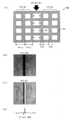
이하에, 피검사체로서의 포토마스크(50)의 구성에 대하여, 도면을 참조하면서 설명한다. 참조하는 도면에 있어서, 도 1은, 본 발명의 일 실시 형태에 따른 피검사체로서의 포토마스크의 구성을 예시하는 개략도이며, (a)는 포토마스크의 평면도, (b)는 포토마스크의 횡단면도를 각각 모식적으로 도시하고 있다. 또한, 도 2는, 본 발명의 일 실시 형태에 따른 피검사체로서의 포토마스크가 구비하는 반복 패턴의 구성을 모식적으로 예시하는 개략도이다.Below, the structure of the
포토마스크(50)란, 포토리소그래피 기술을 이용하여 미세 구조를 제조할 때 이용되는 노광용 마스크이다. 예를 들면, 표시 디바이스 기판용의 포토마스크의 경우에는, 도 1의 (a)에 예시한 바와 같이, 변 L1, 변 L2를 구비하는 기판으로서 구성되어 있는 경우가 많다. 전술한 바와 같이, 표시 디바이스용 기판의 제조 공정에서 이용되는 포토마스크(50)는, 변 L1 또는 변 L2가 300 mm를 초과하는 경우가 많으며, 때로는 1 m를 초과하는 대형 기판으로서 구성되는 경우도 있다. 그리고, 이러한 대형 포토마스크(50)를 이용하여 전면 노광을 행하는 데에는, 해상도보다도 광량이 우선되기 때문에, 노광용 광원으로서는, 365 nm∼436 nm의 파장을 포함하는 소정 파장 영역의 광을 발하는 광원이 이용되는 경우가 많다.The
포토마스크(50)는, 도 1의 (b)에 도시하는 바와 같이, 투명 지지체로서의 투명 기판(57)과, 투명 기판(57)의 주표면 위에 형성된 박막(차광막 혹은 반차광막)으로 이루어지는 반복 패턴(56)을 가지고 있다.As shown in FIG. 1B, the
투명 기판(57)의 재료로서는, 예를 들면 합성 석영 글래스 등이 이용된다. 또한, 반복 패턴(56)을 구성하는 박막의 재료로서는, 예를 들면 크롬 등의 차광성을 갖는 재료나, 반투광성을 갖는 재료 등이 이용된다. 또한, 박막은, 단층에 한정되지 않고 적층으로서 구성되어도 된다. 그 경우, 차광막 이외에 반투광성의 막을 수반하여도 되고, 또한, 에칭 스토퍼 등의 기능성의 막을 수반하여도 된다. 또한, 상기 박막 위에 레지스트막을 수반하여도 된다.As a material of the
표시 디바이스용의 포토마스크(50)의 반복 패턴(56)의 형상은, 예를 들면 도 2에 도시한 바와 같이, 격자 형상의 단위 패턴(53)이 주기적으로 배열된 형상으로 되어 있다. 이하, 단위 패턴(53)의 배열 주기를, 단위 패턴(53)의 피치 d로 부르 기로 한다. 또한, 단위 패턴(53)의 형상은, 격자 형상에 한정되지 않고, 라인 앤드 스페이스 형상, 사각형이나 그 밖의 형상의 단위 패턴 등, 다른 형상의 반복 패턴으로서 구성되어 있어도 된다.The shape of the repeating
(2) 포토마스크에 생긴 결함(2) Defects in the photomask
상기에 있어서, 단위 패턴(53)은 소정의 규칙에 따라 배열해야 한다. 그러나, 제조 공정 등에서의 어떠한 원인에 의해, 일부의 단위 패턴이 상기 규칙과는 서로 다른 규칙에 따라 배열되어 버리는 결함, 혹은 인접하는 복수의 단위 패턴에 생기는 결함(소위 불균일 결함)이 생기는 경우가 있다.In the above, the
본 발명에서는,이하의 결함의 검사에 있어서, 현저한 효과가 생긴다. 즉, 단위 패턴이 규칙적으로 배열되어 있는 반복 패턴을 표면에 갖는 포토마스크에서의, 상기 단위 패턴 배열의 규칙과는 서로 다른 규칙성을 가지고 복수의 상기 단위 패턴에 생기는 형상 이상 혹은 배열 이상, 또는 인접하는 복수의 상기 단위 패턴에 생기는 형상 이상 혹은 배열 이상으로서, 이상의 치수가, 상기 포토마스크가 이용되는 노광 광학계의 해상 한계 이하인 형상 이상 또는 배열 이상을 포함하는 결함이다. 특히, 노광 광학계의 해상 한계에 대하여, 1/10 이하의 결함량(단위 패턴의 위치 어긋남이나 선 폭 어긋남의 양으로서)의 경우에 유용하다.In the present invention, a remarkable effect occurs in the inspection of the following defects. That is, in a photomask having a repeating pattern on the surface of which unit patterns are regularly arranged, a shape abnormality or an array abnormality occurring in a plurality of the unit patterns having a regularity different from the rule of the unit pattern arrangement, or adjacent to each other. As a shape abnormality or an array abnormality which generate | occur | produces in the said some unit pattern mentioned above, the above dimension is a defect containing the shape abnormality or an array abnormality which is below the resolution limit of the exposure optical system in which the said photomask is used. In particular, it is useful in the case of the defect amount (as an amount of position shift or line width shift of a unit pattern) of 1/10 or less with respect to the resolution limit of an exposure optical system.
이하에, 반복 패턴(56)에 생기는 결함에 대하여, 포토마스크(50)의 제조 방법을 들어 설명한다. 또한, 전술한 바와 같이, 라인 앤드 스페이스 형상의 단위 패턴에서의 선 폭 이상이나 위치 어긋남도, 본 실시 형태의 검사 대상으로 하는 결함에 포함된다.Below, the defect which arises in the repeating
포토마스크(50)의 제조시에는, 대부분의 경우, 이하의 [1]∼[5]의 공정이 실시된다.In manufacturing the
[1] 우선, 투명 기판(57) 위에 박막(차광막 등)을 형성하고, 또한, 이 박막 위에 레지스트막을 형성한다.[1] First, a thin film (light shielding film or the like) is formed on the
[2] 다음으로, 형성한 레지스트막에, 묘화기를 이용하여, 예를 들면 래스터 묘화 방법 등의 묘화 방법에 의해 레이저광 등을 조사하여, 소정의 패턴을 노광한다.[2] Next, the formed resist film is irradiated with a laser beam or the like by a drawing method such as a raster drawing method by using a drawing machine to expose a predetermined pattern.
[3] 다음으로 현상을 행하여, 묘화부 또는 비묘화부의 레지스트막을 선택적으로 제거하여, 박막 위에 레지스트 패턴을 형성한다.[3] Next, development is performed to selectively remove the resist film of the drawing portion or the non-drawing portion, thereby forming a resist pattern on the thin film.
[4] 그 후, 레지스트 패턴에 덮혀져 있지 않은 박막을 에칭에 의해 선택적으로 제거하여, 반복 패턴(56)을 형성한다.[4] After that, the thin film not covered with the resist pattern is selectively removed by etching to form a repeating
[5] 계속하여, 반복 패턴(56) 위의 잔존 레지스트를 제거한다. 또한, 다층막의 경우에는, 막의 재료에 따른 추가 공정을 설정할 수 있다.[5] Subsequently, the remaining resist on the repeating
여기에서, 전술한 [2]의 공정에 있어서, 레이저광의 주사 정밀도가 갑자기 악화되거나, 또는 빔 직경이 갑자기 변동되거나, 또는 환경 요인이 변동되거나 하는 것 등에 의해, 반복 패턴(56)에 결함이 발생하는 경우가 있다. 또한, 전술한 [3], [4]의 공정에 있어서, 현상이나 에칭에 면내 불균일이 생기면, 임의의 영역에서는, 인접하는 복수의 단위 패턴에, 동시에, 형상 이상이나 배열 이상이 생기는 경우가 있다. 도 5는, 반복 패턴에 생긴, 서로 다른 규칙성을 갖는 결함을 예시하는 개략도이며, (a) 및 (b)는 좌표 위치 변동계의 결함을, (c) 및 (d)는 치수 변동 계의 결함을 각각 예시하고 있다. 또한, 도 5에 있어서는, 결함이 생긴 개소를 부호 54로 나타내고 있다.Here, in the above-described step [2], a defect occurs in the repeating
예를 들면, 도 5의 (a)는, 레이저광에 의한 묘화의 이음매에 위치 어긋남이 발생한 것에 의해, 단위 패턴(53)의 피치 d가 부분적으로 넓어지게 된 결함을 나타낸다. 또한, 도 5의 (b)는, 레이저광에 의한 묘화의 이음매에 위치 어긋남이 발생한 것에 의해, 단위 패턴(53')의 위치가 다른 단위 패턴(53)에 대하여 상대적으로 어긋나게 된 결함을 나타낸다. 이들 결함은 좌표 위치 변동계의 결함이라고 칭할 수 있다.For example, FIG. 5 (a) shows a defect in which the pitch d of the
또한, 도 5의 (c) 및 도 5의 (d)는, 묘화기의 빔 강도나 빔 직경이 변동한 것 등에 의해, 단위 패턴(53')의 크기, 즉 격자틀(53a')의 폭이 변동하게 된 결함을 나타낸다. 이들 결함은 치수 변동계의 결함이라고 칭할 수 있다.5C and 5D show the size of the unit pattern 53 ', that is, the width of the
또한, 이러한 결함의 발생 원인은, 반드시 상기에 한정되지 않고, 그 밖의 다양한 원인에 의해 생기는 경우가 있다. 단, 이 결함의 특징은, 영상 디바이스(표시 디바이스나 촬상 디바이스)의 제조에 이용되는 패턴 내에 생기기 때문에, 대부분의 경우, 마스크 사용시에 이용하는 노광기의 해상 한계 이하의 결함량(위치 어긋남량, 치수 변동량)이며, 디바이스의 동작에 이상을 초래하는 것이 아님에도 불구하고, 결함으로서, 정상 패턴과 식별할 필요가 있다.In addition, the cause of generation of such a defect is not necessarily limited to the above, and may be caused by various other causes. However, since the characteristic of this defect arises in the pattern used for manufacture of an imaging device (display device or imaging device), in most cases, the amount of defects (position shift amount, dimensional variation amount) below the resolution limit of the exposure machine used at the time of use of a mask. Although it does not cause abnormality in the operation of the device, it is necessary to identify it as a normal pattern as a defect.
(3) 패턴 결함 검사 장치의 구성(3) Configuration of pattern defect inspection apparatus
계속하여, 본 발명의 일 실시 형태에 따른 패턴 결함 검사 장치(10)의 구성예에 대하여, 도 3을 참조하면서 설명한다. 패턴 결함 검사 장치(10)는, 유지 수 단으로서의 스테이지(11)와, 조명 수단으로서의 광원 장치(12)와, 수광 수단으로서의 촬상 장치(14)와, 해석 수단으로서의 화상 해석 장치(16)를 가지고 있다.Next, the structural example of the pattern
[스테이지][stage]
유지 수단으로서의 스테이지(11)는, 피검사체로서의 포토마스크(50)를 유지하도록 구성되어 있다.The
스테이지(11)는, 반복 패턴(56)의 주평면에 대하여 비스듬하게 아래쪽으로부터 광을 조사할 수 있도록, 포토마스크(50)를 유지한다. 예를 들면, 스테이지(11)는, 포토마스크(50)의 외주부를 유지하는 틀 모양의 형상으로서 구성되어 있어도 되고, 조사하는 광에 대하여 투명한 부재에 의해 구성되어 있어도 된다.The
또한, 스테이지(11)는, 예를 들면 X방향 및 Y방향으로 이동 가능한 X-Y 스테이지로서 구성되어 있다. 그리고, 스테이지(11) 위에 유지되는 포토마스크(50)를, 후술하는 광원 장치(12) 및 촬상 장치(14)에 대하여 상대적으로 이동시킴으로써, 검사 시야를 이동시킬 수 있도록 구성되어 있다. 또한, 스테이지(11)를 이동 가능하게 구성하지 않는 경우에는, 광원 장치(12) 및 촬상 장치(14)를 스테이지(11)에 대하여 이동 가능하게 구성하여도 된다. 이 경우, 광원 장치(12) 및 촬상 장치를 동기하여 피검사체에 대하여 이동시키는 것이 가능하다. 이 때, 피검사체에 대하여 광원 장치(12)와 촬상 장치(14)를 동일한 측에 배치하여 일체로 구성하고, 또한 피검사체로부터의 반사광을 수광하는 장치 구성으로 하는 것이 유리하다. 이와 같이 구성하면, 광원 장치(12)와 촬상 장치(14)를 광축의 어긋남을 방지하면서 동기하여 이동시키는 것이 용이해지기 때문이다.In addition, the
[광원 장치][Light source device]
조명 수단으로서의 광원 장치(12)는, 스테이지(11)에 유지된 포토마스크(50)의 반복 패턴(56)에, 소정의 입사각으로 광을 조사하여, 회절광을 발생시키도록 구성되어 있다.The
광원 장치(12)는, 충분한 휘도(예를 들면, 조도가 1만 Lx∼60만 Lx 이상, 바람직하게는 30만 Lx 이상)를 가지며, 평행성이 높은(평행도가 2°이내인) 광원(12a)을 이용하는 것이 바람직하다. 그리고, 광원 장치(12)로부터의 광의 파장 λ는, 전술한 휘도를 저렴하게 얻기 위하여, 또한 후술하는 촬상 장치(14)를 저렴하게 실현하기 위하여, 파장 380 nm∼780 nm(가시광역)로 하는 것이 바람직하다. 이러한 조건을 만족할 수 있는 광원(12a)으로서는, 예를 들면 초고압 수은 램프, 크세논 램프, 메탈 할라이드 램프 등을 들 수 있다.The
광원 장치(12)는, 렌즈를 포함하는 조사 광학계(12b)를 구비하고 있다. 조사 광학계(12b)는, 스테이지(11)의 지지면(즉 반복 패턴(56)의 주평면)과 광원(12a) 사이에 배치되고, 광원(12a)으로부터의 광을 평행화하도록 구성되어 있다.The
조사 광학계(12b)에 의해 평행화된 광은, 반복 패턴(56)의 주평면을 비스듬하게 아래쪽으로부터 입사각 θi로 조사하여, 회절광을 발생시킨다. 또한, 여기서 말하는 입사각 θi란, 스테이지(11)의 지지면의 법선과, 조사광의 광축 사이에 끼워지는 각도를 말한다. 또한, 도 1에 있어서, 광원 장치(12)는, 스테이지(11)의 지지면에 대하여 비스듬하게 아래쪽에 배치되고, 후술하는 수광 수단은, 반복 패턴으로부터의 투과광을 수광하고 있지만, 스테이지(11)의 지지면에 대하여 비스듬하 게 위쪽에 배치되어 있어도 된다. 그 경우, 수광 수단은, 반복 패턴이 발생하는 반사광을 수광하게 된다. 또한, 반사광을 이용하는 방법에 의하면, 피검사체로서 투명 이외의 기판 위에 패턴을 형성한 것도 적용할 수 있다. 또한, 전술한 바와 같이, 반사광을 이용하는 방법은, 조사 광학계와 촬상 장치를, 피검사체에 대하여 동일한 측에 설치할 수 있기 때문에, 일체로 구성하는 것이 가능해져, 검사시의 광축을 안정하게 유지하는 측면에서 유리하다. 또한, 반사광을 이용하는 방법에서는, 투과광을 수광하는 경우와 비교하여, 수광 광량이 크고(기판에 의한 광의 흡수에 의한 감쇠를 감안할 필요가 없음), 광학계의 각도의 제어가 용이(기판의 두께에 의한 굴절의 영향을 감안할 필요가 없음)하다는 점에서, 검사 정밀도상의 이점이 있다.The light parallelized by the irradiation
또한, 입사각 θi는 30°내지 60°로 하는 것이 바람직하다. 입사각 θi를 지나치게 크게 하면, 후술하는 촬상 장치(14)에서 수광되는 회절광의 차수의 절대치가 커지고, 회절광의 광량이 감소하여, 결함의 검출이 곤란해지기 때문이다. 또한, 전술한 바와 같이 반복 패턴(56)은 투명 기판(57) 위에 형성되어 있지만, 입사각 θi를 지나치게 크게 하면, 피검사 영역 내에 균일한 조도로 광을 조사하는 것이 곤란해져, 바람직하지 않다. 한편, 입사각 θi를 지나치게 작게 하면, 촬상 장치(14)에서 반복 패턴(56)을 투과한 투과광이 수광되어, 강도가 높은 투과광(제로차 광)에 결함의 신호를 포함하는 회절광이 묻혀지게 되어, 결함의 검출이 곤란해지기 때문이다.In addition, it is preferable that incident angle (theta) i shall be 30 degrees-60 degrees. This is because if the incident angle θi is made too large, the absolute value of the order of the diffracted light received by the
[촬상 장치][Imaging device]
수광 수단으로서의 촬상 장치(14)는, 반복 패턴(56)으로부터의 회절광을 수광하여, 결상시키도록 구성되어 있다.The
촬상 장치(14)는, 예를 들면 CCD 카메라 등의 2차원의 화상을 촬영할 수 있는 에리어 카메라(14a)를 가지고 있다. 에리어 카메라(14a)의 수광면은, 스테이지(11)의 지지면(즉, 반복 패턴(56)의 주평면)과 대향하도록 형성되어 있다.The
촬상 장치(14)는, 대물 렌즈를 갖는 수광 광학계(14b)를 더 가지고 있다. 수광 광학계(14b)는, 반복 패턴(56)으로부터 소정의 차수의 회절광을 수광하여, 에리어 카메라(14a)의 수광면 위에 결상시킨다. 또한, 도 4에 도시한 바와 같이, 수광 광학계(14b)는 회절광을 집광하는 대물 렌즈(14c)와, 조리개(14d)를 가지고 있다. 그리고, 대물 렌즈(14c)의 개구 NA는, 대물 조리개(14d)에 의해, 파장 λ/피치 d보다도 작아지도록 구성되어 있다. 또한, 수광 광학계(14b)를 통한 촬상 장치(14)의 시야는, 예를 들면 한 변이 10 mm∼50 mm인 정방형 혹은 사각 형상으로 되도록 구성되어 있다.The
촬상 장치(14)는, 스테이지(11)의 지지면에 대하여 위쪽에 배치되어 있고, 수광각 θr로 회절광을 수광한다. 여기서 수광각 θr이란, 스테이지(11)의 지지면(즉, 반복 패턴(56)의 주평면)과, 수광 광학계(14b)의 광축 사이에 끼워지는 각도를 말한다. 또한, 수광각 θr은 실질적으로 90°로 하는 것이 바람직하다. 촬상 장치(14)가 스테이지(11)의 지지면의 법선 위에 배치되어 있는 경우에는, 촬상 장치(14)가 스테이지(11)의 지지면에 대하여 경사 방향으로 배치되어 있는 경우와 비교하여, 왜곡(에리어 카메라(14a)의 수광면으로부터 먼 쪽이 상이 작아짐과 함 께, 가까운 쪽이 상이 커져, 상이 사다리꼴 형상으로 되어 버리는 왜곡)이 생기기 어려워지기 때문이다. 즉, 동일한 검사 시야 내에 있어서, 균일한 상을 얻기 쉬워지기 때문이다.The
또한, 에리어 카메라(14a)의 수광면 위에 결상된 회절광의 상(이하, 에리어 화상이라고 함)은, 화상 데이터로서, 화상 해석 장치(16)에 출력하는 것이 가능하도록 구성되어 있다.The diffraction light image (hereinafter referred to as an area image) formed on the light receiving surface of the
[화상 해석 장치][Image analysis device]
해석 수단으로서의 화상 해석 장치(16)는, 촬상 장치(14)로부터 출력된 에리어 화상을 관찰하여, 에리어 화상 내에서의 광 강도 분포의 이변을 검출함으로써, 반복 패턴(56)에 생긴 결함의 유무를 검출할 수 있도록 구성되어 있다. 또한, 광 강도 분포의 이변을 검출함으로써 결함을 검출할 수 있는 이유에 대해서는, (4) 패턴 결함 검사 방법의 항에서 후술한다.The
즉, 화상 해석 장치(16)는, 촬상 장치(14)로부터 에리어 화상의 화상 데이터를 수신한 후, 에리어 화상에서의 광 강도 분포를 수치화한 수치 데이터를 작성하도록 구성되어 있다. 그리고, 화상 해석 장치(16)는, 이러한 수치 데이터와, 결함이 없는 경우의 에리어 화상에 기초한 수치 데이터(기준 데이터)를 정량적으로 비교함으로써, 광 강도 분포의 이변을 객관적으로 검출하도록 구성되어 있다.That is, the
또한, 화상 해석 장치(16)는, 에리어 화상의 화상 데이터를 수신한 후, 에리어 화상을 미분하여 광 강도 변화율의 분포를 나타내는 미분 화상을 작성함과 함께, 광 강도 변화율의 분포를 수치화한 수치 데이터를 작성하도록 구성되어 있다.Furthermore, after receiving the image data of the area image, the
그리고, 화상 해석 장치(16)는, 이러한 수치 데이터와, 결함이 없는 경우의 에리어 화상을 미분하여 얻은 수치 데이터(기준 데이터)를 정량적으로 비교함으로써, 광 강도 분포의 이변의 검출 감도를 향상시키도록 구성되어 있다.Then, the
(4) 패턴 결함 검사 방법(4) pattern defect inspection method
계속하여, 본 발명의 일 실시 형태에 따른 패턴 결함 검사 방법에 대하여 설명한다. 본 패턴 결함 검사 방법은, 전술한 패턴 결함 검사 장치에 의해 실시된다.Subsequently, the pattern defect inspection method according to the embodiment of the present invention will be described. This pattern defect inspection method is performed by the pattern defect inspection apparatus described above.
본 패턴 결함 검사 방법은, 반복 패턴(56)에 소정의 입사각으로 광을 조사하여 회절광을 생기게 하는 공정(S1)과, 반복 패턴(56)으로부터의 회절광을 수광하여 결상시키는 공정(S2)과, 회절광을 결상시킨 상을 관찰함으로써, 반복 패턴(56)에 생긴 결함의 유무를 검출하는 공정(S3)을 갖고 있다. 이하, 각 공정에 대하여 순서대로 설명한다.The pattern defect inspection method includes a step (S1) of irradiating light to a repeating
[회절광을 생기게 하는 공정(S1)][Process of producing diffraction light (S1)]
우선, 반복 패턴(56)을 구비한 포토마스크(50)를, 패턴 검사 장치의 스테이지(11) 위에 유지한다. 그리고, 광원 장치(12)를 이용하여, 반복 패턴(56)의 주평면에 대하여 비스듬하게 아래쪽으로부터 입사각 θi로 광을 조사한다.First, the
그러면, 반복 패턴(56)의 투과광측 및 반사광측에, 회절광이 발생한다. 그리고, 단위 패턴(53)의 피치가 d이고, 광원 장치(12)로부터 입사하는 광의 파장이 λ이고, 입사각이 θi일 때에는, d(sinθi±sinθn)=nλ의 관계를 충족시키도록 하는 회절각 θn의 방향으로, n차의 회절광이 관측된다.Then, diffracted light is generated on the transmitted light side and the reflected light side of the repeating
도 4는, 반복 패턴(56)에 입사각 θi로 광을 조사하고, 수광각 90°로 회절광을 수광하는 상태를 나타내는 개략도이며, (a)는 단위 패턴의 피치 d가 10 ㎛인 경우에서의 회절광의 상태를 나타내고, (b)는 이러한 경우에서의 회절광의 차수와 입사각의 관계를 나타내고 있다. 또한,(c)는 단위 패턴의 피치 d가 1 ㎛인 경우에서의 회절광의 상태를 나타내고, (d)는 이러한 경우에서의 회절광의 차수와 입사각의 관계를 나타내고 있다. 도 4에 의하면, 단위 패턴(53)의 피치 d가 클수록, 인접하는 회절광끼리의 회절각의 차 Δθ(즉, θn±1과 θn의 차)가 작아지는 것을 알 수 있다.4 is a schematic diagram showing a state in which light is irradiated to the repeating
[회절광을 수광하여 결상시키는 공정(S2)][Step of Receiving and Image Forming Diffracted Light (S2)]
계속하여, 촬상 장치(14)에 의해, 반복 패턴(56)으로부터의 회절광을 수광하여 결상시킨다. 즉, 수광 광학계(14b)에 의해, 반복 패턴(56)으로부터의 회절광을 수광시키고, 에리어 카메라(14a)의 수광면 위에 결상시켜 에리어 화상을 얻는다.Subsequently, the
여기에서, 결함이 없는 반복 패턴(56)에 있어서는, 각 단위 패턴(53)의 피치 d는 균일하기 때문에, 파장 λ, 입사각 θi, 회절각 θn이 동일한 한, 특정한 차수의 회절광을 결상시킨 상은, 일정한 규칙성을 가진 것으로 될 것이다. 이에 대하여, 결함이 생긴 반복 패턴(56')의 피치 d'는, 결함이 없는 반복 패턴(56)의 피치 d와는 다르다. 그 때문에, 파장 λ, 입사각 θi, 회절각 θn이 동일한 경우에는, 결함이 생긴 반복 패턴(56')에 의한 에리어 화상과, 결함이 없는 반복 패턴(56)에 의한 에리어 화상은, 어떠한 상위가 생기게 된다. 구체적으로는, 전자의 에리어 화상 내에는, 결함에 기인하는 광 강도 분포의 이변이 나타나게 된다. 그리고, 이 광 강도 분포의 이변은, 후자의 에리어 화상에는 나타나지 않는다.Here, in the repeating
그 후, 촬상 장치(14)는, 에리어 화상의 화상 데이터를, 화상 해석 장치(16)에 출력한다.Thereafter, the
또한, 상기에 있어서는, 반복 패턴(56)의 비스듬하게 아래쪽으로부터 광을 조사하여 투과면에서 회절광을 수광하는 경우를 예로 들어 설명했지만, 반복 패턴(56)의 비스듬하게 위쪽에서부터 광을 조사하여, 반사면에서 회절광을 수광하는 경우에 대해서도, 마찬가지의 결과를 얻을 수 있다.In addition, in the above, the case where light was irradiated from obliquely downward of the repeating
[결함의 유무를 검출하는 공정(S3)][Step (S3) for Detecting Presence or Absence of Defect]
전술한 바와 같이, 결함이 생긴 반복 패턴(56')으로부터의 에리어 화상에는, 결함의 존재를 나타내는 광 강도 분포의 이변이 나타난다. 따라서, 화상 해석 장치(16)에 의해, 에리어 화상을 관찰시켜, 반복 패턴(56)에 생긴 결함의 유무를 검사시킨다.As described above, in the area image from the repeating
구체적으로는, 화상 해석 장치(16)에, 촬상 장치(14)로부터 출력된 에리어 화상의 화상 데이터를 수신시키고, 에리어 화상의 광 강도 분포를 미분시켜 그 변화를 강조시킨 미분 화상을 작성시키고, 광 강도 분포의 변화(이변)를 관찰함으로써, 결함의 유무를 검출한다.Specifically, the
또한, 전술한 바와 같이, 입사광의 파장 λ를 380 nm∼780 nm로 하고, 입사각 θi를 30°내지 60°로 하고, 수광각 θr을 실질적으로 90°로 하는 것이 바람직하다. 그리고, 이 경우, 단위 패턴(53)의 피치 d는 1 ㎛∼8 ㎛로 하는 것이 바람직하다. 이때, 상기 에리어 화상, 또는 그 미분 화상을 관찰하면, 결함에 기인 하는 신호가, 원래의 반복 패턴(결함이 없는 반복 패턴)에 기인하는 신호에 대하여, SN비 1.2 이상으로 명확하게 구별하는 것이 가능하다. 또한, 전술한 d(sinθn±sinθi)=nλ라는 관계식에 의하면, 파장 λ, 입사각 θi, 수광각 θr, 피치 d가 전술한 조건이면, 촬상 장치(14)에서, 차수의 절대치가 1∼10인 회절광을 수광할 수 있다. 차수의 절대치가 1∼10인 회절광은 광량이 많아, 밝은 에리어 화상을 얻을 수 있고, 결함의 존재를 나타내는 광 강도 분포의 변동(이변)을 신뢰성 좋게 검출하는 것이 가능하다.As described above, it is preferable that the wavelength? Of the incident light is 380 nm to 780 nm, the incident angle θi is set to 30 ° to 60 °, and the light receiving angle θr is set to substantially 90 °. In this case, the pitch d of the
(5) 본 실시 형태에서의 효과(5) Effect in this embodiment
본 실시 형태에 의하면, 이하의 [1]∼[4]의 효과를 발휘한다.According to this embodiment, the effect of the following [1]-[4] is exhibited.
[1] 본 실시 형태에 의하면, 반복 패턴(56)에 생긴 미세한 결함은, 에리어 화상 내에 광 강도 분포의 이변으로서 명료하게 나타난다. 따라서, 각 단위 패턴(53)의 치수나 좌표를 개별적으로 측정하는 검사(마이크로 검사)를 실시하지 않아도, 에리어 화상 내에서의 광 강도 분포의 이변을 관찰함으로써, 반복 패턴(56)의 결함을 검사하는 것이 가능하게 된다. 그리고, 이러한 검사를, 복수의 단위 패턴(53)을 포함하는 매크로 영역(즉 한 변이 10 mm∼50 mm인 정방형 혹은 사각 형상의 검사 시야)에 대하여 행하면, 포토마스크(50)의 검사 시간을 단축할 수 있어, 생산성을 향상시키는 것이 가능하게 된다.[1] According to the present embodiment, the minute defects generated in the repeating
예를 들면, 하이비젼 TV용의 표시 디바이스용 기판(42V형, 면적 약 0.5 m2)의 제조에 이용되는 포토마스크(50)는, 1920(수직)×1080(수평)=2,073,600개의 단 위 패턴(53)을 가지고 있다. 여기에서, 모든 단위 패턴(53)의 치수나 좌표를, 레이저 길이 측정기나 현미경 등을 이용하여 마이크로 검사하고자 하면, 단위 패턴 1개당의 측정 소요 시간을 약 10초로 한 경우에, 약 240일이 필요하게 된다. 이에 대하여, 본 실시 형태에 의하면, 예를 들면 매크로 검사의 시야가 한 변 25 mm(단, 인접 시야와의 중복을 1할 예상함)이고, 하나의 시야에서의 검사 시간(즉, 상기의 S1∼S3까지의 실행 시간)이 2.5초 정도인 것으로 하면, 40분 남짓의 검사 시간으로 검사를 완료시키는 것이 가능하게 된다. 즉, 포토마스크(50)의 검사 시간을 대폭 단축시켜, 포토마스크(50)의 생산성을 대폭 향상시키는 것이 가능하게 된다.For example, the
[2] 본 실시 형태에 의하면, 입사광의 파장 λ가 380 nm∼780 nm이고, 입사각 θi가 30°내지 60°이고, 수광각 θr이 실질적으로 90°인 경우에 있어서, 단위 패턴(53)의 피치 d를 1 ㎛∼8 ㎛로 함으로써, 촬상 장치(14)에서, 결함에 유래하는 광 강도의 이변을 명료하게 관찰할 수 있다. 이 때, 차수의 절대치가 1∼10인 회절광을 수광할 수 있는데, 차수의 절대치가 1∼10인 회절광은 광량이 많아, 밝은 에리어 화상을 얻을 수 있기 때문에, 결함의 존재를 나타내는 광 강도 분포의 변동(이변)을 신뢰성 좋게 검출하는 것이 가능하게 된다.[2] According to the present embodiment, in the case where the wavelength λ of incident light is 380 nm to 780 nm, the incident angle θi is 30 ° to 60 °, and the light receiving angle θr is substantially 90 °, the
[3] 본 실시 형태에 의하면, 화상 해석 장치(16)는, 에리어 화상에서의 광 강도 분포를 수치화한 수치 데이터와, 결함이 없는 경우의 에리어 화상에 기초한 수치 데이터를 정량적으로 비교함으로써, 광 강도 분포의 이변(결함)을 검출한다. 즉, 광 강도 분포를 수치화하여 정량적으로 해석함으로써, 결함의 유무를, 육안 관찰에 의한 작업자의 인상에 의존하지 않고 객관적으로 검출하는 것이 가능하게 된 다. 이에 의해, 검사 결과의 변동을 억제시켜, 검사의 신뢰성을 향상시키는 것이 가능하게 된다.[3] According to the present embodiment, the
[4] 본 실시 형태에 의하면, 에리어 화상을 미분하여 광 강도 분포의 변화를 강조시킨 미분 화상을 작성하고, 이 미분 화상에서의 광 강도 변화 분포를 수치화한 수치 데이터와, 결함이 없는 경우의 에리어 화상을 미분하여 얻은 수치 데이터를 정량적으로 비교함으로써, 광 강도 분포의 이변(결함)의 검출 감도를 더욱 향상시키는 것이 가능하게 된다.[4] According to the present embodiment, a differential image is obtained by differentiating an area image to emphasize the change in the light intensity distribution, and numerical data obtained by quantifying the light intensity change distribution in the differential image, and the area in which there is no defect. By quantitatively comparing numerical data obtained by differentiating an image, it becomes possible to further improve the detection sensitivity of aberrations (defects) in the light intensity distribution.
<B> 본 발명의 다른 실시 형태<B> Other Embodiments of the Invention
계속하여, 본 발명의 다른 실시 형태를 설명한다.Subsequently, another embodiment of the present invention will be described.
전술한 바와 같이, 입사광의 파장 λ를 380 nm∼780 nm로 하고, 입사각 θi를 30°내지 60°로 하고, 수광각 θr을 실질적으로 90°로 하는 것이 바람직하다. 그리고, 이 경우에는, 단위 패턴(53)의 피치 d를 1 ㎛∼8 ㎛로 함으로써, 결함에 기인하는 정보와, 결함이 없는 반복 패턴에 기인하는 정보를 명확하게 구별하는 것이 가능하게 된다. 그러나, 단위 패턴(53)의 피치 d는, 피검사체의 용도나 사양 등에 의해 정해지는 것이며, 실제로는 단위 패턴(53)의 피치 d가 8 ㎛를 초과하는 경우가 있다.As described above, it is preferable that the wavelength λ of the incident light is 380 nm to 780 nm, the incident angle θi is 30 ° to 60 °, and the light receiving angle θr is substantially 90 °. In this case, by setting the pitch d of the
여기에서, 단위 패턴(53)의 피치 d가 큰 경우에는, 인접하는 회절광끼리의 회절각의 차 Δθ가 작아진다. 그 때문에, 파장 λ, 입사각 θi, 수광각 θr, 피치 d가 전술한 조건인 경우에는, 촬상 장치(14)에서 수광되는 회절광의 차수의 절대치는, 1∼10보다도 훨씬 커지게 된다. 이러한 고차 회절광은 광량이 적기 때문 에, 에리어 화상은 어두워지고, 결함의 존재를 나타내는 광 강도 분포의 변동(이변)을 신뢰성 좋게 검출하는 것이 곤란한 경우가 있다.Here, in the case where the pitch d of the
그러나, 단위 패턴(53)의 피치 d가 8 ㎛를 초과하는 경우에 있어서는, 단위 패턴(53)과는 서로 다른 피치로 테스트용 단위 패턴이 주기적으로 배열된 테스트용 패턴(56t)을, 반복 패턴(56) 이외의 영역에 반복 패턴(56)과 동시에 묘화함으로써 형성함과 함께, 테스트용 단위 패턴(53t)의 피치 d를 1 ㎛∼8 ㎛로 함으로써, 전술한 문제를 해결할 수 있다. 또한, 본 발명의 테스트용 패턴의 피치는, 1 ㎛ 미만이라도 상관없지만, 테스트 패턴의 묘화 정밀도를 확보하는 목적, 및 묘화 데이터가 과대한 용량으로 되는 것을 방지하는 목적으로부터, 1 ㎛ 이상인 것이 바람직하다. 특히, 후자에 대하여 말하자면, 본 발명의 피검사체는, 한 변이 300 mm 이상, 보다 효과가 높은 것은 한 변이 1 m 이상인 대형의 것이기 때문에, 묘화 용량을 억제하는 것은 의의가 크다.However, in the case where the pitch d of the
이하에, 본 실시 형태에 따른 (1) 피검사체로서의 포토마스크의 구성, (2) 패턴 결함 검사 장치의 구성, (3) 본 실시 형태에 따른 패턴 결함 검사 방법을 순서대로 설명한다.Below, (1) the structure of the photomask as a to-be-tested object concerning this embodiment, (2) the structure of a pattern defect inspection apparatus, and (3) the pattern defect inspection method which concerns on this embodiment are demonstrated in order.
(1) 포토마스크의 구성(1) Composition of photo mask
본 실시 형태에 따른 피검사체로서의 포토마스크는, 도 8에 도시한 바와 같이, 투명 지지체로서의 투명 기판(57)의 주표면 위에, 반복 패턴(56)과 동시에 형성된 박막(차광막)으로 이루어지는 테스트용 패턴(56t)을 가지고 있는 점이, 전술한 실시 형태와 다르다. 테스트용 패턴(56t)은, 반복 패턴(56) 이외의 영역, 예를 들면 투명 기판(57)의 주표면 위에서의 반복 패턴(56)의 주위 등에 형성되어 있다.As shown in FIG. 8, the photomask as a test object which concerns on this embodiment consists of a test pattern which consists of a thin film (light shielding film) formed simultaneously with the repeating
또한, 테스트용 패턴(56t)의 형상은, 예를 들면 격자 형상의 테스트용 단위 패턴(53t)이 주기적으로 배열된 형상으로 되어 있다. 여기에서, 테스트용 단위 패턴(53t)의 피치 d는, 단위 패턴(53)의 피치 d와는 독립적으로 정하는 것이 가능하며, 예를 들면 1 ㎛∼8 ㎛로 되도록 구성되어 있다. 또한, 테스트용 패턴(56t)의 형상은, 격자 형상에 한정되지 않고, 라인 앤드 스페이스 형상 등, 다른 형상의 반복 패턴으로서 구성되어 있어도 된다.The
여기에서, 테스트용 패턴(56t)의 묘화는, 반복 패턴(56)의 묘화와 동시에 행해진다. 즉, 투명 기판(57) 위에 형성한 레지스트막에 대하여, 동일한 묘화기를 이용하여, 테스트용 패턴(56t)과 반복 패턴(56)을 연속적으로 묘화한다. 따라서, 묘화기의 주사 이상 등에 의해 반복 패턴(56)에 결함이 발생하는 경우에는, 테스트용 패턴(56t)에도 마찬가지의 결함이 생기게 된다.Here, drawing of the
그 밖의 구성은, 전술한 실시 형태에 따른 포토마스크와 동일하다.The other structure is the same as that of the photomask which concerns on embodiment mentioned above.
(2) 패턴 결함 검사 장치의 구성(2) Configuration of pattern defect inspection apparatus
계속하여, 본 발명의 다른 실시 형태에 따른 패턴 결함 검사 장치(10)의 구성예에 대하여 설명한다.Next, the structural example of the pattern
본 실시 형태에 따른 조명 수단으로서의 광원 장치(12)는, 스테이지(11)에 유지된 포토마스크(50)의 테스트용 패턴(56t)에, 소정의 입사각으로 광을 조사하여 회절광을 발생시키도록 구성되어 있는 점이, 전술한 실시 형태에 따른 패턴 결함 검사 장치(10)와 다르다. 또한, 본 실시 형태에 따른 수광 수단으로서의 촬상 장 치(14)는, 테스트용 패턴(56t)으로부터의 회절광을 수광하여, 결상시키도록 구성되어 있는 점이, 전술한 실시 형태에 따른 패턴 결함 검사 장치(10)와 다르다. 또한, 본 실시 형태에 따른 해석 수단으로서의 화상 해석 장치(16)는, 테스트용 패턴(56t)으로부터의 회절광을 결상시킨 상(촬상 장치(14)가 수광하여 결상시킨 에리어 화상)을 관찰함으로써, 반복 패턴(56)에 생긴 결함의 유무를, 간접적으로 검출할 수 있도록 구성되어 있는 점이, 전술한 실시 형태에 따른 패턴 결함 검사 장치(10)와 다르다.The
그 밖의 구성은, 전술한 실시 형태에 따른 패턴 결함 검사 장치(10)와 동일하다.The other structure is the same as that of the pattern
(3) 패턴 결함 검사 방법(3) pattern defect inspection method
계속하여, 본 발명의 일 실시 형태에 따른 패턴 결함 검사 방법에 대하여 설명한다. 본 패턴 결함 검사 방법은, 전술한 패턴 결함 검사 장치에 의해 실시된다.Subsequently, the pattern defect inspection method according to the embodiment of the present invention will be described. This pattern defect inspection method is performed by the pattern defect inspection apparatus described above.
우선, 전술한 테스트용 패턴(56t)을, 반복 패턴(56) 이외의 영역에 반복 패턴(56)과 동시에 묘화하여 형성한다.First, the
계속하여, 반복 패턴(56) 및 테스트용 패턴(56t)을 구비한 포토마스크(50)를, 패턴 검사 장치의 스테이지(11) 위에 유지한다. 그리고, 광원 장치(12)를 이용하여, 테스트용 패턴(56t)의 주평면에, 비스듬하게 아래쪽으로부터 입사각 θi로 광을 조사한다.Then, the
계속하여, 촬상 장치(14)를 이용하여, 테스트용 패턴(56t)으로부터의 회절광 을 수광하여 결상시킨다. 즉, 수광 광학계(14b)에 의해, 테스트용 패턴(56t)으로부터의 회절광을 수광시키고, 에리어 카메라(14a)의 수광면 위에 결상시켜, 에리어 화상을 얻는다.Subsequently, the
계속하여, 화상 해석 장치(16)에, 테스트용 패턴(56t)의 에리어 화상의 화상 데이터를 수신시키고, 에리어 화상의 광 강도 분포를 미분시켜 그 변화를 강조시킨 미분 화상을 작성시키고, 광 강도 분포의 변화(이변)를 관찰함으로써, 반복 패턴(56)에 생긴 결함의 유무를 검출한다.Subsequently, the
그 밖의 구성은, 전술한 실시 형태에 따른 패턴 결함 검사 방법과 동일하다.The other structure is the same as the pattern defect inspection method which concerns on embodiment mentioned above.
(4) 본 실시 형태에서의 효과(4) Effect in this embodiment
본 실시 형태에 의하면, 전술한 본 발명의 일 실시 형태에서의 [1]∼[4]의 효과 외에, 또한 이하의 효과를 발휘한다.According to this embodiment, in addition to the effects of [1] to [4] in one embodiment of the present invention described above, the following effects are further exhibited.
[5] 본 실시 형태에 의하면, 단위 패턴(53)의 피치 d가 8 ㎛를 초과하는 경우이어도, 회절광을 이용하여 반복 패턴(56)에 생긴 결함을 단시간에 신뢰성 좋게 검출할 수 있다. 즉, 본 실시 형태에 의하면, 단위 패턴(53)과는 서로 다른 피치로 테스트용 단위 패턴이 주기적으로 배열된 테스트용 패턴(56t)을, 반복 패턴(56) 이외의 영역에, 반복 패턴(56)과 동시에 묘화한다. 반복 패턴(56)에 결함이 생긴 경우에는, 동시에 묘화한 테스트용 패턴(56t)에도 결함이 생기기 때문에, 테스트용 패턴(56t)을 검사함으로써, 반복 패턴(56)을 간접적으로 검사하는 것이 가능하다.[5] According to the present embodiment, even when the pitch d of the
[6] 본 실시 형태에 의하면, 테스트용 단위 패턴(53t)의 피치 d는, 단위 패턴(53)의 피치 d와는 독립적으로 정하는 것이 가능하며, 1 ㎛∼8 ㎛로 할 수 있다. 그 때문에, 입사광의 파장 λ를 380 nm∼780 nm로 하고, 입사각 θi를 30°내지 60°로 하고, 수광각 θr을 실질적으로 90°로 한 경우에 있어서, 차수의 절대치가 1∼10인 회절광을 촬상 장치(14)에서 수광할 수 있다. 그 때문에, 밝은 에리어 화상을 얻을 수 있어, 결함의 존재를 나타내는 광 강도 분포의 변동(이변)을 명료하게 신뢰성 좋게 검출하는 것이 가능하게 된다.[6] According to the present embodiment, the pitch d of the test unit pattern 53t can be determined independently of the pitch d of the
<실시예><Example>
이하에, 본 발명의 실시예에 대하여, 비교예를 들어 설명한다. 참조하는 도면에 있어서, 도 7의 (a)는, 본 발명의 실시예 및 비교예에 관한 결함 검출 능력을 요약한 그래프도이며, 도 7의 (b)는 피치 d를 4 ㎛로 한 경우(실시예 1)를, 도 7의 (c)는 피치 d를 8 ㎛로 한 경우(실시예 2)를, 도 7의 (d)는 피치 d를 12 ㎛로 한 경우(비교예 1)를, 도 7의 (e)는 피치 d를 20 ㎛로 한 경우(비교예 2)에서의 광 강도 변화율의 분포를 각각 나타내는 그래프도이다.Below, the Example of this invention is given and demonstrated a comparative example. In the drawings to which reference is made, FIG. 7A is a graph summarizing defect detection capability according to Examples and Comparative Examples of the present invention, and FIG. 7B is a case where the pitch d is 4 mu m ( In Example 1), FIG. 7C shows the case where the pitch d is 8 mu m (Example 2), and FIG. 7D shows the case where the pitch d is 12 mu m (Comparative Example 1), FIG.7 (e) is a graph which shows distribution of the light intensity change rate in the case where pitch d is set to 20 micrometers (comparative example 2), respectively.
우선, 실시예 1로서, 단위 패턴(53)의 피치 d를 4 ㎛로 하고, 그 배열 중의 1열에, 의도적으로 10 nm 정도 선 폭이 큰 결함을 생기게 한 반복 패턴(56')을 구비한 포토마스크(50)를, 피검사체로서 준비하였다. 그리고, 광원 장치(12)에 의해, 파장 λ가 546 nm인 광을, 반복 패턴(56')에 대하여 입사각 θi를 45°로 하여 조사하였다. 그리고, 수광각 θr이 90°의 방향으로 설치된 촬상 장치(14)에 의해, 차수의 절대치가 5에 상당하는 회절광의 에리어 화상을 얻은 후, 미분 화상을 작성하고, 그 광 강도 변화 분포를 수치화하여 그래프에 나타내었다. 그 결과, 도 7의 (b)에 나타낸 바와 같이, 결함의 존재를 나타내는 광 강도 분포의 이변(펄스 형상의 피크)이, S/N비 좋게(1.7 이상) 확인되었다.First, as Example 1, the pitch d of the
다음으로, 실시예 2로서, 단위 패턴(53)의 피치 d를 8 ㎛로 하였다. 그리고, 반복 패턴(56')에 대하여 입사각 θi를 45°로 하여 조사하였다. 그리고, 촬상 장치(14)에 의해, 차수의 절대치가 10에 상당하는 회절광의 에리어 화상을 얻은 후, 미분 화상을 작성하고, 그 광 강도 변화 분포를 수치화하여 그래프에 나타내었다. 그 결과, 도 7의 (c)에 나타낸 바와 같이, 결함의 존재를 나타내는 광 강도 분포의 이변(펄스 형상의 피크)이, S/N비 좋게(1.5 이상) 확인되었다.Next, as Example 2, the pitch d of the
다음으로, 비교예 1로서, 단위 패턴(53)의 피치 d를 12 ㎛로 하였다. 그리고, 반복 패턴(56')에 대하여 입사각 θi를 45°로 하여 조사하였다. 그리고, 촬상 장치(14)에 의해, 차수의 절대치가 15에 상당하는 회절광의 에리어 화상을 얻은 후, 미분 화상을 작성하고, 그 광 강도 변화 분포를 수치화하여 그래프에 나타내었다. 그 결과, 도 7의 (d)에 나타낸 바와 같이, 결함의 존재를 나타내는 광 강도 분포의 이변(펄스 형상의 피크)을 S/N비 좋게 확인하는 것이 곤란하였다(S/N비 1.1 미만).Next, as the comparative example 1, the pitch d of the
다음으로, 비교예 2로서, 단위 패턴(53)의 피치 d를 20 ㎛로 하였다. 그리고, 반복 패턴(56')에 대하여 입사각 θi를 45°로 하여 조사하였다. 그리고, 촬상 장치(14)에 의해, 차수의 절대치가 25에 상당하는 회절광의 에리어 화상을 얻은 후, 미분 화상을 작성하고, 그 광 강도 변화 분포를 수치화하여 그래프에 나타내었다. 그 결과, 도 7의 (e)에 나타낸 바와 같이, 결함의 존재를 나타내는 광 강도 분포의 이변(펄스 형상의 피크)을 확인하는 것이 곤란하였다(S/N비 0.01 미만).Next, as the comparative example 2, the pitch d of the
도 1은, 본 발명의 일 실시 형태에 따른 피검사체로서의 포토마스크의 구성을 예시하는 개략도이며, (a)는 포토마스크의 평면도, (b)는 포토마스크의 횡단면도를 각각 도시하는 도면.BRIEF DESCRIPTION OF THE DRAWINGS It is a schematic diagram which shows the structure of the photomask as a to-be-tested object concerning one Embodiment of this invention, (a) is a top view of a photomask, (b) is a figure which shows the cross-sectional view of a photomask, respectively.
도 2는, 본 발명의 일 실시 형태에 따른 피검사체로서의 포토마스크가 구비하는 반복 패턴의 구성을 예시하는 개략도.2 is a schematic diagram illustrating a configuration of a repeating pattern included in a photomask as a test subject according to an embodiment of the present invention.
도 3은, 본 발명의 일 실시 형태에 따른 패턴 결함 검사 장치의 구성을 나타내는 개략도.3 is a schematic view showing the configuration of a pattern defect inspection apparatus according to an embodiment of the present invention.
도 4는, 반복 패턴에 입사각 θi로 광을 조사하고, 수광각 90°로 회절광을 수광하는 상태를 나타내는 개략도이며, (a)는 단위 패턴의 피치가 10 ㎛인 경우에서의 회절광의 상태, (b)는 피치가 10 ㎛인 경우에서의 회절광의 차수와 입사각의 관계, (c)는 단위 패턴의 피치가 1 ㎛인 경우에서의 회절광의 상태, (d)는 피치가 1 ㎛인 경우에서의 회절광의 차수와 입사각의 관계를 각각 나타내는 도면.4 is a schematic diagram showing a state in which light is irradiated to the repetitive pattern at an incident angle θi and received diffracted light at a light receiving angle of 90 °, (a) shows a state of diffracted light when the pitch of the unit pattern is 10 μm, (b) is the relationship between the order of diffracted light and the incident angle when the pitch is 10 μm, (c) is the state of the diffracted light when the pitch of the unit pattern is 1 μm, and (d) is when the pitch is 1 μm. Showing the relationship between the order of the diffracted light and the incident angle, respectively.
도 5는, 반복 패턴에 생긴 결함을 예시하는 개략도이며, (a) 및 (b)는 좌표 위치 변동계의 결함, (c) 및 (d)는 치수 변동계의 결함을 각각 예시하는 도면.5 is a schematic diagram illustrating a defect in a repeating pattern, (a) and (b) illustrating a defect in a coordinate position change system, and (c) and (d) illustrating a defect in a dimensional change system, respectively.
도 6의 (a)는 결함이 생긴 반복 패턴을 나타내고, 도 6의 (b)는 이 반복 패턴으로부터 생기는 회절광을 수광하여 결상시킨 에리어 화상을 나타내고, 도 6의 (c)는 이 에리어 화상의 광 강도를 미분하여 광 강도 분포의 변동을 강조한 미분 화상을 나타내며, 그 광 강도 변화의 변동을 나타내는 그래프도.FIG. 6 (a) shows a repeating pattern in which a defect has occurred, and FIG. 6 (b) shows an area image for receiving and imaging the diffracted light generated from this repeating pattern, and FIG. 6 (c) shows the area image of this area image. A graph showing a differential image in which the light intensity is differentiated to emphasize the variation in the light intensity distribution, and the variation in the light intensity change.
도 7의 (a)는, 본 발명의 실시예 및 비교예에 따른 결함 검출 능력을 요약한 그래프도이며, 도 7의 (b)는 피치 d를 4 ㎛로 한 경우(실시예 1), 도 7의 (c)는 피치 d를 8 ㎛로 한 경우(실시예 2), 도 7의 (d)는 피치 d를 12 ㎛로 한 경우(비교예 1), 도 7의 (e)는 피치 d를 20 ㎛로 한 경우(비교예 2)에서의 광 강도 변화율의 분포를 각각 나타내는 그래프도.FIG. 7A is a graph summarizing defect detection capabilities according to Examples and Comparative Examples of the present invention, and FIG. 7B is a case where the pitch d is 4 µm (Example 1). 7 (c) shows a pitch d of 8 占 퐉 (Example 2), and FIG. 7 (d) shows a pitch d of 12 占 퐉 (Comparative Example 1). The graph which shows distribution of the light intensity change rate in the case of making 20 micrometers (comparative example 2), respectively.
도 8은, 본 발명의 다른 실시 형태에 따른 피검사체로서의 포토마스크의 구성을 예시하는 개략도이며, (a)는 포토마스크의 평면도, (b)는 포토마스크의 횡단면도를 각각 도시하는 도면.FIG. 8 is a schematic view illustrating the configuration of a photomask as an inspection object according to another embodiment of the present invention, (a) is a plan view of the photomask, and (b) is a diagram showing a cross-sectional view of the photomask, respectively. FIG.
<도면의 주요 부분에 대한 부호의 설명><Explanation of symbols for main parts of the drawings>
10: 패턴 결함 검사 장치10: pattern defect inspection device
11: 스테이지11: stage
12a: 광원12a: light source
12b: 조사 광학계12b: irradiation optical system
12: 광원 장치12: light source device
14a: 에리어 카메라14a: area camera
14b: 수광 광학계14b: light receiving optical system
14: 촬상 장치14: imaging device
16: 화상 해석 장치16: image analysis device
50: 포토마스크50: photomask
56: 반복 패턴56: repeating pattern
57: 투명 기판57: transparent substrate
Claims (21)
Translated fromKoreanApplications Claiming Priority (2)
| Application Number | Priority Date | Filing Date | Title |
|---|---|---|---|
| JP2007092818AJP4869129B2 (en) | 2007-03-30 | 2007-03-30 | Pattern defect inspection method |
| JPJP-P-2007-00092818 | 2007-03-30 |
Publications (1)
| Publication Number | Publication Date |
|---|---|
| KR20080089251Atrue KR20080089251A (en) | 2008-10-06 |
Family
ID=39974692
Family Applications (1)
| Application Number | Title | Priority Date | Filing Date |
|---|---|---|---|
| KR1020080028923ACeasedKR20080089251A (en) | 2007-03-30 | 2008-03-28 | Pattern defect inspection method, photomask manufacturing method, and pattern transfer method |
Country Status (4)
| Country | Link |
|---|---|
| JP (1) | JP4869129B2 (en) |
| KR (1) | KR20080089251A (en) |
| CN (1) | CN101275920A (en) |
| TW (1) | TW200848694A (en) |
Cited By (3)
| Publication number | Priority date | Publication date | Assignee | Title |
|---|---|---|---|---|
| DE102008056659A1 (en) | 2007-11-09 | 2009-06-25 | Cheil Industries, Inc., Gumi | Transparent thermoplastic resin and process for its preparation |
| KR101511158B1 (en)* | 2008-12-16 | 2015-04-13 | 삼성전자주식회사 | Reticle Error Detection Method |
| US9100563B2 (en) | 2010-03-15 | 2015-08-04 | Samsung Electronics Co., Ltd. | Apparatus, method and computer-readable medium imaging through at least one aperture of each pixel of display panel |
Families Citing this family (19)
| Publication number | Priority date | Publication date | Assignee | Title |
|---|---|---|---|---|
| US7570796B2 (en) | 2005-11-18 | 2009-08-04 | Kla-Tencor Technologies Corp. | Methods and systems for utilizing design data in combination with inspection data |
| US9659670B2 (en) | 2008-07-28 | 2017-05-23 | Kla-Tencor Corp. | Computer-implemented methods, computer-readable media, and systems for classifying defects detected in a memory device area on a wafer |
| JP4596062B2 (en) | 2008-09-29 | 2010-12-08 | ブラザー工業株式会社 | Method for attaching charging wire, method for manufacturing process cartridge, and process cartridge |
| JP5178561B2 (en)* | 2009-02-06 | 2013-04-10 | Hoya株式会社 | Pattern inspection method, pattern inspection apparatus, photomask manufacturing method, and pattern transfer method |
| TW201100787A (en)* | 2009-02-18 | 2011-01-01 | Nikon Corp | Surface examining device and surface examining method |
| JP5671540B2 (en)* | 2009-09-21 | 2015-02-18 | アコーニ バイオシステムズAkonni Biosystems | Integrated cartridge |
| JP2012119512A (en)* | 2010-12-01 | 2012-06-21 | Hitachi High-Technologies Corp | Substrate quality evaluation method and apparatus therefor |
| US20120237858A1 (en)* | 2011-03-18 | 2012-09-20 | Nanya Technology Corporation | Photomask and a method for determining a pattern of a photomask |
| US9170211B2 (en) | 2011-03-25 | 2015-10-27 | Kla-Tencor Corp. | Design-based inspection using repeating structures |
| JP2013068551A (en)* | 2011-09-22 | 2013-04-18 | Toshiba Corp | Pattern checkup device and pattern checkup method |
| CN103823329B (en)* | 2012-11-16 | 2016-09-07 | 中芯国际集成电路制造(上海)有限公司 | Mask plate and the method that it is carried out defects detection |
| US9865512B2 (en) | 2013-04-08 | 2018-01-09 | Kla-Tencor Corp. | Dynamic design attributes for wafer inspection |
| US9310320B2 (en) | 2013-04-15 | 2016-04-12 | Kla-Tencor Corp. | Based sampling and binning for yield critical defects |
| TWI512772B (en)* | 2014-03-19 | 2015-12-11 | Darfon Electronics Corp | Elastic body layer and inspection method thereof |
| DE112016003230T5 (en)* | 2015-07-17 | 2018-04-19 | Toppan Printing Co., Ltd. | METAL MASK SUBSTRATE, METAL MASK SUBSTRATE CONTROL METHOD, METAL MASK AND METAL MASK MANUFACTURING METHOD |
| CN106403808A (en)* | 2015-07-29 | 2017-02-15 | 上海微电子装备有限公司 | Apparatus and method for measuring appearance of through silicon via |
| JP7292842B2 (en)* | 2018-09-21 | 2023-06-19 | キヤノン株式会社 | Foreign Matter Inspection Apparatus, Exposure Apparatus, and Article Manufacturing Method |
| JP7454331B2 (en)* | 2018-10-26 | 2024-03-22 | 株式会社トクヤマ | Fixing jig |
| JP7229138B2 (en)* | 2019-09-27 | 2023-02-27 | Hoya株式会社 | Pattern inspection method, photomask inspection apparatus, photomask manufacturing method, and display device manufacturing method |
- 2007
- 2007-03-30JPJP2007092818Apatent/JP4869129B2/ennot_activeExpired - Fee Related
- 2008
- 2008-03-20CNCNA2008100865858Apatent/CN101275920A/enactivePending
- 2008-03-28KRKR1020080028923Apatent/KR20080089251A/ennot_activeCeased
- 2008-03-28TWTW097111156Apatent/TW200848694A/enunknown
Cited By (3)
| Publication number | Priority date | Publication date | Assignee | Title |
|---|---|---|---|---|
| DE102008056659A1 (en) | 2007-11-09 | 2009-06-25 | Cheil Industries, Inc., Gumi | Transparent thermoplastic resin and process for its preparation |
| KR101511158B1 (en)* | 2008-12-16 | 2015-04-13 | 삼성전자주식회사 | Reticle Error Detection Method |
| US9100563B2 (en) | 2010-03-15 | 2015-08-04 | Samsung Electronics Co., Ltd. | Apparatus, method and computer-readable medium imaging through at least one aperture of each pixel of display panel |
Also Published As
| Publication number | Publication date |
|---|---|
| CN101275920A (en) | 2008-10-01 |
| TW200848694A (en) | 2008-12-16 |
| JP4869129B2 (en) | 2012-02-08 |
| JP2008249575A (en) | 2008-10-16 |
Similar Documents
| Publication | Publication Date | Title |
|---|---|---|
| KR20080089251A (en) | Pattern defect inspection method, photomask manufacturing method, and pattern transfer method | |
| US7355691B2 (en) | Defect inspection apparatus and defect inspection method | |
| KR101362916B1 (en) | Pattern defect inspection method, photomask manufacturing method, and display device substrate manufacturing method | |
| JP4831607B2 (en) | Pattern defect inspection method and photomask manufacturing method | |
| KR101216803B1 (en) | Pattern inspection method, pattern inspection device, photomask manufacturing method, and pattern transfer method | |
| KR20150130919A (en) | Inspection method, templet substrate and focus offset method | |
| KR101320183B1 (en) | Method for inspecting pattern defect, apparatus for inspecting pattern defect, method of manufacturing photomask, and method of manufacturing substrate for display device | |
| JP4583155B2 (en) | Defect inspection method and system, and photomask manufacturing method | |
| JP2012242268A (en) | Inspection device and inspection method | |
| CN100573042C (en) | The irregular defect detecting method and the device of figure | |
| JP2011169743A (en) | Inspection apparatus and inspection method | |
| KR20080067303A (en) | Pattern defect inspection method, and pattern defect inspection apparatus | |
| KR101232209B1 (en) | Pattern defect checking method, test pattern substrate for checking pattern defect, pattern defect checking device, method of manufacturing photomask and method of manufacturing substrate for display device | |
| US20250085527A1 (en) | Calibration target, fourier ptychographic imaging system and method for calibrating a fourier ptychographic imaging system | |
| JP2007333590A5 (en) | ||
| JP2012058029A (en) | Periodic pattern inspection device | |
| JP2009156687A (en) | Defect inspection device of photomask, defect inspection method of photomask, and manufacturing method of photomask | |
| JP5685833B2 (en) | Periodic pattern inspection method | |
| CN115437222A (en) | Testing equipment and its testing method | |
| JP2014163681A (en) | Periodic pattern irregularity inspection method and irregularity inspection device | |
| JP2009156618A (en) | Flaw inspection device of photomask, flaw inspection method of photomask and photomask manufacturing method |
Legal Events
| Date | Code | Title | Description |
|---|---|---|---|
| PA0109 | Patent application | Patent event code:PA01091R01D Comment text:Patent Application Patent event date:20080328 | |
| PG1501 | Laying open of application | ||
| A201 | Request for examination | ||
| PA0201 | Request for examination | Patent event code:PA02012R01D Patent event date:20110907 Comment text:Request for Examination of Application Patent event code:PA02011R01I Patent event date:20080328 Comment text:Patent Application | |
| E902 | Notification of reason for refusal | ||
| PE0902 | Notice of grounds for rejection | Comment text:Notification of reason for refusal Patent event date:20121121 Patent event code:PE09021S01D | |
| E601 | Decision to refuse application | ||
| PE0601 | Decision on rejection of patent | Patent event date:20130219 Comment text:Decision to Refuse Application Patent event code:PE06012S01D Patent event date:20121121 Comment text:Notification of reason for refusal Patent event code:PE06011S01I |