KR20080088066A - Light emitting device, display device using same, driving method of light emitting device and driving method of display device - Google Patents
Light emitting device, display device using same, driving method of light emitting device and driving method of display deviceDownload PDFInfo
- Publication number
- KR20080088066A KR20080088066AKR1020070030428AKR20070030428AKR20080088066AKR 20080088066 AKR20080088066 AKR 20080088066AKR 1020070030428 AKR1020070030428 AKR 1020070030428AKR 20070030428 AKR20070030428 AKR 20070030428AKR 20080088066 AKR20080088066 AKR 20080088066A
- Authority
- KR
- South Korea
- Prior art keywords
- backlight unit
- luminance
- light
- unit pixel
- pixels
- Prior art date
- Legal status (The legal status is an assumption and is not a legal conclusion. Google has not performed a legal analysis and makes no representation as to the accuracy of the status listed.)
- Withdrawn
Links
- 238000000034methodMethods0.000titleclaimsabstractdescription31
- 241001270131Agaricus moelleriSpecies0.000claimsabstractdescription10
- 230000003247decreasing effectEffects0.000abstractdescription4
- 239000004973liquid crystal related substanceSubstances0.000description75
- 239000000758substrateSubstances0.000description56
- 239000003990capacitorSubstances0.000description9
- 238000010586diagramMethods0.000description6
- 230000003287optical effectEffects0.000description6
- 230000007423decreaseEffects0.000description5
- 238000009792diffusion processMethods0.000description5
- 230000005684electric fieldEffects0.000description5
- 238000004519manufacturing processMethods0.000description4
- 239000000463materialSubstances0.000description4
- OKTJSMMVPCPJKN-UHFFFAOYSA-NCarbonChemical compound[C]OKTJSMMVPCPJKN-UHFFFAOYSA-N0.000description3
- 238000010894electron beam technologyMethods0.000description3
- 239000011159matrix materialSubstances0.000description3
- 238000007789sealingMethods0.000description3
- 239000010409thin filmSubstances0.000description3
- XUIMIQQOPSSXEZ-UHFFFAOYSA-NSiliconChemical compound[Si]XUIMIQQOPSSXEZ-UHFFFAOYSA-N0.000description2
- 239000003575carbonaceous materialSubstances0.000description2
- 230000000694effectsEffects0.000description2
- 230000007274generation of a signal involved in cell-cell signalingEffects0.000description2
- 229910002804graphiteInorganic materials0.000description2
- 239000010439graphiteSubstances0.000description2
- 230000006872improvementEffects0.000description2
- 230000008569processEffects0.000description2
- 229910052710siliconInorganic materials0.000description2
- 239000010703siliconSubstances0.000description2
- 125000006850spacer groupChemical group0.000description2
- 238000003860storageMethods0.000description2
- 238000012546transferMethods0.000description2
- 238000002834transmittanceMethods0.000description2
- ZOKXTWBITQBERF-UHFFFAOYSA-NMolybdenumChemical compound[Mo]ZOKXTWBITQBERF-UHFFFAOYSA-N0.000description1
- 230000001133accelerationEffects0.000description1
- 230000009471actionEffects0.000description1
- 229910052782aluminiumInorganic materials0.000description1
- XAGFODPZIPBFFR-UHFFFAOYSA-NaluminiumChemical compound[Al]XAGFODPZIPBFFR-UHFFFAOYSA-N0.000description1
- 238000013459approachMethods0.000description1
- 230000005540biological transmissionEffects0.000description1
- 239000002041carbon nanotubeSubstances0.000description1
- 229910021393carbon nanotubeInorganic materials0.000description1
- 238000005229chemical vapour depositionMethods0.000description1
- 239000003086colorantSubstances0.000description1
- 230000006835compressionEffects0.000description1
- 238000007906compressionMethods0.000description1
- 239000010432diamondSubstances0.000description1
- 239000010408filmSubstances0.000description1
- 229910052751metalInorganic materials0.000description1
- 239000002184metalSubstances0.000description1
- 238000012986modificationMethods0.000description1
- 230000004048modificationEffects0.000description1
- 229910052750molybdenumInorganic materials0.000description1
- 239000011733molybdenumSubstances0.000description1
- 239000002121nanofiberSubstances0.000description1
- 239000002070nanowireSubstances0.000description1
- 230000010287polarizationEffects0.000description1
- 230000004044responseEffects0.000description1
- 230000007480spreadingEffects0.000description1
- 238000003892spreadingMethods0.000description1
- 238000004544sputter depositionMethods0.000description1
- 230000001360synchronised effectEffects0.000description1
- 238000012360testing methodMethods0.000description1
- 230000000007visual effectEffects0.000description1
Images


Classifications
- G—PHYSICS
- G09—EDUCATION; CRYPTOGRAPHY; DISPLAY; ADVERTISING; SEALS
- G09G—ARRANGEMENTS OR CIRCUITS FOR CONTROL OF INDICATING DEVICES USING STATIC MEANS TO PRESENT VARIABLE INFORMATION
- G09G3/00—Control arrangements or circuits, of interest only in connection with visual indicators other than cathode-ray tubes
- G09G3/20—Control arrangements or circuits, of interest only in connection with visual indicators other than cathode-ray tubes for presentation of an assembly of a number of characters, e.g. a page, by composing the assembly by combination of individual elements arranged in a matrix no fixed position being assigned to or needed to be assigned to the individual characters or partial characters
- G09G3/34—Control arrangements or circuits, of interest only in connection with visual indicators other than cathode-ray tubes for presentation of an assembly of a number of characters, e.g. a page, by composing the assembly by combination of individual elements arranged in a matrix no fixed position being assigned to or needed to be assigned to the individual characters or partial characters by control of light from an independent source
- G09G3/3406—Control of illumination source
- G09G3/342—Control of illumination source using several illumination sources separately controlled corresponding to different display panel areas, e.g. along one dimension such as lines
- G09G3/3426—Control of illumination source using several illumination sources separately controlled corresponding to different display panel areas, e.g. along one dimension such as lines the different display panel areas being distributed in two dimensions, e.g. matrix
- G—PHYSICS
- G09—EDUCATION; CRYPTOGRAPHY; DISPLAY; ADVERTISING; SEALS
- G09G—ARRANGEMENTS OR CIRCUITS FOR CONTROL OF INDICATING DEVICES USING STATIC MEANS TO PRESENT VARIABLE INFORMATION
- G09G3/00—Control arrangements or circuits, of interest only in connection with visual indicators other than cathode-ray tubes
- G09G3/20—Control arrangements or circuits, of interest only in connection with visual indicators other than cathode-ray tubes for presentation of an assembly of a number of characters, e.g. a page, by composing the assembly by combination of individual elements arranged in a matrix no fixed position being assigned to or needed to be assigned to the individual characters or partial characters
- G09G3/34—Control arrangements or circuits, of interest only in connection with visual indicators other than cathode-ray tubes for presentation of an assembly of a number of characters, e.g. a page, by composing the assembly by combination of individual elements arranged in a matrix no fixed position being assigned to or needed to be assigned to the individual characters or partial characters by control of light from an independent source
- G09G3/36—Control arrangements or circuits, of interest only in connection with visual indicators other than cathode-ray tubes for presentation of an assembly of a number of characters, e.g. a page, by composing the assembly by combination of individual elements arranged in a matrix no fixed position being assigned to or needed to be assigned to the individual characters or partial characters by control of light from an independent source using liquid crystals
- G09G3/3611—Control of matrices with row and column drivers
- G09G3/3648—Control of matrices with row and column drivers using an active matrix
- G—PHYSICS
- G09—EDUCATION; CRYPTOGRAPHY; DISPLAY; ADVERTISING; SEALS
- G09G—ARRANGEMENTS OR CIRCUITS FOR CONTROL OF INDICATING DEVICES USING STATIC MEANS TO PRESENT VARIABLE INFORMATION
- G09G3/00—Control arrangements or circuits, of interest only in connection with visual indicators other than cathode-ray tubes
- G09G3/20—Control arrangements or circuits, of interest only in connection with visual indicators other than cathode-ray tubes for presentation of an assembly of a number of characters, e.g. a page, by composing the assembly by combination of individual elements arranged in a matrix no fixed position being assigned to or needed to be assigned to the individual characters or partial characters
- G09G3/34—Control arrangements or circuits, of interest only in connection with visual indicators other than cathode-ray tubes for presentation of an assembly of a number of characters, e.g. a page, by composing the assembly by combination of individual elements arranged in a matrix no fixed position being assigned to or needed to be assigned to the individual characters or partial characters by control of light from an independent source
- G09G3/36—Control arrangements or circuits, of interest only in connection with visual indicators other than cathode-ray tubes for presentation of an assembly of a number of characters, e.g. a page, by composing the assembly by combination of individual elements arranged in a matrix no fixed position being assigned to or needed to be assigned to the individual characters or partial characters by control of light from an independent source using liquid crystals
- G09G3/3611—Control of matrices with row and column drivers
- G09G3/3696—Generation of voltages supplied to electrode drivers
- G—PHYSICS
- G09—EDUCATION; CRYPTOGRAPHY; DISPLAY; ADVERTISING; SEALS
- G09G—ARRANGEMENTS OR CIRCUITS FOR CONTROL OF INDICATING DEVICES USING STATIC MEANS TO PRESENT VARIABLE INFORMATION
- G09G2320/00—Control of display operating conditions
- G09G2320/02—Improving the quality of display appearance
- G09G2320/0238—Improving the black level
Landscapes
- Engineering & Computer Science (AREA)
- Physics & Mathematics (AREA)
- Computer Hardware Design (AREA)
- General Physics & Mathematics (AREA)
- Theoretical Computer Science (AREA)
- Chemical & Material Sciences (AREA)
- Crystallography & Structural Chemistry (AREA)
- Control Of Indicators Other Than Cathode Ray Tubes (AREA)
- Liquid Crystal Display Device Control (AREA)
Abstract
Translated fromKoreanDescription
Translated fromKorean도 1은 본 발명의 제1 실시 예에 따른 액정 표시장치의 분해 사시도 이다.1 is an exploded perspective view of a liquid crystal display according to a first exemplary embodiment of the present invention.
도 2는 도 1에 도시한 액정 패널 조립체의 부분 절개 사시도 이다.FIG. 2 is a partially cutaway perspective view of the liquid crystal panel assembly shown in FIG. 1.
도 3은 본 발명의 제1 실시 예에 따른 백 라이트 유닛의 부분 절개 사시도 이다.3 is a partially cutaway perspective view of the backlight unit according to the first embodiment of the present invention.
도 4는 도 3에 도시한 제4 기판과 전자 방출 유닛의 부분 단면도이다.4 is a partial cross-sectional view of the fourth substrate and the electron emission unit illustrated in FIG. 3.
도 5는 본 발명의 제2 실시 예에 따른 백 라이트 유닛 중 전자 방출 유닛의 부분 평면도이다.5 is a partial plan view of an electron emission unit of a backlight unit according to a second exemplary embodiment of the present invention.
도 6은 본 발명의 제3 실시 예에 따른 백 라이트 유닛의 부분 절개 사시도 이다.6 is a partially cutaway perspective view of a backlight unit according to a third embodiment of the present invention.
도 7은 본 발명의 제3 실시 예에 따른 표시 장치를 나타낸 블록도 이다.7 is a block diagram illustrating a display device according to a third exemplary embodiment of the present invention.
도 8은 본 발명의 제3 실시 예에 따른 백 라이트 유닛 제어부를 나타낸 블록도 이다.8 is a block diagram illustrating a backlight unit controller according to a third embodiment of the present invention.
도 9는 본 발명의 제3 실시 예에 따라 제1 백 라이트 유닛 화소(EPX)에 전달되는 구동 파형을 나타내는 파형도 이다.9 is a waveform diagram illustrating driving waveforms transmitted to the first backlight unit pixel EPX according to the third exemplary embodiment of the present invention.
도 10은 본 발명의 제3 실시 예에 따른 제1 백 라이트 유닛(EPX)의 휘도를 점진적으로 감소시키는 방법을 나타내는 순서도 이다.FIG. 10 is a flowchart illustrating a method of gradually decreasing the luminance of the first backlight unit EPX according to the third embodiment of the present invention.
본 발명은 표시장치에 관한 것으로서, 보다 상세하게는 표시 영상에 동기되어 동작하는 백 라이트 유닛을 포함하는 표시 장치에 관한 것이다.The present invention relates to a display device, and more particularly, to a display device including a backlight unit that operates in synchronization with a display image.
평판 표시장치의 한 종류인 액정 표시장치는 인가 전압에 따라 비틀림각이 변화하는 액정의 유전 이방성을 이용하여 픽셀별로 광 투과량을 변화시켜 소정의 화상을 구현하는 표시장치이다. 이러한 액정 표시장치는 대표적인 화상 표시장치인 음극선관과 비교할 때 경량화, 박형화 및 저소비 전력화 등의 장점을 가지고 있다.A liquid crystal display device, which is a type of flat panel display device, is a display device that realizes a predetermined image by varying light transmittance for each pixel by using dielectric anisotropy of a liquid crystal whose twist angle changes according to an applied voltage. Such a liquid crystal display device has advantages such as light weight, thickness, and low power consumption compared to a cathode ray tube, which is a typical image display device.
액정 표시장치는 기본적으로 액정 패널 조립체와, 액정 패널 조립체 후방에 위치하여 액정 패널 조립체로 빛을 제공하는 백 라이트 유닛을 포함한다.The liquid crystal display basically includes a liquid crystal panel assembly and a backlight unit positioned behind the liquid crystal panel assembly to provide light to the liquid crystal panel assembly.
액정 패널 조립체가 능동형 액정 패널 조립체로 구성되는 경우, 이 액정 패널 조립체는 한 쌍의 투명 기판들과, 투명 기판들 사이에 위치하는 액정층과, 투명 기판들 외면에 배치되는 편광판과, 어느 한 투명 기판의 내면에 제공되는 공통 전극과, 다른 한 투명 기판의 내면에 제공되는 화소 전극들 및 스위칭 소자들과, 하나의 픽셀을 구성하는 3개의 서브-픽셀에 적색, 녹색 및 청색을 부여하는 칼라 필터 등을 포함한다.When the liquid crystal panel assembly is composed of an active liquid crystal panel assembly, the liquid crystal panel assembly includes a pair of transparent substrates, a liquid crystal layer positioned between the transparent substrates, a polarizing plate disposed on the outer surfaces of the transparent substrates, and either transparent A color filter that provides red, green, and blue colors to the common electrode provided on the inner surface of the substrate, the pixel electrodes and switching elements provided on the inner surface of the other transparent substrate, and the three sub-pixels constituting one pixel. And the like.
이러한 액정 패널 조립체는 백 라이트 유닛에서 방출되는 빛을 제공받아 이 빛을 액정층의 작용으로 투과 또는 차단시킴으로써 소정의 화상을 구현한다.The liquid crystal panel assembly receives light emitted from the backlight unit and transmits or blocks the light by the action of the liquid crystal layer to realize a predetermined image.
백 라이트 유닛은 광원의 종류에 따라 구분할 수 있는데, 그 중 하나로 냉음극 형광램프(Cold Cathode Fluorescent Lamp; CCFL, 이하 'CCFL'이라 한다) 방식이 공지되어 있다. CCFL은 선 광원이므로 CCFL에서 발생된 빛을 확산 시트와 확산판 및 프리즘 시트와 같은 광학 부재를 통해 액정 패널 조립체를 향해 고르게 분산시킬 수 있다.The backlight unit may be classified according to the type of light source, and one of them is known as a cold cathode fluorescent lamp (CCFL). Since the CCFL is a line light source, the light generated by the CCFL can be evenly dispersed toward the liquid crystal panel assembly through the optical members such as the diffusion sheet, the diffusion plate, and the prism sheet.
그러나 CCFL 방식에서는 CCFL에서 발생된 빛이 광학 부재를 거치게 되므로 상당한 광 손실이 발생한다. 통상 CCFL 방식의 액정 표시장치에서 액정 패널 조립체를 투과하는 빛은 CCFL 발생 광의 대략 3 내지 5% 정도에 해당하는 것으로 알려져 있다. 뿐만 아니라 CCFL 방식의 백 라이트 유닛은 소비 전력이 커서 액정 표시장치 전체 소비 전력의 상당 부분을 차지하고 있으며, CCFL 구조상 대면적화가 어렵기 때문에 30인치 이상의 대형 액정 표시장치에 적용이 어려운 한계가 있다.However, in the CCFL method, since light generated in the CCFL passes through the optical member, significant light loss occurs. In general, in the CCFL type liquid crystal display, the light passing through the liquid crystal panel assembly is known to correspond to about 3 to 5% of the CCFL generated light. In addition, the CCFL type backlight unit consumes a large portion of the total power consumption of the liquid crystal display due to large power consumption, and it is difficult to apply to a large liquid crystal display device having a size of 30 inches or more because of the large area of the CCFL structure.
그리고 종래의 백 라이트 유닛으로서 발광 다이오드(Light Emitting Diode; LED, 이하 'LED'라 한다) 방식이 공지되어 있다. LED는 점 광원으로서 통상 복수개로 구비되며, 반사 시트, 도광판, 확산 시트, 확산판 및 프리즘 시트 등의 광학 부재와 조합됨으로써 백 라이트 유닛을 구성한다. 이러한 LED 방식은 응답 속도가 빠르고 색재현성이 우수한 장점이 있으나, 가격이 높고 두께가 큰 단점이 있다.As a conventional backlight unit, a light emitting diode (LED) method is known. A plurality of LEDs are usually provided as a point light source, and are combined with optical members such as a reflective sheet, a light guide plate, a diffusion sheet, a diffusion plate, and a prism sheet to constitute a backlight unit. This LED method has the advantages of fast response speed and excellent color reproducibility, but has a disadvantage of high price and large thickness.
이처럼 종래의 백 라이트 유닛은 광원의 종류에 따라 각자의 문제점을 가지고 있다. 또한 종래의 백 라이트 유닛은 액정 표시장치가 구동할 때 일정한 밝기로 항상 켜져 있으므로 액정 표시장치에 요구되는 화질 개선에 부합하기 어려운 문제가 있다.As such, the conventional backlight unit has its own problems depending on the type of light source. In addition, since the conventional backlight unit is always turned on at a constant brightness when the liquid crystal display is driven, it is difficult to meet the image quality improvement required for the liquid crystal display.
일례로 액정 패널 조립체가 영상 신호에 따라 밝은 부분과 어두운 부분을 포함하는 임의의 화면을 표시하는 경우, 백 라이트 유닛이 밝은 부분을 표시하는 액정 패널 픽셀들 부위와 어두운 부분을 표시하는 액정 패널 픽셀들 부위에 서로 다른 세기의 빛을 제공한다면 동적 대비비(dynamic contrast)가 우수한 화면을 구현할 수 있을 것이다.For example, when the liquid crystal panel assembly displays an arbitrary screen including a bright portion and a dark portion in accordance with an image signal, the backlight unit displays the liquid crystal panel pixels portion displaying the bright portion and the liquid crystal panel pixels displaying the dark portion. If the light of different intensity is provided to the part, it is possible to realize a screen having excellent dynamic contrast.
또한, 백 라이트 유닛은 빛이 오프 되는 영역과 그 경계면에 위치하는 영역으로 제공되는 빛의 휘도차가 발생하면, 빛이 오프 되는 영역에 대응하는 영상이 뿌옇게 흐려 보이는 현상이 발생 할 수 있다.In addition, when the backlight unit has a luminance difference between light provided to a region where light is turned off and an area positioned at an interface thereof, an image corresponding to the region where the light is turned off may appear blurry.
따라서, 본 발명은 상기한 문제점을 해소 하기 위한 것으로서, 백 라이트 유닛의 영역 중 빛이 오프 되는 영역의 휘도가 점진적으로 감소되도록 제어함으로써, 빛이 오프 되는 영역에 대응하는 영상이 번져 보이는 현상을 가시적으로 인식하지 못하도록 하는 발광장치 및 이를 이용한 표시장치, 발광장치의 구동방법 및 표시 장치의 구동방법을 제공하는데 있다.Accordingly, the present invention is to solve the above problems, by controlling the brightness of the light off area of the backlight unit to be gradually reduced, thereby causing a phenomenon that the image corresponding to the light off area is blurred. The present invention provides a light emitting device and a display device using the same, a method of driving the light emitting device, and a method of driving the display device.
상기의 목적을 달성하기 위하여 본 발명의 한 특징에 따른 발광 장치는 복수의 주사 신호를 전달하는 복수의 주사 라인, 복수의 발광 데이터 신호를 전달하는 복수의 컬럼 라인 및 상기 복수의 주사 라인과 상기 복수의 컬럼 라인에 의해 정의되는 복수의 백 라이트 유닛 화소를 가지는 백 라이트 유닛을 포함하며, 상기 백 라이트 유닛은, 상기 복수의 백 라이트 유닛 화소 각각에 대응하는 복수의 계조를 결정하며, 상기 복수의 계조 중 블랙 계조와 같은 값을 갖는 제1 백 라이트 유닛 화소를 검출하고, 상기 제1 백 라이트 유닛 화소의 경계면에 위치하는 복수의 제2 백 라이트 유닛 화소 각각에 대응하는 복수의 제1 계조와 상기 제1 백 라이트 유닛 화소의 블랙 계조에 따른 휘도차가 임계 휘도치 보다 크면, 상기 제1 백 라이트 유닛 화소의 휘도를 점진적으로 감소시켜 상기 블랙 계조에 대응하는 휘도로 발광하도록 제어한다. 그리고, 상기 백 라이트 유닛은, 상기 제1 백 라이트 유닛 화소의 휘도를 점진적으로 감소시키기 위해, 상기 제1 백 라이트 유닛 화소에 발광 데이터 신호가 인가되는 제1 기간을 적어도 두 개의 발광 제어 기간으로 구분하고, 상기 적어도 두 개의 발광 제어 기간 중 어느 하나에 인가되는 발광 데이터 신호와 다른 발광 제어 기간에 인가되는 발광 데이터 신호가 다르다. 이때, 상기 제1 기간은 제1 발광 제어 기간 및 제2 발광 제어 기간을 포함하고, 상기 제1 발광 제어 기간은 상기 제2 발광 제어 기간 보다 선행하는 기간이며, 상기 제2 발광 제어 기간에 전달되는 발광 데이터 신호에 대응하는 휘도는 상기 제1 발광 제어 기간에 전달되는 발광 데이터 신호에 대응하는 휘도보다 낮다. 그리고, 상기 제1 백 라이트 유닛 화소는, 상기 적어도 두 개의 발광 제어 기간에 인가되는 계조에 대응하는 휘도로 발광하며, 상기 발광 제어의 마지막 단계에는 상기 블랙 계조에 대한 휘도로 발광한다. 또한, 상기 복수의 주사 라인에 연결되는 복수의 게이트 전극과 상기 복수의 컬럼 라인에 연결되는 복수의 캐소드 전극에 의해 형성되는 복수의 전자 방출부를 포함한다.In order to achieve the above object, a light emitting device according to an aspect of the present invention includes a plurality of scan lines for transmitting a plurality of scan signals, a plurality of column lines for transmitting a plurality of light emission data signals, and a plurality of scan lines and the plurality of scan lines. A backlight unit having a plurality of backlight unit pixels defined by a column line of the backlight unit, wherein the backlight unit determines a plurality of grayscales corresponding to each of the plurality of backlight unit pixels, and the plurality of grayscales A first backlight unit pixel having a value equal to a black gray level is detected, and a plurality of first gray levels corresponding to each of the plurality of second backlight unit pixels positioned at a boundary surface of the first backlight unit pixel is formed. When the luminance difference according to the black gray level of one backlight unit pixel is larger than a threshold luminance value, the luminance of the first backlight unit pixel is gradually increased. It reduces to and controls to emit light at the luminance corresponding to the black gradation. The backlight unit divides the first period during which the emission data signal is applied to the first backlight unit pixel into at least two emission control periods so as to gradually decrease the luminance of the first backlight unit pixel. The light emission data signal applied in any one of the at least two light emission control periods is different from the light emission data signal applied in another light emission control period. In this case, the first period includes a first emission control period and a second emission control period, wherein the first emission control period is a period preceding the second emission control period and is transmitted to the second emission control period. The luminance corresponding to the emission data signal is lower than the luminance corresponding to the emission data signal transmitted in the first emission control period. The first backlight unit pixel emits light at a luminance corresponding to a gray level applied to the at least two light emission control periods, and at the last stage of the light emission control, emits light at a luminance corresponding to the black gray level. Further, the plurality of gate electrodes may include a plurality of gate electrodes connected to the plurality of scan lines, and a plurality of electron emission units formed by a plurality of cathode electrodes connected to the plurality of column lines.
상기의 목적을 달성하기 위하여 본 발명의 한 특징에 따른 표시 장치의 구동 방법은 영상을 표시하는 패널 조립체, 및 상기 패널 조립체에 백 라이트를 공급하고, 복수의 주사 라인 및 복수의 컬럼 라인을 포함하는 백 라이트 유닛을 포함하는 표시 장치의 구동 방법에 있어서, (a) 복수의 백 라이트 유닛 화소 각각에 대응하는 복수의 계조 중 블랙 계조와 같은 값을 갖는 제1 백 라이트 유닛 화소를 검출하는 단계, (b) 상기 제1 백 라이트 유닛 화소의 경계면에 위치하는 복수의 제2 백 라이트 유닛 화소 각각에 대응하는 복수의 제1 계조와 상기 제1 백 라이트 유닛 화소의 블랙 계조에 따른 휘도차를 판단하는 단계, 및 (c) 상기 b) 단계의 판단 결과, 제1 백 라이트 유닛 화소의 계조와 복수의 제2 백 라이트 유닛 화소의 계조에 따른 휘도차가 임계 휘도치 보다 크면, 상기 제1 백 라이트 유닛 화소의 휘도를 점진적으로 감소시켜 상기 블랙 계조에 대응하는 휘도로 발광하도록 제어하는 단계를 포함한다. 그리고, 상기 패널 조립체는 복수의 화소를 포함하며, 상기 백 라이트 유닛은 복수의 백 라이트 유닛 화소를 포함하고, 상기 복수의 백 라이트 유닛 화소 각각은 상기 패널 조립체의 복수의 화소에 대응하며, 상기 복수의 화소의 계조 중 가장 높은 최고 계조에 대응하는 휘도로 발광한다. 이때, 상기 c) 단계는, 상기 제1 백 라이트 유닛 화소의 휘도를 점진적으로 감소시키기 위해, 상기 제1 백 라이트 유닛 화소에 발광 데이터 신호가 인가되는 제1 기간을 적어도 두 개의 발광 제어 기간으로 구분하고, 상기 적어도 두 개의 발광 제어 기간 중 어느 하나에 인가되는 발광 데이터 신호와 다른 발광 제어 기간에 인가되는 발광 데이터 신호가 다르다.In order to achieve the above object, a method of driving a display device according to an aspect of the present invention includes a panel assembly for displaying an image, a backlight supply to the panel assembly, and a plurality of scan lines and a plurality of column lines. A method of driving a display device including a backlight unit, the method comprising: (a) detecting a first backlight unit pixel having a value equal to a black gray level among a plurality of gray levels corresponding to each of a plurality of backlight unit pixels; b) determining a luminance difference according to the plurality of first grayscales corresponding to each of the plurality of second backlight unit pixels positioned at the boundary surface of the first backlight unit pixel and the black grayscale of the first backlight unit pixel; , And (c) as a result of determining in step b), the luminance difference according to the gradation of the first backlight unit pixel and the gradation of the plurality of second backlight unit pixels is greater than the threshold luminance value. If it is large, controlling the first backlight unit to gradually reduce the luminance of the pixel to emit light at a luminance corresponding to the black gradation. The panel assembly may include a plurality of pixels, the backlight unit includes a plurality of backlight unit pixels, and each of the plurality of backlight unit pixels corresponds to a plurality of pixels of the panel assembly. Light is emitted at a luminance corresponding to the highest highest gray level among the gray levels of the pixels. In this case, in step c), the first period during which the emission data signal is applied to the first backlight unit pixel is divided into at least two emission control periods so as to gradually decrease the luminance of the first backlight unit pixel. The light emission data signal applied in any one of the at least two light emission control periods is different from the light emission data signal applied in another light emission control period.
본 발명의 다른 특징에 따른 발광 장치의 구동 방법으로서, (a) 복수의 백 라이트 유닛 화소 각각에 대응하는 복수의 계조 중 블랙 계조와 같은 값을 갖는 제1 백 라이트 유닛 화소를 검출하는 단계, (b) 상기 제1 백 라이트 유닛 화소의 경계면에 위치하는 복수의 제2 백 라이트 유닛 화소 각각에 대응하는 복수의 제1 계조와 상기 제1 백 라이트 유닛 화소의 블랙 계조에 따른 휘도차를 판단하는 단계, 및 (c) 상기 b) 단계의 판단 결과, 제1 백 라이트 유닛 화소의 계조와 복수의 제2 백 라이트 유닛 화소의 계조에 따른 휘도차가 임계 휘도치 보다 크면, 상기 제1 백 라이트 유닛 화소의 휘도를 점진적으로 감소시켜 상기 블랙 계조에 대응하는 휘도로 발광하도록 제어하는 단계를 포함한다. 이때, 상기 c) 단계는, 상기 제1 백 라이트 유닛 화소의 휘도를 점진적으로 감소시키기 위해, 상기 제1 백 라이트 유닛 화소에 발광 데이터 신호가 인가되는 제1 기간을 적어도 두 개의 발광 제어 기간으로 구분하고, 상기 적어도 두 개의 발광 제어 기간 중 어느 하나에 인가되는 발광 데이터 신호와 다른 발광 제어 기간에 인가되는 발광 데이터 신호가 다르다.A method of driving a light emitting device according to another aspect of the present invention, the method comprising: (a) detecting a first backlight unit pixel having a value equal to a black gray level among a plurality of gray levels corresponding to each of a plurality of backlight unit pixels; b) determining a luminance difference according to the plurality of first grayscales corresponding to each of the plurality of second backlight unit pixels positioned at the boundary surface of the first backlight unit pixel and the black grayscale of the first backlight unit pixel; And (c) if the luminance difference according to the gradation of the first backlight unit pixel and the gradation of the plurality of second backlight unit pixels is greater than a threshold luminance value, the first backlight unit pixel is determined. And gradually reducing the luminance to emit light at a luminance corresponding to the black gradation. In this case, in step c), the first period during which the emission data signal is applied to the first backlight unit pixel is divided into at least two emission control periods so as to gradually decrease the luminance of the first backlight unit pixel. The light emission data signal applied in any one of the at least two light emission control periods is different from the light emission data signal applied in another light emission control period.
아래에서는 첨부한 도면을 참고로 하여 본 발명의 실시 예에 대하여 본 발명이 속하는 기술 분야에서 통상의 지식을 가진 자가 용이하게 실시할 수 있도록 상세히 설명한다. 그러나 본 발명은 여러 가지 상이한 형태로 구현될 수 있으며 여기에서 설명하는 실시 예에 한정되지 않는다. 도면에서 본 발명을 명확하게 설명하기 위해서 설명과 관계없는 부분은 생략하였다. 명세서 전체를 통하여 유사한 부분에 대해서는 유사한 도면 부호를 붙였다.Hereinafter, exemplary embodiments of the present invention will be described in detail with reference to the accompanying drawings so that those skilled in the art may easily implement the present invention. As those skilled in the art would realize, the described embodiments may be modified in various different ways, all without departing from the spirit or scope of the present invention. In the drawings, parts irrelevant to the description are omitted in order to clearly describe the present invention. Like reference numerals designate like parts throughout the specification.
명세서 전체에서, 어떤 부분이 다른 부분과 "연결"되어 있다고 할 때, 이는 "직접적으로 연결"되어 있는 경우뿐 아니라 그 중간에 다른 소자를 사이에 두고 " 전기적으로 연결"되어 있는 경우도 포함한다. 또한, 어떤 부분이 어떤 구성요소를 "포함"한다고 할 때, 이는 특별히 반대되는 기재가 없는 한 다른 구성요소를 제외하는 것이 아니라 다른 구성요소를 더 포함할 수 있는 것을 의미한다.Throughout the specification, when a part is "connected" to another part, it includes not only "directly connected" but also "electrically connected" between other elements in between. In addition, when a part is said to "include" a certain component, this means that it may further include other components, except to exclude other components unless otherwise stated.
도 1은 본 발명의 제1 실시 예에 따른 액정 표시장치의 분해 사시도 이다.1 is an exploded perspective view of a liquid crystal display according to a first exemplary embodiment of the present invention.
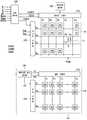
도면을 참고하면, 본 실시 예의 액정 표시장치(100)는 행 방향과 열 방향을 따라 임의의 픽셀을 가지는 액정 패널 조립체(10)와, 행 방향과 열 방향을 따라 액정 패널 조립체(10)보다 작은 수의 픽셀을 가지며 액정 패널 조립체(10) 후방에 위치하여 액정 패널 조립체(10)로 빛을 제공하는 백 라이트 유닛(40)을 포함한다.Referring to the drawings, the liquid
여기서 행 방향은 액정 표시장치(100)의 일 방향, 일례로 액정 패널 조립체(10)가 구현하는 화면의 수평 방향(일례로 도면의 x축 방향)으로 정의할 수 있고, 열 방향은 액정 표시장치(100)의 다른 일 방향, 일례로 액정 패널 조립체(10)가 구현하는 화면의 수직 방향(일례로 도면의 y축 방향)으로 정의할 수 있다.Here, the row direction may be defined as one direction of the
행 방향에 따른 액정 패널 조립체(10)의 픽셀 수와 백 라이트 유닛(40)의 픽셀 수를 각각 M과 M'라 하고, 열 방향에 따른 액정 패널 조립체(10)의 픽셀 수와 백 라이트 유닛(40)의 픽셀 수를 각각 N과 N'라 하면, 액정 패널 조립체(10)의 해상도는 M x N으로 표현할 수 있고, 백 라이트 유닛(40)의 해상도는 M' x N'로 표현할 수 있다.The number of pixels of the liquid
본 실시 예에서 액정 패널 조립체(10)의 픽셀 수를 나타내는 M과 N은 각각 240 이상의 정수로 정의할 수 있으며, 백 라이트 유닛(40)의 픽셀 수를 나타내는 M'와 N'는 각각 2 내지 99중 어느 하나의 정수로 정의할 수 있다. 백 라이트 유 닛(40)은 이러한 M' x N'의 해상도를 가지는 자발광 표시 패널로 이루어진다.In the present exemplary embodiment, M and N representing the number of pixels of the liquid
이로써 백 라이트 유닛(40)의 한 픽셀이 2개 이상의 액정 패널 조립체(10) 픽셀들에 대응하여 위치한다. 그리고 백 라이트 유닛(40)의 픽셀들은 매트릭스 형태로 배열된 구동 전극들, 일례로 서로 직교하는 방향을 따라 위치하는 주사 전극들과 데이터 전극들에 의해 온/오프와 발광 세기가 개별적으로 제어된다.Thus, one pixel of the
본 실시 예에서 백 라이트 유닛(40)의 한 픽셀은 전계 방출 어레이(Field Emission Array; FEA, 이하 'FEA'이라 한다)형 전자 방출 소자로 이루어진다.In the present embodiment, one pixel of the
FEA형 전자 방출 소자는 주사 전극과 데이터 전극, 주사 전극과 데이터 전극 중 어느 한 전극에 전기적으로 연결되는 전자 방출부 및 형광층 등을 포함한다. 전자 방출부는 일 함수(work function)가 낮거나 종횡비가 큰 물질, 일례로 탄소계 물질 또는 나노미터(nm) 사이즈 물질로 이루어질 수 있다.The FEA type electron emission device includes a scan electrode and a data electrode, an electron emission part and a fluorescent layer electrically connected to any one of the scan electrode and the data electrode. The electron emission part may be made of a material having a low work function or a high aspect ratio, for example, a carbon-based material or a nanometer (nm) size material.
FEA형 전자 방출 소자는 주사 전극과 데이터 전극의 전압 차를 이용해 전자 방출부 주위에 전계를 형성하여 이로부터 전자들을 방출시키고, 방출된 전자들로 형광층을 여기 시켜 전자빔 방출량에 상응하는 세기의 가시광을 방출시킨다.The FEA type electron emitting device forms an electric field around the electron emitting part by using the voltage difference between the scan electrode and the data electrode to emit electrons therefrom, and excites the fluorescent layer with the emitted electrons to display visible light having an intensity corresponding to the electron beam emission amount. Releases.
도 2는 도 1에 도시한 액정 패널 조립체의 부분 절개 사시도 이다.FIG. 2 is a partially cutaway perspective view of the liquid crystal panel assembly shown in FIG. 1.
도면을 참고하면, 액정 패널 조립체(10)는 서로 대향 배치되는 투명한 제1 기판(12) 및 제2 기판(14)과, 제1 기판(12)과 제2 기판(14) 사이에 주입되는 액정층(16)과, 제1 기판(12)의 내면에 위치하는 공통 전극(18)과, 제2 기판(14)의 내면에 위치하는 화소 전극들(20) 및 스위칭 소자들(22)을 포함한다. 제1 기판(12)과 제2 기판(14)의 가장자리에는 밀봉 부재(도시하지 않음)가 위치한다.Referring to the drawings, the liquid
제1 기판(12)은 액정 패널 조립체(10)의 전면 기판이 되고, 제2 기판(14)은 액정 패널 조립체(10)의 후면 기판이 된다. 제1 기판(12)과 제2 기판(14)의 외면에는 편광축이 서로 직교하는 한 쌍의 편광판(24,26)이 위치한다. 그리고 공통 전극(18)이 위치하는 제1 기판(12)의 내면과 화소 전극들(20) 및 스위칭 소자들(22)이 위치하는 제2 기판(14)의 내면은 배향막(28)으로 덮인다.The
제2 기판(14)의 내면에는 게이트 신호("주사 신호"라고도 한다)를 전달하는 복수의 게이트 라인(30)과, 데이터 신호를 전달하는 복수의 데이터 라인(32)이 형성된다. 게이트 라인들(30)은 행 방향을 따라 서로 나란하게 위치하고, 데이터 라인들(32)은 열 방향을 따라 서로 나란하게 위치한다.On the inner surface of the
화소 전극들(20)은 서브-픽셀마다 하나씩 위치하며, 각 서브-픽셀에는 게이트 라인(30) 및 데이터 라인(32)에 연결되는 스위칭 소자(22)와, 스위칭 소자(22)에 연결되는 액정 축전기(Clc, 도시하지 않음) 및 유지 축전기(Cst, 도시하지 않음)가 형성된다. 유지 축전기(Cst)는 필요에 따라 생략할 수 있다.One
스위칭 소자(22)는 박막 트랜지스터로 이루어질 수 있으며, 그 제어 단자 및 입력 단자가 각각 게이트 라인(30)과 데이터 라인(32)에 연결되고, 출력 단자는 액정 축전기(Clc)에 연결된다.The switching
그리고 제1 기판(12)과 공통 전극(18) 사이에는 칼라 필터(34)가 배치된다. 칼라 필터(34)는 하나의 서브-픽셀에 대응하는 적색과 녹색 및 청색 필터들로 구성되며, 적색과 녹색 및 청색의 3가지 필터들이 위치하는 3개의 서브-픽셀이 하나의 픽셀을 구성한다.The
전술한 구성의 액정 패널 조립체(10)에서 스위칭 소자(22)인 박막 트랜지스터가 턴 온되면, 화소 전극(20)과 공통 전극(18) 사이에 전계가 형성된다. 이 전계에 의해 액정층(16)에 위치하는 액정 분자들의 비틀림각이 변화하여 서브-픽셀별로 광 투과량을 제어함에 따라 소정의 칼라 영상을 구현한다.When the thin film transistor, which is the switching
도 3과 도 4를 참고하여 백 라이트 유닛의 제1 실시 예에 대해 설명하고, 도 5를 참고하여 백 라이트 유닛의 제2 실시 예에 대해 설명한다. 제1 및 제2 실시 예 모두 백 라이트 유닛은 FEA형 전자 방출 소자들을 포함하는 FEA형 전자 방출 표시 패널로 이루어진다.A first embodiment of the backlight unit will be described with reference to FIGS. 3 and 4, and a second embodiment of the backlight unit will be described with reference to FIG. 5. In the first and second embodiments, the backlight unit is formed of an FEA type electron emission display panel including FEA type electron emission elements.
도 3은 제1 실시 예에 따른 백 라이트 유닛의 부분 절개 사시도이고, 도 4는 도 3에 도시한 제4 기판과 전자 방출 유닛의 부분 단면도이다.3 is a partial cutaway perspective view of the backlight unit according to the first embodiment, and FIG. 4 is a partial cross-sectional view of the fourth substrate and the electron emission unit illustrated in FIG. 3.
도면을 참고하면, 백 라이트 유닛(40)은 소정의 간격을 두고 대향 배치되는 제3 기판(42)과 제4 기판(44)을 포함한다. 제3 기판(42)과 제4 기판(44)의 가장자리에는 밀봉 부재(46)가 배치되어 두 기판을 접합시키며, 내부 공간이 대략 10-6 Torr의 진공도로 배기되어 제3 기판(42)과 제4 기판(44) 및 밀봉 부재(46)가 진공 용기를 구성한다.Referring to the drawings, the
제3 기판(42)이 액정 패널 조립체를 향한 백 라이트 유닛(40)의 전면 기판이 되고, 제4 기판(44)이 백 라이트 유닛(40)의 후면 기판이 된다. 제3 기판(42)을 향한 제4 기판(44)의 일면에는 전자 방출을 위한 전자 방출 유닛(48)이 제공되고, 제4 기판(44)을 향한 제3 기판(42)의 일면에는 발광 유닛(50)이 제공된다.The
먼저 전자 방출 유닛(48)에 대해 설명하면, 전자 방출 유닛(48)은 제4 기 판(44)의 일 방향을 따라 스트라이프 패턴으로 형성되는 캐소드 전극들(52)과, 절연층(54)을 사이에 두고 캐소드 전극(52)과 직교하는 방향을 따라 스트라이프 패턴으로 형성되는 게이트 전극들(56)과, 캐소드 전극(52)에 전기적으로 연결되는 전자 방출부들(58)을 포함한다.First, the
게이트 전극들(56)은 제4 기판(44)의 행 방향을 따라 나란히 배치될 수 있고, 주사 구동 전압을 인가받아 주사 전극으로 기능할 수 있다. 캐소드 전극들(52)은 제4 기판(44)의 열 방향을 따라 나란히 배치될 수 있고, 데이터 구동 전압을 인가받아 데이터 전극으로 기능할 수 있다.The
캐소드 전극(52)과 게이트 전극(56)의 교차 영역마다 캐소드 전극(52)에 전자 방출부들(58)이 형성된다. 그리고 절연층(54)과 게이트 전극들(56)에는 각 전자 방출부(58)에 대응하는 개구부(541,561)가 형성되어 제4 기판(44) 상에 전자 방출부(58)가 노출되도록 한다. 본 실시 예에서 캐소드 전극(52)과 게이트 전극(56)의 교차 영역이 백 라이트 유닛(40)의 한 픽셀 영역에 대응한다.
전자 방출부(58)는 진공 중에서 전계가 가해지면 전자를 방출하는 물질들, 가령 탄소계 물질 또는 나노미터(nm) 사이즈 물질로 이루어진다. 전자 방출부(58)는 일례로 탄소 나노튜브, 흑연, 흑연 나노파이버, 다이아몬드, 다이아몬드상 탄소, C60, 실리콘 나노와이어 또는 이들의 조합 물질을 포함할 수 있으며, 그 제조법으로는 스크린 인쇄, 직접 성장, 화학기상증착 또는 스퍼터링 등을 포함할 수 있다.The
다른 한편으로, 전자 방출부는 몰리브덴(Mo) 또는 실리콘(Si) 등을 주 재질 로 하는 선단이 뾰족한 팁 구조물로 이루어질 수 있다.On the other hand, the electron emission portion may be formed of a tip structure having a pointed tip mainly made of molybdenum (Mo) or silicon (Si).
다음으로 제3 기판(42)에 제공되는 발광 유닛(50)은 형광층(60)과, 형광층(60)의 일면에 위치하는 애노드 전극(62)을 포함한다. 형광층(60)은 백색 형광층으로 이루어지거나, 적색과 녹색 및 청색 형광층들이 조합된 구조로 이루어질 수 있다. 도면에서는 첫 번째 경우를 도시하였다.Next, the
백색 형광층은 제3 기판(42) 전체에 형성되거나, 픽셀 영역마다 하나의 백색 형광층이 위치하도록 소정의 패턴으로 구분되어 위치할 수 있다. 적색과 녹색 및 청색 형광층들은 하나의 픽셀 영역 안에서 소정의 패턴으로 구분되어 위치할 수 있다.The white fluorescent layer may be formed on the entirety of the
애노드 전극(62)은 형광층(60) 표면을 덮는 알루미늄(Al)과 같은 금속막으로 이루어질 수 있다. 애노드 전극(62)은 전자빔을 끌어당기는 가속 전극으로서 고전압(대략 수천 볼트의 양의 직류 전압)을 인가받아 형광층(60)을 고전위 상태로 유지시키며, 형광층(60)에서 방사된 가시광 중 제4 기판(44)을 향해 방사된 가시광을 제3 기판(42) 측으로 반사시켜 화면의 휘도를 높이는 역할을 한다.The
전술한 구성에서 FEA형 전자 방출 소자는 하나의 픽셀을 구성하는 캐소드 전극(52)과 게이트 전극(56), 전자 방출부들(58) 및 이에 대응하는 형광층(60)으로 이루어진다.In the above-described configuration, the FEA type electron emission device includes a
전술한 구성에서 캐소드 전극들(52)과 게이트 전극들(56)에 소정의 구동 전압을 인가하면, 두 전극의 전압 차가 임계치 이상인 픽셀 영역에서 전자 방출부(58) 주위에 전계가 형성되어 이로부터 전자들이 방출된다. 방출된 전자들은 애 노드 전극(62)에 인가된 고전압에 이끌려 대응하는 형광층(60) 부위에 충돌함으로써 이를 발광시킨다. 픽셀별 형광층(60)의 발광 세기는 해당 픽셀의 전자빔 방출량에 상응한다.In the above configuration, when a predetermined driving voltage is applied to the
도 5는 본 발명의 제2 실시 예에 따른 백 라이트 유닛 중 전자 방출 유닛(48')의 부분 평면도이다.5 is a partial plan view of an
도면을 참고하면, 본 실시 예에서는 캐소드 전극(52')과 게이트 전극(56')의 교차 영역이 2개 이상 조합되어 하나의 픽셀 영역(A)을 구성한다. 이때 2개 이상의 캐소드 전극들(52')과, 2개 이상의 게이트 전극들(56')이 조합되어 하나의 픽셀 영역(A)을 구성하는 경우, 이 2개 이상의 캐소드 전극들(52')이 서로 전기적으로 연결되어 동일한 구동 전압을 인가받고, 2개 이상의 게이트 전극들(56') 또한 서로 전기적으로 연결되어 동일한 구동 전압을 인가받는다.Referring to the drawings, in the present embodiment, two or more intersection regions of the cathode electrode 52 'and the gate electrode 56' are combined to form one pixel region A. Referring to FIG. In this case, when two or more cathode electrodes 52 'and two or more gate electrodes 56' are combined to form one pixel region A, the two or more cathode electrodes 52 'are formed. Electrically connected to each other to receive the same driving voltage, two or more gate electrodes 56 'are also electrically connected to each other to receive the same driving voltage.
이를 위해 상기 2개 이상의 캐소드 전극들(52')과 2개 이상의 게이트 전극들(56')은 제4 기판의 가장자리로 연장되어 연성인쇄회로기판(Flexible Printed Circuit Board; FPCB) 등의 접속 부재(도시하지 않음)에 실장되는 단부가 서로 연결될 수 있다.To this end, the two or
도면에서는 일례로 3개의 캐소드 전극(52')과 3개의 게이트 전극(56')이 교차하는 9개의 교차 영역이 하나의 픽셀 영역(A)을 구성하는 경우를 도시하였다.In the drawing, as an example, nine crossing regions where three cathode electrodes 52 'and three gate electrodes 56' intersect form one pixel region A is illustrated.
전술한 제1 실시 예의 백 라이트 유닛과 제2 실시 예의 백 라이트 유닛 모두에 있어서 제3 기판(42)과 제4 기판(44) 사이에는 진공 용기에 가해지는 압축력을 지지함과 아울러 두 기판의 간격을 일정하게 유지시키는 스페이서들(64, 도 4 참 고)이 배치된다. 스페이서들(64)은 픽셀 영역의 중앙이 아닌 픽셀 영역의 외곽에 위치하는 것이 바람직하다.In both the backlight unit of the first embodiment and the backlight unit of the second embodiment, the compression force applied to the vacuum container is supported between the
또한, 필요에 따라 전면 기판인 제3 기판(42) 자체가 광 확산 기능을 구비하여 확산판으로 기능할 수 있고, 본 발명의 제3 실시 예에 따라 도 6에 도시한 바와 같이 액정 패널 조립체를 향한 제3 기판(42)의 외면에 광 확산 기능을 가지는 확산판(66)이 위치할 수 있다.In addition, if necessary, the
이와 같이 본 실시 예의 액정 표시장치(100)는 액정 패널 조립체(10)보다 작은 수의 픽셀을 가지는 일종의 저해상도 표시 패널을 백 라이트 유닛(40)으로 사용한다. 이러한 백 라이트 유닛(40)은 주사 전극들과 데이터 전극들을 이용한 패시브 매트릭스(passive matrix) 방식을 통해 구동하며, 픽셀별로 이에 대응하는 액정 패널 조립체(10) 픽셀들에 서로 다른 세기의 광을 제공한다.As described above, the
하기 표는 임의의 해상도를 가지는 액정 패널 조립체(10)에 대해 백 라이트 유닛(40)의 픽셀 수를 변경하면서 표시 품질과 구동 회로부의 제작 비용 및 제조의 용이성 등을 테스트하고, 그 결과에 따라 도출된 액정 패널 조립체(10)의 해상도별 백 라이트 유닛(40)의 최적 픽셀 수를 나타낸다.The following table tests the display quality, the manufacturing cost of the driving circuit portion, the ease of manufacture, etc. while changing the number of pixels of the

전술한 결과에 근거하여 (액정 패널 조립체 픽셀 수)/(백 라이트 유닛 픽셀 수)는 240 내지 5,852 범위가 바람직함을 알 수 있다. 상기 수치가 5,852를 초과하면 백 라이트 유닛에 의한 동적 대비비 향상 효과가 미비해지고, 상기 수치가 240 미만이면 백 라이트 유닛 제작과 구동이 어려워져 제조 비용이 상승하게 된다.Based on the above results, it can be seen that (liquid crystal panel assembly pixel number) / (backlight unit pixel number) is preferably in the range of 240 to 5,852. If the value exceeds 5,852, the effect of improving the dynamic contrast ratio by the backlight unit is insufficient, and if the value is less than 240, the manufacturing and driving of the backlight unit becomes difficult, thereby increasing the manufacturing cost.
또한, 본 실시 예에서 백 라이트 유닛(40)의 한 픽셀은 행 방향 및/또는 열 방향을 따라 2 내지 50mm의 크기로 형성될 수 있다. 행 방향 및/또는 열 방향에 따른 픽셀 크기가 2mm 미만이면 백 라이트 유닛(40)이 상당한 수의 픽셀을 갖게 되어 회로적인 신호 처리에 어려움이 있으며, 행 방향 및/또는 열 방향에 따른 픽셀 크기가 50mm를 초과하면 반대로 백 라이트 유닛(40)이 너무 작은 수의 픽셀을 갖게 되어 백 라이트 유닛(40)에 의한 화질 개선 효과가 미비해진다.In addition, in the present embodiment, one pixel of the
이와 같이 본 실시 예의 액정 표시장치(100)는 전술한 구성의 백 라이트 유닛(40)을 사용함에 따라, 종래의 냉음극 형광램프(이하 'CCFL'이라 한다) 방식 및 발광 다이오드(이하 'LED'라 한다) 방식의 백 라이트 유닛과 비교할 때 하기의 장점을 가진다.As described above, the liquid
본 실시 예의 백 라이트 유닛(40)은 면 광원이므로 CCFL 방식의 백 라이트 유닛과 LED 방식의 백 라이트 유닛에 사용되는 다수의 광학 부재를 필요로 하지 않는다. 따라서 본 실시 예의 백 라이트 유닛(40)에서는 광학 부재를 거치면서 발생하는 광 손실이 거의 없으며, 광 손실을 고려하여 백 라이트 유닛(40)에서 과도한 세기의 광을 방출하지 않아도 되므로 낮은 소비 전력으로 우수한 효율을 얻을 수 있다.Since the
또한 본 실시 예의 백 라이트 유닛(40)은 기본적으로 CCFL 방식의 백 라이트 유닛보다 소비 전력이 낮고, 광학 부재를 사용하지 않음에 따라 이에 따른 비용을 절감할 수 있으며, LED 방식의 백 라이트 유닛보다 제조 비용이 낮다. 뿐만 아니라 본 실시 예의 백 라이트 유닛(40)은 대형화가 용이하므로 30인치 이상의 대형 액정 표시장치에 용이하게 적용될 수 있다.In addition, the
도 7은 본 발명의 제3 실시 예에 따른 표시 장치를 나타낸 블록도 이다. 본 발명의 제3 실시 예에 따른 표시 장치는 수광 소자이며, 액정 소자를 사용하는 액정 패널 조립체를 포함한다. 그러나 본 발명이 이에 한정되는 것은 아니다.7 is a block diagram illustrating a display device according to a third exemplary embodiment of the present invention. The display device according to the third exemplary embodiment of the present invention is a light receiving element and includes a liquid crystal panel assembly using the liquid crystal element. However, the present invention is not limited thereto.
도 7에 도시된 바와 같이, 본 발명의 제3 실시 예에 따른 표시 장치는 액정 패널 조립체(10)와, 액정 패널 조립체(10)에 연결된 게이트 구동부(102) 및 데이터 구동부(104)와, 데이터 구동부(104)에 연결된 계조 전압 생성부(106)와, 백 라이트 유닛(40') 및 이들을 제어하는 신호 제어부(108)를 포함한다.As shown in FIG. 7, the display device according to the third exemplary embodiment of the present invention includes a liquid
액정 패널 조립체(10)는 등가 회로로 볼 때 복수의 신호선(G1-Gn, D1-Dm)과, 이 신호선에 연결되어 있으며 대략 행렬의 형태로 배열된 복수의 화소(pixel)(PX)를 포함한다. 신호선(G1-Gn, D1-Dm)은 게이트 신호("주사 신호"라고도 한다)를 전달하는 복수의 게이트 라인(G1-Gn)과, 데이터 신호를 전달하는 복수의 데이터 라인(D1-Dm)을 포함한다.The liquid
각 화소(PX), 예를 들면 i번째(i=1,2,...n) 게이트 라인(Gi)과 j번째(j=1,2,...m) 데이터 라인(Dj)에 연결된 화소(11)는 신호선(Gi,Dj)에 연결된 스위칭 소자(Q)와 이에 연결된 액정 축전기(Clc) 및 유지 축전기(Cst)를 포함한다. 유지 축전기(Cst)는 필요에 따라 생략할 수 있다.Connected to each pixel PX, for example, the i-th (i = 1,2, ... n) gate line Gi and the j-th (j = 1,2, ... m) data line Dj The
스위칭 소자(Q)는 하부 기판(도시하지 않음)에 구비되는 박막 트랜지스터 등의 삼단자 소자로서, 그 제어 단자는 게이트 라인(Gi)에 연결되어 있고, 입력 단자는 데이터 라인(Dj)에 연결되어 있으며, 출력 단자는 액정 축전기(Clc) 및 유지 축전기(Cst)와 연결되어 있다.The switching element Q is a three-terminal element such as a thin film transistor provided on a lower substrate (not shown), the control terminal of which is connected to the gate line Gi, and the input terminal of which is connected to the data line Dj. The output terminal is connected to the liquid crystal capacitor Clc and the storage capacitor Cst.
계조 전압 생성부(106)는 화소(PX)의 투과율과 관련된 두 벌의 계조 전압 집합(또는 기준 계조 전압 집합)을 생성한다. 두 벌 중 한 벌은 공통 전압(Vcom)에 대하여 양의 값을 가지며, 다른 한 벌은 음의 값을 가진다.The
게이트 구동부(102)는 액정 패널 조립체(10)의 게이트 라인(G1-Gn)과 연결되어 게이트 온 전압(Von)과 게이트 오프 전압(Voff)의 조합으로 이루어진 게이트 신호를 게이트 라인(G1-Gn)에 인가한다.The
데이터 구동부(104)는 액정 패널 조립체(10)의 데이터 라인(D1-Dm)에 연결되어 있으며, 계조 전압 생성부(106)로부터 계조 전압을 선택하고 이를 데이터 신호로서 데이터 라인(D1-Dm)에 인가한다. 그러나 계조 전압 생성부(106)가 모든 계조에 대한 전압을 모두 제공하는 것이 아니라 정해진 수의 기준 계조 전압만을 제공하는 경우에, 데이터 구동부(104)는 기준 계조 전압을 분압하여 전체 계조에 대한 계조 전압을 생성하고 이 중에서 데이터 신호를 선택한다.The
신호 제어부(108)는 게이트 구동부(102), 데이터 구동부(104) 및 백 라이트 유닛 제어부(110) 등을 제어한다. 신호 제어부(108)는 외부의 그래픽 제어기(도시하지 않음)로부터 입력 영상 신호(R, G, B) 및 이의 표시를 제어하는 입력 제어 신호를 수신한다.The
입력 영상 신호(R, G, B)는 각 화소(PX)의 휘도(luminance) 정보를 담고 있으며, 휘도는 정해진 수효, 예를 들면 1024(=210), 256(=28) 또는 64(=26)개의 계조(gray scale)를 가지고 있다. 입력 제어 신호의 예로는 수직 동기 신호(Vsync)와 수평 동기 신호(Hsync), 메인 클록(MCLK), 데이터 인에이블 신호(DE) 등이 있다.The input image signals R, G, and B contain luminance information of each pixel PX, and luminance has a predetermined number, for example, 1024 (= 210 ), 256 (= 28 ), or 64 ( = 26 ) Gray scale. Examples of the input control signal include a vertical sync signal Vsync, a horizontal sync signal Hsync, a main clock MCLK, and a data enable signal DE.
신호 제어부(108)는 입력 영상 신호(R, G, B)와 입력 제어 신호를 기초로 입력 영상 신호(R, G, B)를 액정 패널 조립체(10)의 동작 조건에 맞게 적절히 처리하고 게이트 제어 신호(CONT1) 및 데이터 제어 신호(CONT2) 등을 생성한 후, 게이트 제어 신호(CONT1)를 게이트 구동부(102)로 내보내고, 데이터 제어 신호(CONT2)와 처리한 영상 신호(DATA)를 데이터 구동부(104)에 전달한다. 또한, 신호 제어부(108)는 게이트 제어 신호(CONT1), 데이터 제어 신호(CONT2) 및 처리한 영상 신호(DATA)를 백 라이트 유닛 제어부(110)로 전달한다.The
백 라이트 유닛(40')은 백 라이트 유닛 제어부(110), 컬럼 구동부(112), 주사 구동부(114) 및 표시부(116)를 포함한다.The
주사 구동부(114)는 복수의 주사 라인(S1-Sp)에 연결되어 있으며, 주사 구동 제어 신호(CS)에 따라 각 백 라이트 유닛 화소(EPX)가 자신과 대응되는 복수의 액정 화소(EX)와 동기 되어 발광할 수 있도록, 게이트 전극에 주사 신호를 전달한다.The
컬럼 구동부(112)는 복수의 컬럼 라인(C1-Cq)에 연결되어 있으며, 발광 제어 신호(CC) 및 발광 신호(CLS)에 따라, 각 백 라이트 유닛 화소(EPX)가 자신과 대응되는 복수의 액정 화소(EX)의 계조에 대응하여 발광할 수 있도록 제어한다. 발광 신호(CLS)에 따라 복수의 발광 데이터 신호를 생성하고, 발광 제어 신호(CC)에 따라 복수의 컬럼 라인(C1-Cq)에 전달한다. 즉, 한 백 라이트 유닛 화소(EPX)에 대응하는 복수의 액정 화소(EX)에 영상이 표시되는 것에 맞추어 발광 화소(EPX)가 소정의 계조로 발광할 수 있도록 동기 시킨다.The
표시부(116)는 주사 신호를 전달하는 복수의 주사 라인(S1-Sp)과, 컬럼 신호를 전달하는 복수의 컬럼 라인(C1-Cq) 및 복수의 발광 픽셀(EPX)을 포함한다. 복수의 발광 픽셀(EPX) 각각은 주사 라인(S1-Sp)과 주사 라인에 교차하는 컬럼 라인(C1-Cq)에 의해 정의되는 영역에 위치한다. 주사 라인(S1-Sp)은 주사 구동부(114)에 연결되고, 컬럼 라인(C1-Cq)은 컬럼 구동부(112)에 연결된다. 그리고 주사 구동부(114)와 컬럼 구동부(112)는 백 라이트 유닛 제어부(110)에 연결되어 백 라이트 유닛 제어부(110)의 제어 신호에 따라 동작한다.The
상기에서 복수의 주사 라인(S1-Sp)은 전술한 백 라이트 유닛(40')의 주사 전극들이고, 컬럼 라인(C1-Cq)은 데이터 전극들이며, 각각의 발광 픽셀(EPX)은 FEA형 전자 방출 소자로 이루어진다.The plurality of scan lines S1-Sp are the scan electrodes of the above-described backlight unit 40 ', the column lines C1-Cq are the data electrodes, and each of the light emitting pixels EPX emits FEA electrons. Consists of elements.
백 라이트 유닛 제어부(110)는 표시부(116)의 블랙 영상이 표시되는 영역에 대응하는 제1 백 라이트 유닛 화소(EPX)와 그 경계면에 위치하는 복수의 제2 백 라이트 유닛 화소(EPX)의 휘도차로 인해 표시부(116)의 블랙 영상이 번지는 현상을 방지한다. 이를 위해, 제1 백 라이트 유닛 화소(EPX)의 발광 신호(CLS)를 변형하여 전달한다. 이때, 블랙 영상이란, 표시부(116)의 영상의 색상을 지칭하는 것일 수 있으나, 이에 한정되지 않으며, 영상의 휘도가 0인 경우를 통칭한다. 그리고 블랙 영상을 표시하기 위해, 백 라이트 유닛(40')이 갖는 휘도에 대응하는 계조를 이하, 블랙 계조라 한다. 이때, 블랙 계조는 백 라이트의 전원이 오프되었을 때, 백 라이트가 갖는 계조일 수 있다. 또한, 백 라이트 유닛 제어부(110)는 컬럼 구동부(112) 및 주사 구동부(114)를 제어하기 위한 제어 신호를 생성하여 전달한다.The
이하, 도 8을 참조하여 백 라이트 유닛 제어부(110)에 대해 구체적으로 설명한다.Hereinafter, the
도 8은 본 발명의 제3 실시 예에 따른 백 라이트 유닛 제어부(110)를 나타낸 블록도 이다.8 is a block diagram illustrating a
도 8에 도시된 바와 같이, 백 라이트 유닛 제어부(110)는 계조 산출부(120) 및 구동부 제어신호 생성부(130)를 포함한다.As shown in FIG. 8, the
계조 산출부(120)는 백 라이트 유닛의 한 화소(EPX)에 대응하는 복수의 액정 화소(PX)에 대한 영상 신호(DATA)를 이용하여, 백 라이트 유닛의 한 화소(EPX)에 대응하는 복수의 화소(PX) 중 가장 높은 최고 계조를 검출하고, 검출된 최고 계조에 대응하는 복수의 백 라이트 유닛 화소(EPX)의 계조를 결정한다.The
구동부 제어 신호 생성부(130)는 계조 산출부(120)로부터 복수의 백 라이트 유닛 화소(EPX)의 계조를 전달받는다. 그러면, 구동부 제어 신호 생성부(130)는 복수의 백 라이트 유닛 화소(EPX)의 계조 중 블랙 계조를 갖는 제1 백 라이트 유닛 화소(EPX)를 검출한다. 그리고, 구동부 제어 신호 생성부(130)는 제1 백 라이트 유닛 화소(EPX)의 경계면에 위치하는 복수의 제2 백 라이트 유닛 화소(EPX)의 계조를 검출한다. 그러면, 구동부 제어 신호 생성부(130)는 제1 백 라이트 유닛 화소(EPX)의 계조와 복수의 제2 백 라이트 유닛 화소(EPX)의 계조에 따른 휘도차를 임계 휘도치와 비교한다. 본 발명의 실시 예에 따른 임계 휘도치는 블랙 영상이 주위 영상에 의해 번지는 현상이 사용자에게 인식되는 것을 방지하기 위한 값으로, 사용자의 설정에 따라 다른 값을 갖을 수 있다.The driver
제1 백 라이트 유닛 화소(EPX)의 계조와 복수의 제2 백 라이트 유닛 화소(EPX)의 계조에 따른 휘도차가 임계 휘도치 보다 크지 않으면, 구동부 제어 신호 생성부(130)는 복수의 백 라이트 유닛 화소(EPX)의 계조를 디지털 데이터로 변환한다. 여기서 디지털 데이터는 발광 신호(CLS)에 포함되며 컬럼 구동부(112)로 전달된다.If the luminance difference according to the gradation of the first backlight unit pixel EPX and the gradation of the plurality of second backlight unit pixels EPX is not greater than the threshold luminance value, the driver
제1 백 라이트 유닛 화소(EPX)의 계조와 복수의 제2 백 라이트 유닛 화소(EPX)의 계조에 따른 휘도차가 임계 휘도치 보다 크면, 구동부 제어 신호 생성부(130)는 제1 백 라이트 유닛 화소(EPX)의 휘도가 점진적으로 감소 될 수 있도록하기 위해, 제1 백 라이트 유닛 화소(EPX)에 블랙 계조에 대응하는 발광 데이터 신호가 점진적으로 인가될 수 있도록 발광 제어 기간을 설정한다. 본 발명의 실시 예에 따른 발광 제어 기간은 제1 백 라이트 유닛 화소(EPX)와 복수의 제2 백 라이트 유닛 화소(EPX)의 휘도차로 인해 제1 백 라이트 유닛 화소(EPX)에 대응하는 표시부(116)의 블랙 영상이 번지는 현상을 방지하기 위해 임의로 설정되며, 발광 제어 기간은 사용자에 따라 다르게 설정될 수 있다. 구체적으로, 구동부 제어 신호 생성부(130)는 블랙 계조에 대응하는 발광 데이터 신호가 인가되는 제1 기간을 적어도 두개의 발광 제어 기간으로 구분하며, 각각의 발광 제어 기간에 인가될 계조를 결정한다. 본 발명의 실시 예에 따라 각각의 발광 제어 기간 동안에 인가되는 계조는 점차 블랙 계조에 가까워지며, 발광 제어의 마지막 기간에는 블랙 계조가 인가된다. 이때, 각각의 발광 제어 기간의 계조에 대응하는 발광 데이터 신호는 순차적으로 제1 백 라이트 유닛 화소(EPX)에 전달된다. 따라서, 구동부 제어 신호 생성부(130)는 제1 백 라이트 유닛 화소(EPX)가 점차 블랙 계조에 대응하는 휘도록 발광할 수 있도록, 각각의 발광 제어 기간에 인가되는 계조를 디지털 데이터로 변환한다. 또한, 구동부 제어 신호 생성부(130)는 제2 백 라이트 유닛 화소(EPX)가 포함된 복수의 백 라이트 유닛 화소(EPX)의 계조를 디지털 데이터로 변환한다. 이때, 제1 백 라이트 유닛 화소(EPX)에 순차적으로 인가되는 각각의 발광 제어 기간의 계조에 대한 디지털 데이터 및 나머지 복수의 백 라이트 유닛 화소(EPX)의 계조에 대한 디지털 데이터는 모두 발광 신호(CLS)에 포함되며, 컬럼 구동부(112)로 전달된다. 본 발명의 제3 실시 예에 따른 복수의 백 라이트 유닛 화소(EPX)의 발광 신호(CLS)는 8비트의 디지털 데이터를 포함 할 수 있다. 이때, 발광 신호(CLS)는 8비트의 디지털 데이터 일 수 있으나, 본 발명은 이에 한정되지 않으며, 다른 값을 가질 수 있다. 또한, 구동부 제어 신호 생성부(130)는 게이트 제어 신호(CONT1)를 이용하여 주사 구동 제어 신호(CS)를 생성하여, 주사 구동부(114)로 전달한다. 그리고, 구동부 제어 신호 생성부(130)는 데이터 제어 신호(CONT2)를 이용하여 발광 제어 신호(CC)를 생성하여, 컬럼 구동부(112)로 전달한다.If the luminance difference according to the gradation of the first backlight unit pixel EPX and the gradations of the plurality of second backlight unit pixels EPX is greater than the threshold luminance value, the driver
이하, 각 발광 제어 기간에 따라 제1 백 라이이트 유닛 화소(EPX)에 전달되는 발광 데이터 신호에 대해 구체적으로 설명한다.Hereinafter, the light emission data signal transmitted to the first backlight unit pixel EPX in each light emission control period will be described in detail.
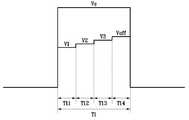
도 9는 본 발명의 제3 실시 예에 따라 제1 백 라이트 유닛 화소(EPX)에 전달되는 구동 파형을 나타내는 파형도이다.9 is a waveform diagram illustrating driving waveforms transmitted to a first backlight unit pixel EPX according to a third exemplary embodiment of the present invention.
도 9에 도시된 바와 같이, 제1 백 라이트 유닛 화소(EPX)에 발광 데이터가 신호가 인가되는 기간(T1) 동안, 주사 구동부(114)는 복수의 주사 라인(S1-Sp) 중 제1 백 라이트 유닛 화소(EPX)를 포함하는 어느 하나(Si)에 주사 온 전압(Vs)를 인가하며, 백 라이트 유닛 제어부(110)는 그에 대응하는 컬럼 라인(Cj)에 점진적으로 블랙 계조에 가까운 값을 갖는 발광 데이터 신호가 전달될 수 있도록 하기 위해, 적어도 두 개의 발광 제어 기간의 계조에 대응하는 발광 데이터 신호가 전달될 수 있도록 컬럼 구동부(112)를 제어한다.As illustrated in FIG. 9, during the period T1 during which light emission data is applied to the first backlight unit pixel EPX, the
구체적으로, 제1 발광 제어 기간(T11) 동안, 컬럼 라인(Cj)에는 블랙 계조에 대응하는 발광 데이터 신호(Voff)를 점진적으로 인가하기 위한 제1 발광 데이터 신호(V1)이 인가된다. 그러면, 제1 백 라이트 유닛 화소(EPX)는 주사 라인(Si)과 컬럼 라인(Cj)에 인가된 전압 차(Vs-V1)에 대응하는 휘도로 발광한다. 그리고, 제2 발광 제어 기간(T12) 동안, 컬럼 라인(Cj)에는 블랙 계조에 대응하는 블랙 발광 데이터 신호(Voff)를 점진적으로 인가하기 위한 제2 발광 데이터 신호(V2)가 인가된다. 그러면, 제1 백 라이트 유닛 화소(EPX)는 주사 라인(Si)과 컬럼 라인(Cj)에 인가된 전압 차(Vs-V2)에 대응하는 휘도로 발광한다. 또한, 제3 발광 제어 기간(T13) 동안, 컬럼 라인(Cj)에는 블랙 계조에 대응하는 블랙 발광 데이터 신호(Voff)를 점진적으로 인가하기 위한 제3 발광 데이터 신호(V3)가 인가된다. 그러면, 제1 백 라이트 유닛 화소(EPX)는 주사 라인(Si)과 컬럼 라인(Cj)에 인가된 전압 차(Vs-V3)에 대응하는 휘도로 발광한다. 그리고, 제4 발광 제어 기간(T14) 구간 동안, 컬럼 라인(Cj)에는 블랙 계조에 대응하는 발광 데이터 오프 신호(Voff)가 인가된다. 본 발명의 실시 예에 따른 발광 데이터 오프 신호(Voff)는 백 라이트 유닛 화소(EPX)가 발광되지 않도록 오프 시키는 오프 전압과 같은 값을 갖는다. 그러면, 제1 백 라이트 유닛 화소(EPX)는 주사 라인(Si)과 컬럼 라인(Cj)에 인가된 전압 차(Vs-Voff)가 감소하게 되어 발광하지 않는다. 따라서, 발광 제어 기간(T11-T14) 동안, 제1 백 라이트 유닛 화소(EPX)의 휘도는 점진적으로 감소하게 되어, 제1 백 라이트 유닛 화소(EPX)와 그 경계면에 위치하는 복수의 제2 백 라이트 유닛 화소(EPX)의 휘도차를 점진적으로 좁힐 수 있다. 그 결과, 점진적으로 좁혀지는 제1 백 라이트 유닛 화소(EPX)와 제2 백 라이트 유닛 화소(EPX)의 휘도차에 따라 제1 백 라이트 유닛 화소(EPX)에 대응하는 표시부(116)에 표시되는 영상이 번지는 현상을 방지 할 수 있다. 본 발명의 제3 실시 예에 따른 발광 데이터 신호를 전달하는 기간(T1)을 네 개의 발광 제어 기간(T11, T12, T13 및 T14)으로 구분하여 설명하였으나, 이에 한정되지 않으며, 기간(T1)은 적어도 두 개의 발광 제어 기간으로 구분하며, 각 발광 제어 기간은 다른 값을 갖도록 제어 할 수 있다. 즉, 도 9에 도시된 바와 같이, 각 발광 제어 기간에 인가되는 발광 데이터 신호의 전압 레벨을 상승시킴으로써, 게이트 전극(도6, 56)에 인가되는 주사 온 전압(Vs)과 캐소드 전극(도6, 52)에 인가되는 발광 데이터 신호와의 전압차를 점차 감소시켜, 제1 백 라이트 유닛 화소(EPX)의 휘도를 감소시킨다.Specifically, during the first emission control period T11, the first emission data signal V1 for gradually applying the emission data signal Voff corresponding to the black gray level is applied to the column line Cj. Then, the first backlight unit pixel EPX emits light with luminance corresponding to the voltage difference Vs-V1 applied to the scan line Si and the column line Cj. During the second emission control period T12, the second emission data signal V2 for gradually applying the black emission data signal Voff corresponding to the black gray level is applied to the column line Cj. Then, the first backlight unit pixel EPX emits light with luminance corresponding to the voltage difference Vs-V2 applied to the scan line Si and the column line Cj. In addition, during the third light emission control period T13, the third light emission data signal V3 for gradually applying the black light emission data signal Voff corresponding to the black gray level is applied to the column line Cj. Then, the first backlight unit pixel EPX emits light with luminance corresponding to the voltage difference Vs-V3 applied to the scan line Si and the column line Cj. During the fourth light emission control period T14, the light emission data off signal Voff corresponding to the black gray level is applied to the column line Cj. The light emission data off signal Voff according to an embodiment of the present invention has a value equal to an off voltage for turning off the backlight unit pixel EPX so as not to emit light. Then, the first backlight unit pixel EPX reduces the voltage difference Vs-Voff applied to the scan line Si and the column line Cj and does not emit light. Therefore, during the light emission control periods T11-T14, the luminance of the first backlight unit pixel EPX gradually decreases, so that the first backlight unit pixel EPX and the plurality of second bags positioned at the interface thereof are thus reduced. The luminance difference between the light unit pixels EPX may be gradually narrowed. As a result, the
도 10은 본 발명의 제3 실시 예에 따른 제1 백 라이트 유닛(EPX)의 휘도를 점진적으로 감소시키는 방법을 나타내는 순서도이다.FIG. 10 is a flowchart illustrating a method of gradually decreasing luminance of a first backlight unit EPX according to a third embodiment of the present invention.
먼저, 백 라이트 유닛 제어부(110)는 백 라이트 유닛의 한 화소(EPX)에 대응하는 복수의 액정 화소(PX)에 대한 영상 신호(DATA)를 이용하여, 백 라이트 유닛(40')의 한 화소(EPX)에 대응하는 복수의 화소(PX) 중 가장 높은 계조를 검출하고, 검출된 계조에 대응하는 복수의 백 라이트 유닛 화소(EPX)의 계조를 결정한다(S100).First, the
백 라이트 유닛 제어부(110)는 복수의 백 라이트 유닛 화소(EPX)의 계조 중 블랙 계조를 갖는 제1 백 라이트 유닛 화소(EPX)를 검출한다(S200).The
백 라이트 유닛 제어부(110)는 블랙 계조를 갖는 제1 백 라이트 유닛 화소(EPX)와 그 경계면에 위치하는 복수의 제2 백 라이트 유닛 화소(EPX)의 계조에 따른 휘도차와 임계 휘도치를 비교한다(S300).The
S300 단계에서 비교 결과, 제1 백 라이트 유닛 화소(EPX)의 계조와 복수의 제2 백 라이트 유닛 화소(EPX)의 계조에 따른 휘도차가 임계 휘도치 보다 크면, 백 라이트 유닛 제어부(110)는 제1 백 라이트 유닛 화소(EPX)의 휘도가 점진적으로 감소 될 수 있도록 하기 위해, 발광 데이터 신호가 전달되는 기간(T1)을 적어도 두 개의 발광 제어 기간으로 구분하며, 제1 백 라이트 유닛 화소(EPX)에 각각의 발광 제어 기간의 계조에 대응하는 발광 데이터 신호가 순차적으로 인가 될 수 있도록 컬럼 구동부(112)를 제어한다. 그러면, 제1 백 라이트 유닛 화소(EPX)는 각각의 발광 제어 기간의 계조가 인가될수록 점차 블랙 계조에 대응하는 휘도로 발광하며, 발광 제어의 마지막 기간에는 블랙 계조에 대한 휘도록 발광한다. 따라서, 제1 백 라이트 유닛 화소(EPX)의 휘도는 점진적으로 감소될 수 있다.(S400) S300 단계에서 비교 결과, 제1 백 라이트 유닛 화소(EPX)의 계조와 복수의 제2 백 라이트 유닛 화소(EPX)의 계조에 따른 휘도차가 임계 휘도치 보다 크지 않으면, 백 라이트 유닛 제어부(110)는 제1 및 제2 백 라이트 유닛 화소(EPX)를 포함하는 복수의 백 라이트 유닛 화소(EPX)의 계조에 대응하여 발광하도록 제어한다.As a result of the comparison in operation S300, when the luminance difference according to the gradation of the first backlight unit pixel EPX and the gradations of the plurality of second backlight unit pixels EPX is greater than the threshold luminance value, the
이와 같이, 제1 백 라이트 유닛 화소(EPX)의 계조와 복수의 제2 백 라이트 유닛 화소(EPX)의 계조에 따른 휘도차가 임계 휘도치 보다 크면, 제1 백 라이트 유닛 화소(EPX)의 휘도가 점진적으로 감소 될 수 있도록 하기 위해, 블랙 계조에 대응하는 발광 데이터 신호가 인가되는 제1 기간을 적어도 두 개의 발광 제어 기간으로 구분하며, 각각의 발광 제어 기간의 계조에 대응하는 발광 데이터 신호를 순차적으로 제1 백 라이트 유닛 화소(EPX)에 전달함으로써, 제1 백 라이트 유닛 화소(EPX)에 대응하는 표시부(116)에 표시 되는 영상이 번지는 현상을 가시적으로 인식하지 못하게 할 수 있다.As described above, when the luminance difference according to the gradation of the first backlight unit pixel EPX and the gradations of the plurality of second backlight unit pixels EPX is larger than the threshold luminance value, the luminance of the first backlight unit pixel EPX is increased. In order to be gradually reduced, the first period during which the emission data signal corresponding to the black gradation is applied is divided into at least two emission control periods, and the emission data signal corresponding to the gradation of each emission control period is sequentially By transmitting to the first backlight unit pixel EPX, it is possible to prevent visual recognition of a phenomenon in which an image displayed on the
지금까지 액정 패널 조립체를 사용하는 표시 장치를 이용하는 실시 예에 대해서 서술하였으나, 본 발명은 이에 한정되지 않는다. 자발광이 아닌 표시 장치로서, 백 라이트 유닛으로부터 수광하여 영상을 표시하는 표시 장치에 모두 적용가능하다.An embodiment using a display device using a liquid crystal panel assembly has been described so far, but the present invention is not limited thereto. As a display device other than self-luminous, it is applicable to both display devices that receive images from a backlight unit and display an image.
상기에서는 본 발명의 바람직한 실시 예에 대하여 설명하였지만, 본 발명은 이에 한정되는 것이 아니고 특허청구범위와 발명의 상세한 설명 및 첨부한 도면의 범위 안에서 여러 가지로 변형하여 실시하는 것이 가능하고 이 또한 본 발명의 범위에 속하는 것은 당연하다.Although the preferred embodiments of the present invention have been described above, the present invention is not limited thereto, and various modifications and changes can be made within the scope of the claims and the detailed description of the invention and the accompanying drawings. Naturally, it belongs to the range of.
본 발명의 특징에 따른 발광장치 및 이를 이용한 표시장치, 발광장치의 구동방법 및 표시 장치의 구동방법은 복수의 백 라이트 유닛 화소 중 블랙 계조를 갖는 화소의 휘도를 점차 블랙 계조에 대응하는 휘도가 되도록 제어하여 블랙 계조를 갖는 백 라이트 유닛 화소에 대응하여 표시되는 영상이 번지는 현상을 방지할 수 있 다.According to an aspect of the present invention, there is provided a light emitting device, a display device using the same, a method of driving the light emitting device, and a method of driving the display device such that the luminance of a pixel having a black gray level among the plurality of backlight unit pixels gradually becomes a luminance corresponding to the black gray level. By controlling, the blurring of the displayed image corresponding to the backlight unit pixel having the black gradation can be prevented.
Claims (10)
Translated fromKoreanPriority Applications (1)
| Application Number | Priority Date | Filing Date | Title |
|---|---|---|---|
| KR1020070030428AKR20080088066A (en) | 2007-03-28 | 2007-03-28 | Light emitting device, display device using same, driving method of light emitting device and driving method of display device |
Applications Claiming Priority (1)
| Application Number | Priority Date | Filing Date | Title |
|---|---|---|---|
| KR1020070030428AKR20080088066A (en) | 2007-03-28 | 2007-03-28 | Light emitting device, display device using same, driving method of light emitting device and driving method of display device |
Publications (1)
| Publication Number | Publication Date |
|---|---|
| KR20080088066Atrue KR20080088066A (en) | 2008-10-02 |
Family
ID=40150408
Family Applications (1)
| Application Number | Title | Priority Date | Filing Date |
|---|---|---|---|
| KR1020070030428AWithdrawnKR20080088066A (en) | 2007-03-28 | 2007-03-28 | Light emitting device, display device using same, driving method of light emitting device and driving method of display device |
Country Status (1)
| Country | Link |
|---|---|
| KR (1) | KR20080088066A (en) |
Cited By (2)
| Publication number | Priority date | Publication date | Assignee | Title |
|---|---|---|---|---|
| CN114779530A (en)* | 2022-05-16 | 2022-07-22 | 中国民用航空飞行学院 | A low halo Mini-LED backlight display |
| WO2022217730A1 (en)* | 2021-04-16 | 2022-10-20 | Tcl华星光电技术有限公司 | Grayscale control method and display panel |
- 2007
- 2007-03-28KRKR1020070030428Apatent/KR20080088066A/ennot_activeWithdrawn
Cited By (4)
| Publication number | Priority date | Publication date | Assignee | Title |
|---|---|---|---|---|
| WO2022217730A1 (en)* | 2021-04-16 | 2022-10-20 | Tcl华星光电技术有限公司 | Grayscale control method and display panel |
| US11948491B2 (en) | 2021-04-16 | 2024-04-02 | Tcl China Star Optoelectronics Technology Co., Ltd | Grayscale controlling method and display panel |
| CN114779530A (en)* | 2022-05-16 | 2022-07-22 | 中国民用航空飞行学院 | A low halo Mini-LED backlight display |
| CN114779530B (en)* | 2022-05-16 | 2023-08-15 | 中国民用航空飞行学院 | Low halation type Mini-LED backlight display |
Similar Documents
| Publication | Publication Date | Title |
|---|---|---|
| KR100869800B1 (en) | Display device and driving method thereof | |
| KR100759413B1 (en) | A light emitting device and a liquid crystal display device using the light emitting device as a backlight unit | |
| JP4758952B2 (en) | Light emitting device and display device using the same as light source | |
| JP2007310369A (en) | Display device, display device driving method, and liquid crystal display device | |
| US20090135127A1 (en) | Display device and driving method thereof | |
| KR100863961B1 (en) | Light emitting device, display device using same, driving method of light emitting device and driving method of display device | |
| KR100839411B1 (en) | Liquid crystal display | |
| KR20090068756A (en) | Light emitting device, display device using same, driving method of light emitting device | |
| JP2008124027A (en) | Light emitting device and display device | |
| KR20080088066A (en) | Light emitting device, display device using same, driving method of light emitting device and driving method of display device | |
| EP2023316B1 (en) | Light emission device, display using the light emission device, and method of driving the light emission device. | |
| US20090135212A1 (en) | Light emitting device, driving method for the light emitting device, and display device using the light emitting device | |
| KR100823492B1 (en) | Display device and driving method thereof | |
| US20090135119A1 (en) | Light emitting device and display device having the same | |
| KR20080088065A (en) | Light emitting device, display device using same, driving method of light emitting device and driving method of display device | |
| KR100749424B1 (en) | Light-emitting device and liquid crystal display device using this light-emitting device as backlight unit | |
| KR20080080867A (en) | Display device and driving method thereof | |
| KR20080075662A (en) | Light emitting device, display device using same, driving method of light emitting device and driving method of display device | |
| KR20080045895A (en) | A diffusion member, a light emitting device having the diffusion member, and a display device having the light emitting device | |
| KR100717762B1 (en) | Light-emitting device and liquid crystal display device using this light-emitting device as backlight unit | |
| KR100823189B1 (en) | Light emitting device and liquid crystal display using the same as back light unit | |
| KR20080043532A (en) | Light emitting device and display device having same | |
| KR100814841B1 (en) | Light emitting device and liquid crystal display using the same as back light unit | |
| KR100814848B1 (en) | Light-emitting device and liquid crystal display device using this light-emitting device as backlight unit | |
| KR20090126059A (en) | Light emitting device, display device including same and driving method thereof |
Legal Events
| Date | Code | Title | Description |
|---|---|---|---|
| PA0109 | Patent application | Patent event code:PA01091R01D Comment text:Patent Application Patent event date:20070328 | |
| PG1501 | Laying open of application | ||
| PC1203 | Withdrawal of no request for examination | ||
| WITN | Application deemed withdrawn, e.g. because no request for examination was filed or no examination fee was paid |