KR20080086371A - Display device, driving method thereof and electronic device - Google Patents
Display device, driving method thereof and electronic deviceDownload PDFInfo
- Publication number
- KR20080086371A KR20080086371AKR1020080025738AKR20080025738AKR20080086371AKR 20080086371 AKR20080086371 AKR 20080086371AKR 1020080025738 AKR1020080025738 AKR 1020080025738AKR 20080025738 AKR20080025738 AKR 20080025738AKR 20080086371 AKR20080086371 AKR 20080086371A
- Authority
- KR
- South Korea
- Prior art keywords
- driving transistor
- gate
- signal
- line
- transistor
- Prior art date
- Legal status (The legal status is an assumption and is not a legal conclusion. Google has not performed a legal analysis and makes no representation as to the accuracy of the status listed.)
- Ceased
Links
- 238000000034methodMethods0.000titleclaimsdescription72
- 239000011159matrix materialSubstances0.000claimsabstractdescription18
- 238000005070samplingMethods0.000claimsdescription63
- 239000003990capacitorSubstances0.000claimsdescription61
- 230000008569processEffects0.000claimsdescription61
- 238000007906compressionMethods0.000claimsdescription13
- 238000002360preparation methodMethods0.000claimsdescription12
- 238000001454recorded imageMethods0.000claims2
- 239000008186active pharmaceutical agentSubstances0.000description28
- 238000010586diagramMethods0.000description13
- 241000750042ViniSpecies0.000description8
- 230000007704transitionEffects0.000description7
- 101100191136Arabidopsis thaliana PCMP-A2 geneProteins0.000description6
- 101100422768Saccharomyces cerevisiae (strain ATCC 204508 / S288c) SUL2 geneProteins0.000description6
- 101100048260Saccharomyces cerevisiae (strain ATCC 204508 / S288c) UBX2 geneProteins0.000description6
- 239000000758substrateSubstances0.000description6
- 239000010409thin filmSubstances0.000description6
- 230000008859changeEffects0.000description5
- 101150010989VCATH geneProteins0.000description4
- 230000008878couplingEffects0.000description3
- 238000010168coupling processMethods0.000description3
- 238000005859coupling reactionMethods0.000description3
- 230000006870functionEffects0.000description3
- 238000004020luminiscence typeMethods0.000description3
- 230000004044responseEffects0.000description3
- 230000002441reversible effectEffects0.000description3
- 230000002159abnormal effectEffects0.000description2
- 239000000853adhesiveSubstances0.000description2
- 239000010408filmSubstances0.000description2
- 239000011521glassSubstances0.000description2
- 238000009499grossingMethods0.000description2
- 229910021420polycrystalline siliconInorganic materials0.000description2
- 229920005591polysiliconPolymers0.000description2
- 206010047571Visual impairmentDiseases0.000description1
- 230000002411adverseEffects0.000description1
- 230000006399behaviorEffects0.000description1
- 239000003086colorantSubstances0.000description1
- 230000006835compressionEffects0.000description1
- 238000001514detection methodMethods0.000description1
- 230000005684electric fieldEffects0.000description1
- 238000005286illuminationMethods0.000description1
- 238000003384imaging methodMethods0.000description1
- 230000001681protective effectEffects0.000description1
- 230000001052transient effectEffects0.000description1
Images


Classifications
- G—PHYSICS
- G09—EDUCATION; CRYPTOGRAPHY; DISPLAY; ADVERTISING; SEALS
- G09G—ARRANGEMENTS OR CIRCUITS FOR CONTROL OF INDICATING DEVICES USING STATIC MEANS TO PRESENT VARIABLE INFORMATION
- G09G3/00—Control arrangements or circuits, of interest only in connection with visual indicators other than cathode-ray tubes
- G09G3/20—Control arrangements or circuits, of interest only in connection with visual indicators other than cathode-ray tubes for presentation of an assembly of a number of characters, e.g. a page, by composing the assembly by combination of individual elements arranged in a matrix no fixed position being assigned to or needed to be assigned to the individual characters or partial characters
- G09G3/22—Control arrangements or circuits, of interest only in connection with visual indicators other than cathode-ray tubes for presentation of an assembly of a number of characters, e.g. a page, by composing the assembly by combination of individual elements arranged in a matrix no fixed position being assigned to or needed to be assigned to the individual characters or partial characters using controlled light sources
- G09G3/30—Control arrangements or circuits, of interest only in connection with visual indicators other than cathode-ray tubes for presentation of an assembly of a number of characters, e.g. a page, by composing the assembly by combination of individual elements arranged in a matrix no fixed position being assigned to or needed to be assigned to the individual characters or partial characters using controlled light sources using electroluminescent panels
- G09G3/32—Control arrangements or circuits, of interest only in connection with visual indicators other than cathode-ray tubes for presentation of an assembly of a number of characters, e.g. a page, by composing the assembly by combination of individual elements arranged in a matrix no fixed position being assigned to or needed to be assigned to the individual characters or partial characters using controlled light sources using electroluminescent panels semiconductive, e.g. using light-emitting diodes [LED]
- G09G3/3208—Control arrangements or circuits, of interest only in connection with visual indicators other than cathode-ray tubes for presentation of an assembly of a number of characters, e.g. a page, by composing the assembly by combination of individual elements arranged in a matrix no fixed position being assigned to or needed to be assigned to the individual characters or partial characters using controlled light sources using electroluminescent panels semiconductive, e.g. using light-emitting diodes [LED] organic, e.g. using organic light-emitting diodes [OLED]
- G09G3/3225—Control arrangements or circuits, of interest only in connection with visual indicators other than cathode-ray tubes for presentation of an assembly of a number of characters, e.g. a page, by composing the assembly by combination of individual elements arranged in a matrix no fixed position being assigned to or needed to be assigned to the individual characters or partial characters using controlled light sources using electroluminescent panels semiconductive, e.g. using light-emitting diodes [LED] organic, e.g. using organic light-emitting diodes [OLED] using an active matrix
- G09G3/3233—Control arrangements or circuits, of interest only in connection with visual indicators other than cathode-ray tubes for presentation of an assembly of a number of characters, e.g. a page, by composing the assembly by combination of individual elements arranged in a matrix no fixed position being assigned to or needed to be assigned to the individual characters or partial characters using controlled light sources using electroluminescent panels semiconductive, e.g. using light-emitting diodes [LED] organic, e.g. using organic light-emitting diodes [OLED] using an active matrix with pixel circuitry controlling the current through the light-emitting element
- G—PHYSICS
- G02—OPTICS
- G02F—OPTICAL DEVICES OR ARRANGEMENTS FOR THE CONTROL OF LIGHT BY MODIFICATION OF THE OPTICAL PROPERTIES OF THE MEDIA OF THE ELEMENTS INVOLVED THEREIN; NON-LINEAR OPTICS; FREQUENCY-CHANGING OF LIGHT; OPTICAL LOGIC ELEMENTS; OPTICAL ANALOGUE/DIGITAL CONVERTERS
- G02F1/00—Devices or arrangements for the control of the intensity, colour, phase, polarisation or direction of light arriving from an independent light source, e.g. switching, gating or modulating; Non-linear optics
- G02F1/01—Devices or arrangements for the control of the intensity, colour, phase, polarisation or direction of light arriving from an independent light source, e.g. switching, gating or modulating; Non-linear optics for the control of the intensity, phase, polarisation or colour
- G02F1/13—Devices or arrangements for the control of the intensity, colour, phase, polarisation or direction of light arriving from an independent light source, e.g. switching, gating or modulating; Non-linear optics for the control of the intensity, phase, polarisation or colour based on liquid crystals, e.g. single liquid crystal display cells
- G02F1/133—Constructional arrangements; Operation of liquid crystal cells; Circuit arrangements
- G—PHYSICS
- G09—EDUCATION; CRYPTOGRAPHY; DISPLAY; ADVERTISING; SEALS
- G09G—ARRANGEMENTS OR CIRCUITS FOR CONTROL OF INDICATING DEVICES USING STATIC MEANS TO PRESENT VARIABLE INFORMATION
- G09G3/00—Control arrangements or circuits, of interest only in connection with visual indicators other than cathode-ray tubes
- G09G3/20—Control arrangements or circuits, of interest only in connection with visual indicators other than cathode-ray tubes for presentation of an assembly of a number of characters, e.g. a page, by composing the assembly by combination of individual elements arranged in a matrix no fixed position being assigned to or needed to be assigned to the individual characters or partial characters
- G09G3/22—Control arrangements or circuits, of interest only in connection with visual indicators other than cathode-ray tubes for presentation of an assembly of a number of characters, e.g. a page, by composing the assembly by combination of individual elements arranged in a matrix no fixed position being assigned to or needed to be assigned to the individual characters or partial characters using controlled light sources
- G09G3/30—Control arrangements or circuits, of interest only in connection with visual indicators other than cathode-ray tubes for presentation of an assembly of a number of characters, e.g. a page, by composing the assembly by combination of individual elements arranged in a matrix no fixed position being assigned to or needed to be assigned to the individual characters or partial characters using controlled light sources using electroluminescent panels
- G09G3/32—Control arrangements or circuits, of interest only in connection with visual indicators other than cathode-ray tubes for presentation of an assembly of a number of characters, e.g. a page, by composing the assembly by combination of individual elements arranged in a matrix no fixed position being assigned to or needed to be assigned to the individual characters or partial characters using controlled light sources using electroluminescent panels semiconductive, e.g. using light-emitting diodes [LED]
- H—ELECTRICITY
- H05—ELECTRIC TECHNIQUES NOT OTHERWISE PROVIDED FOR
- H05B—ELECTRIC HEATING; ELECTRIC LIGHT SOURCES NOT OTHERWISE PROVIDED FOR; CIRCUIT ARRANGEMENTS FOR ELECTRIC LIGHT SOURCES, IN GENERAL
- H05B33/00—Electroluminescent light sources
- H05B33/12—Light sources with substantially two-dimensional radiating surfaces
- G—PHYSICS
- G09—EDUCATION; CRYPTOGRAPHY; DISPLAY; ADVERTISING; SEALS
- G09G—ARRANGEMENTS OR CIRCUITS FOR CONTROL OF INDICATING DEVICES USING STATIC MEANS TO PRESENT VARIABLE INFORMATION
- G09G2300/00—Aspects of the constitution of display devices
- G09G2300/08—Active matrix structure, i.e. with use of active elements, inclusive of non-linear two terminal elements, in the pixels together with light emitting or modulating elements
- G09G2300/0809—Several active elements per pixel in active matrix panels
- G09G2300/0819—Several active elements per pixel in active matrix panels used for counteracting undesired variations, e.g. feedback or autozeroing
- G—PHYSICS
- G09—EDUCATION; CRYPTOGRAPHY; DISPLAY; ADVERTISING; SEALS
- G09G—ARRANGEMENTS OR CIRCUITS FOR CONTROL OF INDICATING DEVICES USING STATIC MEANS TO PRESENT VARIABLE INFORMATION
- G09G2300/00—Aspects of the constitution of display devices
- G09G2300/08—Active matrix structure, i.e. with use of active elements, inclusive of non-linear two terminal elements, in the pixels together with light emitting or modulating elements
- G09G2300/0809—Several active elements per pixel in active matrix panels
- G09G2300/0842—Several active elements per pixel in active matrix panels forming a memory circuit, e.g. a dynamic memory with one capacitor
- G—PHYSICS
- G09—EDUCATION; CRYPTOGRAPHY; DISPLAY; ADVERTISING; SEALS
- G09G—ARRANGEMENTS OR CIRCUITS FOR CONTROL OF INDICATING DEVICES USING STATIC MEANS TO PRESENT VARIABLE INFORMATION
- G09G2310/00—Command of the display device
- G09G2310/02—Addressing, scanning or driving the display screen or processing steps related thereto
- G09G2310/0243—Details of the generation of driving signals
- G09G2310/0254—Control of polarity reversal in general, other than for liquid crystal displays
- G09G2310/0256—Control of polarity reversal in general, other than for liquid crystal displays with the purpose of reversing the voltage across a light emitting or modulating element within a pixel
- G—PHYSICS
- G09—EDUCATION; CRYPTOGRAPHY; DISPLAY; ADVERTISING; SEALS
- G09G—ARRANGEMENTS OR CIRCUITS FOR CONTROL OF INDICATING DEVICES USING STATIC MEANS TO PRESENT VARIABLE INFORMATION
- G09G2310/00—Command of the display device
- G09G2310/02—Addressing, scanning or driving the display screen or processing steps related thereto
- G09G2310/0264—Details of driving circuits
- G09G2310/0297—Special arrangements with multiplexing or demultiplexing of display data in the drivers for data electrodes, in a pre-processing circuitry delivering display data to said drivers or in the matrix panel, e.g. multiplexing plural data signals to one D/A converter or demultiplexing the D/A converter output to multiple columns
Landscapes
- Engineering & Computer Science (AREA)
- Physics & Mathematics (AREA)
- General Physics & Mathematics (AREA)
- Computer Hardware Design (AREA)
- Theoretical Computer Science (AREA)
- Nonlinear Science (AREA)
- Chemical & Material Sciences (AREA)
- Crystallography & Structural Chemistry (AREA)
- Mathematical Physics (AREA)
- Optics & Photonics (AREA)
- Control Of Indicators Other Than Cathode Ray Tubes (AREA)
- Control Of El Displays (AREA)
- Electroluminescent Light Sources (AREA)
Abstract
Translated fromKoreanDescription
Translated fromKorean우선권 정보Priority Information
본 발명은 2007년 3월 22일자로 일본특허청에 특허출원된 일본특허원 제2007-74985호를 우선권으로 주장한다.The present invention claims priority of Japanese Patent Application No. 2007-74985 filed with the Japan Patent Office on March 22, 2007.
기술 분야Technical field
본 발명은 발광 소자를 화소에 이용한 액티브 매트릭스형의 표시 장치 및 그 구동 방법에 관한 것이다. 또한 이와 같은 표시 장치를 이용한 전자기기에 관한 것이다.The present invention relates to an active matrix display device using a light emitting element for a pixel and a driving method thereof. It also relates to an electronic device using such a display device.
발광 소자로서 유기 EL 디바이스를 이용한 평면 자발광형의 표시 장치의 개발이 근래 왕성하게 되어 있다. 유기 EL 디바이스는 유기 박막에 전계를 걸면 발광하는 현상을 이용한 디바이스이다. 유기 EL 디바이스는 인가 전압이 10V 이하에서 구동하기 때문에 저소비 전력이다. 또한 유기 EL 디바이스는 스스로 광을 발하는 자발광 소자이기 때문에, 조명 부재를 필요로 하지 않아 경량화 및 박형화가 용이 하다. 또한 유기 EL 디바이스의 응답 속도는 수㎲ 정도로 매우 고속이기 때문에, 동화 표시시의 잔상이 발생하지 않는다.The development of a planar self-luminous display device using an organic EL device as a light emitting element has been actively developed in recent years. An organic EL device is a device using a phenomenon of emitting light when an electric field is applied to an organic thin film. The organic EL device has low power consumption because the applied voltage is driven at 10V or less. In addition, since the organic EL device is a self-luminous element that emits light by itself, it does not require an illumination member, so that the weight and thickness are easy. In addition, since the response speed of the organic EL device is very high at several orders of magnitude, no afterimage occurs during moving picture display.
유기 EL 디바이스를 화소에 이용한 평면 자발광형의 표시 장치중에서도, 특히 구동 소자로서 박막 트랜지스터를 각 화소에 집적(集積) 형성한 액티브 매트릭스형의 표시 장치의 개발이 왕성하다. 액티브 매트릭스형 평면 자발광 표시 장치는, 예를 들면 일본 특개2003-255856, 일본 특개2003-271095, 일본 특개2004-133240, 일본 특개2004-029791 및 일본 특개2004-093682(이하, 특허문헌1 내지 특허문헌5로 칭함)에 개시되어 있다.In the planar self-luminous display device using an organic EL device as a pixel, development of an active matrix type display device in which a thin film transistor is formed in each pixel as a driving element is particularly active. Examples of the active matrix flat self-emission display device include Japanese Patent Laid-Open No. 2003-255856, Japanese Patent Laid-Open No. 2003-271095, Japanese Patent Laid-Open 2004-133240, Japanese Patent Laid-Open No. 2004-029791 and Japanese Patent Laid-Open No. 2004-093682 Reference Document 5).
그러나, 종래의 액티브 매트릭스형 평면 자발광형 표시 장치에서는, 프로세스 변동에 의해 발광 소자를 구동하는 트랜지스터의 임계 전압이 변동된다는 문제점이 있다. 이와 같은 구동 트랜지스터의 특성 편차는 발광 휘도에 영향을 주어 버린다. 표시 장치의 화면 전체에 걸쳐서 발광 휘도를 균일하게 제어하기 위해, 각 화소 회로 내에서 상술한 구동 트랜지스터의 임계 전압의 편차를 보정할 필요가 있다. 종래로부터 이러한 임계 전압 보정 기능을 화소마다 구비한 표시 장치가 제안되어 있다.However, in the conventional active matrix flat self-luminous display device, there is a problem that the threshold voltage of the transistor driving the light emitting element is changed by the process variation. Such variation in characteristics of the driving transistor affects the light emission luminance. In order to uniformly control the luminescence brightness over the entire screen of the display device, it is necessary to correct the above-described deviation of the threshold voltage of the driving transistor in each pixel circuit. Conventionally, a display device having such a threshold voltage correction function for each pixel has been proposed.
종래의 화소 회로는, 임계 전압 보정 동작을 수행한 후 영상 신호를 샘플링하고, 이것에 의거하여 발광 소자를 구동한다. 그러나 임계 전압 보정 동작부터 발광 동작의 사이에서, 구동 트랜지스터에 전류 리크가 생기기 때문에, 반드시는 임계 전압 보정 동작이 정확하게 행하여지지 않고, 오차가 생기고 있다. 이 임계 전압 보정 동작의 오차 또는 편차에 의해, 발광 휘도에 얼룩이 생기고, 화상 품위를 손상시키게 된다.A conventional pixel circuit samples a video signal after performing a threshold voltage correction operation, and drives a light emitting element based on this. However, since current leakage occurs in the driving transistor between the threshold voltage correction operation and the light emission operation, the threshold voltage correction operation is not always performed correctly, and an error occurs. Due to the error or deviation of the threshold voltage correction operation, unevenness occurs in the luminescence brightness, resulting in damage to the image quality.
상술한 종래의 기술의 과제를 감안하여, 본 발명은 구동 트랜지스터의 전류 리크를 억제하여 임계 전압 보정 동작의 정밀도를 개선하고, 따라서 발광 휘도 얼룩이 없는 표시 장치를 제공하는 것을 목적으로 하다. 본 발명의 제 1의 실시 형태에 따르면, 표시 장치가 제공된다. 이 표시 장치는, 화소 어레이부와 구동부를 포 함하고, 상기 화소 어레이부는, 급전선과, 행형상의 주사선과, 열형상의 신호선과, 각 주사선과 각 신호선이 교차하는 부분에 배치된 행렬형상의 화소를 구비하고, 각 화소는, 적어도 샘플링 트랜지스터와, 구동 트랜지스터와, 발광 소자와, 커패시터를 구비한다. 상기 샘플링 트랜지스터는, 그 제어 단자가 상기 주사선에 접속되고, 상기 샘플링 트랜지스터의 한 쌍의 전류 단자 중 하나가 상기 주사선에 접속하고 상기 한 한 쌍의 전류 단자 중 나머지 하나가 상기 구동 트랜지스터의 제어 단자 사이에 접속한다. 상기 구동 트랜지스터는, 한 쌍의 전류 단자의 하나가 상기 발광 소자에 접속하고, 나머지 하나가 급전선에 접속한다. 상기 구동부는, 각 주사선에 제어 신호를 공급하고 각 신호선에 영상 신호를 공급하여 각 화소를 구동하고, 상기 구동 트랜지스터의 임계 전압의 편차를 보정하는 임계 전압 보정 동작과, 상기 영상 신호를 상기 커패시터에 기록하는 기록 동작, 및 기록된 영상 신호에 따라 상기 발광 소자를 발광시키는 발광 동작을 수행한다. 상기 임계 전압 보정 동작은: 상기 구동 트랜지스터의 게이트인 제어 단자를 기준 전위로 유지하면서, 상기 구동 트랜지스터의 소스인 전류 단자와의 사이의 게이트 소스 전압을 상기 임계 전압보다 높게 설정하여 상기 구동 트랜지스터를 온 상태로 하는 준비 과정과; 상기 게이트를 기준 전위로 유지한 채로 상기 구동 트랜지스터를 통전하여 상기 구동 트랜지스터가 컷오프한 때 상기 게이트와 소스 사이에 나타나는 상기 임계 전압에 상당하는 전압을 상기 기억 커패시터에 보존하는 통전 과정과; 상기 게이트에 인가되는 상기 기준 전위를 변경하여 상기 게이트 소스 전압을 상기 임계 전압에 상당하는 전압보다도 압축하여, 상기 구동 트랜지스터를 확실하게 오프 상태로 하는 압축 과 정을 포함한다.In view of the above-mentioned problems of the prior art, the present invention aims to provide a display device which suppresses current leakage of a driving transistor to improve the accuracy of the threshold voltage correction operation, and thus has no emission luminance unevenness. According to the first embodiment of the present invention, a display device is provided. The display device includes a pixel array portion and a driver portion, wherein the pixel array portion includes matrix pixels arranged at a portion where a feed line, a row scan line, a columnar signal line, and each scan line and each signal line cross each other. Each pixel includes at least a sampling transistor, a driving transistor, a light emitting element, and a capacitor. The sampling transistor has a control terminal connected to the scan line, one of the pair of current terminals of the sampling transistor is connected to the scan line, and the other of the pair of current terminals is connected between the control terminal of the driving transistor. Connect to In the driving transistor, one of a pair of current terminals is connected to the light emitting element, and the other is connected to a feed line. The driving unit supplies a control signal to each scan line and supplies an image signal to each signal line to drive each pixel, and performs a threshold voltage correction operation to correct a deviation of a threshold voltage of the driving transistor, and transmits the image signal to the capacitor. A recording operation for recording and a light emitting operation for emitting the light emitting element in accordance with the recorded video signal are performed. The threshold voltage correction operation may include: turning on the driving transistor by setting a gate source voltage between the current terminal, which is a source of the driving transistor, to be higher than the threshold voltage, while maintaining a control terminal that is a gate of the driving transistor at a reference potential. A preparation process to bring it into a state; An energizing process of energizing the driving transistor while keeping the gate at a reference potential to store a voltage corresponding to the threshold voltage appearing between the gate and the source when the driving transistor is cut off in the memory capacitor; And a compression process of changing the reference potential applied to the gate to compress the gate source voltage more than the voltage corresponding to the threshold voltage to reliably turn off the driving transistor.
본 발명의 상기 언급된 제 1의 실시 형태에서는, 상기 구동부는, 수평 주사 주기마다 순차적으로 제어 신호를 각 주사선에 공급하는 라이트 스캐너와, 각 급전선을 고전위와 저전위로 전환하는 전원 스캐너와, 각 수평 주사 주기 내에서 신호 전위와 기준 전위가 전환되는 영상 신호를 각 신호선에 공급하는 신호 드라이버를 구비한다. 상기 준비 과정에서는, 상기 라이트 스캐너가 제어 신호를 출력하여 샘플링 트랜지스터를 온 하고 신호선으로부터 기준 전위를 샘플링하여 상기 구동 트랜지스터의 게이트에 인가하는 동안, 상기 전원 스캐너가 급전선을 고전위로부터 저전위로 전환하여 상기 구동 트랜지스터의 소스의 전위를 저전위까지 내린다. 상기 통전 과정에서는, 상기 전원 스캐너가 급전선을 저전위로부터 고전위로 전환하여 상기 구동 트랜지스터가 컷오프할 때까지 상기 구동 트랜지스터를 통전시킨다. 상기 압축 과정에서는, 상기 전원 스캐너가 급전선을 고전위로 유지한 채로 상기 라이트 스캐너가 제어 신호를 해제하여 상기 샘플링 트랜지스터를 오프 하기 직전에, 상기 신호 드라이버가 상기 기준 전위의 레벨을 하방으로 전환한다.In the above-mentioned first embodiment of the present invention, the driving unit includes a light scanner that sequentially supplies a control signal to each scan line at every horizontal scanning period, a power scanner that switches each feed line to high potential and low potential, and each horizontal line. A signal driver is provided for supplying each signal line a video signal in which a signal potential and a reference potential are switched within a scanning period. In the preparation process, while the light scanner outputs a control signal to turn on a sampling transistor, sample a reference potential from a signal line, and apply it to the gate of the driving transistor, the power scanner switches the feed line from high potential to low potential to The potential of the source of the driving transistor is lowered to the low potential. In the energizing process, the power scanner switches the feed line from the low potential to the high potential to energize the drive transistor until the drive transistor cuts off. In the compression process, the signal driver switches the level of the reference potential downward just before the light scanner releases the control signal and turns off the sampling transistor while the power scanner maintains the feed line at high potential.
본 발명의 제 2의 실시 형태를 달성하기 위해서, 표시 장치가 제공된다. 이 표시 장치는, 화소 어레이부와 구동부를 포함한다. 상기 화소 어레이부는, 급전선과, 행형상의 주사선과, 열형상의 신호선과, 각 주사선과 각 신호선이 교차하는 부분에 배치된 행렬형상의 화소를 구비한다. 각 화소는, 적어도 샘플링 트랜지스터와, 구동 트랜지스터와, 발광 소자와, 커패시터를 구비한다. 상기 샘플링 트랜지스터는, 그 제어 단자가 상기 주사선에 접속되고, 상기 샘플링 트랜지스터의 한 쌍의 전류 단자 중 하나가 상기 주사선에 접속하고 상기 한 한 쌍의 전류 단자 중 나머지 하나가 상기 구동 트랜지스터의 제어 단자 사이에 접속한다. 상기 구동 트랜지스터는, 한 쌍의 전류 단자의 하나가 상기 발광 소자에 접속하고, 나머지 하나가 급전선에 접속한다. 상기 구동부는, 각 주사선에 제어 신호를 공급하고 각 신호선에 영상 신호를 공급하여 각 화소를 구동하고, 상기 구동 트랜지스터의 임계 전압의 편차를 보정하는 임계 전압 보정 동작과, 상기 영상 신호를 상기 커패시터에 기록하는 기록 동작, 및 기록된 영상 신호에 따라 상기 발광 소자를 발광시키는 발광 동작을 수행한다. 상기 임계 전압 보정 동작은: 상기 구동 트랜지스터의 게이트인 제어 단자를 기준 전위로 유지하면서, 상기 구동 트랜지스터의 소스인 전류 단자와의 사이의 게이트 소스 전압을 상기 임계 전압보다 높게 설정하여 상기 구동 트랜지스터를 온 상태로 하는 준비 과정과, 상기 게이트를 기준 전위로 유지한 채로 상기 구동 트랜지스터를 통전하여 상기 구동 트랜지스터가 컷오프한 때 상기 게이트와 소스 사이에 나타나는 상기 임계 전압에 상당하는 전압을 상기 기억 커패시터에 보존하는 통전 과정을 구비한다. 상기 통전 과정은, 상기 구동 트랜지스터가 컷오프할 때까지 복수회로 나누어 시분할적으로 수행되고, 앞서 행하는 통전 과정에서 해당 구동 트랜지스터의 게이트에 인가하는 기준 전위와, 후에 행하는 통전 과정에서 해당 구동 트랜지스터의 게이트에 인가하는 기준 전위가 다르다.In order to achieve the second embodiment of the present invention, a display device is provided. This display device includes a pixel array section and a driver section. The pixel array unit includes a feed line, a row scan line, a columnar signal line, and matrix pixels arranged at a portion where each scan line and each signal line cross each other. Each pixel includes at least a sampling transistor, a driving transistor, a light emitting element, and a capacitor. The sampling transistor has a control terminal connected to the scan line, one of the pair of current terminals of the sampling transistor is connected to the scan line, and the other of the pair of current terminals is connected between the control terminal of the driving transistor. Connect to In the driving transistor, one of a pair of current terminals is connected to the light emitting element, and the other is connected to a feed line. The driving unit supplies a control signal to each scan line and supplies an image signal to each signal line to drive each pixel, and performs a threshold voltage correction operation to correct a deviation of a threshold voltage of the driving transistor, and transmits the image signal to the capacitor. A recording operation for recording and a light emitting operation for emitting the light emitting element in accordance with the recorded video signal are performed. The threshold voltage correction operation may include: turning on the driving transistor by setting a gate source voltage between the current terminal, which is a source of the driving transistor, to be higher than the threshold voltage, while maintaining a control terminal that is a gate of the driving transistor at a reference potential. And a voltage corresponding to the threshold voltage appearing between the gate and the source when the drive transistor is cut off by energizing the drive transistor while maintaining the gate at a reference potential. Provide an energizing process. The energizing process is time-divisionally divided into a plurality of circuits until the driving transistor cuts off, and is applied to a reference potential applied to the gate of the driving transistor in the previous conducting process, and to the gate of the driving transistor in a later conducting process. The applied reference potential is different.
바람직하게는, 상기 통전 과정은, 상기 구동 트랜지스터가 컷오프할 때까지 복수회로 나누어 시분할적으로 수행되고, 앞서 행하는 통전 과정에서 해당 구동 트랜지스터의 게이트에 인가되는 기준 전위보다도, 후에 행하는 통전 과정에서 해당 구동 트랜지스터의 게이트에 인가되는 기준 전위의 쪽이 높아진다. 상기 구동부는, 수평 주사 주기마다 순차적으로 제어 신호를 각 주사선에 공급하는 라이트 스캐너와, 각 급전선을 고전위와 저전위로 전환하는 전원 스캐너와, 각 수평 주사 주기 내에서 신호 전위와 기준 전위가 전환되는 영상 신호를 각 신호선에 공급하는 신호 드라이버를 구비하며; 상기 준비 과정에서는, 상기 라이트 스캐너가 제어 신호를 출력하여 샘플링 트랜지스터를 온 하고 신호선으로부터 기준 전위를 샘플링하여 상기 구동 트랜지스터의 게이트에 인가하는 동안, 상기 전원 스캐너가 급전선을 고전위로부터 저전위로 전환하여 상기 구동 트랜지스터의 소스의 전위를 저전위까지 내리고; 상기 통전 과정에서는, 상기 전원 스캐너가 급전선을 저전위로부터 고전위로 전환하여 상기 구동 트랜지스터가 컷오프할 때까지 상기 구동 트랜지스터를 통전시킨다. 상기 신호 드라이버는, 앞서 행하는 통전 과정에서 신호선에 출력하는 기준 전위보다도, 후에 행하는 통전 과정에서 신호선에 출력하는 기준 전위의 쪽이 높아지도록 전환 제어한다.Preferably, the energizing process is time-divisionally divided into a plurality of circuits until the driving transistor cuts off, and the driving is performed in the energizing process performed later than the reference potential applied to the gate of the driving transistor in the previous conducting process. The reference potential applied to the gate of the transistor is increased. The driving unit includes a light scanner that sequentially supplies a control signal to each scan line every horizontal scanning period, a power scanner that switches each feed line to high potential and low potential, and an image in which signal potential and reference potential are switched within each horizontal scanning period. A signal driver for supplying a signal to each signal line; In the preparation process, while the light scanner outputs a control signal to turn on a sampling transistor, sample a reference potential from a signal line, and apply it to the gate of the driving transistor, the power scanner switches the feed line from high potential to low potential to Lower the potential of the source of the drive transistor to a low potential; In the energizing process, the power scanner switches the feed line from the low potential to the high potential to energize the drive transistor until the drive transistor cuts off. The signal driver performs switching control so that the reference potential output to the signal line in the later energization process becomes higher than the reference potential output to the signal line in the energization process previously performed.
본 발명에 관한 표시 장치는, 각 화소가 영상 신호의 기록 동작 및 발광 소자의 발광 동작을 수행하기 전에, 구동 트랜지스터의 임계 전압 보정 동작을 수행하고 있다. 이 임계 전압 보정 동작은 준비 과정과 통전 과정을 포함한다. 준비 과정에서는, 구동 트랜지스터의 게이트를 기준 전위로 유지하면서 구동 트랜지스터의 게이트 소스 전압을 임계 전압보다 크게 설정하여, 구동 트랜지스터를 온 상태로 한다. 계속되는 통전 과정에서는, 게이트를 기준 전위로 유지한 채로 구동 트랜지 스터에 통전하고, 구동 트랜지스터가 컷오프한 때 그 게이트와 소스 사이에 나타나는 임계 전압에 상당하는 전압을 기억 커패시터에 보존한다.The display device according to the present invention performs the threshold voltage correction operation of the driving transistor before each pixel performs the write operation of the image signal and the light emission operation of the light emitting element. This threshold voltage correction operation includes a preparation process and an energization process. In the preparation process, the gate source voltage of the drive transistor is set to be larger than the threshold voltage while the gate of the drive transistor is maintained at the reference potential to turn the drive transistor on. In the subsequent energization process, the drive transistor is energized while the gate is held at the reference potential, and the voltage corresponding to the threshold voltage appearing between the gate and the source when the drive transistor is cut off is stored in the storage capacitor.
본 발명의 제 1면에 의하면, 임계 전압 보정 동작은 준비 과정 및 통전 과정 이후에 압축 과정을 포함하고 있다. 이 압축 과정에서는, 통전 과정 이후 게이트에 인가되고 있는 기준 전위를 변경하여 게이트 소스 전압을 임계 전압에 상당하는 전압보다도 압축하여, 구동 트랜지스터를 확실하게 오프 상태로 하고 있다. 이로써 구동 트랜지스터에는 리크 전류가 흐르지 않게 되고, 임계 전압 보정 동작의 결과가 이후의 기록 동작 및 발광 동작까지 안정적으로 유지할 수 있다. 환언하면 임계 전압 보정 동작에 편차가 없어지고 정밀도가 높아진다. 그 결과 발광 휘도의 편차가 없어지고 화면 품위가 높아진다.According to the first aspect of the invention, the threshold voltage correction operation includes a compression process after the preparation process and the energization process. In this compression process, the reference potential applied to the gate after the energization process is changed to compress the gate source voltage to be higher than the voltage corresponding to the threshold voltage, and the driving transistor is reliably turned off. As a result, no leakage current flows to the driving transistor, and the result of the threshold voltage correction operation can be stably maintained until subsequent write and light emission operations. In other words, there is no deviation in the threshold voltage correction operation and the precision is increased. As a result, the variation in light emission luminance is eliminated and the screen quality is high.
본 발명의 제 2면에 의하면, 임계 전압 보정 동작의 통전 과정은, 구동 트랜지스터가 컷오프할 때까지 복수회로 나누어 시분할적으로 행하고 있다. 이로써 통전시간을 충분히 확보하는 것이 가능해지고, 기억 커패시터에 임계 전압에 상당하는 전압을 확실하게 확보할 수가 있다. 그 때 앞서 행하는 통전 과정과 후에 행하는 통전 과정에서 구동 트랜지스터의 게이트에 인가하는 기준 전압의 레벨을 바꾸고 있다. 구체적으로는, 앞서 행하는 통전 과정에서 구동 트랜지스터의 게이트에 인가하는 기준 전압보다도, 후에 행하는 통전 과정에서 구동 트랜지스터의 게이트에 인가하는 기준 전압의 쪽이 높아지도록 하고 있다. 이와 같이 시분할적으로 행하는 통전 과정에서 기준 전위의 레벨을 전환함으로써 구동 트랜지스터의 전류 리크를 억제할 수 있고, 결과적으로 임계 전압 보정 동작이 안정화됨과 함께 정밀도 가 높아진다. 따라서 화소마다의 발광 휘도의 편차도 적어지고, 화면의 유니포미티가 개선한다.According to the second aspect of the present invention, the energization process of the threshold voltage correction operation is performed time-divided into a plurality of times until the driving transistor cuts off. As a result, it is possible to sufficiently secure the energization time, and securely ensure the voltage corresponding to the threshold voltage in the memory capacitor. At that time, the level of the reference voltage applied to the gate of the driving transistor is changed in the current conducting process and the subsequent conducting process. Specifically, the reference voltage applied to the gate of the driving transistor in the later energizing process is made higher than the reference voltage applied to the gate of the driving transistor in the previous energizing process. As described above, by switching the level of the reference potential in the time-divided energization process, current leakage of the driving transistor can be suppressed. As a result, the threshold voltage correction operation is stabilized and the accuracy is increased. Accordingly, variations in the light emission luminance for each pixel are also reduced, and the uniformity of the screen is improved.
이하 도면을 참조하여 본 발명의 실시의 형태를 상세히 설명한다. 도 1은 본 발명에 관한 표시 장치의 전체 구성을 도시하는 블록도이다. 도시하는 바와 같이 본 표시 장치는, 화소 어레이 블록(1)과 화소 어레이 블록(1)을 구동하는 구동 블록으로 이루어진다. 화소 어레이 블록(1)은, 행형상의 주사선(WS)과, 열형상의 신호선(SL)과, 양자가 교차하는 부분에 배치된 행렬형상의 화소(2)와, 화소(2)의 각 행에 대응하여 배치된 급전선(DS)을 구비하고 있다. 구동 블록은, 각 주사선(WS)에 순차적으로 제어 신호를 공급하여 화소(2)를 행 단위로 선순차(線順次) 주사하는 라이트 스캐너(4)와, 이 선순차 주사에 맞추어서 각 급전선(DS)에 고전위와 저전위로 전환하는 전원 전압을 공급하는 드라이브 스캐너(5)와, 이 선순차 주사에 맞추어서 열형상의 신호선(SL) 각각에 영상 신호를 제공하는 신호 전위와 기준 전위를 공급하는 수평 실렉터(3)를 구비하고 있다. 여기서 라이트 스캐너(4)와 드라이브 스캐너(5)가 스캐너 블록을 구성하고, 수평 실렉터(3)가 신호 드라이버를 구성하고 있다.Embodiments of the present invention will now be described in detail with reference to the drawings. 1 is a block diagram showing the overall configuration of a display device according to the present invention. As shown in the drawing, the display device includes a
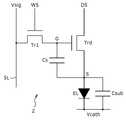
개개의 화소(2)는, 샘플링 트랜지스터(Tr1), 구동 트랜지스터(Trd), 기억 커패시터(storage capacitor; Cs), 서브 커패시터(Csub), 및 발광 소자(EL)로 구성되어 있다. 개개의 발광 소자(EL)는 RGB 삼원색의 어느 하나의 색으로 발광하도록 되어 있다. 적색 발광 소자를 구비하는 화소(RED)와 녹색 발광 소자를 구비하는 화 소(GREEN)와 청색 발광 소자를 구비하는 화소(BLUE)로 화소 트리오를 구성하고 있다. 이 화소 트리오를 화소 어레이 블록(1)상에서 매트릭스 형상으로 배열함에 의해 컬러 표시를 할 수가 있다.Each
도 2는, 도 1에 도시한 표시 장치에 포함되는 화소(2)의 구체적인 구성 및 결선 관계를 도시하는 회로도이다. 도시하는 바와 같이, 이 화소(2)는, 유기 EL 디바이스 등으로 대표되는 발광 소자(EL)와, 샘플링 트랜지스터(Tr1)와, 구동 트랜지스터(Trd)와, 기억 커패시터(Cs)를 포함한다. 샘플링 트랜지스터(Tr1)의 게이트는 주사선(WS)에 접속되고, 소스 및 드레인의 한쪽은 대응하는 신호선(SL)에 접속되고, 다른쪽은 구동 트랜지스터(Trd)의 게이트(G)에 접속된다. 구동 트랜지스터(Trd)의 소스(S)는 발광 소자(EL)에 접속되고, 드레인은 대응하는 급전선(DS)에 접속된다. 발광 소자(EL)의 캐소드는 접지 전위(Vcath)에 접속되어 있다. 또한 이 접지 배선은 모든 화소(2)에 대해 공통으로 배선되어 있다. 기억 커패시터(화소 커패시터)(Cs)는, 구동 트랜지스터(Trd)의 소스(S)와 게이트(G) 사이에 접속하고 있다. 또한, 발광 소자(EL)와 병렬로 서브 커패시터(Csub)가 접속되어 있다. 이 서브 커패시터(Csub)는 필요에 따라 부가되는 것으로, 기억 커패시터(Cs)에 대한 영상 신호(Vsig)의 입력 게인을 높이는 기능을 갖는다.FIG. 2 is a circuit diagram showing a specific configuration and wiring relationship of the
도 2에 도시한 화소 구성은 한 예로서, 본 발명은 이 회로 구성으로 한정되는 것이 아니다. 기본적으로 각 화소(2)는, 적어도 샘플링 트랜지스터(Tr1)와 구동 트랜지스터(Trd)와 발광 소자(EL)와 기억 커패시터(Cs)를 포함한다. 샘플링 트랜지스터(Tr1)는, 그 제어 단자(게이트)가 주사선(WS)에 접속되고, 그 한 쌍의 전류 단 자(소스 및 드레인)가 신호선(SL)과 구동 트랜지스터(Trd)의 제어 단자 사이에 접속된다. 구동 트랜지스터(Trd)는 한 쌍의 전류 단자(소스 및 드레인)의 한쪽이 발광 소자(EL)에 접속하고, 다른쪽이 급전선(DS)에 접속하고 있다. 기억 커패시터(Cs)는, 구동 트랜지스터(Trd)의 제어 단자(게이트(G))와 구동 트랜지스터(Trd)의 한 쌍의 전류 단자(소스 및 드레인)의 하나(소스(S)) 사이에 접속하고 있다.The pixel configuration shown in FIG. 2 is one example, and the present invention is not limited to this circuit configuration. Basically, each
도 3은, 도 2에 도시한 화소(2)의 동작을 설명하는 타이밍 차트이다. 단 이 타이밍 차트는 본 발명의 실시 형태를 나타내는 것이 아니고, 이상적인 동작 상태를 나타내는 제 1 참고예이다. 시간축을 공통으로 하여, 주사선(WS)의 전위 변화, 급전선(DS)의 전위 변화 및 신호선(SL)의 전위 변화를 나타내고 있다. 또한 이들의 전위 변화와 병행하여, 구동 트랜지스터(Trd)의 게이트(G) 및 소스(S)의 변화도 나타내고 있다.FIG. 3 is a timing chart illustrating the operation of the
이 타이밍 차트는, 화소(2)의 동작의 천이(遷移)에 맞추어서 기간을 (0) 내지 (7)까지 편의적으로 구획하고 있다. 우선 발광 기간(0)에서는, 급전선(DS)가 고전위(Vccp)에 있고, 구동 트랜지스터(Trd)가 구동 전류(Ids)를 발광 소자(EL)에 공급하고 있다. 구동 전류(Ids)는 고전위(Vccp)에 있는 급전선(DS)으로부터 구동 트랜지스터(Trd)를 통하여 발광 소자(EL)를 통과하여, 공통 접지 배선(Vcath)에 유입되고 있다.This timing chart conveniently divides the period from (0) to (7) in accordance with the transition of the operation of the
계속해서 기간(1)에 들어가면, 급전선(DS)을 고전위(Vccp)로부터 저전위(Vini)로 전환한다. 이로써 급전선(DS)은 Vini까지 방전되고, 또한 구동 트랜지스터(Trd)의 소스 전위는 Vini에 가까운 전위까지 천이한다. 급전선(DS)의 배선 용 량이 큰 경우는 비교적 빠른 타이밍에서 급전선(DS)을 고전위(Vccp)로부터 저전위(Vini)로 전환하면 좋다.Subsequently, when the
다음에 기간(2)으로 진행하면, 주사선(WS)을 저레벨(level)로부터 고레벨(level)로 점환함으로써, 샘플링 트랜지스터(Tr1)가 도통 상태가 된다. 이때, 신호선(SL)은 기준 전위(Vofs)에 있다. 따라서 구동 트랜지스터(Trd)의 게이트 전위는 도통한 샘플링 트랜지스터(Tr1)를 통해 신호선(SL)의 기준 전위(Vofs)가 된다. 이와 동시에 구동 트랜지스터(Trd)의 소스 전위는 저전위(Vini)로 고정된다. 이상에 의해 구동 트랜지스터(Trd)의 소스 전위가 영상 신호선(SL)의 기준 전위(Vofs)보다 충분히 낮은 전위(Vini)로 초기화(리셋)된다. 구체적으로는, 구동 트랜지스터(Trd)의 게이트-소스 전압(Vgs)(게이트 전위와 소스 전위의 차)이 구동 트랜지스터(Trd)의 임계 전압(Vth)보다 커지도록, 급전선(DS)의 저전위(Vini)를 설정한다.When the process proceeds to the
이상의 설명으로부터 분명한 바와 같이, 기간(1)과 기간(2)이 임계 전압 보정 동작의 준비 과정으로 되어 있다. 즉 이 준비 과정에서는, 구동 트랜지스터(Trd)의 게이트(G)인 제어 단자를 기준 전위(Vofs)로 유지하는 한편, 구동 트랜지스터(Trd)의 소스(S)가 되는 전류 단자의 사이의 게이트-소스 전압(Vgs)을 임계 전압(Vth)보다 크게 설정하여, 구동 트랜지스터(Trd)를 온 상태로 한다.As is clear from the above description, the
다음에 Vth 캔슬 기간(3)으로 진행하면, 급전선(DS)이 저전위(Vini)로부터 고전위(Vccp)로 천이하고, 구동 트랜지스터(Trd)의 소스 전위가 상승을 시작한다. 구동 트랜지스터(Trd)의 게이트-소스 전압(Vgs)이 임계 전압(Vth)에 도달하면, 전류가 컷오프된다. 이와 같이 하여 구동 트랜지스터(Trd)의 임계 전압(Vth)에 상당 하는 전압이 기억 커패시터(화소 커패시터)(Cs)에 기록된다. 이것이 임계 전압 보정 동작이다. 이때 전류가 오로지 기억 커패시터(Cs)측으로 흐르고, 발광 소자(EL)측으로는 흐르지 않도록 하기 위해, 발광 소자(EL)가 컷오프가 되도록 공통 접지 배선(Vcath)의 전위를 미리 설정하여 둔다.When the process proceeds to the Vth cancel
이상의 설명으로부터 분명한 바와 같이, 이 Vth 캔슬 기간(3)이 임계 전압 보정 동작의 통전 과정(energizing process)으로 되어 있다. 이 통전 과정에서는, 게이트(G)를 기준 전위(Vofs)로 유지한 채로 구동 트랜지스터(Trd)를 통전하고, 구동 트랜지스터(Trd)가 컷오프되면, 그 게이트-소스 사이에 나타나는 임계 전압에 상당하는 전압을 기억 커패시터(Cs)에 보존한다.As is apparent from the above description, this
다음에, 기간(4)으로 진행하면, 주사선(WS)이 저전위측으로 천이하고, 샘플링 트랜지스터(Tr1)가 일단 오프 상태가 된다. 이때 구동 트랜지스터(Trd)의 게이트(G)는 플로팅이 되는데, 게이트-소스 전압(Vgs)은 구동 트랜지스터(Trd)의 임계 전압(Vth)과 동등하기 때문에 컷오프 상태이고, 드레인 전류(Ids)는 흐르지 않는다. 단 이것은 이상 상태이고, 실제로는 구동 트랜지스터(Trd)에 전류 리크가 있기 때문에, 약간이기는 하지만 드레인 전류(Ids)가 흐른다. 이로써 구동 트랜지스터(Trd)의 소스 전위가 변동하고, 이에 수반하여 플로팅 상태에 있는 게이트(G)의 전위도 변동하는, 이른바 부트 스트랩 현상이 생긴다.Subsequently, when the
계속해서 기간(5)으로 진행하면, 신호선(SL)의 전위가 기준 전위(Vofs)로부터 샘플링 전위(신호 전위)(Vsig)로 천이한다. 이로써 다음의 샘플링 동작 및 이동도 보정 동작(신호 기록 및 이동도(μ) 캔슬)의 준비가 완료된다.Subsequently, the
신호 기록/이동도(μ) 캔슬 기간(6)에 들어가면, 주사선(WS)이 고전위측으로 천이하여 샘플링 트랜지스터(Tr1)가 온 상태가 된다. 따라서 구동 트랜지스터(Trd)의 게이트 전위는 신호 전위(Vsig)가 된다. 여기서 발광 소자(EL)는 처음에 컷오프 상태(하이 임피던스 상태)에 있기 때문에, 구동 트랜지스터(Trd)의 드레인-소스 전류(Ids)는 발광 소자 용량 및 서브 커패시터(Csub)에 유입되고, 충전을 시작한다. 따라서 구동 트랜지스터(Trd)의 소스 전위는 상승을 시작하고, 이윽고 구동 트랜지스터(Trd)의 게이트-소스 전압(Vgs)은 Vsig+Vth-△V가 된다. 이와 같이 하여, 신호 전위(Vsig)의 샘플링과 보정량(△V)의 조정이 동시에 행하여진다. Vsig가 높을수록 Ids는 커지고, △V의 절대치도 커진다. 따라서 발광 휘도 레벨에 따른 이동도 보정이 행하여진다. Vsig를 일정하게 한 경우, 구동 트랜지스터(Trd)의 이동도(μ)가 클수록 △V의 절대치가 커진다. 환언하면 이동도(μ)가 클수록 부귀환량(負歸還量)(△V)이 커지기 때문에, 화소마다의 이동도(μ)의 편차를 제거할 수 있다.When the signal write / mobility (μ)
최후로 발광 기간(7)이 되면, 주사선(WS)이 저전위측으로 천이하고, 샘플링 트랜지스터(Tr1)는 오프 상태가 된다. 이로써 구동 트랜지스터(Trd)의 게이트(G)는 신호선(SL)으로부터 분리된다. 동시에 드레인 전류(Ids)가 발광 소자(EL)를 흐르기 시작한다. 이로써 발광 소자(EL)의 애노드 전위는 구동 전류(Ids)에 따라 상승한다. 발광 소자(EL)의 애노드 전위의 상승은, 즉 구동 트랜지스터(Trd)의 소스 전위의 상승과 다름없다. 구동 트랜지스터(Trd)의 소스 전위가 상승하면, 기억 커패시터(Cs)의 부트 스트랩 동작에 의해, 구동 트랜지스터(Trd)의 게이트 전위도 연동하여 상승한다. 게이트 전위의 상승량은 소스 전위의 상승량과 동등하게 된다. 때문 에 발광 기간(7)중 구동 트랜지스터(Trd)의 게이트-소스 전압(Vgs)은 Vsig+Vth-△V로 일정하게 유지된다. 또한 이상의 설명에서는, Vofs=Vcath=0V로 하여 Vgs를 계산하고 있다.At the end of the
도 4는, 도 1 및 도 2에 도시한 표시 장치의 동작을 설명하는 타이밍 차트이다. 이 타이밍 차트는 이상 상태에서 빗나간 실제의 게이트(G) 및 소스(S)의 전위 변화를 나타내고 있고, 제 2 참고예이다. 이해를 용이하게 하기 위해, 도 3에 도시한 제 1 참고예와 같은 표기를 채용하고 있다. 도시하는 바와 같이 실제의 동작을 나타내는 이 제 2 참고예에서도, Vth 캔슬 기간(3)에서 통전 과정을 수행한 후, 제어 신호(WS)를 하강시켜 샘플링 트랜지스터(Tr1)를 오프 하는데, 이로써 구동 트랜지스터(Trd)의 게이트(G)가 일시적으로 신호선에서 분리되기 때문에, 플로팅 상태가 된다. 그 때 샘플링 트랜지스터(Tr1)의 스위칭에 의해 게이트(G)에 커플링이 들어가기 때문에, 게이트(G)의 전위도 변동한다. 이에 따라 소스(S)의 전위도 변동한다. 더하여 개개의 화소의 구동 트랜지스터(Trd)의 특성에 편차가 있기 때문에, 리크 전류가 구동 트랜지스터(Trd)의 드레인/소스 사이에 흐른다. 이 리크의 영향으로 플로팅 기간(4)에서는 소스 전위가 상승하여 간다. 이에 수반하여 게이트(G)의 전위도 상승하여 간다. 이른바 부트 스트랩과 같은 현상이 이 플로팅 기간(4)에서 생기고 있다.4 is a timing chart illustrating the operation of the display device shown in FIGS. 1 and 2. This timing chart shows the actual change of the potentials of the gate G and the source S which are missed in the abnormal state, and is a second reference example. For ease of understanding, the same notation as that of the first reference example shown in FIG. 3 is employed. Also in this second reference example showing actual operation as shown in the drawing, after conducting an energization process in the
이 후 기록 기간(6)이 되면 제어 신호가 재차 주사선(WS)에 인가되고, 샘플링 트랜지스터(Tr1)가 온 하고, 구동 트랜지스터(Trd)의 게이트(G)에 신호 전위(Vsig)가 기록된다. 이때 소스(S)의 전위도 약간 상승하여 기록 기간(6)이 끝난 시점에서는, X로 나타내는 소스 전위로 되어 있다. 여기서 플로팅 기간(4)을 통하여 소스 전위(S) 및 게이트 전위(G)는 리크의 영향으로 상승하고 있기 때문에, 기록 기간(6)이 끝난 시점에서의 소스 전위(S)는 반드시는 일정하지가 않고, 개개의 화소에서 다르다. 이 때문에 기록 기간(6)이 완료된 시점에서 구동 트랜지스터(Trd)의 소스-게이트 전압(Vgs)은 화소마다 변동, 발광 휘도에 차가 생긴다. 일반적으로 구동 트랜지스터(Trd)의 리크의 경향은 주사선(WS)(라인)에 따라 나타나기 때문에, Vgs의 편차는 발광시 수평 방향의 줄무늬 얼룩이 되어 화면의 균일성을 손상시켜 버린다. 표시 장치의 고정밀화에 의해 화소 어레이부의 화소 총수가 증가하면, 그만큼 수평 주사 기간이 짧아지고, Vth 캔슬 기간(3)을 충분히 확보할 수가 없다. 따라서 구동 트랜지스터(Trd)의 Vth의 편차가 충분히 캔슬되지 않는 상태가 된다. 게다가 개개의 구동 트랜지스터(Trd)의 리크의 편차의 영향이 더해지면, Vgs가 크게 흐트러지고, 줄무늬 얼룩이 악화하여 버린다.After the
도 5는, 도 1 및 도 2에 도시한 표시 장치의 동작을 설명하는 타이밍 차트이다. 이 타이밍 차트는 본 발명의 실시 형태를 나타내고 있고, 이해를 용이하게 하기 위해 도 3 및 도 4에 도시한 참고예와 같은 표기를 채용하고 있다. 도시하는 바와 같이, 본 발명에서는 Vth 보정 기간(3)의 통전 과정을 경과한 후, 플로팅 기간(4)으로 진행하기 전에 기간(3a)을 삽입하고, 여기서 압축 과정을 수행하고 있다. 이 압축 과정에서는, 구동 트랜지스터(Trd)의 게이트(G)에 인가되고 있는 기준 전위(Vofs)를 바꾸어, 게이트-소스 전압(Vgs)을 임계 전압(Vth)에 상당하는 전압보다도 압축하여, 구동 트랜지스터(Trd)를 확실하게 오프 하고 있다. 구체적으로는, 이 압축 과정(3a)에서는, 급전선(DS)을 고전위(Vccp)에 유지한 채로 라이트 스캐너가 제어 신호를 해제하여 샘플링 트랜지스터(Tr1)를 오프 하기 직전에, 신호 드라이버가 기준 전위(Vofs)의 레벨을 Vofs1로부터 Vofs2로 하방 전환한다. 즉 Vth 캔슬 기간(3)의 종료 직전에, 신호선(SL)에 인가하고 있는 기준 전위(Vofs1)를, 구동 트랜지스터(Trd)의 Vth가 컷인(cut in)되는 레벨(Vofs2)까지 저하시킨다. 이로써 Vgs가 Vth보다 작아지기 때문에, 구동 트랜지스터(Trd)의 전류 리크를 억제할 수 있다. 따라서 구동 트랜지스터(Trd)의 소스 전위는 플로팅 기간(4) 중 변동하는 일이 없고, 구동 트랜지스터의 리크 전류의 편차에 기인하는 발광 휘도의 얼룩을 억제할 수 있다.FIG. 5 is a timing chart for explaining the operation of the display device shown in FIGS. 1 and 2. This timing chart shows an embodiment of the present invention and employs the same notation as in the reference example shown in Figs. 3 and 4 in order to facilitate understanding. As shown in the figure, in the present invention, after passing the energization process of the
////또한 압축 과정(3a)에서 신호선(SL)을 기준 전위(Vofs1)로부터 Vofs2로 저하시킬 때, 급격한 전압 변동은 소스(S)에의 커플링을 일으키고 Vgs가 오픈(open)될 가능성이 있다. 이 경우에는 커플링을 일으키지 않을 정도로 트랜지언트를 스무스(smooth)하게 하면 좋다. 트랜지언트를 스무스하게 하는 수법으로서는, 샘플링 트랜지스터(Tr1)의 게이트에 인가하는 제어 신호 펄스의 하강을 스무스하게하는 방법이 있다. 예를 들면 라이트 스캐너의 최종단 버퍼를 구성하는 N채널 트랜지스터의 사이즈를 작게 설계함으로써, 게이트 펄스의 하강을 스무스하게 할 수 있다. 또는 신호 드라이버의 출력 버퍼에 접속하고 있는 전원에 하강을 스무스하게 한 기준 전위(Vofs)의 파형을 공급하는 것이라도 좋다. 이와 같이 본 발명에서는 샘플링 트랜지스터(Tr1)가 온 하고 있는 기준 전위 기록 기간(준비 기간(2)과 Vth 캔슬 기간(3))에서, 구동 트랜지스터(Trd)의 게이트(G)에는 신호선에서 공급된 기 준 전위(Vofs1)가 인가되고 있다. 이 기준 전위 기록 기간의 최종 단계에서는, 구동 트랜지스터(Trd)의 게이트-소스 전압(Vgs)는 Vth로 되어 있다. 이 기준 전위 기록 기간이 종료하기 직전에 기준 전위(Vofs1)를 Vofs2로 하방 전환하고, Vgs를 압축한다. 이로써 구동 트랜지스터(Trd)는 완전히 오프 상태로 되기 때문에, 플로팅 기간(4)에서는 리크 전류가 흐르는 일이 없고, 구동 트랜지스터(Trd)의 소스(S)의 전위는 안정되어 있다.//// Also, when the signal line SL is lowered from the reference potential Vofs1 to Vofs2 in the
이후 신호 전위 기록 기간(6)이 되면 재차 제어 신호가 주사선(WS)에 인가되고, 샘플링 트랜지스터(Tr1)가 온 한다. 이 시점에서 신호선(SL)은 신호 전위(Vsig)로 전환되어 있기 때문에, 구동 트랜지스터(Trd)의 게이트(G)에는 Vsig가 기록된다. 이때 구동 트랜지스터(Trd)에 흐르는 드레인 전류(Ids)의 일부가 기억 커패시터에 부귀환되기 때문에, 구동 트랜지스터(Trd)의 소스(S)의 전위는 도시하는 바와 같이 X까지 상승한다. 전위(X)는 리크의 영향이 제외되어 있기 때문에 화소 사이에서 흐트러지는 일이 없고, Vgs는 일정하게 유지되고 발광 휘도의 얼룩을 없앨 수 있다.Then, when the signal
도 6은, 도 1에 도시한 표시 장치에 포함되는 수평 실렉터(신호 드라이버)(3)의 구성예를 도시하는 모식적인 회로도이다. 이 신호 드라이버(3)는 복수의 데이터선(Data1, Data2, Data3 …)을 구비하고 있고, 선순차로 1라인분의 데이터를 일제히 열형상의 신호선(SL)에 공급하고 있다. 도시한 예는, 1개의 데이터선(Data)에 3개의 신호선(SL)이 선택 스위치(SEL1, SEL2, SEL3)를 통하여 접속하고 있고, 1개의 데이터선(Data)에 공급된 신호 전위를 시분할로 3개의 신호선(SL)에 공급하는 구성으로 되어 있다.FIG. 6 is a schematic circuit diagram illustrating a configuration example of the horizontal selector (signal driver) 3 included in the display device shown in FIG. 1. The
열형상의 신호선(SL)과 교차하도록 제어선(GOFS)과 전위선(VOFS)이 행형상(라인형상)으로 배치되어 있다. 전위선(VOFS)과 각 신호선(SL)은 스위치(SW)로 접속되어 있다. 이 스위치(SW)는 제어선(GOFS)에 인가되는 제어 신호에 의해 온/오프 제어된다. 각 신호선(SL)에 접속하고 있는 복수의 화소는 용량(C)과 저항(R)으로 모식적으로 표시되어 있다.The control line GOFS and the potential line VOFS are arranged in a row (line shape) so as to intersect the columnar signal lines SL. The potential line VOFS and each signal line SL are connected by a switch SW. This switch SW is controlled on / off by a control signal applied to the control line GOFS. The plurality of pixels connected to each signal line SL is typically represented by a capacitor C and a resistor R. FIG.
도 7은, 도 6에 도시한 신호 드라이버(수평 실렉터)(3)의 동작을 설명하는 타이밍 차트이다. 3개1조(組)의 선택 스위치(SEL1, SEL2, SEL3)에 인가되는 제어 신호를 같은 참조 부호(SEL1, SEL2, SEL3)로 나타내고 있다. 마찬가지로 제어선(GOFS)에 인가되는 제어 신호를 같은 참조 부호(GOFS)로 나타내고 있다. 또한 전위선(VOFS)의 전위는 Vofs2로 고정되어 있다. 더하여 본 신호 드라이버(3)는 약 240개의 데이터선을 구비하고 있고, 각 데이터선에 인가되는 데이터(신호 전위)를 Data1 내지 Data240으로 나타내고 있다. 또한, 신호 드라이버(3)의 동작에는 직접 관계 없지만, 라이트 스캐너측의 동작을 제어하는 타이밍 신호(WSEN1 및 WSEN2)도 시간축을 갖추고 타이밍 차트(7)에 나타내고 있다. 타이밍 신호(WSEN1)는 도 5에 도시한 기준 전위 기록 기간을 규정하고 있다. 타이밍 신호(WSEN2)는 마찬가지로 도 5에 도시한 신호 기록 기간을 규정하고 있다.FIG. 7 is a timing chart illustrating the operation of the signal driver (horizontal selector) 3 shown in FIG. 6. The control signals applied to the three sets of selection switches SEL1, SEL2, and SEL3 are indicated by the same reference numerals SEL1, SEL2, and SEL3. Similarly, the control signal applied to the control line GOFS is indicated by the same reference numeral GOFS. The potential of the potential line VOFS is fixed at Vofs2. In addition, the
타이밍 신호(WSEN1)가 하이 레벨이 되어 기준 전위 기록 기간으로 들어간다. 이때 각 데이터선(Data)에 인가되는 전위는 신호 전위로부터 기준 전위(Vofs1)로 전환된다. 동시에 선택 신호(SEL1, SEL2, SEL3)가 일제히 하이 레벨이 된다. 선택 스위치(SEL1, SEL2, SEL3)가 동시에 온 하고, 데이터선(Data)에 인가된 기준 전위(Vofs1)는 3개의 신호선(SL)에 출력된다. 따라서 기준 전위 기록 기간에는, 열형상의 신호선(SL)에 일제히 기준 전위(Vofs1)가 기록되게 된다.The timing signal WSEN1 goes high and enters the reference potential write period. At this time, the potential applied to each data line Data is switched from the signal potential to the reference potential Vofs1. At the same time, the selection signals SEL1, SEL2, and SEL3 all go to the high level. The selection switches SEL1, SEL2, and SEL3 are turned on at the same time, and the reference potential Vofs1 applied to the data line Data is output to the three signal lines SL. Therefore, in the reference potential writing period, the reference potential Vofs1 is simultaneously recorded in the columnar signal lines SL.
그 후 WSEN1이 하이 레벨로부터 로우 레벨로 전환하기 직전, 제어 신호(GOFS)가 하이 레벨이 되고, 스위치(SW)가 일제히 온 한다. 이 시점에서 실렉터1, 실렉터2, 실렉터3은 이미 오프 하고 있다. 전위선(VOFS)의 전위(Vofs2)가 스위치(SW)를 통하여 각 신호선(SL)에 기록된다. 이상에 의해 기준 전위 기록 기간이 종료되기 직전에 각 신호선(SL)의 전위가 Vofs1로부터 Vofs2로 하방 전환되고, 전술한 Vgs의 압축 과정을 실현할 수 있다.Then, just before WSEN1 switches from the high level to the low level, the control signal GOFS goes to the high level, and the switch SW is turned on all at once. At this point,
이 후 각 데이터선(Data)에는 소정의 신호 전위가 공급된다. 이에 동기하여 선택 신호(SEL1, SEL2, SEL3)가 시분할적으로 하이 레벨이 되고, 대응하는 신호 전위가 대응하는 신호선(SL)에 기록되어 간다. 계속해서 타이밍 신호(WSEN2)가 하이 레벨이 되면, 신호 전위 기록 기간으로 들어가고, 1라인분의 화소의 샘플링 트랜지스터가 일제히 온 한다. 이로써 각 신호선(SL)에 인가되어 있던 신호 전위가 1라인분의 화소에 샘플링 되고, 선순차 기록 동작이 행하여진다.Thereafter, a predetermined signal potential is supplied to each data line Data. In synchronism with this, the selection signals SEL1, SEL2, and SEL3 become time-divisionally high, and corresponding signal potentials are recorded in the corresponding signal lines SL. Subsequently, when the timing signal WSEN2 becomes high, the signal potential write period is entered, and the sampling transistors of one line of pixels are all turned on at the same time. Thereby, the signal potential applied to each signal line SL is sampled to one line of pixels, and a line sequential writing operation is performed.
도 8은, 도 6에 도시한 신호 드라이버(3)의 동작을 설명하는 타이밍 차트이다. 단 이 타이밍 차트는 기준 전위의 전환을 수행하지 않는 참고예를 나타내고 있다. 도시하는 바와 같이 이 참고예에서는 데이터선(Data)에 신호 전위가 공급되는 한편, 전위선(VOFS)에 기준 전위(Vofs)가 공급되고 있다. 타이밍 신호(WSEN1)가 하이 레벨이 되어 기준 전위 기록 기간이 되면, 제어 신호(GOFS)가 하이 레벨이 되 고, 스위치(SW)가 일제히 온 한다. 이 온 한 스위치(SW)를 통하여 전위선(VOFS)의 기준 전위(Vofs)가 열형상의 신호선(SL)에 공급된다. 이상의 설명으로부터 분명한 바와 같이, 이 참고예에서는 기준 전위(Vofs)의 레벨의 전환은 행하여지지 않는다.FIG. 8 is a timing chart for explaining the operation of the
도 9는, 도 1 및 도 2에 도시한 표시 장치의 동작을 설명하는 타이밍 차트이다. 이 타이밍 차트는 제 3 참고예를 나타내고 있고, 이해를 용이하게 하기 위해 도 3 및 도 4에 도시한 앞의 참고예와 같은 표기를 채용하고 있다. 다른 점은, 이 제 3 참고예가 임계 전압 보정 동작 내의 통전 과정을 복수회 반복하여 시분할적으로 행하고 있는 것이다. 일반적으로 화소의 임계 전압 보정 동작, 신호 전위 기록 동작 및 발광 동작은 라인마다 선순차로 행하여진다. 따라서 임계 전압 보정 동작도 1라인당 1수평 주사 주기(1H)로 행하도록 하고 있다. 그러나 화소의 고정밀화가 진행되면 주사선의 갯수(라인수)가 증가하기 때문에, 그만큼 1H 기간이 짧아지고, 충분한 Vth 캔슬 기간을 취할 수가 없게 된다. 그래서 본 참고예와 같이 임계 전압 보정 동작 중 시간이 필요한 통전 과정을 복수의 수평 기간에 걸쳐서 시분할적으로 행하는 경우가 있다. 도 9의 참고예는, Vth 캔슬 동작을 2회 행한 경우이다. 최초의 Vth 캔슬 기간(31)에서 통전 과정을 실행하지만, 시간이 짧기 때문에 Vgs는 아직도 Vth까지 도달하지 않는다. 1회째의 Vth 캔슬 기간(31)이 끝나면 제어 신호를 일단 로우 레벨로 전환하고, 샘플링 트랜지스터(Tr1)를 오프 하여 구동 트랜지스터(Trd)의 게이트(G)를 신호선(SL)으로부터 분리한다. 이로써 구동 트랜지스터(Trd)의 게이트(G)는 플로팅 상태가 된다. 이 플로팅 기간(41)에서는 구동 트랜지스터(Trd)는 오프로 되지 않아 리크 전류가 흐른다. 따라서 소스 전위(S)가 상승 함과 함께 이와 연동하여 게이트(G)의 전위도 상승한다. 이른바 부트 스트랩 현상이 일어난다. 이 전류 리크는 1회째의 Vth 캔슬 기간(31)에서 Vth 캔슬이 불충분할수록 크게 일어난다. 따라서 플로팅 기간(41)이 끝난 시점에서, 구동 트랜지스터(Trd)의 소스 전위는 화소마다 크게 흐트러진다.9 is a timing chart illustrating the operation of the display device shown in FIGS. 1 and 2. This timing chart shows a third reference example and employs the same notation as the previous reference example shown in Figs. 3 and 4 to facilitate understanding. The difference is that this third reference example performs time division by repeating the energization process in the threshold voltage correction operation a plurality of times. In general, the threshold voltage correction operation, the signal potential write operation, and the light emission operation of the pixel are performed line by line in sequence. Therefore, the threshold voltage correction operation is also performed in one
이 후 2회째의 Vth 캔슬 기간(32)이 되면 재차 제어 신호가 하이 레벨이 되고 구동 트랜지스터(Trd)의 게이트(G)에 Vofs가 인가된 상태에서 통전 과정이 행하여진다. 이로써 Vgs는 Vth까지 달한다. 그 후 재차 플로팅 기간(42)으로 진행한 후, 신호 전위 기록 기간(6)에 이르러 구동 트랜지스터(Trd)의 게이트(G)에 신호 전위(Vsig)가 기록되는 한편, 소스 전위도 소정의 레벨까지 상승한다. 그러나, 1회째의 통전 과정에서 Vth 캔슬이 불충분한 경우, 그 후의 플로팅 기간(41)로 전류 리크에 큰 편차가 생기고, 해당 영향이 2회째의 임계 전압 보정 동작에도 악영향을 주고, 결과적으로 신호 전위 기록 기간이 끝난 시점에서 화소마다 Vgs의 편차가 남아 버린다. 이것이 발광시에는 줄무늬 얼룩이 되어 인식된다는 과제가 있다.After that, when the second
도 10은, 도 1 및 도 2에 도시한 표시 장치의 동작을 설명하는 타이밍 차트이다. 이 타이밍 차트는 본 발명의 제 2 실시 형태를 나타내고 있고, 도 9에 도시한 제 3 참고예의 문제점에 대처한 것이다. 이 제 2 실시 형태는 임계 전압 보정 동작을 시분할적으로 행하고 있고, 1회째의 통전 과정(31)과 2회째의 통전 과정(32)을 시간을 띠우고 행하고 있다. 본 발명의 특징 사항으로서, 1회째의 Vth 캔슬 기간(31)에서 이용하는 기준 전위(Vofs1)와, 2회째의 Vth 캔슬 기간(32)에서 이용하는 기준 전위(Vofs2)가 서로 다르도록 하고 있다. 구체적으로는, 제 1 Vth 캔 슬 기간(31)에서 구동 트랜지스터(Trd)의 게이트(G)에 인가하는 기준 전위(Vofs1)는, 2회째의 Vth 보정 기간(32)에서 게이트에 기록하는 기준 전위(Vofs2)보다도 낮게 설정하고 있다. 이로써 1회째의 Vth 캔슬 기간(31)이 불충분하게 끝난 때, Vgs가 넓게 펴저 있는 것이 원인으로 일어나는 구동 트랜지스터(Trd)의 전류 리크를, 미리 Vofs1을 낮게 설정하여 Vgs를 줄여 둠에 의해 해소 또는 경감할 수 있다. 일반적으로 Vth 캔슬 동작을 n회 행하는 경우에는, 1회째의 Vth 캔슬에서 이용하는 Vofs를 가장 저전압으로 하고, 2회째, 3회째 … n회째의 순서로 Vofs를 높게 하든지, 또는 적어도 이전의 전압과 동등하게 하면 좋다. 이러한 수법에 의해 Vth 캔슬 후 플로팅 기간에 생기는 전류 리크를 억제하는 것이 가능해진다.FIG. 10 is a timing chart illustrating the operation of the display device shown in FIGS. 1 and 2. This timing chart shows the second embodiment of the present invention and addresses the problems of the third reference example shown in FIG. In this second embodiment, the threshold voltage correction operation is time-divisionally performed, and the
도 11은, 본 발명에 관한 표시 장치의 다른 실시 형태를 도시하는 블록도이다. 도시하는 바와 같이, 본 표시 장치는 기본적으로 화소 어레이 블록(1)와 스캐너부와 신호부로 구성되어 있다. 화소 어레이 블록(1)는, 행형상으로 배치된 제 1 주사선(WS), 제 2 주사선(AZ1), 제 3 주사선(AZ2) 및 제 4 주사선(DS)과, 열형상으로 배치된 신호선(SL)과, 이들의 주사선(WS, AZ1, AZ2, DS) 및 신호선(SL)에 접속한 행렬형상의 화소 회로(2)와, 각 화소 회로(2)의 동작에 필요한 제 1 전위(Vss1), 제 2 전위(Vss2) 및 제 3 전위(Vcc)를 공급하는 복수의 급전선으로 이루어진다. 신호부는 수평 실렉터(3)로 이루어지고, 신호선(SL)에 영상 신호를 공급한다. 스캐너부는, 라이트 스캐너(4), 드라이브 스캐너(5), 제일 보정용 스캐너(71) 및 제 2 보정용 스캐너(72)로 이루어지고, 각각 제 1 주사선(WS), 제 4 주사선(DS), 제 2 주사선(AZ1) 및 제 3 주사선(AZ2)에 제어 신호를 공급하여 순차적으 로 행마다 화소 회로를 주사한다.11 is a block diagram showing another embodiment of the display device according to the present invention. As shown in the drawing, the present display device basically comprises a
도 12는, 도 11에 도시한 표시 장치에 편입되는 화소 회로의 구성예를 도시하는 회로도이다. 도시하는 바와 같이 화소 회로(2)는, 샘플링 트랜지스터(Tr1)와, 구동 트랜지스터(Trd)와, 제 1 스위칭 트랜지스터(Tr2)와, 제 2 스위칭 트랜지스터(Tr3)와, 제 3 스위칭 트랜지스터(Tr4)와, 기억 커패시터(Cs)과, 발광 소자(EL)를 포함한다. 샘플링 트랜지스터(Tr1)는, 소정의 샘플링 기간에 제 1 주사선(WS)으로부터 공급되는 제어 신호에 따라 도통하여 신호선(SL)으로부터 공급된 영상 신호의 신호 전위를 기억 커패시터(Cs)에 샘플링한다. 기억 커패시터(Cs)는, 샘플링된 영상 신호의 신호 전위에 응하여 구동 트랜지스터(Trd)의 게이트(G)에 입력 전압(Vgs)을 인가한다. 구동 트랜지스터(Trd)는, 입력 전압(Vgs)에 따른 출력 전류(Ids)를 발광 소자(EL)에 공급한다. 발광 소자(EL)는, 소정의 발광 기간 중 구동 트랜지스터(Trd)로부터 공급된 출력 전류(Ids)에 의해 영상 신호의 신호 전위에 응한 휘도로 발광한다.FIG. 12 is a circuit diagram illustrating a configuration example of a pixel circuit incorporated in the display device illustrated in FIG. 11. As shown in the drawing, the
제 1 스위칭 트랜지스터(Tr2)는, 샘플링 기간에 앞서서 제 2 주사선(AZ1)으로부터 공급되는 제어 신호에 따라 도통하여 구동 트랜지스터(Trd)의 게이트(G)를 제 1 전위(Vss1)로 설정한다. 제 2 스위칭 트랜지스터(Tr3)는, 샘플링 기간에 앞서서 제 3 주사선(AZ2)으로부터 공급되는 제어 신호에 따라 도통하여 구동 트랜지스터(Trd)의 소스(S)를 제 2 전위(Vss2)로 설정한다. 제 3 스위칭 트랜지스터(Tr4)는, 샘플링 기간에 앞서서 제 4 주사선(DS)으로부터 공급되는 제어 신호에 따라 도통하여 구동 트랜지스터(Trd)를 제 3 전위(Vcc)에 접속하고, 따라서 구동 트랜지스 터(Trd)의 임계 전압(Vth)에 상당하는 전압을 기억 커패시터(Cs)에 보존시켜서 임계 전압(Vth)의 영향을 보정한다. 또한 이 제 3 스위칭 트랜지스터(Tr4)는, 발광 기간에 재차 제 4 주사선(DS)으로부터 공급되는 제어 신호에 따라 도통하여 구동 트랜지스터(Trd)를 제 3 전위(Vcc)에 접속하여 출력 전류(Ids)를 발광 소자(EL)에 흘린다.The first switching transistor Tr2 conducts in accordance with the control signal supplied from the second scanning line AZ1 prior to the sampling period, thereby setting the gate G of the driving transistor Trd to the first potential Vss1. The second switching transistor Tr3 conducts in accordance with the control signal supplied from the third scanning line AZ2 prior to the sampling period to set the source S of the driving transistor Trd to the second potential Vss2. The third switching transistor Tr4 conducts in accordance with the control signal supplied from the fourth scanning line DS prior to the sampling period to connect the driving transistor Trd to the third potential Vcc, and thus the driving transistor ( The voltage corresponding to the threshold voltage Vth of Trd is stored in the storage capacitor Cs to correct the influence of the threshold voltage Vth. In addition, the third switching transistor Tr4 conducts again according to a control signal supplied from the fourth scanning line DS in the light emission period, connects the driving transistor Trd to the third potential Vcc, and outputs the output current Ids. To the light emitting element EL.
이상의 설명으로부터 분명한 바와 같이, 본 화소 회로(2)는, 5개의 트랜지스터(Tr1 내지 Tr4 및 Trd)와 1개의 기억 커패시터(Cs)과 1개의 발광 소자(EL)로 구성되어 있다. 트랜지스터(Tr1 내지 Tr3과 Trd)는 N채널형의 폴리실리콘 TFT이다. 트랜지스터(Tr4)만 P채널형의 폴리실리콘 TFT이다. 단 본 발명은 이것으로 한정되는 것이 아니고, N채널형과 P채널형의 TFT를 적절히 혼재시킬 수 있다. 발광 소자(EL)는 예를 들면 애노드 및 캐소드를 구비한 다이오드형의 유기 EL 디바이스이다. 단 본 발명은 이것에 한정되는 것이 아니고, 발광 소자는 일반적으로 전류 구동으로 발광하는 모든 디바이스를 포함한다.As apparent from the above description, the
도 13은, 도 12에 도시한 표시 장치로부터 화소 회로(2)의 부분만을 취출한 모식도이다. 이해를 용이하게 하기 위해, 샘플링 트랜지스터(Tr1)에 의해 샘플링되는 영상 신호(Vsig)나, 구동 트랜지스터(Trd)의 입력 전압(Vgs) 및 출력 전류(Ids), 나아가서는 발광 소자(EL)가 가지는 용량 성분(Coled) 등을 더하여 기재하고 있다. 또한 3개의 급전선(Vss1, Vss2 및 Vcc)도 더하고 있다. 3개의 전원 중, Vcc와 Vss2는 고정 전원이다. 이것에 대해 구동 트랜지스터(Trd)의 게이트(G)에 기준 전위로서 주어지는 Vss1은 가변 전원이다. 이 가변 전원은 패널의 외부의 모듈 로 이루어지고, 배선을 통하여 각 화소 회로(2)에 소정의 타이밍에서 레벨이 전환되는 기준 전위(Vss1)를 제공하고 있다.FIG. 13 is a schematic diagram in which only a part of the
도 14는, 도 13에 도시한 화소 회로의 타이밍 차트이다. 도 14를 참조하여, 도 13에 도시한 화소 회로의 동작을 구체적으로 설명한다. 도 14는, 시간축(T)에 따라 각 주사선(WS, AZ1, AZ2 및 DS)에 인가되는 제어 신호의 파형을 도시하고 있다. 표기를 간략화하기 위해, 제어 신호도 대응하는 주사선의 부호와 같은 부호로 나타내고 있다. 트랜지스터(Tr1, Tr2, Tr3)는 N채널형이므로, 주사선(WS, AZ1, AZ2)이 각각 하이 레벨일 때 온 하고, 로우 레벨일 때 오프 한다. 한편 트랜지스터(Tr4)는 P채널형이므로, 주사선(DS)이 하이 레벨일 때 오프 하고, 로우 레벨일 때 온 한다. 또한 이 타이밍 차트는, 각 제어 신호(WS, AZ1, AZ2, DS)의 파형과 함께, 구동 트랜지스터(Trd)의 게이트(G)의 전위 변화 및 소스(S)의 전위 변화도 나타내고 있다.FIG. 14 is a timing chart of the pixel circuit shown in FIG. 13. Referring to Fig. 14, the operation of the pixel circuit shown in Fig. 13 will be described in detail. FIG. 14 shows waveforms of control signals applied to the respective scanning lines WS, AZ1, AZ2 and DS along the time axis T. As shown in FIG. In order to simplify the notation, the control signal is also indicated by the same symbol as that of the corresponding scanning line. Since the transistors Tr1, Tr2, and Tr3 are N-channel type, the transistors Tr1, Tr2, and Tr3 are turned on when the scan lines WS, AZ1, and AZ2 are at the high level, and are turned off at the low level. On the other hand, since the transistor Tr4 is of the P-channel type, the transistor Tr4 is turned off when the scan line DS is at a high level and turned on at a low level. This timing chart also shows the waveforms of the control signals WS, AZ1, AZ2, and DS, as well as the potential change of the gate G and the source S of the drive transistor Trd.
도 14의 타이밍 차트에서는 타이밍(T1 내지 T8)까지를 1필드(1f)로 하고 있다. 1필드의 동안에 화소 어레이의 각 행이 1회 순차적으로 주사된다. 타이밍 차트는, 1행분의 화소에 인가되는 각 제어 신호(WS, AZ1, AZ2, DS)의 파형을 나타내고 있다.In the timing chart of FIG. 14, up to timings T1 to T8 is one
해당 필드가 시작되기 전의 타이밍(T0)에서, 모든 제어 신호(WS, AZ1, AZ2, DS)가 로우 레벨에 있다. 따라서 N채널형의 트랜지스터(Tr1, Tr2, Tr3)는 오프 상태에 있는 한편, P채널형의 트랜지스터(Tr4)만 온 상태이다. 따라서 구동 트랜지스터(Trd)는 온 상태의 트랜지스터(Tr4)를 통하여 전원(Vcc)에 접속하고 있기 때문 에, 소정의 입력 전압(Vgs)에 응하여 출력 전류(Ids)를 발광 소자(EL)에 공급하고 있다. 따라서 타이밍(T0)에서 발광 소자(EL)는 발광하고 있다. 이때 구동 트랜지스터(Trd)에 인가되는 입력 전압(Vgs)은, 게이트 전위(G)와 소스 전위(S)의 차로 표시된다.At the timing T0 before the field starts, all control signals WS, AZ1, AZ2, DS are at the low level. Therefore, the N-channel transistors Tr1, Tr2, and Tr3 are in an off state while only the P-channel transistor Tr4 is in an on state. Therefore, since the driving transistor Trd is connected to the power supply Vcc through the transistor Tr4 in the on state, the driving transistor Trd supplies the output current Ids to the light emitting element EL in response to the predetermined input voltage Vgs. have. Therefore, the light emitting element EL emits light at the timing T0. At this time, the input voltage Vgs applied to the driving transistor Trd is represented by the difference between the gate potential G and the source potential S.
해당 필드가 시작되는 타이밍(T1)에서, 제어 신호(DS)가 로우 레벨로부터 하이 레벨로 전환된다. 이로써 트랜지스터(Tr4)가 오프 하고, 구동 트랜지스터(Trd)는 전원(Vcc)으로부터 분리되기 때문에, 발광이 정지하고 비발광 기간으로 들어간다. 따라서 타이밍(T1)에 들어가면, 모든 트랜지스터(Tr1 내지 Tr4)가 오프 상태가 된다.At the timing T1 at which the field starts, the control signal DS is switched from the low level to the high level. As a result, the transistor Tr4 is turned off and the driving transistor Trd is separated from the power supply Vcc, so that light emission stops and enters the non-light emission period. Therefore, when the timing T1 is entered, all the transistors Tr1 to Tr4 are turned off.
계속해서 타이밍(T2)으로 진행하면, 제어 신호(AZ1 및 AZ2)가 하이 레벨이 되기 때문에, 스위칭 트랜지스터(Tr2 및 Tr3)가 온 한다. 이 결과, 구동 트랜지스터(Trd)의 게이트(G)가 기준 전위(Vss1)에 접속하고, 소스(S)가 기준 전위(Vss2)에 접속된다. 여기서 Vss1-Vss2>Vth를 충족시키고 있고, Vss1-Vss2=Vgs>Vth로 함으로써, 그 후 타이밍(T3)에서 행하여지는 Vth 보정의 준비를 행한다. 환언하면 기간(T2 및 T3)은, 구동 트랜지스터(Trd)의 리셋 기간에 상당한다. 또한, 발광 소자(EL)의 임계 전압을 VthEL이라고 하면, VthEL>Vss2로 설정되어 있다. 이로써, 발광 소자(EL)에는 마이너스 바이어스가 인가되고, 이른바 역(逆)바이어스 상태가 된다. 이 역바이어스 상태는, 후에 행하는 Vth 보정 동작 및 이동도 보정 동작을 정상적으로 행하기 위해 필요하다.Subsequently, when the control proceeds to the timing T2, since the control signals AZ1 and AZ2 are at a high level, the switching transistors Tr2 and Tr3 are turned on. As a result, the gate G of the driving transistor Trd is connected to the reference potential Vss1, and the source S is connected to the reference potential Vss2. Here, Vss1-Vss2> Vth is satisfied, and Vss1-Vss2 = Vgs> Vth is prepared to prepare for Vth correction performed at timing T3 thereafter. In other words, the periods T2 and T3 correspond to the reset period of the driving transistor Trd. If the threshold voltage of the light emitting element EL is VthEL, VthEL> Vss2 is set. As a result, a negative bias is applied to the light emitting element EL, so that a so-called reverse bias state is obtained. This reverse bias state is necessary to normally perform the Vth correction operation and the mobility correction operation performed later.
타이밍(T3)에서는 제어 신호(AZ2)를 로우 레벨로 하고, 그 직후, 제어 신 호(DS)도 로우 레벨로 하고 있다. 이로써 트랜지스터(Tr3)가 오프 하는 한편 트랜지스터(Tr4)가 온 한다. 이 결과 드레인 전류(Ids)가 기억 커패시터(Cs)에 유입되고, Vth 보정 동작을 시작한다. 이때 구동 트랜지스터(Trd)의 게이트(G)는 Vss1로 유지되어 있고, 구동 트랜지스터(Trd)가 컷오프할 때까지 전류(Ids)가 흐른다. 컷오프하면 구동 트랜지스터(Trd)의 소스 전위(S)는 Vss1-Vth가 된다. 드레인 전류가 컷오프 한 후의 타이밍(T4)에서 제어 신호(DS)를 재차 하이 레벨에 되돌려서, 스위칭 트랜지스터(Tr4)를 오프 한다. 또한 제어 신호(AZ1)도 로우 레벨로 되돌려서, 스위칭 트랜지스터(Tr2)도 오프 한다. 이 결과, 기억 커패시터(Cs)에 Vth가 유지 고정된다. 이와 같이 타이밍(T3 및 T4)은 구동 트랜지스터(Trd)의 임계 전압(Vth)을 검출하는 기간이다. 여기서는, 이 검출 기간(T3 및 T4)을 Vth 보정 기간이라고 부르고 있다.At the timing T3, the control signal AZ2 is set at the low level, and immediately after that, the control signal DS is also at the low level. As a result, the transistor Tr3 is turned off while the transistor Tr4 is turned on. As a result, the drain current Ids flows into the memory capacitor Cs, and starts the Vth correction operation. At this time, the gate G of the driving transistor Trd is maintained at Vss1, and the current Ids flows until the driving transistor Trd is cut off. When cut off, the source potential S of the driving transistor Trd is Vss1-Vth. At the timing T4 after the drain current cuts off, the control signal DS is returned to the high level again to turn off the switching transistor Tr4. The control signal AZ1 is also returned to the low level, and the switching transistor Tr2 is also turned off. As a result, Vth is held and fixed to the memory capacitor Cs. As described above, the timings T3 and T4 are periods for detecting the threshold voltage Vth of the driving transistor Trd. Here, these detection periods T3 and T4 are called Vth correction periods.
이와 같이 하여 구동 트랜지스터(Trd)의 임계 전압(Vth)을 검출하고 기억 커패시터(Cs)에 기록한 후, 타이밍(T4)에서 구동 트랜지스터(Trd)의 게이트(G)에 인가되고 있는 기준 전위(Vss1)의 레벨을 하방으로 전환한다. 이로써, 구동 트랜지스터(Trd)의 게이트-소스 전압(Vgs)을 Vth 상당의 전압보다도 압축할 수 있다. 이 압축에 의해 구동 트랜지스터(Trd)는 완전히 오프 상태로 되고, 리크 전류가 흐르는 일은 없다. 이 후 제어 신호(AZ1)를 하이 레벨로부터 로우 레벨로 전환하여 스위칭 트랜지스터(Tr2)가 오프 하고, 구동 트랜지스터(Trd)의 게이트(G)는 기준 전위(Vss1)로부터 분리되고, 플로팅 상태가 된다. 이 플로팅 상태가 되어도 구동 트랜지스터(Trd)는 완전히 오프 하고 있기 때문에 리크 전류는 흐르지 않고, 소스 전 위는 일정하게 유지된다. 기억 커패시터(Vgs)에 기록된 임계 전압(Vth)은 Vss1의 레벨 전환에 의해 압축되지만, 이것은 모든 화소에서 공통으로 생기기 때문에 발광 휘도의 편차의 요인으로는 되지 않는다. 역으로 Vgs를 압축함으로써 구동 트랜지스터(Trd)에 리크 전류가 흐르지 않게 되고, 그 편차의 영향을 제거할 수 있다.In this way, the threshold voltage Vth of the driving transistor Trd is detected and written to the storage capacitor Cs, and then the reference potential Vss1 applied to the gate G of the driving transistor Trd at the timing T4. Toggle the level down. Thus, the gate-source voltage Vgs of the driving transistor Trd can be compressed more than the voltage corresponding to Vth. By this compression, the driving transistor Trd is completely turned off, and no leakage current flows. Thereafter, the switching signal Tr2 is turned off by switching the control signal AZ1 from the high level to the low level, and the gate G of the driving transistor Trd is separated from the reference potential Vss1 and is in a floating state. Even in this floating state, since the driving transistor Trd is completely off, the leakage current does not flow and the source potential is kept constant. The threshold voltage Vth recorded in the memory capacitor Vgs is compressed by the level switching of Vss1, but this does not become a factor of the variation in the luminance of light emission since it occurs in common in all pixels. On the contrary, by compressing Vgs, the leakage current does not flow in the driving transistor Trd, and the influence of the deviation can be eliminated.
이와 같이 Vth 보정을 수행한 후 타이밍(T5)에서 제어 신호(WS)를 하이 레벨로 전환하고, 샘플링 트랜지스터(Tr1)를 온 하여 영상 신호(Vsig)를 기억 커패시터(Cs)에 기록한다. 발광 소자(EL)의 등가 용량(Coled)에 비하여 기억 커패시터(Cs)는 충분히 작다. 이 결과, 영상 신호(Vsig)의 거의 대부분이 기억 커패시터(Cs)에 기록된다. 정확하게는, Vss1에 대한 Vsig의 차분(Vsig-Vss1)이 기억 커패시터(Cs)에 기록된다. 따라서 구동 트랜지스터(Trd)의 게이트(G)와 소스(S) 사이의 전압(Vgs)은, 앞서 검출 보존된 Vth와 금회 샘플링된 Vsig-Vss1을 더한 레벨(Vsig-Vss1+Vth)이 된다. 이후 설명 간이화를 위해 Vss1=0V로 하면, 게이트-소스 전압(Vgs)은 도 4의 타이밍 차트에 도시하는 바와 같이 Vsig+Vth가 된다. 이러한 영상 신호(Vsig)의 샘플링은 제어 신호(WS)가 로우 레벨로 되돌아오는 타이밍(T6)까지 행하여진다. 즉 타이밍(T5-T6)이 신호 기록 기간에 상당한다.After the Vth correction is performed, the control signal WS is switched to the high level at the timing T5, the sampling transistor Tr1 is turned on, and the image signal Vsig is written to the memory capacitor Cs. The memory capacitor Cs is sufficiently small compared to the equivalent capacitance Coled of the light emitting element EL. As a result, almost all of the video signal Vsig is recorded in the memory capacitor Cs. To be precise, the difference Vsig to Vss1 (Vsig-Vss1) is recorded in the memory capacitor Cs. Therefore, the voltage Vgs between the gate G and the source S of the driving transistor Trd becomes the level (Vsig-Vss1 + Vth) obtained by adding the previously detected Vth and Vsig-Vss1 sampled this time. In the following description, for the sake of simplicity, when Vss1 = 0V, the gate-source voltage Vgs becomes Vsig + Vth as shown in the timing chart of FIG. The sampling of the video signal Vsig is performed until the timing T6 at which the control signal WS returns to the low level. That is, the timing T5-T6 corresponds to the signal writing period.
계속해서 타이밍(T7)에서 제어 신호(DS)가 로우 레벨이 되고 스위칭 트랜지스터(Tr4)가 온 한다. 이로써 구동 트랜지스터(Trd)가 전원(Vcc)에 접속되기 때문에, 화소 회로는 비발광 기간으로부터 발광 기간으로 진행된다. 그 전의 타이밍(T6)에서 제어 신호(WS)가 로우 레벨이 되고 샘플링 트랜지스터(Tr1)는 이미 오프 하고 있다. 이 때문에 구동 트랜지스터(Trd)의 게이트(G)는 신호선(SL)으로부터 분리되어 있다. 영상 신호(Vsig)의 인가가 해제되어 있기 때문에, 스위칭 트랜지스터(Tr4)의 온과 함께, 구동 트랜지스터(Trd)의 게이트 전위(G)는 상승 가능해지고, 소스 전위(S)와 함께 상승하여 간다. 또한 본 실시 형태의 화소 회로는 구동 트랜지스터(Trd)의 소스와 발광 소자(EL)의 애노드가 접속하고 있다. 그 때문에, 구동 트랜지스터(Trd)의 소스 전위(S)는 동시에 발광 소자(EL)의 애노드 전위(Va)이기도 하다. 도 14의 타이밍 차트는, 이 발광 소자(EL)의 애노드 전위(Va)도 나타내고 있다. 이 발광 기간은 다음의 필드로 들어가기 전의 타이밍(T8)에서 끝난다.Subsequently, at timing T7, control signal DS goes low and switching transistor Tr4 is turned on. As a result, since the driving transistor Trd is connected to the power source Vcc, the pixel circuit proceeds from the non-light emitting period to the light emitting period. At the previous timing T6, the control signal WS is at a low level and the sampling transistor Tr1 is already turned off. For this reason, the gate G of the drive transistor Trd is separated from the signal line SL. Since the application of the video signal Vsig is released, the gate potential G of the driving transistor Trd can be raised with the switching transistor Tr4 turned on, and rises with the source potential S. As shown in FIG. In the pixel circuit of this embodiment, the source of the driving transistor Trd and the anode of the light emitting element EL are connected. Therefore, the source potential S of the drive transistor Trd is also the anode potential Va of the light emitting element EL. The timing chart of FIG. 14 also shows the anode potential Va of this light emitting element EL. This light emission period ends at the timing T8 before entering the next field.
상술한 바와 같이 타이밍(T7)에서는, 구동 트랜지스터(Trd)의 게이트 전위(G)가 상승 가능해지고, 이와 연동하여 소스 전위(S)가 상승하여 간다. 이것이 부트 스트랩 동작이다. 이 부트 스트랩 동작의 동안, 기억 커패시터(Cs)에 보존된 게이트-소스 전압(Vgs)은 (Vsig+Vth)의 값을 유지한다. 즉 이 부트 스트랩 동작은, 기억 커패시터(Cs)로 보존된 Vgs를 일정하게 유지한 채로, 발광 소자(EL)의 애노드 전위(Va)의 상승을 가능하게 하는 것이다. 구동 트랜지스터의 소스 전위(S)의 상승, 즉 발광 소자(EL)의 애노드 전위(Va)의 상승에 수반하여, 발광 소자(EL)의 역바이어스 상태는 해소되기 때문에, 출력 전류(Ids)의 유입에 의해 발광 소자(EL)는 실제로 발광을 시작한다. 이때의 드레인 전류(Ids) 대(對) 게이트 전압(Vgs)의 관계는, 앞서의 트랜지스터 특성 식 1의 Vgs에 Vsig+Vth를 대입함으로써, 이하의 식과 같이 주어진다.As described above, at the timing T7, the gate potential G of the driving transistor Trd can rise, and the source potential S rises in conjunction with this. This is the bootstrap behavior. During this bootstrap operation, the gate-source voltage Vgs stored in the memory capacitor Cs maintains the value of (Vsig + Vth). In other words, this bootstrap operation enables the anode potential Va of the light emitting element EL to rise while the Vgs stored in the memory capacitor Cs are kept constant. With the rise of the source potential S of the driving transistor, that is, the rise of the anode potential Va of the light emitting element EL, the reverse bias state of the light emitting element EL is eliminated, so that the output current Ids flows in. By this, the light emitting element EL actually starts emitting light. The relationship between the drain current Ids and the gate voltage Vgs at this time is given by the following equation by substituting Vsig + Vth in Vgs of the transistor
Ids=k·μ(Vgs-Vth)2=K·μ(Vsig)2Ids = μμ (Vgs-Vth)2 = Kμ (Vsig)2
상기 식에서, k=(1/2)(W/L)Cox이다(W는 트랜지스터의 게이트 폭, L은 게이트 길이, Cox는 게이트 용량). 이 특성식으로부터 Vth의 항이 캔슬되어 있고, 발광 소자(EL)에 공급되는 출력 전류(Ids)는 구동 트랜지스터(Trd)의 임계 전압(Vth)에 의존하지 않는 것을 알 수 있다. 기본적으로 드레인 전류(Ids)는 영상 신호의 신호 전압(Vsig)에 의해 정해진다. 환언하면, 발광 소자(EL)는 영상 신호(Vsig)에 따른 휘도로 발광하게 된다. 더하여 본 화소 회로는 구동 트랜지스터의 소스 전위, 즉 발광 소자의 애노드 전위(Va)에 의존하는 일 없이, 항상 게이트 전압(Vgs)을 일정하게 유지하고 있다. 이 부트 스트랩 기능 때문에, 본 화소 회로는 발광 소자(EL)의 I-V 특성의 경시변동의 영향을 받는 일 없이, 화면 휘도를 안정적으로 유지할 수 있다.In the above formula, k = (1/2) (W / L) Cox (W is the gate width of the transistor, L is the gate length, and Cox is the gate capacitance). It can be seen from this characteristic formula that the term Vth is canceled and the output current Ids supplied to the light emitting element EL does not depend on the threshold voltage Vth of the driving transistor Trd. Basically, the drain current Ids is determined by the signal voltage Vsig of the image signal. In other words, the light emitting element EL emits light with luminance according to the image signal Vsig. In addition, the pixel circuit always maintains the gate voltage Vgs constant regardless of the source potential of the driving transistor, that is, the anode potential Va of the light emitting element. Because of this bootstrap function, the present pixel circuit can stably maintain the screen luminance without being affected by the time-varying variation of the I-V characteristic of the light emitting element EL.
본 발명에 관한 표시 장치는, 도 15에 도시하는 바와 같은 박막 디바이스 구성을 갖는다. 본 도면은, 절연성의 기판에 형성된 화소의 모식적인 단면 구조를 나타내고 있다. 도시하는 바와 같이, 화소는, 복수의 박막 트랜지스터를 포함하는 트랜지스터부(도면에서는 1개의 TFT를 예시), 기억 커패시터 등의 용량부 및 유기 EL 소자 등의 발광부를 포함한다. 기판의 위에 TFT 프로세스로 트랜지스터부나 용량부가 형성되고, 그 위에 유기 EL 소자 등의 발광부가 적층되어 있다. 그 위에 접착제를 통하여 투명한 대향 기판을 부착하여 플랫 패널로 하고 있다.The display device according to the present invention has a thin film device configuration as shown in FIG. 15. This figure shows the typical cross-sectional structure of a pixel formed on an insulating substrate. As shown in the drawing, the pixel includes a transistor section (a TFT is illustrated in the drawing) including a plurality of thin film transistors, a capacitor section such as a storage capacitor, and a light emitting section such as an organic EL element. A transistor portion and a capacitor portion are formed on the substrate by a TFT process, and light emitting portions such as an organic EL element are stacked thereon. The transparent opposing board | substrate was affixed on it through the adhesive agent, and it is set as a flat panel.
본 발명에 관한 표시 장치는, 도 16에 도시하는 바와 같이 플랫형의 모듈 형상의 것을 포함한다. 예를 들면, 절연성의 기판상에, 유기 EL 소자, 박막 트랜지스터, 박막 용량 등으로 각각 이루어지는 화소를 매트릭스 형상으로 집적 형성한 화 소 어레이부를 마련하고, 이 화소 어레이부(화소 매트릭스부)를 둘러싸도록 접착제를 배치하고, 유리 등의 대향 기판을 부착하여 표시 모듈로 한다. 이 투명한 대향 기판에는 필요에 따라, 컬러 필터, 보호막, 차광막 등을 마련하여도 좋다. 표시 모듈에는, 외부에서 화소 어레이부에의 신호 등을 입출력하기 위한 커넥터로서 예를 들면 FPC(Flexible Printed Circuit)를 마련하여도 좋다.The display device according to the present invention includes a flat modular shape as shown in FIG. 16. For example, on an insulating substrate, a pixel array portion in which pixels each formed of an organic EL element, a thin film transistor, a thin film capacitor, or the like are integrally formed in a matrix form is provided to surround the pixel array portion (pixel matrix portion). An adhesive agent is arrange | positioned, and opposing board | substrates, such as glass, are attached and it is set as a display module. In this transparent counter substrate, you may provide a color filter, a protective film, a light shielding film, etc. as needed. In the display module, for example, a flexible printed circuit (FPC) may be provided as a connector for inputting and outputting signals and the like to the pixel array unit from the outside.
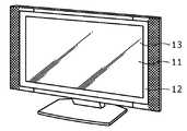
이상 설명한 본 발명에서의 표시 장치는, 플랫 패널 형상을 가지며, 다양한 전자기기, 예를 들면, 디지털 카메라, 노트형 퍼스널 컴퓨터, 휴대 전화, 비디오 카메라 등, 전자기기에 입력된, 또는, 전자기기 내에서 생성한 구동 신호를 화상 또는 영상으로서 표시하는 모든 분야의 전자기기의 디스플레이에 적용하는 것이 가능하다. 이하 이와 같은 표시 장치가 적용된 전자기기의 예를 나타낸다.The display device according to the present invention described above has a flat panel shape and is input to an electronic device, such as a digital camera, a notebook computer, a mobile phone, a video camera, or in an electronic device. It is possible to apply to the display of electronic devices of all fields to display the drive signal generated in the image or image. Hereinafter, an example of an electronic device to which such a display device is applied will be described.
도 17은 본 발명이 적용된 텔레비전이고, 프런트 패널(12), 필터 유리(13) 등으로 구성되는 영상 표시 화면(11)을 포함하고, 본 발명의 표시 장치를 그 영상 표시 화면(11)에 이용함에 의해 제작된다.Fig. 17 is a television to which the present invention is applied and includes a
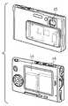
도 18은 본 발명이 적용된 디지털 카메라이고, 위가 정면도이고 아래가 배면도이다. 이 디지털 카메라는, 촬상 렌즈, 플래시용의 발광부(15), 표시부(16), 컨트롤 스위치, 메뉴 스위치, 셔터(19) 등을 포함하고, 본 발명의 표시 장치를 그 표시부(16)에 이용함에 의해 제작된다.18 is a digital camera to which the present invention is applied, and a top view is a front view and a bottom view is a rear view. This digital camera includes an imaging lens, a
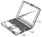
도 19는 본 발명이 적용된 노트형 퍼스널 컴퓨터이고, 본체(20)에는 문자 등을 입력할 때 조작되는 키보드(21)를 포함하고, 본체 커버에는 화상을 표시하는 표시부(22)를 포함하고, 본 발명의 표시 장치를 그 표시부(22)에 이용함에 의해 제작 된다.Fig. 19 is a notebook personal computer to which the present invention is applied, the
도 20은 본 발명이 적용된 휴대 단말 장치이고, 왼쪽이 열려진 상태를 도시하고, 오른쪽이 닫혔던 상태를 도시하고 있다. 이 휴대 단말 장치는, 상측 몸체(23), 하측 몸체(24), 연결부(여기서는 힌지부)(25), 디스플레이(26), 서브디스플레이(27), 픽처 라이트(28), 카메라(29) 등을 포함하고, 본 발명의 표시 장치를 그 디스플레이(26)이나 서브디스플레이(27)에 이용함에 의해 제작된다.20 is a portable terminal apparatus to which the present invention is applied, and shows a state in which the left side is opened and a state in which the right side is closed. The portable terminal device includes an
도 21은 본 발명이 적용된 비디오 카메라이고, 본체부(30), 전방을 향한 측면에 피사체 촬영용의 렌즈(34), 촬영시의 스타트/스톱 스위치(35), 모니터(36) 등을 포함하고, 본 발명의 표시 장치를 그 모니터(36)에 이용함에 의해 제작된다.Fig. 21 is a video camera to which the present invention is applied, and includes a
본 발명의 바람직한 실시의 형태가 특정 용어를 사용하여 설명하였지만, 본 발명은 이에 제한되지 않으면, 하기의 특허청구범위의 취지 또는 범위 내에서 여러가지 형태로 수정 및 변경될 수 있을 것이다.Although the preferred embodiments of the present invention have been described using specific terms, the present invention may be modified and changed in various forms without departing from the scope or spirit of the following claims.
도 1은 본 발명에 관한 표시 장치의 전체 구성을 도시하는 블록도.1 is a block diagram showing an overall configuration of a display device according to the present invention.
도 2는 도 1에 도시한 표시 장치에 포함되는 화소의 구성예를 도시하는 회로도.FIG. 2 is a circuit diagram illustrating a configuration example of a pixel included in the display device shown in FIG. 1.
도 3은 도 1 및 도 2에 도시한 표시 장치의 동작을 설명하는 타이밍 차트.3 is a timing chart illustrating an operation of the display device illustrated in FIGS. 1 and 2.
도 4는 상기 언급된 표시 장치의 다른 동작을 설명하는 타이밍 차트.4 is a timing chart illustrating another operation of the aforementioned display device.
도 5는 상기 언급된 표시 장치의 또 다른 동작을 설명하는 타이밍 차트.5 is a timing chart for explaining another operation of the above-mentioned display device.
도 6은 도 1 및 도 2에 도시한 표시 장치에 포함되는 수평 실렉터(신호 드라이버)의 구성을 도시하는 회로도.FIG. 6 is a circuit diagram showing a configuration of a horizontal selector (signal driver) included in the display device shown in FIGS. 1 and 2.
도 7은 도 6에 도시한 신호 드라이버의 동작을 설명하는 타이밍 차트.FIG. 7 is a timing chart for explaining the operation of the signal driver shown in FIG. 6; FIG.
도 8은 마찬가지로 신호 드라이버의 동작을 설명하는 타이밍 차트.8 is a timing chart similarly explaining the operation of the signal driver.
도 9는 도 1 및 도 2에 도시한 표시 장치의 동작을 설명하는 타이밍 차트.9 is a timing chart for explaining the operation of the display device shown in FIGS. 1 and 2;
도 10은 마찬가지로 도 1 및 도 2에 도시한 표시 장치의 동작을 설명하는 타이밍 차트.10 is a timing chart for explaining the operation of the display device shown in FIGS. 1 and 2 in the same manner.
도 11은 본 발명에 관한 표시 장치의 다른 실시 형태를 도시하는 전체 블록도.Fig. 11 is an overall block diagram showing another embodiment of the display device according to the present invention.
도 12는 도 11에 도시한 표시 장치에 포함되는 화소의 구성예를 도시하는 회로도.FIG. 12 is a circuit diagram illustrating a configuration example of a pixel included in the display device shown in FIG. 11.
도 13은 화소의 구성예를 도시하는 회로도.13 is a circuit diagram illustrating an example of a configuration of a pixel.
도 14는 도 11에 도시한 표시 장치의 동작을 설명하는 타이밍 차트.FIG. 14 is a timing chart for explaining the operation of the display device shown in FIG. 11; FIG.
도 15는 본 발명에 관한 표시 장치의 디바이스 구성을 도시하는 단면도.15 is a cross-sectional view illustrating a device configuration of a display device according to the present invention.
도 16은 본 발명에 관한 표시 장치의 모듈 구성을 도시하는 평면도.16 is a plan view illustrating a module configuration of a display device according to the present invention.
도 17은 본 발명에 관한 표시 장치를 구비한 텔레비전 세트를 도시하는 사시도.Fig. 17 is a perspective view showing a television set provided with a display device according to the present invention.
도 18은 본 발명에 관한 표시 장치를 구비한 디지털 카메라를 도시하는 사시도.18 is a perspective view of a digital camera having a display device according to the present invention;
도 19는 본 발명에 관한 표시 장치를 구비한 노트형 퍼스널 컴퓨터를 도시하는 사시도.Fig. 19 is a perspective view showing a notebook personal computer provided with a display device according to the present invention.
도 20은 본 발명에 관한 표시 장치를 구비한 휴대 단말 장치를 도시하는 모식도.It is a schematic diagram which shows the portable terminal apparatus provided with the display apparatus which concerns on this invention.
도 21은 본 발명에 관한 표시 장치를 구비한 비디오 카메라를 도시하는 사시도.Fig. 21 is a perspective view showing a video camera having a display device according to the present invention.
(도면의 주요 부분에 대한 부호의 설명)(Explanation of symbols for the main parts of the drawing)
1 : 화소 어레이 블록2 : 화소1: pixel array block 2: pixel
3 : 수평 실렉터(신호 드라이버)4 : 라이트 스캐너3: horizontal selector (signal driver) 4: light scanner
5 : 드라이브 스캐너Tr1 : 샘플링 트랜지스터5: drive scanner Tr1: sampling transistor
Trd : 구동 트랜지스터EL : 발광 소자Trd: driving transistor EL: light emitting element
Cs : 기억 커패시터Cs: memory capacitor
Claims (11)
Translated fromKoreanApplications Claiming Priority (2)
| Application Number | Priority Date | Filing Date | Title |
|---|---|---|---|
| JPJP-P-2007-00074985 | 2007-03-22 | ||
| JP2007074985AJP4306753B2 (en) | 2007-03-22 | 2007-03-22 | Display device, driving method thereof, and electronic apparatus |
Publications (1)
| Publication Number | Publication Date |
|---|---|
| KR20080086371Atrue KR20080086371A (en) | 2008-09-25 |
Family
ID=39774223
Family Applications (1)
| Application Number | Title | Priority Date | Filing Date |
|---|---|---|---|
| KR1020080025738ACeasedKR20080086371A (en) | 2007-03-22 | 2008-03-20 | Display device, driving method thereof and electronic device |
Country Status (5)
| Country | Link |
|---|---|
| US (1) | US8836690B2 (en) |
| JP (1) | JP4306753B2 (en) |
| KR (1) | KR20080086371A (en) |
| CN (1) | CN101271667B (en) |
| TW (1) | TW200901129A (en) |
Cited By (3)
| Publication number | Priority date | Publication date | Assignee | Title |
|---|---|---|---|---|
| KR20100107395A (en)* | 2009-03-25 | 2010-10-05 | 소니 주식회사 | Display apparatus and electronic instrument |
| US9136285B2 (en) | 2008-12-11 | 2015-09-15 | Sony Corporation | Display device, method for driving the same, and electronic apparatus |
| CN105427803A (en)* | 2016-01-04 | 2016-03-23 | 京东方科技集团股份有限公司 | Pixel driving circuit, driving method thereof, display panel and display device |
Families Citing this family (93)
| Publication number | Priority date | Publication date | Assignee | Title |
|---|---|---|---|---|
| CA2443206A1 (en) | 2003-09-23 | 2005-03-23 | Ignis Innovation Inc. | Amoled display backplanes - pixel driver circuits, array architecture, and external compensation |
| CA2490858A1 (en) | 2004-12-07 | 2006-06-07 | Ignis Innovation Inc. | Driving method for compensated voltage-programming of amoled displays |
| US10013907B2 (en) | 2004-12-15 | 2018-07-03 | Ignis Innovation Inc. | Method and system for programming, calibrating and/or compensating, and driving an LED display |
| US9275579B2 (en) | 2004-12-15 | 2016-03-01 | Ignis Innovation Inc. | System and methods for extraction of threshold and mobility parameters in AMOLED displays |
| US8576217B2 (en) | 2011-05-20 | 2013-11-05 | Ignis Innovation Inc. | System and methods for extraction of threshold and mobility parameters in AMOLED displays |
| US9280933B2 (en) | 2004-12-15 | 2016-03-08 | Ignis Innovation Inc. | System and methods for extraction of threshold and mobility parameters in AMOLED displays |
| US10012678B2 (en) | 2004-12-15 | 2018-07-03 | Ignis Innovation Inc. | Method and system for programming, calibrating and/or compensating, and driving an LED display |
| US9799246B2 (en) | 2011-05-20 | 2017-10-24 | Ignis Innovation Inc. | System and methods for extraction of threshold and mobility parameters in AMOLED displays |
| TWI402790B (en) | 2004-12-15 | 2013-07-21 | Ignis Innovation Inc | Method and system for programming, calibrating and driving a light-emitting element display |
| JP5355080B2 (en) | 2005-06-08 | 2013-11-27 | イグニス・イノベイション・インコーポレーテッド | Method and system for driving a light emitting device display |
| CA2518276A1 (en) | 2005-09-13 | 2007-03-13 | Ignis Innovation Inc. | Compensation technique for luminance degradation in electro-luminance devices |
| US9269322B2 (en) | 2006-01-09 | 2016-02-23 | Ignis Innovation Inc. | Method and system for driving an active matrix display circuit |
| US9489891B2 (en) | 2006-01-09 | 2016-11-08 | Ignis Innovation Inc. | Method and system for driving an active matrix display circuit |
| TW200746022A (en) | 2006-04-19 | 2007-12-16 | Ignis Innovation Inc | Stable driving scheme for active matrix displays |
| CA2556961A1 (en) | 2006-08-15 | 2008-02-15 | Ignis Innovation Inc. | Oled compensation technique based on oled capacitance |
| JP5023906B2 (en)* | 2007-09-12 | 2012-09-12 | ソニー株式会社 | Display device and driving method of display device |
| JP5256691B2 (en)* | 2007-10-29 | 2013-08-07 | ソニー株式会社 | Display device and electronic device |
| JP4978435B2 (en)* | 2007-11-14 | 2012-07-18 | ソニー株式会社 | Display device, display device driving method, and electronic apparatus |
| JP5217500B2 (en) | 2008-02-28 | 2013-06-19 | ソニー株式会社 | EL display panel module, EL display panel, integrated circuit device, electronic apparatus, and drive control method |
| JP2010002498A (en)* | 2008-06-18 | 2010-01-07 | Sony Corp | Panel and drive control method |
| JP2010117475A (en)* | 2008-11-12 | 2010-05-27 | Sony Corp | Display apparatus, electronic device, and method of driving the display apparatus |
| JP4957713B2 (en)* | 2008-12-08 | 2012-06-20 | ソニー株式会社 | Driving method of organic electroluminescence display device |
| US9370075B2 (en) | 2008-12-09 | 2016-06-14 | Ignis Innovation Inc. | System and method for fast compensation programming of pixels in a display |
| JP5239812B2 (en)* | 2008-12-11 | 2013-07-17 | ソニー株式会社 | Display device, display device driving method, and electronic apparatus |
| JP5386994B2 (en)* | 2009-01-09 | 2014-01-15 | ソニー株式会社 | Display device and electronic device |
| JP5304257B2 (en)* | 2009-01-16 | 2013-10-02 | ソニー株式会社 | Display device and electronic device |
| JP2010250267A (en)* | 2009-03-25 | 2010-11-04 | Sony Corp | Display apparatus and electronic device |
| JP2010266493A (en)* | 2009-05-12 | 2010-11-25 | Sony Corp | Driving method for pixel circuit and display apparatus |
| US10319307B2 (en) | 2009-06-16 | 2019-06-11 | Ignis Innovation Inc. | Display system with compensation techniques and/or shared level resources |
| US9384698B2 (en) | 2009-11-30 | 2016-07-05 | Ignis Innovation Inc. | System and methods for aging compensation in AMOLED displays |
| US9311859B2 (en) | 2009-11-30 | 2016-04-12 | Ignis Innovation Inc. | Resetting cycle for aging compensation in AMOLED displays |
| CA2688870A1 (en) | 2009-11-30 | 2011-05-30 | Ignis Innovation Inc. | Methode and techniques for improving display uniformity |
| CA2669367A1 (en) | 2009-06-16 | 2010-12-16 | Ignis Innovation Inc | Compensation technique for color shift in displays |
| JP5310317B2 (en)* | 2009-07-02 | 2013-10-09 | ソニー株式会社 | Display device and electronic device |
| US10996258B2 (en) | 2009-11-30 | 2021-05-04 | Ignis Innovation Inc. | Defect detection and correction of pixel circuits for AMOLED displays |
| US8803417B2 (en) | 2009-12-01 | 2014-08-12 | Ignis Innovation Inc. | High resolution pixel architecture |
| JP2011145481A (en)* | 2010-01-14 | 2011-07-28 | Sony Corp | Display device, and display driving method |
| JP5577719B2 (en)* | 2010-01-28 | 2014-08-27 | ソニー株式会社 | Display device, driving method thereof, and electronic apparatus |
| US9881532B2 (en) | 2010-02-04 | 2018-01-30 | Ignis Innovation Inc. | System and method for extracting correlation curves for an organic light emitting device |
| CA2692097A1 (en) | 2010-02-04 | 2011-08-04 | Ignis Innovation Inc. | Extracting correlation curves for light emitting device |
| US10163401B2 (en) | 2010-02-04 | 2018-12-25 | Ignis Innovation Inc. | System and methods for extracting correlation curves for an organic light emitting device |
| US10089921B2 (en) | 2010-02-04 | 2018-10-02 | Ignis Innovation Inc. | System and methods for extracting correlation curves for an organic light emitting device |
| US20140313111A1 (en) | 2010-02-04 | 2014-10-23 | Ignis Innovation Inc. | System and methods for extracting correlation curves for an organic light emitting device |
| US10176736B2 (en) | 2010-02-04 | 2019-01-08 | Ignis Innovation Inc. | System and methods for extracting correlation curves for an organic light emitting device |
| JP2011175103A (en)* | 2010-02-24 | 2011-09-08 | Sony Corp | Pixel circuit, display device and method for driving the same, and electronic equipment |
| CA2696778A1 (en) | 2010-03-17 | 2011-09-17 | Ignis Innovation Inc. | Lifetime, uniformity, parameter extraction methods |
| TWI447690B (en)* | 2010-09-30 | 2014-08-01 | Casio Computer Co Ltd | Display drive device,display device and method for driving and controlling the same and electronic machine |
| US8907991B2 (en) | 2010-12-02 | 2014-12-09 | Ignis Innovation Inc. | System and methods for thermal compensation in AMOLED displays |
| US9351368B2 (en) | 2013-03-08 | 2016-05-24 | Ignis Innovation Inc. | Pixel circuits for AMOLED displays |
| US9886899B2 (en) | 2011-05-17 | 2018-02-06 | Ignis Innovation Inc. | Pixel Circuits for AMOLED displays |
| US20140368491A1 (en) | 2013-03-08 | 2014-12-18 | Ignis Innovation Inc. | Pixel circuits for amoled displays |
| US9530349B2 (en) | 2011-05-20 | 2016-12-27 | Ignis Innovations Inc. | Charged-based compensation and parameter extraction in AMOLED displays |
| US9466240B2 (en) | 2011-05-26 | 2016-10-11 | Ignis Innovation Inc. | Adaptive feedback system for compensating for aging pixel areas with enhanced estimation speed |
| US9773439B2 (en) | 2011-05-27 | 2017-09-26 | Ignis Innovation Inc. | Systems and methods for aging compensation in AMOLED displays |
| US9881587B2 (en) | 2011-05-28 | 2018-01-30 | Ignis Innovation Inc. | Systems and methods for operating pixels in a display to mitigate image flicker |
| US10089924B2 (en) | 2011-11-29 | 2018-10-02 | Ignis Innovation Inc. | Structural and low-frequency non-uniformity compensation |
| US9324268B2 (en) | 2013-03-15 | 2016-04-26 | Ignis Innovation Inc. | Amoled displays with multiple readout circuits |
| US8937632B2 (en) | 2012-02-03 | 2015-01-20 | Ignis Innovation Inc. | Driving system for active-matrix displays |
| US9007090B2 (en)* | 2012-05-01 | 2015-04-14 | Semiconductor Energy Laboratory Co., Ltd. | Method of driving semiconductor device |
| US9747834B2 (en)* | 2012-05-11 | 2017-08-29 | Ignis Innovation Inc. | Pixel circuits including feedback capacitors and reset capacitors, and display systems therefore |
| US8922544B2 (en) | 2012-05-23 | 2014-12-30 | Ignis Innovation Inc. | Display systems with compensation for line propagation delay |
| US9786223B2 (en) | 2012-12-11 | 2017-10-10 | Ignis Innovation Inc. | Pixel circuits for AMOLED displays |
| US9336717B2 (en) | 2012-12-11 | 2016-05-10 | Ignis Innovation Inc. | Pixel circuits for AMOLED displays |
| CA2894717A1 (en) | 2015-06-19 | 2016-12-19 | Ignis Innovation Inc. | Optoelectronic device characterization in array with shared sense line |
| US9721505B2 (en) | 2013-03-08 | 2017-08-01 | Ignis Innovation Inc. | Pixel circuits for AMOLED displays |
| EP3043338A1 (en) | 2013-03-14 | 2016-07-13 | Ignis Innovation Inc. | Re-interpolation with edge detection for extracting an aging pattern for amoled displays |
| WO2014174427A1 (en) | 2013-04-22 | 2014-10-30 | Ignis Innovation Inc. | Inspection system for oled display panels |
| CN105474296B (en) | 2013-08-12 | 2017-08-18 | 伊格尼斯创新公司 | A method and device for driving a display using image data |
| US9761170B2 (en) | 2013-12-06 | 2017-09-12 | Ignis Innovation Inc. | Correction for localized phenomena in an image array |
| US9741282B2 (en) | 2013-12-06 | 2017-08-22 | Ignis Innovation Inc. | OLED display system and method |
| CN103714780B (en)* | 2013-12-24 | 2015-07-15 | 京东方科技集团股份有限公司 | Grid driving circuit, grid driving method, array substrate row driving circuit and display device |
| US9502653B2 (en) | 2013-12-25 | 2016-11-22 | Ignis Innovation Inc. | Electrode contacts |
| CN103730089B (en) | 2013-12-26 | 2015-11-25 | 京东方科技集团股份有限公司 | Gate driver circuit, method, array base palte horizontal drive circuit and display device |
| CN103714781B (en) | 2013-12-30 | 2016-03-30 | 京东方科技集团股份有限公司 | Gate driver circuit, method, array base palte horizontal drive circuit and display device |
| DE102015206281A1 (en) | 2014-04-08 | 2015-10-08 | Ignis Innovation Inc. | Display system with shared level resources for portable devices |
| WO2016027436A1 (en)* | 2014-08-22 | 2016-02-25 | 株式会社Joled | Drive method for display device and display device |
| CA2873476A1 (en) | 2014-12-08 | 2016-06-08 | Ignis Innovation Inc. | Smart-pixel display architecture |
| CA2879462A1 (en) | 2015-01-23 | 2016-07-23 | Ignis Innovation Inc. | Compensation for color variation in emissive devices |
| CA2886862A1 (en) | 2015-04-01 | 2016-10-01 | Ignis Innovation Inc. | Adjusting display brightness for avoiding overheating and/or accelerated aging |
| CA2889870A1 (en) | 2015-05-04 | 2016-11-04 | Ignis Innovation Inc. | Optical feedback system |
| CA2892714A1 (en) | 2015-05-27 | 2016-11-27 | Ignis Innovation Inc | Memory bandwidth reduction in compensation system |
| US10657895B2 (en) | 2015-07-24 | 2020-05-19 | Ignis Innovation Inc. | Pixels and reference circuits and timing techniques |
| US10373554B2 (en) | 2015-07-24 | 2019-08-06 | Ignis Innovation Inc. | Pixels and reference circuits and timing techniques |
| CA2898282A1 (en) | 2015-07-24 | 2017-01-24 | Ignis Innovation Inc. | Hybrid calibration of current sources for current biased voltage progra mmed (cbvp) displays |
| CA2900170A1 (en) | 2015-08-07 | 2017-02-07 | Gholamreza Chaji | Calibration of pixel based on improved reference values |
| CA2908285A1 (en)* | 2015-10-14 | 2017-04-14 | Ignis Innovation Inc. | Driver with multiple color pixel structure |
| CN108305587A (en)* | 2017-01-11 | 2018-07-20 | 群创光电股份有限公司 | Display device |
| KR102450894B1 (en)* | 2017-11-10 | 2022-10-05 | 엘지디스플레이 주식회사 | Electroluminescent Display Device And Driving Method Of The Same |
| KR102458249B1 (en)* | 2017-11-14 | 2022-10-26 | 삼성디스플레이 주식회사 | Display device |
| CN108986748B (en)* | 2018-08-02 | 2021-08-27 | 京东方科技集团股份有限公司 | Method and system for eliminating leakage current of driving transistor and display device |
| CN110831278B (en)* | 2018-08-07 | 2022-04-19 | 卡任特照明解决方案有限公司 | Driver for LED device and LED system |
| CN111326111B (en)* | 2020-04-07 | 2021-10-22 | 京东方科技集团股份有限公司 | Display driving circuit, display driving method and display device |
| JP7550013B2 (en)* | 2020-10-13 | 2024-09-12 | JDI Design and Development 合同会社 | Pixel circuit driving method, pixel circuit, and display device |
Family Cites Families (9)
| Publication number | Priority date | Publication date | Assignee | Title |
|---|---|---|---|---|
| JP3428550B2 (en)* | 2000-02-04 | 2003-07-22 | 日本電気株式会社 | Liquid crystal display |
| JP4650601B2 (en)* | 2001-09-05 | 2011-03-16 | 日本電気株式会社 | Current drive element drive circuit, drive method, and image display apparatus |
| JP3956347B2 (en) | 2002-02-26 | 2007-08-08 | インターナショナル・ビジネス・マシーンズ・コーポレーション | Display device |
| JP3613253B2 (en) | 2002-03-14 | 2005-01-26 | 日本電気株式会社 | Current control element drive circuit and image display device |
| JP4195337B2 (en) | 2002-06-11 | 2008-12-10 | 三星エスディアイ株式会社 | Light emitting display device, display panel and driving method thereof |
| JP2004093682A (en) | 2002-08-29 | 2004-03-25 | Toshiba Matsushita Display Technology Co Ltd | Electroluminescence display panel, driving method of electroluminescence display panel, driving circuit of electroluminescence display apparatus and electroluminescence display apparatus |
| JP3832415B2 (en) | 2002-10-11 | 2006-10-11 | ソニー株式会社 | Active matrix display device |
| JP4049018B2 (en)* | 2003-05-19 | 2008-02-20 | ソニー株式会社 | Pixel circuit, display device, and driving method of pixel circuit |
| JP4923410B2 (en)* | 2005-02-02 | 2012-04-25 | ソニー株式会社 | Pixel circuit and display device |
- 2007
- 2007-03-22JPJP2007074985Apatent/JP4306753B2/ennot_activeExpired - Fee Related
- 2008
- 2008-02-29TWTW097107214Apatent/TW200901129A/enunknown
- 2008-03-14USUS12/076,156patent/US8836690B2/ennot_activeExpired - Fee Related
- 2008-03-20KRKR1020080025738Apatent/KR20080086371A/ennot_activeCeased
- 2008-03-21CNCN2008100840494Apatent/CN101271667B/ennot_activeExpired - Fee Related
Cited By (9)
| Publication number | Priority date | Publication date | Assignee | Title |
|---|---|---|---|---|
| US9136285B2 (en) | 2008-12-11 | 2015-09-15 | Sony Corporation | Display device, method for driving the same, and electronic apparatus |
| US9299762B2 (en) | 2008-12-11 | 2016-03-29 | Sony Corporation | Display device, method for driving the same, and electronic apparatus |
| US9496324B2 (en) | 2008-12-11 | 2016-11-15 | Sony Corporation | Display device, method for driving the same, and electronic apparatus |
| US9847384B2 (en) | 2008-12-11 | 2017-12-19 | Sony Corporation | Display device, method for driving the same, and electronic apparatus |
| US10170533B2 (en) | 2008-12-11 | 2019-01-01 | Sony Corporation | Display device, method for driving the same, and electronic apparatus |
| US10431645B2 (en) | 2008-12-11 | 2019-10-01 | Sony Corporation | Display device, method for driving the same, and electronic apparatus |
| KR20100107395A (en)* | 2009-03-25 | 2010-10-05 | 소니 주식회사 | Display apparatus and electronic instrument |
| CN105427803A (en)* | 2016-01-04 | 2016-03-23 | 京东方科技集团股份有限公司 | Pixel driving circuit, driving method thereof, display panel and display device |
| US10262594B2 (en) | 2016-01-04 | 2019-04-16 | Boe Technology Group Co., Ltd. | Pixel driver circuit, pixel driving method, display panel and display device |
Also Published As
| Publication number | Publication date |
|---|---|
| US8836690B2 (en) | 2014-09-16 |
| JP4306753B2 (en) | 2009-08-05 |
| TW200901129A (en) | 2009-01-01 |
| CN101271667A (en) | 2008-09-24 |
| CN101271667B (en) | 2010-11-10 |
| JP2008233651A (en) | 2008-10-02 |
| US20080231625A1 (en) | 2008-09-25 |
Similar Documents
| Publication | Publication Date | Title |
|---|---|---|
| JP4306753B2 (en) | Display device, driving method thereof, and electronic apparatus | |
| KR101425892B1 (en) | Display device, display device driving method and electronic device | |
| KR101432768B1 (en) | DISPLAY DEVICE, METHOD OF DRIVING THE SAME, | |
| KR101360308B1 (en) | Display device, method of driving same, and electronic device | |
| JP5217500B2 (en) | EL display panel module, EL display panel, integrated circuit device, electronic apparatus, and drive control method | |
| KR101414127B1 (en) | DISPLAY DEVICE, METHOD OF DRIVING THE SAME, | |
| KR101532656B1 (en) | DISPLAY DEVICE, METHOD OF DRIVING THE SAME, | |
| US8138999B2 (en) | Display device and electronic apparatus | |
| KR101516657B1 (en) | Display device, method for driving the same, and electronic apparatus | |
| JP5194781B2 (en) | Display device, driving method thereof, and electronic apparatus | |
| KR20080011065A (en) | Display device, driving method thereof, and electronic device | |
| JP2008287139A (en) | Display device, driving method thereof, and electronic apparatus | |
| JP2009168969A (en) | Display device, driving method thereof, and electronic apparatus | |
| KR20080103000A (en) | Display device, driving method thereof, and electronic device | |
| KR20080102955A (en) | Display device, driving method thereof and electronic device | |
| KR20100051572A (en) | Display device and electronic product | |
| JP4591511B2 (en) | Display device and electronic device | |
| KR101544212B1 (en) | Display apparatus driving method for display apparatus and electronic apparatus | |
| KR101516435B1 (en) | Display apparatus, driving method for display apparatus and electronic apparatus | |
| JP2008203661A (en) | Image display and its driving method | |
| JP4985303B2 (en) | Display device, driving method thereof, and electronic apparatus | |
| KR101502851B1 (en) | DISPLAY DEVICE, METHOD OF DRIVING THE DISPLAY DEVICE | |
| JP2009103871A (en) | Display device, driving method therefor and electronic equipment | |
| JP2008249920A (en) | Display device, driving method thereof, and electronic apparatus | |
| JP2010122604A (en) | Display device and electronic equipment |
Legal Events
| Date | Code | Title | Description |
|---|---|---|---|
| PA0109 | Patent application | Patent event code:PA01091R01D Comment text:Patent Application Patent event date:20080320 | |
| PG1501 | Laying open of application | ||
| A201 | Request for examination | ||
| PA0201 | Request for examination | Patent event code:PA02012R01D Patent event date:20130201 Comment text:Request for Examination of Application Patent event code:PA02011R01I Patent event date:20080320 Comment text:Patent Application | |
| E902 | Notification of reason for refusal | ||
| PE0902 | Notice of grounds for rejection | Comment text:Notification of reason for refusal Patent event date:20140311 Patent event code:PE09021S01D | |
| E601 | Decision to refuse application | ||
| PE0601 | Decision on rejection of patent | Patent event date:20140519 Comment text:Decision to Refuse Application Patent event code:PE06012S01D Patent event date:20140311 Comment text:Notification of reason for refusal Patent event code:PE06011S01I |