KR20080076915A - Integrated Circuit Using Complementary Junction Field Effect Transistor and MOOS Transistor in Silicon and Silicon Alloys - Google Patents
Integrated Circuit Using Complementary Junction Field Effect Transistor and MOOS Transistor in Silicon and Silicon AlloysDownload PDFInfo
- Publication number
- KR20080076915A KR20080076915AKR1020087012745AKR20087012745AKR20080076915AKR 20080076915 AKR20080076915 AKR 20080076915AKR 1020087012745 AKR1020087012745 AKR 1020087012745AKR 20087012745 AKR20087012745 AKR 20087012745AKR 20080076915 AKR20080076915 AKR 20080076915A
- Authority
- KR
- South Korea
- Prior art keywords
- region
- drain
- source
- electronic circuit
- gate
- Prior art date
- Legal status (The legal status is an assumption and is not a legal conclusion. Google has not performed a legal analysis and makes no representation as to the accuracy of the status listed.)
- Ceased
Links
- 229910052710siliconInorganic materials0.000titleclaimsabstractdescription78
- 239000010703siliconSubstances0.000titleclaimsabstractdescription78
- 230000005669field effectEffects0.000titleclaimsabstractdescription35
- 230000000295complement effectEffects0.000titleclaimsabstractdescription23
- XUIMIQQOPSSXEZ-UHFFFAOYSA-NSiliconChemical compound[Si]XUIMIQQOPSSXEZ-UHFFFAOYSA-N0.000titleclaimsdescription76
- 229910000676Si alloyInorganic materials0.000titleclaims3
- 238000000034methodMethods0.000claimsabstractdescription76
- 239000000758substrateSubstances0.000claimsabstractdescription32
- 229910021420polycrystalline siliconInorganic materials0.000claimsdescription105
- 229920005591polysiliconPolymers0.000claimsdescription105
- 239000004065semiconductorSubstances0.000claimsdescription49
- 238000005468ion implantationMethods0.000claimsdescription27
- 239000012535impuritySubstances0.000claimsdescription25
- 238000000151depositionMethods0.000claimsdescription23
- 239000002019doping agentSubstances0.000claimsdescription23
- 238000004519manufacturing processMethods0.000claimsdescription22
- 238000005530etchingMethods0.000claimsdescription21
- 239000000463materialSubstances0.000claimsdescription20
- 229910021332silicideInorganic materials0.000claimsdescription20
- 229910052751metalInorganic materials0.000claimsdescription19
- 239000002184metalSubstances0.000claimsdescription19
- FVBUAEGBCNSCDD-UHFFFAOYSA-Nsilicide(4-)Chemical compound[Si-4]FVBUAEGBCNSCDD-UHFFFAOYSA-N0.000claimsdescription16
- 125000006850spacer groupChemical group0.000claimsdescription12
- 239000000956alloySubstances0.000claimsdescription10
- 230000007547defectEffects0.000claimsdescription10
- AXQKVSDUCKWEKE-UHFFFAOYSA-N[C].[Ge].[Si]Chemical compound[C].[Ge].[Si]AXQKVSDUCKWEKE-UHFFFAOYSA-N0.000claimsdescription8
- 238000013461designMethods0.000claimsdescription8
- 230000002829reductive effectEffects0.000claimsdescription7
- HBMJWWWQQXIZIP-UHFFFAOYSA-Nsilicon carbideChemical compound[Si+]#[C-]HBMJWWWQQXIZIP-UHFFFAOYSA-N0.000claimsdescription7
- 229910010271silicon carbideInorganic materials0.000claimsdescription7
- 239000003989dielectric materialSubstances0.000claimsdescription6
- 230000000670limiting effectEffects0.000claimsdescription6
- 238000000926separation methodMethods0.000claimsdescription6
- 238000000137annealingMethods0.000claimsdescription4
- 238000011049fillingMethods0.000claimsdescription4
- GNPVGFCGXDBREM-UHFFFAOYSA-Ngermanium atomChemical compound[Ge]GNPVGFCGXDBREM-UHFFFAOYSA-N0.000claimsdescription4
- 229910052581Si3N4Inorganic materials0.000claimsdescription3
- 230000000903blocking effectEffects0.000claimsdescription3
- 229910052732germaniumInorganic materials0.000claimsdescription3
- HQVNEWCFYHHQES-UHFFFAOYSA-Nsilicon nitrideChemical compoundN12[Si]34N5[Si]62N3[Si]51N64HQVNEWCFYHHQES-UHFFFAOYSA-N0.000claimsdescription3
- 229910001339C alloyInorganic materials0.000claims5
- 230000008878couplingEffects0.000claims2
- 238000010168coupling processMethods0.000claims2
- 238000005859coupling reactionMethods0.000claims2
- 238000009413insulationMethods0.000claims2
- 230000000873masking effectEffects0.000claims2
- 238000010998test methodMethods0.000claims2
- 239000010410layerSubstances0.000description70
- 108091006146ChannelsProteins0.000description69
- 230000015572biosynthetic processEffects0.000description27
- 230000008569processEffects0.000description21
- 238000002513implantationMethods0.000description17
- 230000008021depositionEffects0.000description15
- 229920002120photoresistant polymerPolymers0.000description15
- VYPSYNLAJGMNEJ-UHFFFAOYSA-NSilicium dioxideChemical compoundO=[Si]=OVYPSYNLAJGMNEJ-UHFFFAOYSA-N0.000description13
- 238000009792diffusion processMethods0.000description10
- LEVVHYCKPQWKOP-UHFFFAOYSA-N[Si].[Ge]Chemical compound[Si].[Ge]LEVVHYCKPQWKOP-UHFFFAOYSA-N0.000description9
- 229910045601alloyInorganic materials0.000description9
- 229910000577Silicon-germaniumInorganic materials0.000description8
- 238000005516engineering processMethods0.000description8
- ZOXJGFHDIHLPTG-UHFFFAOYSA-NBoronChemical compound[B]ZOXJGFHDIHLPTG-UHFFFAOYSA-N0.000description7
- 239000007943implantSubstances0.000description7
- 238000002955isolationMethods0.000description7
- 230000009467reductionEffects0.000description7
- 229910052796boronInorganic materials0.000description6
- 238000000206photolithographyMethods0.000description6
- 239000000377silicon dioxideSubstances0.000description6
- 235000012239silicon dioxideNutrition0.000description6
- 238000012360testing methodMethods0.000description6
- RQNWIZPPADIBDY-UHFFFAOYSA-Narsenic atomChemical compound[As]RQNWIZPPADIBDY-UHFFFAOYSA-N0.000description5
- 239000000839emulsionSubstances0.000description5
- 239000011810insulating materialSubstances0.000description5
- 238000001459lithographyMethods0.000description5
- 239000000203mixtureSubstances0.000description5
- 230000003647oxidationEffects0.000description5
- 238000007254oxidation reactionMethods0.000description5
- 239000011241protective layerSubstances0.000description5
- PXHVJJICTQNCMI-UHFFFAOYSA-NNickelChemical compound[Ni]PXHVJJICTQNCMI-UHFFFAOYSA-N0.000description4
- OAICVXFJPJFONN-UHFFFAOYSA-NPhosphorusChemical compound[P]OAICVXFJPJFONN-UHFFFAOYSA-N0.000description4
- 229910052787antimonyInorganic materials0.000description4
- WATWJIUSRGPENY-UHFFFAOYSA-Nantimony atomChemical compound[Sb]WATWJIUSRGPENY-UHFFFAOYSA-N0.000description4
- 229910052785arsenicInorganic materials0.000description4
- 230000008901benefitEffects0.000description4
- 238000010586diagramMethods0.000description4
- 230000006870functionEffects0.000description4
- 238000002347injectionMethods0.000description4
- 239000007924injectionSubstances0.000description4
- 229910052698phosphorusInorganic materials0.000description4
- 239000011574phosphorusSubstances0.000description4
- BASFCYQUMIYNBI-UHFFFAOYSA-NplatinumChemical compound[Pt]BASFCYQUMIYNBI-UHFFFAOYSA-N0.000description4
- 230000003068static effectEffects0.000description4
- 102000004129N-Type Calcium ChannelsHuman genes0.000description3
- 108090000699N-Type Calcium ChannelsProteins0.000description3
- RTAQQCXQSZGOHL-UHFFFAOYSA-NTitaniumChemical compound[Ti]RTAQQCXQSZGOHL-UHFFFAOYSA-N0.000description3
- 229910017052cobaltInorganic materials0.000description3
- 239000010941cobaltSubstances0.000description3
- GUTLYIVDDKVIGB-UHFFFAOYSA-Ncobalt atomChemical compound[Co]GUTLYIVDDKVIGB-UHFFFAOYSA-N0.000description3
- 150000001875compoundsChemical class0.000description3
- 230000007423decreaseEffects0.000description3
- 230000000694effectsEffects0.000description3
- 150000004767nitridesChemical class0.000description3
- 238000000059patterningMethods0.000description3
- 229910052719titaniumInorganic materials0.000description3
- 239000010936titaniumSubstances0.000description3
- 229910001218Gallium arsenideInorganic materials0.000description2
- MHAJPDPJQMAIIY-UHFFFAOYSA-NHydrogen peroxideChemical compoundOOMHAJPDPJQMAIIY-UHFFFAOYSA-N0.000description2
- KDLHZDBZIXYQEI-UHFFFAOYSA-NPalladiumChemical compound[Pd]KDLHZDBZIXYQEI-UHFFFAOYSA-N0.000description2
- 238000003877atomic layer epitaxyMethods0.000description2
- 230000004888barrier functionEffects0.000description2
- 230000008859changeEffects0.000description2
- 238000006243chemical reactionMethods0.000description2
- 238000000609electron-beam lithographyMethods0.000description2
- 238000010438heat treatmentMethods0.000description2
- 229910052738indiumInorganic materials0.000description2
- APFVFJFRJDLVQX-UHFFFAOYSA-Nindium atomChemical compound[In]APFVFJFRJDLVQX-UHFFFAOYSA-N0.000description2
- 238000001465metallisationMethods0.000description2
- 229910052759nickelInorganic materials0.000description2
- 238000001020plasma etchingMethods0.000description2
- 229910052697platinumInorganic materials0.000description2
- 230000005641tunnelingEffects0.000description2
- VHUUQVKOLVNVRT-UHFFFAOYSA-NAmmonium hydroxideChemical compound[NH4+].[OH-]VHUUQVKOLVNVRT-UHFFFAOYSA-N0.000description1
- OKTJSMMVPCPJKN-UHFFFAOYSA-NCarbonChemical compound[C]OKTJSMMVPCPJKN-UHFFFAOYSA-N0.000description1
- BPQQTUXANYXVAA-UHFFFAOYSA-NOrthosilicateChemical compound[O-][Si]([O-])([O-])[O-]BPQQTUXANYXVAA-UHFFFAOYSA-N0.000description1
- BLRPTPMANUNPDV-UHFFFAOYSA-NSilaneChemical compound[SiH4]BLRPTPMANUNPDV-UHFFFAOYSA-N0.000description1
- 238000001015X-ray lithographyMethods0.000description1
- 230000006978adaptationEffects0.000description1
- 239000000908ammonium hydroxideSubstances0.000description1
- 229910021417amorphous siliconInorganic materials0.000description1
- 239000006117anti-reflective coatingSubstances0.000description1
- QVGXLLKOCUKJST-UHFFFAOYSA-Natomic oxygenChemical compound[O]QVGXLLKOCUKJST-UHFFFAOYSA-N0.000description1
- 229910002056binary alloyInorganic materials0.000description1
- 230000033228biological regulationEffects0.000description1
- 229910052799carbonInorganic materials0.000description1
- 238000003486chemical etchingMethods0.000description1
- 238000005229chemical vapour depositionMethods0.000description1
- 239000004020conductorSubstances0.000description1
- 230000001276controlling effectEffects0.000description1
- 238000007796conventional methodMethods0.000description1
- 238000009826distributionMethods0.000description1
- 239000007772electrode materialSubstances0.000description1
- 238000001900extreme ultraviolet lithographyMethods0.000description1
- 229910052735hafniumInorganic materials0.000description1
- VBJZVLUMGGDVMO-UHFFFAOYSA-Nhafnium atomChemical compound[Hf]VBJZVLUMGGDVMO-UHFFFAOYSA-N0.000description1
- BHEPBYXIRTUNPN-UHFFFAOYSA-Nhydridophosphorus(.) (triplet)Chemical compound[PH]BHEPBYXIRTUNPN-UHFFFAOYSA-N0.000description1
- 230000008018meltingEffects0.000description1
- 238000002844meltingMethods0.000description1
- 150000001247metal acetylidesChemical class0.000description1
- 150000002736metal compoundsChemical class0.000description1
- 229910001092metal group alloyInorganic materials0.000description1
- 238000012986modificationMethods0.000description1
- 230000004048modificationEffects0.000description1
- 238000012544monitoring processMethods0.000description1
- 229910052760oxygenInorganic materials0.000description1
- 239000001301oxygenSubstances0.000description1
- 238000012856packingMethods0.000description1
- 229910052763palladiumInorganic materials0.000description1
- 238000000623plasma-assisted chemical vapour depositionMethods0.000description1
- 238000005498polishingMethods0.000description1
- 230000002265preventionEffects0.000description1
- 238000012545processingMethods0.000description1
- 239000011253protective coatingSubstances0.000description1
- 230000001105regulatory effectEffects0.000description1
- 230000002441reversible effectEffects0.000description1
- 229910000077silaneInorganic materials0.000description1
- -1silicide compoundChemical class0.000description1
- 229910052814silicon oxideInorganic materials0.000description1
- 239000002356single layerSubstances0.000description1
- 239000002904solventSubstances0.000description1
- 239000000126substanceSubstances0.000description1
- 229910052716thalliumInorganic materials0.000description1
- BKVIYDNLLOSFOA-UHFFFAOYSA-NthalliumChemical compound[Tl]BKVIYDNLLOSFOA-UHFFFAOYSA-N0.000description1
- 239000011800void materialSubstances0.000description1
- 238000003631wet chemical etchingMethods0.000description1
- 238000001039wet etchingMethods0.000description1
Images


Classifications
- H—ELECTRICITY
- H10—SEMICONDUCTOR DEVICES; ELECTRIC SOLID-STATE DEVICES NOT OTHERWISE PROVIDED FOR
- H10D—INORGANIC ELECTRIC SEMICONDUCTOR DEVICES
- H10D30/00—Field-effect transistors [FET]
- H10D30/80—FETs having rectifying junction gate electrodes
- H10D30/83—FETs having PN junction gate electrodes
- H—ELECTRICITY
- H10—SEMICONDUCTOR DEVICES; ELECTRIC SOLID-STATE DEVICES NOT OTHERWISE PROVIDED FOR
- H10D—INORGANIC ELECTRIC SEMICONDUCTOR DEVICES
- H10D30/00—Field-effect transistors [FET]
- H10D30/01—Manufacture or treatment
- H10D30/021—Manufacture or treatment of FETs having insulated gates [IGFET]
- H10D30/022—Manufacture or treatment of FETs having insulated gates [IGFET] having lightly-doped source or drain extensions selectively formed at the sides of the gates
- H—ELECTRICITY
- H10—SEMICONDUCTOR DEVICES; ELECTRIC SOLID-STATE DEVICES NOT OTHERWISE PROVIDED FOR
- H10D—INORGANIC ELECTRIC SEMICONDUCTOR DEVICES
- H10D30/00—Field-effect transistors [FET]
- H10D30/01—Manufacture or treatment
- H10D30/051—Manufacture or treatment of FETs having PN junction gates
- H10D30/0512—Manufacture or treatment of FETs having PN junction gates of FETs having PN homojunction gates
- H—ELECTRICITY
- H10—SEMICONDUCTOR DEVICES; ELECTRIC SOLID-STATE DEVICES NOT OTHERWISE PROVIDED FOR
- H10D—INORGANIC ELECTRIC SEMICONDUCTOR DEVICES
- H10D30/00—Field-effect transistors [FET]
- H10D30/60—Insulated-gate field-effect transistors [IGFET]
- H10D30/601—Insulated-gate field-effect transistors [IGFET] having lightly-doped drain or source extensions, e.g. LDD IGFETs or DDD IGFETs
- H—ELECTRICITY
- H10—SEMICONDUCTOR DEVICES; ELECTRIC SOLID-STATE DEVICES NOT OTHERWISE PROVIDED FOR
- H10D—INORGANIC ELECTRIC SEMICONDUCTOR DEVICES
- H10D62/00—Semiconductor bodies, or regions thereof, of devices having potential barriers
- H10D62/80—Semiconductor bodies, or regions thereof, of devices having potential barriers characterised by the materials
- H10D62/83—Semiconductor bodies, or regions thereof, of devices having potential barriers characterised by the materials being Group IV materials, e.g. B-doped Si or undoped Ge
- H—ELECTRICITY
- H10—SEMICONDUCTOR DEVICES; ELECTRIC SOLID-STATE DEVICES NOT OTHERWISE PROVIDED FOR
- H10D—INORGANIC ELECTRIC SEMICONDUCTOR DEVICES
- H10D64/00—Electrodes of devices having potential barriers
- H10D64/20—Electrodes characterised by their shapes, relative sizes or dispositions
- H10D64/23—Electrodes carrying the current to be rectified, amplified, oscillated or switched, e.g. sources, drains, anodes or cathodes
- H10D64/251—Source or drain electrodes for field-effect devices
- H10D64/258—Source or drain electrodes for field-effect devices characterised by the relative positions of the source or drain electrodes with respect to the gate electrode
- H10D64/259—Source or drain electrodes being self-aligned with the gate electrode and having bottom surfaces higher than the interface between the channel and the gate dielectric
- H—ELECTRICITY
- H10—SEMICONDUCTOR DEVICES; ELECTRIC SOLID-STATE DEVICES NOT OTHERWISE PROVIDED FOR
- H10D—INORGANIC ELECTRIC SEMICONDUCTOR DEVICES
- H10D64/00—Electrodes of devices having potential barriers
- H10D64/60—Electrodes characterised by their materials
- H10D64/62—Electrodes ohmically coupled to a semiconductor
- H—ELECTRICITY
- H10—SEMICONDUCTOR DEVICES; ELECTRIC SOLID-STATE DEVICES NOT OTHERWISE PROVIDED FOR
- H10D—INORGANIC ELECTRIC SEMICONDUCTOR DEVICES
- H10D84/00—Integrated devices formed in or on semiconductor substrates that comprise only semiconducting layers, e.g. on Si wafers or on GaAs-on-Si wafers
- H10D84/80—Integrated devices formed in or on semiconductor substrates that comprise only semiconducting layers, e.g. on Si wafers or on GaAs-on-Si wafers characterised by the integration of at least one component covered by groups H10D12/00 or H10D30/00, e.g. integration of IGFETs
- H10D84/87—Integrated devices formed in or on semiconductor substrates that comprise only semiconducting layers, e.g. on Si wafers or on GaAs-on-Si wafers characterised by the integration of at least one component covered by groups H10D12/00 or H10D30/00, e.g. integration of IGFETs of PN-junction gate FETs
- H—ELECTRICITY
- H01—ELECTRIC ELEMENTS
- H01L—SEMICONDUCTOR DEVICES NOT COVERED BY CLASS H10
- H01L21/00—Processes or apparatus adapted for the manufacture or treatment of semiconductor or solid state devices or of parts thereof
- H01L21/02—Manufacture or treatment of semiconductor devices or of parts thereof
- H01L21/04—Manufacture or treatment of semiconductor devices or of parts thereof the devices having potential barriers, e.g. a PN junction, depletion layer or carrier concentration layer
- H01L21/18—Manufacture or treatment of semiconductor devices or of parts thereof the devices having potential barriers, e.g. a PN junction, depletion layer or carrier concentration layer the devices having semiconductor bodies comprising elements of Group IV of the Periodic Table or AIIIBV compounds with or without impurities, e.g. doping materials
- H01L21/22—Diffusion of impurity materials, e.g. doping materials, electrode materials, into or out of a semiconductor body, or between semiconductor regions; Interactions between two or more impurities; Redistribution of impurities
- H01L21/225—Diffusion of impurity materials, e.g. doping materials, electrode materials, into or out of a semiconductor body, or between semiconductor regions; Interactions between two or more impurities; Redistribution of impurities using diffusion into or out of a solid from or into a solid phase, e.g. a doped oxide layer
- H01L21/2251—Diffusion into or out of group IV semiconductors
- H01L21/2254—Diffusion into or out of group IV semiconductors from or through or into an applied layer, e.g. photoresist, nitrides
- H01L21/2257—Diffusion into or out of group IV semiconductors from or through or into an applied layer, e.g. photoresist, nitrides the applied layer being silicon or silicide or SIPOS, e.g. polysilicon, porous silicon
Landscapes
- Engineering & Computer Science (AREA)
- Physics & Mathematics (AREA)
- Condensed Matter Physics & Semiconductors (AREA)
- General Physics & Mathematics (AREA)
- Manufacturing & Machinery (AREA)
- Computer Hardware Design (AREA)
- Microelectronics & Electronic Packaging (AREA)
- Power Engineering (AREA)
- Metal-Oxide And Bipolar Metal-Oxide Semiconductor Integrated Circuits (AREA)
- Insulated Gate Type Field-Effect Transistor (AREA)
- Junction Field-Effect Transistors (AREA)
- Bipolar Integrated Circuits (AREA)
Abstract
Description
Translated fromKorean본 발명은 일반적으로 집적 회로 및 소자에 관한 것으로서, 구체적으로는 MOS 트랜지스터 및 접합형 전계 효과 트랜지스터(JFET) 및 회로에 관한 것이다.TECHNICAL FIELD The present invention generally relates to integrated circuits and devices, and more particularly, to MOS transistors and junction field effect transistors (JFETs) and circuits.
대규모 집적 회로들은 지난 30년간의 추세에 계속하여 보다 큰 팩킹 밀도 및 보다 빠른 속도를 얻기 위해 보다 작은 치수로 축소되고 있다. 2005년 현재, CMOS 기술은 100 나노미터(nm) 이하의 최소 치수로 제조되고 있다. 100 nm 이하의 최소 선폭으로의 CMOS 축소는 집적 회로의 설계자에게 다양한 문제를 제공한다. 100 nm 이하로 축소된 CMOS 트랜지스터의 문제들 중 몇몇이 아래에 강조된다.Large scale integrated circuits continue to shrink over the last three decades to smaller dimensions to achieve greater packing densities and faster speeds. As of 2005, CMOS technology is being manufactured with minimum dimensions of less than 100 nanometers (nm). CMOS shrinkage to a minimum line width of less than 100 nm presents various problems for designers of integrated circuits. Some of the problems of CMOS transistors shrunk below 100 nm are highlighted below.
1. 게이트 유전체의 두께가 축소됨에 따라 단위 면적당 게이트 용량의 증가에 의해 발생하는 높은 스위칭 부하로 인한 CMOS에서의 전력 소모가 문제가 된다.1. As the thickness of the gate dielectric shrinks, power consumption in CMOS becomes a problem due to the high switching load caused by the increase in gate capacity per unit area.
2. MOS 트랜지스터에서 사용되는 게이트 유전체의 두께는 20 Å 미만으로 축소되었다. 게이트 유전체의 박막화는 게이트 전극에 전압이 인가될 때 상당한 양의 전류가 게이트 유전체를 통과하게 한다. 이 전류를 게이트 누설이라 한다.2. The thickness of the gate dielectric used in the MOS transistors has been reduced to less than 20 kW. Thinning of the gate dielectric causes a significant amount of current to pass through the gate dielectric when a voltage is applied to the gate electrode. This current is called gate leakage.
3. 트랜지스터들은 게이트 전압이 0으로 감소할 때에도 드레인과 소스 사이에 한정된 전류를 전도한다. 이 전류를 소스/드레인 누설이라 한다.3. Transistors conduct a finite current between drain and source even when the gate voltage decreases to zero. This current is called source / drain leakage.
4. 전술한 효과들의 결과는 액티비티가 존재하지 않을 때에도 상당한 양의 전류(정적 전류)를 전도하는 CMOS 회로인데, 이는 CMOS의 중요 이익을 해친다. 정적 전류로 인해, 정적 전력, 즉 액티비티가 존재하지 않을 때 CMOS 칩에 의해 소모되는 전력은 매우 커지며, 100℃에 가까운 온도에서 정적 전력 소모는 CMOS 회로의 동적 전력 소모와 거의 동일하게 될 수 있다. CMOS 기술이 65 nm로 축소될 때, 누설 문제는 더욱 심각하게 된다. 기술이 45 nm 이하의 선폭으로 더 축소됨에 따라 이러한 추세가 계속된다.4. The result of the effects described above is a CMOS circuit that conducts a significant amount of current (static current) even when no activity is present, which undermines the significant benefits of CMOS. Due to the static current, static power, i.e., power consumed by the CMOS chip when there is no activity, becomes very large, and at temperatures close to 100 ° C, static power consumption can be nearly equal to the dynamic power consumption of the CMOS circuit. When CMOS technology shrinks to 65 nm, the leakage problem becomes even worse. This trend continues as the technology shrinks further to line widths below 45 nm.
5. CMOS 설계 규칙의 측면 축소는 피처 사이즈의 수직 축소를 동반하지 않는데, 이는 극심한 종횡비를 갖는 3차원 구조를 발생시킨다. 예를 들어, 폴리실리콘 게이트의 높이는 50%만이 감소된 반면, 폴리실리콘 게이트의 측면 치수는 90% 이상이 감소된다. "스페이서"(고농도로 도핑된 소스 및 드레인 영역들로부터 게이트를 분리하는 CMOS 트랜지스터의 컴포넌트)의 치수는 폴리실리콘의 높이에 의존하며, 따라서 이 치수는 측면 치수에 비례하여 축소되지 않는다. 수직 치수의 축소로 어려워지는 프로세스 단계들은 얕은 소스 및 드레인 영역들의 형성, 접합 누설을 발생시키지 않는 이들의 실리사이드화, 및 소스 및 드레인 영역들에 대한 접촉 홀들의 에칭 및 충전을 포함한다.5. Lateral reduction of CMOS design rules is not accompanied by vertical reduction of feature size, which results in a three-dimensional structure with extreme aspect ratios. For example, the height of the polysilicon gate is reduced by only 50%, while the side dimensions of the polysilicon gate are reduced by at least 90%. The dimension of the "spacer" (component of a CMOS transistor that separates the gate from heavily doped source and drain regions) depends on the height of the polysilicon, so this dimension does not scale in proportion to the lateral dimensions. Process steps that become difficult with the reduction of the vertical dimension include the formation of shallow source and drain regions, their silicideization without causing junction leakage, and the etching and filling of contact holes for the source and drain regions.
6. 소자의 제조시에 발생한 결함들을 검출하기 위한 유효 스크린으로서 전원 누설 전류를 측정하는 것은 이 분야의 전문가들에게 공지되어 있다. 이 방법은 때 때로 이 분야의 전문가들에 의해 Iddq 테스트로서 지칭된다. 이 방법은 350 nm 이상의 최소 선폭을 갖는 CMOS에 효과적이다. 350 nm 이하의 최소 선폭으로의 CMOS 축소는 고유 누설 전류를 결함 유도 누설 전류에 필적하는 레벨로 증가시켜, Iddq 테스트를 효과 없게 한다. 고유 누설 전류를 제거하기 위해 MOS 소자의 웰 전압을 바이어스하는 것은 게이트 누설, 접합 터널링 누설 등과 같은 새로운 누설 요소들을 발생시킨다.6. Measuring power leakage current as an effective screen for detecting defects occurring in the manufacture of devices is known to those skilled in the art. This method is sometimes referred to as an Iddq test by thoseskilled in the art. This method is effective for CMOS having a minimum line width of 350 nm or more. CMOS shrinkage to a minimum line width of less than 350 nm increases the intrinsic leakage current to a level comparable to the fault induced leakage current, making the Iddq test ineffective. Biasing the well voltage of the MOS device to eliminate inherent leakage currents introduces new leakage elements such as gate leakage, junction tunneling leakage, and the like.
접합형 전계 효과 트랜지스터들의 종래 기술은 이들이 최초로 보고된 1950년대로 거슬러 올라간다. 이후, 이들은 Simon Sze의 "Physics of Semiconductor Devices" 및 Andy Grove의 "Physics and Technology of Semiconductor Devices"와 같은 다양한 문서에서 보고되었다. 접합형 전계 효과 소자들은 원소 및 화합물 반도체들 양자에서 보고되었다. 접합형 전계 효과 트랜지스터들을 구비한 다양한 회로가 다음과 같이 보고되었다.The prior art of junction field effect transistors dates back to the 1950s when they were first reported. Later, they were reported in various documents, such as "Physics of Semiconductor Devices" by Simon Sze and "Physics and Technology of Semiconductor Devices" by Andy Grove. Junction field effect devices have been reported in both elemental and compound semiconductors. Various circuits with junction field effect transistors have been reported as follows.

또한, 종래 기술로서 1985년 8월 4일에 발행된 R. Zuleeg의 "Complementary GaAs Logic"이라는 제목으로 발행된 보고서가 인용된다. 또한, 저자들은 1984년 Electron Device Letters에 "Double Implanted GaAs Complementary JFET's"라는 논문 제목으로 발표하였다.Also cited is a report published under the title "Complementary GaAs Logic" by R. Zuleeg, issued August 4, 1985, as a prior art. The authors also published a paper titled "Double Implanted GaAs Complementary JFET's" in Electron Device Letters in 1984.
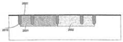
종래의 n채널 JFET의 대표적인 구조가 도 8에 도시되어 있다. JFET는 n형 기판(810)에 형성된다. 이것은 815로 표시된 p웰 영역에 포함된다. JFET의 본체는 소스(832), 채널(838) 및 드레인(834) 영역들을 포함하는 n형 확산 영역인 820으로 도시된다. 게이트 영역(836)은 p형이고, 기판으로의 확산에 의해 형성된다. 소스, 드레인, 및 게이트 영역들에 대한 접촉들은 각각 841, 842 및 840으로 표시된다. JFET의 임계 치수는 855로 표시된 게이트 길이이다. 이것은 최소 접촉 홀 치수(850), 플러스 게이트 영역이 게이트 접촉을 둘러싸는 것을 보증하기 위해 요 구되는 필요한 중첩에 의해 결정된다. 게이트 길이(855)는 850보다 상당히 크다. 이러한 종래의 JFET의 구성의 특징은 이들 소자의 성능을 제한하는데, 이는 채널 길이가 최소 피처 사이즈보다 훨씬 크기 때문이다. 게다가, 드레인 및 소스 영역들에 대한 게이트 확산의 수직 측벽들(861, 862)의 용량들 각각 또한 매우 크다. 게이트-드레인 측벽 용량은 이 분야의 전문가들에게 공지된 용어인 밀러 용량을 형성하며, 높은 주파수에서 소자의 성능을 크게 제한한다.A representative structure of a conventional n-channel JFET is shown in FIG. The JFET is formed on the n-
따라서, 구조가 계속 축소될 때 전술한 문제들을 해결하기 위한 집적 회로 및 소자 구조는 물론, 제조 방법을 갖추는 것이 바람직하다. 옵션으로, 기존 설비 및 장비 기반 구조를 이용하기 위하여 CMOS 소자를 제조하기 위한 방법과 유사한 방법을 이용하여 이러한 새로운 집적 회로 및 소자 구조를 제조하는 것 또한 바람직하다.Therefore, it is desirable to have a fabrication method as well as an integrated circuit and device structure to solve the above-mentioned problems when the structure continues to shrink. Optionally, it is also desirable to fabricate these new integrated circuits and device structures using methods similar to those for manufacturing CMOS devices to take advantage of existing facility and equipment infrastructure.
<발명의 요약>Summary of the Invention
본 발명은 실리콘에서 JFET를 이용하여 상보형 논리 회로를 형성하는 방법을 기술한다. 본 발명은 이상적으로는 디프 서브마이크론 치수, 바람직하게는 65 nm 이하의 치수에 적합하다.The present invention describes a method of forming complementary logic circuits using JFETs in silicon. The present invention is ideally suited for deep submicron dimensions, preferably 65 nm or less.
위의 섹션에서 언급한 바와 같은 현재의 CMOS 및 접합형 전계 효과 트랜지스터 기술의 문제들을 해결하기 위하여, 본 발명은 특히 65 nm 이하의 최소 피처 사이즈에서 이러한 문제들을 해결하기 위한 반도체 소자들의 시스템을 기술한다. 본 발명은 CMOS 소자들에 대해 사용되는 것들과 유사한 반도체 소자들 및 회로들을 형성하기 위한 다수의 방법 및 구조를 기술한다. 이러한 본 발명의 특징은 VLSI 회 로를 설계하고 제조하기 위한 전체 시스템의 상당한 변경 없이 본 발명이 기존의 VLSI 설계 및 제조 흐름에 삽입되는 것을 가능하게 한다. 본 발명의 주요 특성들은 다음과 같다.In order to solve the problems of current CMOS and junction field effect transistor technology as mentioned in the above section, the present invention describes a system of semiconductor devices to solve these problems, especially at the minimum feature size of 65 nm or less. . The present invention describes a number of methods and structures for forming semiconductor devices and circuits similar to those used for CMOS devices. This feature of the present invention enables the present invention to be incorporated into existing VLSI design and manufacturing flows without significant modification of the overall system for designing and manufacturing VLSI circuits. The main features of the present invention are as follows.
1. 본 발명은 회로의 전력 소모의 상당한 감소를 가능하게 한다.1. The present invention enables a significant reduction in the power consumption of the circuit.
2. 본 발명은 게이트 용량의 상당한 감소를 가능하게 한다.2. The present invention enables a significant reduction in gate capacity.
3. 본 발명은 게이트에서의 누설 전류의 상당한 감소를 가능하게 한다.3. The present invention enables a significant reduction of the leakage current at the gate.
4. 본 발명은 소스와 드레인 사이의 누설 전류의 상당한 감소를 가능하게 한다.4. The present invention enables a significant reduction of the leakage current between the source and drain.
5. 본 발명은 VLSI 제조 프로세스의 상당한 간소화를 가능하게 한다.5. The present invention enables significant simplification of the VLSI manufacturing process.
6. 본 발명은 CMOS 기술을 위해 개발된 설계 기반 구조를 이용한다. 종래의 CMOS 셀 라이브러리에서 이용 가능한 모든 복잡한 논리 기능이 본 발명의 소자를 이용하여 구현될 수 있는 것으로 기대된다. 이러한 복잡한 논리 기능들은 인버터, NAND, NOR, 래치, 플립-플롭, 카운터, 멀티플렉서, 인코더, 디코더, 승산기, 산술 논리 유닛, 프로그래머블 셀, 메모리 셀, 마이크로 제어기, JPEG 디코더 및 MPEG 디코더를 포함하지만, 이에 한정되지 않는다.6. The present invention utilizes a design infrastructure developed for CMOS technology. It is expected that all the complex logic functions available in conventional CMOS cell libraries can be implemented using the device of the present invention. These complex logic functions include, but are not limited to, inverters, NAND, NOR, latches, flip-flops, counters, multiplexers, encoders, decoders, multipliers, arithmetic logic units, programmable cells, memory cells, microcontrollers, JPEG decoders, and MPEG decoders. It is not limited.
7. 본 발명은 CMOS에 사용된 기존의 제조 및 테스트 기반구조를 이용한다.7. The present invention utilizes existing fabrication and test infrastructure used in CMOS.
8. 본 발명은 소자의 제조시에 발생하는 결함들을 검출하기 위한 유효 스크린으로서의 전원 누설 전류 측정 방법을 허가한다.8. The present invention permits a method of measuring power leakage current as an effective screen for detecting defects occurring in the manufacture of the device.
본 발명의 기초는 증가 모드로 동작하는 상보형 접합형 전계 효과 트랜지스터(JFET)이다. 이 분야의 전문가들에게 공지되어 있듯이, 증가 모드는 게이트 및 소스 단자들 사이의 전위가 0일 때 트랜지스터가 "오프" 상태에 있는 것을 의미한다. 이 상태에서는, n채널(p채널) JFET의 드레인 단자에 양(음)의 바이어스가 인가될 때 드레인과 소스 사이에는 거의 또는 전혀 전류 흐름이 존재하지 않는다. 게이트의 전위가 증가(감소)함에 따라, n채널(p채널) JFET는 고전도 체제에 들어간다. 이 모드에서, 드레인에 양(음)의 바이어스 인가시 드레인과 소스 사이에는 한정된 전류가 흐른다. 종래의 증가 모드 JFET 소자들의 한계는 이들의 전류 구동이 일 다이오드 드롭보다 작은 최대 게이트 전압에 의해 제한된다는 점이다. 일 다이오드 드롭(내부 전위)을 초과하는 게이트 전압은 게이트-채널 다이오드를 턴온시키는데, 이는 JFET의 바람직하지 않은 동작 모드이다. 이러한 한계는 본 발명에서 바이어싱 전압 VDD를 일 다이오드 드롭보다 작게 제한함으로써 해결된다. JFET의 낮은 전류 구동의 문제는 JFET의 채널 길이를 100 nm 이하의 치수로 축소함으로써 해결된다. JFET 게이트 길이가 70 nm보다 작고, 전원 전압이 0.5V일 때, 상보형 JFET 소자의 전류 출력 및 상보형 JFET 소자들로 이루어진 인버터의 스위칭 속도는 종래의 CMOS 소자에 양호하게 필적한다.The basis of the present invention is a complementary junction type field effect transistor (JFET) operating in increasing mode. As is known to those skilled in the art, an incremental mode means that the transistor is in an "off" state when the potential between the gate and source terminals is zero. In this state, there is little or no current flow between the drain and the source when a positive bias is applied to the drain terminal of the n-channel (p-channel) JFET. As the potential of the gate increases (decreases), the n-channel (p-channel) JFET enters a high conductivity regime. In this mode, a limited current flows between the drain and the source when a positive (negative) bias is applied to the drain. A limitation of conventional incremental mode JFET devices is that their current drive is limited by the maximum gate voltage less than one diode drop. The gate voltage above one diode drop (internal potential) turns on the gate-channel diode, which is an undesirable mode of operation of the JFET. This limitation is solved in the present invention by limiting the biasing voltage VDD to less than one diode drop. The problem of low current driving of the JFET is solved by reducing the channel length of the JFET to dimensions below 100 nm. When the JFET gate length is less than 70 nm and the power supply voltage is 0.5V, the current output of the complementary JFET device and the switching speed of the inverter composed of the complementary JFET devices are comparable to conventional CMOS devices.
JFET의 속도-전력 성능이 70 nm 이하의 치수에서 CMOS 소자에 필적하지만, JFET의 최대 전원 전압은 여전히 일 다이오드 드롭 이하로 제한된다는 점에 유의해야 한다. 보다 높은 전압 레벨로 구동되는 외부 회로에 대한 인터페이스를 필요로 하는 소정의 응용들을 만족시키기 위하여, 본 발명은 CMOS 소자들을 또한 형성하기 위한 구조들 및 방법들을 포함한다. 본 발명에서 기술되는 CMOS 소자들은 다음과 같은 점에서 종래의 CMOS와 다르다.It should be noted that while the JFET's speed-power performance is comparable to CMOS devices in dimensions below 70 nm, the JFET's maximum supply voltage is still limited to less than one diode drop. In order to satisfy certain applications that require an interface to an external circuit driven at a higher voltage level, the present invention includes structures and methods for forming CMOS devices as well. The CMOS devices described in the present invention differ from the conventional CMOS in the following points.
1. CMOS가 상보형 JFET들과 집적된다.1. CMOS is integrated with complementary JFETs.
2. 본 발명의 일 실시예에서, CMOS는 "스페이서" 없이 형성된다.2. In one embodiment of the invention, the CMOS is formed without a "spacer".
3. 본 발명의 상기 실시예에서, CMOS 단자에 대한 접촉들은 평면 또는 동일 레벨인데, 이는 소자들의 제조성을 향상시킨다.3. In the above embodiment of the present invention, the contacts to the CMOS terminals are flat or at the same level, which improves the manufacturability of the devices.
4. 이러한 CMOS 소자의 다른 현저한 특징들은 전술하였다.4. Other salient features of this CMOS device have been described above.
전술한 본 발명의 특징들, 이점들 및 목적들이 달성되는 방식이 상세히 이해될 수 있도록, 위에 간략히 요약된 본 발명에 대한 보다 구체적인 설명이 첨부된 도면들에 도시되는 발명의 실시예들을 참조하여 이루어질 수 있다.BRIEF DESCRIPTION OF THE DRAWINGS In order that the features, advantages, and objects of the invention described above can be understood in detail, a more detailed description of the invention briefly summarized above is made with reference to the embodiments of the invention shown in the accompanying drawings. Can be.
그러나, 첨부된 도면들은 본 발명의 전형적인 실시예들을 나타낼 뿐이며, 따라서 본 발명은 다른 동일하게 유효한 실시예들을 허용할 수 있으므로, 본 발명의 범위를 한정하는 것으로 간주되어서는 안 된다는 점에 유의해야 한다.It should be noted, however, that the appended drawings illustrate only typical embodiments of the invention and, therefore, the invention may permit other equally effective embodiments and therefore should not be considered as limiting the scope of the invention. .
도 1은 상보형 JFET 인버터를 나타내는 도면.1 shows a complementary JFET inverter.
도 2a는 웰이 소스에 결합된 상보형 JFET 인버터의 도면.2A is a diagram of a complementary JFET inverter with wells coupled to a source.
도 2b는 웰이 게이트에 결합된 상보형 JFET 인버터의 도면.2B is a diagram of a complementary JFET inverter with wells coupled to gates.
도 2c는 웰이 외부 패드에 결합된 상보형 JFET 인버터의 도면.2C shows a complementary JFET inverter with wells coupled to an external pad.
도 3a는 JFET의 레이아웃의 도면.3A is a diagram of a layout of a JFET.
도 3b는 도 3a에 대응하는 폴리 게이트 JFET의 단면도.3B is a cross-sectional view of the poly gate JFET corresponding to FIG. 3A.
도 3c는 게이트 및 채널을 통해 JFET의 도핑 프로파일을 나타내는 그래프.3C is a graph showing the doping profile of a JFET through gates and channels.
도 4는 종래의 MOSFET와 유사한 폴리 게이트 JFET의 단면도.4 is a cross-sectional view of a poly gate JFET similar to a conventional MOSFET.
도 5는 모든 접촉이 폴리실리콘을 통해 형성된 폴리 게이트 평면 JFET의 단면도.5 is a cross-sectional view of a poly gate planar JFET with all contacts formed through polysilicon.
도 6은 채널 영역이 에피텍셜 성장된 폴리 게이트 평면 JFET의 단면도.6 is a cross-sectional view of a poly gate planar JFET with epitaxially grown channel regions.
도 7은 채널 영역이 에피텍셜 성장되고 다결정 반도체 합금 게이트가 탄소, 실리콘 및 게르마늄을 포함하는 폴리 게이트 평면 JFET의 단면도.7 is a cross-sectional view of a poly gate planar JFET in which the channel region is epitaxially grown and the polycrystalline semiconductor alloy gate comprises carbon, silicon, and germanium.
도 8은 종래의 n채널 JFET의 단면도.8 is a cross-sectional view of a conventional n-channel JFET.
도 9는 도 5에 도시된 바와 같은 상보형 JFET 구조를 형성하는 흐름도. 흐름도의 각각의 단계는 도 10-20에서 더 설명된다.9 is a flow chart of forming a complementary JFET structure as shown in FIG. Each step of the flowchart is further described in FIGS. 10-20.
도 10은 분리 영역의 형성 후의 실리콘 웨이퍼의 단면도.10 is a sectional view of a silicon wafer after formation of the isolation region.
도 11은 n웰 및 p웰의 형성 후의 실리콘 웨이퍼의 단면도.11 is a cross-sectional view of a silicon wafer after formation of n wells and p wells.
도 12a는 nJFET의 채널 영역의 형성 후의 실리콘 웨이퍼의 단면도.12A is a sectional view of a silicon wafer after formation of a channel region of an nJFET.
도 12b는 pJFET의 채널 영역의 형성 후의 실리콘 웨이퍼의 단면도.12B is a cross-sectional view of the silicon wafer after formation of the channel region of the pJFET.
도 13은 폴리실리콘 피착 및 폴리실리콘의 선택적 도핑 후의 실리콘 웨이퍼의 단면도.13 is a cross-sectional view of a silicon wafer after polysilicon deposition and selective doping of polysilicon.
도 14는 폴리실리콘 층 상의 보호 코팅 피착 후의 실리콘 웨이퍼의 단면도.14 is a cross-sectional view of a silicon wafer after deposition of a protective coating on a polysilicon layer.
도 15는 포토리소그라피 및 에칭에 의한 폴리실리콘 정의 후의 실리콘 웨이퍼의 단면도.15 is a cross-sectional view of a silicon wafer after polysilicon definition by photolithography and etching.
도 16a는 p채널 JFET의 게이트와 드레인/소스 간의 링크 영역 도핑 후의 실리콘 웨이퍼의 단면도.16A is a cross-sectional view of a silicon wafer after doping the link region between the gate and drain / source of the p-channel JFET.
도 16b는 n채널 JFET의 게이트와 드레인/소스 간의 링크 영역의 도핑 후의 실리콘 웨이퍼의 단면도.Fig. 16B is a cross sectional view of the silicon wafer after doping of the link region between the gate and drain / source of the n-channel JFET.
도 17은 폴리실리콘 구조들 간의 빈 공간을 채운 다음 평탄화를 수행한 후의 실리콘 웨이퍼의 단면도.FIG. 17 is a cross-sectional view of a silicon wafer after filling the void spaces between polysilicon structures followed by planarization. FIG.
도 18은 노출된 폴리실리콘 표면 상의 자기 정렬 실리사이드의 형성 후의 실리콘 웨이퍼의 단면도.18 is a cross-sectional view of a silicon wafer after formation of self-aligned silicide on the exposed polysilicon surface.
도 19는 폴리실리콘 상의 유전체 층 피착 및 접촉 홀들의 후속 에칭 후의 실리콘 웨이퍼의 단면도.19 is a cross-sectional view of a silicon wafer after dielectric layer deposition on polysilicon and subsequent etching of contact holes.
도 20은 금속 피착 및 정의 후의 실리콘 웨이퍼의 단면도.20 is a cross-sectional view of a silicon wafer after metal deposition and definition.
도 21-24는 도 9로부터 적합화된 프로세스를 이용하는 MOS 트랜지스터의 형성을 나타내는 도면.21-24 illustrate formation of a MOS transistor using the process adapted from FIG.
도 21은 분리 영역, 웰 구조, 임계치 주입 및 게이트 유전체의 형성 후의 실리콘 웨이퍼의 단면도. 게이트 유전체가 성장되며, MOS 게이트 영역을 둘러싸는 영역들을 제외하고 웨이퍼로부터 에칭된다.21 is a cross-sectional view of a silicon wafer after formation of isolation regions, well structures, threshold implants and gate dielectrics. The gate dielectric is grown and etched from the wafer except for the regions surrounding the MOS gate region.
도 22는 폴리실리콘 피착, 폴리실리콘 도핑 및 폴리실리콘 상부의 보호층의 형성 후의 실리콘 웨이퍼의 단면도.FIG. 22 is a cross-sectional view of a silicon wafer after polysilicon deposition, polysilicon doping, and formation of a protective layer overlying polysilicon; FIG.
도 23은 폴리실리콘 정의 후의 실리콘 웨이퍼의 단면도.23 is a cross-sectional view of a silicon wafer after polysilicon definition.
도 24는 링크 영역이 이온 주입에 의해 게이트와 소스/드레인 사이에 형성된 후의 실리콘 웨이퍼의 단면도.Fig. 24 is a sectional view of the silicon wafer after the link region is formed between the gate and the source / drain by ion implantation.
도 25는 동일 웨이퍼 상에 JFET 및 MOSFET를 형성하기 위한 완전한 흐름도. 각각의 단계는 도 26-30에서 더 설명된다.25 is a complete flow chart for forming a JFET and a MOSFET on the same wafer. Each step is further described in FIGS. 26-30.
도 26은 n웰 및 p웰이 형성된 후의 실리콘 웨이퍼의 단면도.Fig. 26 is a sectional view of a silicon wafer after n wells and p wells are formed.
도 27은 JFET의 채널이 형성된 후의 실리콘 웨이퍼의 단면도.Fig. 27 is a sectional view of the silicon wafer after the channel of the JFET is formed.
도 28은 MOS 채널이 형성된 후의 실리콘 웨이퍼의 단면도.Fig. 28 is a sectional view of the silicon wafer after the MOS channel is formed.
도 29는 MOS 및 JFET의 소스 및 드레인 영역이 형성된 후의 실리콘 웨이퍼의 단면도.Fig. 29 is a sectional view of the silicon wafer after the source and drain regions of the MOS and JFETs are formed.
도 30a는 접촉 홀들 및 금속 접속들이 형성된 후의 실리콘 웨이퍼의 단면도.30A is a cross-sectional view of the silicon wafer after contact holes and metal connections are formed.
도 30b는 접촉 홀들 및 금속 접속들이 형성된 후의 NMOS 및 nJFET의 레이아웃을 나타내는 도면.30B illustrates the layout of an NMOS and nJFET after contact holes and metal connections are formed.
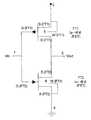
본 발명을 이용하여 형성된 인버터의 회로도가 도 1에 도시되어 있다. 온 및 오프 조건 하에서의 2개의 트랜지스터의 동작 단자 전압들이 테이블 1에 나타나 있다.A circuit diagram of an inverter formed using the present invention is shown in FIG. The operating terminal voltages of the two transistors under on and off conditions are shown in Table 1.
[표 1] 온 및 오프 조건 하에서의 CFET 게이트의 단자 전압들Table 1 Terminal Voltages on CFET Gate Under On and Off Conditions

도 1에 도시된 회로의 동작은 대응하는 CMOS 회로의 동작과 매우 유사하다. JFET는 본 발명에서 종래의 CMOS 기술의 전압 레벨과 유사한 전압 레벨로 동작한다. 입력 전압은 0과 Vdd 사이에서 변한다. 출력 전압은 입력 전압과 반대로 Vdd와 0 사이에서 변한다. 따라서, 인버터의 두 상태에 대해, 입력 단자에 인가되는 전압이 0과 Vdd일 때, 출력 전압은 각각 Vdd와 0이 된다. 이것은 위의 표 1에 나타난 바와 같이 온 및 오프로 스위칭되는 2개의 트랜지스터(FT1, FT2)에 의해 달성된다.The operation of the circuit shown in FIG. 1 is very similar to that of the corresponding CMOS circuit. The JFET operates at a voltage level similar to that of conventional CMOS technology in the present invention. The input voltage varies between 0 and Vdd. The output voltage varies between Vdd and 0 as opposed to the input voltage. Thus, for both states of the inverter, when the voltages applied to the input terminals are 0 and Vdd, the output voltages become Vdd and 0, respectively. This is accomplished by two transistors FT1 and FT2 that are switched on and off as shown in Table 1 above.
이 분야의 전문가들에게 공지되어 있듯이, JFET는 소스와 드레인 사이의 채널의 전도 특성을 제어하는 제어 신호를 게이트에 인가함으로써 동작한다. 게이트는 채널과 함께 p-n 접합을 형성한다. 소스에 대한 게이트의 전압은 게이트-채널 접합의 공핍 영역의 폭을 제어한다. 채널의 공핍되지 않은 부분은 전도에 이용될 수 있다. 따라서, 채널은 JFET 트랜지스터의 게이트 및 소스 단자들에 적절한 전압을 인가함으로써 턴온 및 턴오프된다. 채널이 턴온되고, 드레인에 적절한 전압이 인가될 때 소스와 드레인 사이에 전류가 흐를 것이다.As is known to those skilled in the art, the JFET operates by applying a control signal to the gate that controls the conduction characteristics of the channel between the source and the drain. The gate forms a p-n junction with the channel. The voltage at the gate to the source controls the width of the depletion region of the gate-channel junction. Undepleted portions of the channel can be used for conduction. Thus, the channel is turned on and off by applying an appropriate voltage to the gate and source terminals of the JFET transistor. The current will flow between the source and the drain when the channel is turned on and an appropriate voltage is applied to the drain.
JFET 인버터 내의 JFET 트랜지스터들(FT1, FT2)은 CMOS 인버터 내의 MOS 트랜지스터들과 매우 유사한 방식으로 기능한다. CMOS 인버터의 동작은 이 분야의 전문가들에게 공지되어 있다. p채널 JFET(FT1)는 그의 소스 단자에서 전원에 접속된다. n채널 JFET(FT2)는 그의 소스 단자에서 접지에 접속된다. 2개의 트랜지스터의 드레인 단자들은 함께 그리고 게이트의 출력 단자에 접속된다. 도 1에 도시된 바와 같이, p채널 JFET(FT1)의 게이트 및 n채널 JFET(FT2)의 게이트는 함께, 그리고 게이트의 입력 단자에 접속된다. 본 명세서의 나머지 부분에서 이러한 회로 구성을 CFET 인버터라고 한다. 일반적으로, p채널 및 n채널 JFET와 유사한 방식으로 형성된 게이트를 CFET 게이트라 한다.The JFET transistors FT1 and FT2 in the JFET inverter function in a very similar way to the MOS transistors in the CMOS inverter. The operation of CMOS inverters is known to those skilled in the art. The p-channel JFET FT1 is connected to a power supply at its source terminal. The n-channel JFET FT2 is connected to ground at its source terminal. The drain terminals of the two transistors are connected together and to the output terminal of the gate. As shown in Fig. 1, the gate of the p-channel JFET FT1 and the gate of the n-channel JFET FT2 are connected together and to the input terminal of the gate. In the remainder of this specification, this circuit configuration is referred to as a CFET inverter. In general, gates formed in a manner similar to p-channel and n-channel JFETs are referred to as CFET gates.
본 명세서에서 본 발명의 완전한 구현을 보이기 위하여 인버터의 기능이 더 상세히 설명된다. 이것은 먼저 표 2에 나타낸 트랜지스터의 소스 및 드레인 단자들의 전압을 설명함으로써 달성된다. 예시적이고 비제한적인 설명에서, 전원 전압은 0.5V로 고정된다.The function of the inverter is described in more detail herein to show a complete implementation of the invention. This is accomplished by first describing the voltages of the source and drain terminals of the transistors shown in Table 2. In the illustrative and non-limiting description, the power supply voltage is fixed at 0.5V.
[표 2] CFET 게이트 내의 JFET의 접합 전압[Table 2] Junction Voltage of JFET in CFET Gate

p채널 JFET의 게이트는 n형 실리콘으로 형성되고, 채널은 p형으로 도핑된다. p채널 JFET의 도핑 프로파일은 게이트 단자 상의 전압이 소스 단자에 대해 0 볼트일 때 채널을 통한 전도를 턴오프하도록 설계된다. 이러한 소자는 증가 모드 소자이다. p채널 JFET의 이러한 특성은 게이트(p형)와 채널(n형) 간의 p-n 접합에서의 내부 전위 때문이다. FT1의 소스가 0.5V의 VDD에 결합되므로, FT1의 게이트가 또한 0.5V에 있을 때, n형 채널과 p형 게이트 간의 외부 바이어스는 0.0V가 된다. 이것은 오프 조건의 FT1을 나타낸다. p채널 트랜지스터의 게이트에서의 바이어스가 0.0V로 감소함에 따라, 게이트와 소스 단자들 간의 음 전압은 -0.5V로 변하며, 이는 공핍층을 제거하여 소스에서 드레인으로 전류가 흐르게 한다. 이것은 온 조건의 FT1을 나타낸다.The gate of the p-channel JFET is formed of n-type silicon and the channel is doped to p-type. The doping profile of the p-channel JFET is designed to turn off conduction through the channel when the voltage on the gate terminal is 0 volts relative to the source terminal. Such devices are incremental mode devices. This characteristic of the p-channel JFET is due to the internal potential at the p-n junction between the gate (p-type) and the channel (n-type). Since the source of FT1 is coupled to VDD of 0.5V, the external bias between the n-type channel and the p-type gate becomes 0.0V when the gate of FT1 is also at 0.5V. This represents FT1 in the off condition. As the bias at the gate of the p-channel transistor decreases to 0.0V, the negative voltage between the gate and source terminals changes to -0.5V, which removes the depletion layer and allows current to flow from the source to the drain. This represents FT1 in on condition.
본 발명의 중요한 가르침은 FT1이 온 조건에 있을 때 게이트 전류를 어떻게 제한하는가이다. 이 조건 하에서 채널-게이트 다이오드는 0.5V로 순방향 바이어스되며, 따라서 트랜지스터의 게이트를 통해 흐르는 한정된 누설 전류가 존재한다. 이를 게이트 누설이라 한다. 게이트 누설의 크기는 게이트-채널 접합 양단의 내부 전위에 의해 제어된다. 이러한 CFET 인버터가 실리콘 기반 회로들에 대해 0.5V 이하의 전원 전압(VDD)으로 동작할 때, 내부 전위는 게이트 누설 전류를 매우 작은 양으로 제한한다. 따라서, CFET 인버터는 설계 및 동작 특성 양면에서 CMOS 인버터와 유사한 방식으로 동작한다. 전원 전압에 대한 제한은 내부 전위의 차이로 인해 다른 재료들에 대해 다를 수 있다. 마찬가지로, n채널 JFET에 대한 바이어스 전압은 반대로 되어, 트랜지스터는 게이트-소스 바이어스가 0으로 감소될 때 "턴오프"되고, 게이트-소스 바이어스가 게이트 전류를 제한하기 위해 0.5V로 제한되는 전원 전압(VDD)과 동일할 때 턴온된다. 전형적인 게이트-채널 접합의 게이트 전류는 1μA/cm2 내지 100 mA/cm2의 범위로 설계된다. 이와 달리, 45 나노미터 리소그라피 및 적절히 축소된 게이트 유전체 두께로 형성된 MOS 트랜지스터에 대해, 게이트 전류는 1000 A/cm2를 초과하도록 설계된다.An important teaching of the present invention is how to limit the gate current when FT1 is in the on condition. Under this condition, the channel-gate diode is forward biased to 0.5V, so there is a finite leakage current flowing through the gate of the transistor. This is called gate leakage. The magnitude of the gate leakage is controlled by the internal potential across the gate-channel junction. When this CFET inverter operates with a supply voltage (VDD) of less than 0.5V for silicon based circuits, the internal potential limits the gate leakage current to a very small amount. Thus, CFET inverters operate in a manner similar to CMOS inverters in both design and operating characteristics. Limits on power supply voltage may differ for other materials due to differences in internal potentials. Similarly, the bias voltage for the n-channel JFET is reversed, so that the transistor is " turned off " when the gate-source bias is reduced to zero, and the supply voltage (which is limited to 0.5V to limit the gate current). Is turned on when equal to VDD). The gate current of a typical gate-channel junction is designed in the range of1 μA / cm2 to 100 mA / cm2 . In contrast, for MOS transistors formed with 45 nanometer lithography and properly scaled gate dielectric thickness, the gate current is designed to exceed 1000 A / cm2 .
JFET 트랜지스터의 입력 용량은 게이트-채널 단자들에 의해 형성되는 다이오드의 접합 용량이다. 이 다이오드의 용량은 10-8F/cm2 내지 10-6 F/cm2의 범위 내이며, 100 Å 내지 3000 Å의 범위 내인 접합의 공핍층 폭의 두께에 의해 결정된다. 45 나노미터 설계 규칙 및 10 Å 두께의 산화물로 형성된 MOS 트랜지스터의 입력 용량은 JFET의 대응 입력 용량보다 높은 크기 수준이다. 이러한 특징은 저전력 동작 관점에서 JFET를 매우 매력적이게 한다.The input capacitance of the JFET transistor is the junction capacitance of the diode formed by the gate-channel terminals. The capacity of this diode is in the range of 10−8 F / cm2 to 10−6 F / cm2 , and is determined by the thickness of the depletion layer width of the junction in the range of 100 kV to 3000 kV. The input capacitance of MOS transistors formed from 45 nanometer design rules and 10 Å thick oxide is on the order of magnitude higher than the JFET's corresponding input capacitance. This feature makes JFETs very attractive from a low power operating point of view.
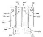
JFET 트랜지스터는 또한 제4 전기 단자, 즉 웰을 갖는다. 본 발명의 일 실시예는 도 2a에 도시된 바와 같이 양 JFET들에 대해 웰이 소스 단자에 접속되는 것으로 설명된다.The JFET transistor also has a fourth electrical terminal, ie a well. One embodiment of the present invention is described as the well is connected to the source terminal for both JFETs as shown in FIG. 2A.
도 2b는 웰이 게이트에 결합되고, 상부 및 하부 양자로부터 채널의 전도도를 조절하는 데 사용되는 본 발명의 다른 실시예를 나타낸다.2B shows another embodiment of the present invention in which a well is coupled to the gate and used to adjust the conductivity of the channel from both top and bottom.
도 2c는 n채널 JFET의 웰이 JFET에 임의의 신호를 인가하는 데 사용될 수 있는 외부 단자에 접속되는 본 발명의 또 다른 실시예를 나타낸다. 본 발명의 또 다른 실시예에서, n채널 JFET의 웰은 부동 상태로 남겨진다. 대응하는 설명은 p채널 JFET에도 적용된다. 소자의 제조시에 발생하는 결함들을 검출하기 위한 유효 스크린으로서 전원 누설 전류를 측정하는 것이 이 분야의 전문가들에게 공지되어 있다. 이 방법은 때때로 이 분야의 전문가들에 의해 Iddq 테스트로서 지칭된다. 이 방법은 350 nm 이상의 최소 선폭을 갖는 CMOS에 효과적이다. 350 nm 이하의 최소 선폭으로의 CMOS 축소는 고유 누설 전류를 결함 유도 누설 전류에 필적하는 레벨로 증가시켜, Iddq 테스트를 효과 없게 한다. 100 nm 이하의 최소 선폭을 갖는 MOS 소자들에 대해, 고유 누설 전류를 제거하기 위해 MOS 소자의 웰 전압을 바이어스하는 것은 게이트 누설, 접합 터널링 누설 등과 같은 새로운 누설 요소들을 발생시킨다. 본 발명에서, JFET의 웰 전압을 바이어싱하는 것은 고유 누설 전류를 피코 암페어 범위로 효과적으로 줄일 수 있다. 이것은 Iddq 테스트를, 100 nm 이하의 최소 선폭을 갖는 소자들의 제조시에 발생하는 결함들을 검출하기 위한 유효 스크린이 되게 한다.FIG. 2C illustrates another embodiment of the present invention in which the well of an n-channel JFET is connected to an external terminal that can be used to apply any signal to the JFET. In another embodiment of the present invention, the wells of the n-channel JFET are left floating. The corresponding description also applies to p-channel JFETs. It is known to those skilled in the art to measure the power leakage current as an effective screen for detecting defects occurring in the manufacture of the device. This method is sometimes referred to by experts in the art as the Iddq test. This method is effective for CMOS having a minimum line width of 350 nm or more. CMOS shrinkage to a minimum line width of less than 350 nm increases the intrinsic leakage current to a level comparable to the fault induced leakage current, making the Iddq test ineffective. For MOS devices with a minimum line width of less than 100 nm, biasing the well voltage of the MOS device to remove inherent leakage currents creates new leakage elements such as gate leakage, junction tunneling leakage, and the like. In the present invention, biasing the well voltage of the JFET can effectively reduce the inherent leakage current to the pico amp range. This makes the Iddq test an effective screen for detecting defects that occur in the manufacture of devices with a minimum line width of less than 100 nm.
도 3a는 이러한 회로 구조를 형성하는 데 사용되는 JFET 트랜지스터의 예시적이고 비제한적인 레이아웃을 나타낸다. n채널 JFET의 소스, 드레인, 게이트 및 웰 탭은 각각 330, 340, 375 및 368로 주어진다. 이들 단자에 대한 접촉들은 각각 372, 374, 373 및 371로 표시된다.3A shows an exemplary, non-limiting layout of the JFET transistors used to form this circuit structure. The source, drain, gate and well taps of the n-channel JFET are given as 330, 340, 375 and 368, respectively. Contacts for these terminals are indicated by 372, 374, 373 and 371, respectively.
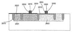
도 3b는 4개의 단자, 즉 소스(330), 게이트(370), 드레인(340) 및 p웰(310)로 구성되는 n채널 JFET의 구조의 단면도를 나타낸다. JFET는 315로 표시된 실리콘의 영역에 형성된다. JFET는 320으로 표시된 영역들에 의해 주변 반도체로부터 분리되는데, 이들 영역은 실리콘 이산화물과 같은 절연 재료로 채워진다. 소스와 드레인 사이의 채널은 물체 350으로 도시된다. n채널 JFET에 대해, 소스 및 드레인은 인, 비소 또는 안티몬과 같은 도너 타입의 불순물로 실리콘을 도핑함으로써 형성되는 고농도 도핑된 n형 영역들이다. 웰은 붕소 또는 인듐과 같은 억셉터 불순물로 도핑된다. 채널은 소스와 드레인을 접속하는 n형으로 도핑된 좁은 영역이다. 게이트는 고농도로 p+ 도핑된 폴리실리콘 영역(375)으로부터의 도펀트들의 확산과 같은 방법들에 의해 채널 내에 형성된 얕은 p형 영역(370)이다.3B shows a cross-sectional view of the structure of an n-channel JFET consisting of four terminals,
게이트(370) 및 채널(350)을 통한 실리콘 표면으로부터의 다양한 깊이에서의 도핑 프로파일이 도 3c에 도시되어 있다. 곡선 381은 실리콘 표면에서 시작하는 게이트 영역의 예시적인 도핑 프로파일이다. 곡선 382, 383 및 384는 채널, 웰 및 벌크 영역들의 도핑 프로파일을 나타낸다. n형 JFET에 대하여, 381은 p형 게이트 영역의 도핑 프로파일이고, 382는 n형 채널 영역의 프로파일이고, 383은 p형 웰 영역의 프로파일이고, 384는 주변 n형 벌크 영역의 프로파일이다. 게이트-채널 접합은 385로 주어지고, 채널-웰 접합은 386으로 주어지고, 웰-벌크 영역 접합은 387로 주어진다. 실리콘의 표면으로부터의 게이트와 채널 간의 접합의 깊이(385)는 채널과 p웰 간의 접합의 깊이(386)보다 작다.Doping profiles at various depths from the silicon surface through
본 발명은 또한 이온 주입과 같이 p형 게이트 접합을 형성하기 위한 다른 방법들을 가르친다. 본 발명은 또한 이 분야의 전문가들에게 공지된 바와 같은 플라즈마 이멀션 주입과 같이 게이트를 도핑하는 다른 방법들을 커버한다.The present invention also teaches other methods for forming a p-type gate junction, such as ion implantation. The invention also covers other methods of doping the gate, such as plasma emulsion injection as known to those skilled in the art.
도 3b에서, 영역 375는 고농도로 p형 도핑된 폴리실리콘의 슬랩이며, 게이트(370)의 도핑을 위한 소스로서 작용한다. p형 게이트는 소스와 드레인 간의 채널 양단의 전도를 제어하는 데 사용된다. 이러한 신규한 제조 기술에 의해, 게이트는 게이트와 저항 접촉을 또한 형성하는 고농도로 도핑된 폴리실리콘으로부터 채널 영역 내에 확산된다. 이것은 폴리실리콘이 게이트를 외부 회로에 접속시키는 데 사용될 수 있게 한다.In FIG. 3B,
웰에 대한 저항 접촉은 물체 368로 표시된 웰 탭에 의해 이루어진다. JFET의 네 단자, 즉 웰, 소스, 게이트 및 드레인에 대한 접촉들은 도 3b에서 물체들 371, 372, 373 및 374로 각각 도시되어 있다. p웰 탭(368) 아래의 영역은 양호한 저항 접촉을 형성하기 위하여 p형 불순물로 고농도로 도핑된다. p웰(310)은 JFET의 p웰이 분리되어야 하는 응용들을 위해 315로 표시된 n웰에 형성된다. p웰이 접지 전위에 접속되는 응용들에 대해, n웰은 필요 없게 된다. 본 발명은 이러한 사례들 양자를 커버한다.Resistive contact to the well is made by a well tap, represented by
도핑 타입들은 도 3b 및 3c에 설명된 것들과 관련하여 p채널 JFET에 대해 반대로 되며, 즉 p형 영역들은 n형 영역들로 대체되고, n형 영역들은 p형 영역들로 대체된다. 폴리실리콘(375)으로 JFET의 게이트를 도핑하는 본 발명의 신규성은 p채널 JFET에 대해서도 유지됨에 유의해야 한다.Doping types are reversed for p-channel JFETs with respect to those described in FIGS. 3b and 3c, ie p-type regions are replaced with n-type regions and n-type regions are replaced with p-type regions. It should be noted that the novelty of the invention of doping the gate of the JFET with
JFET의 다른 실시예가 도 4에 도시되어 있다. 이 도면은 MOS 트랜지스터와 매우 유사한 n채널 JFET의 단면도를 나타낸다. n채널 JFET의 구조가 여기서 설명된다. 이 구조는 또한 위의 단락에서 설명된 바와 같이 적절한 도핑 변경으로 p채널 JFET에 대해 되풀이될 것임은 당연하다. JFET는 물체 400으로 도시되어 있다. JFET가 형성된 p웰은 물체 310으로 표시된다. JFET에 대한 분리는 실리콘 이산화물 또는 다른 적절한 재료와 같은 절연 재료로 채워진 영역(320)에 의해 제공된다. 이 구조는 도 3에 도시된 대응 구조와 유사하다. 고농도로 도핑된 n형 영역들은 소스 및 드레인 영역을 형성하고, 각각 420 및 430으로 표시된다. 소스와 드레인 사이의 채널 영역은 n형으로 저농도 도핑되고 450으로 표시된다. 게이트 영역은 p형으로 도핑되고 440으로 표시된다. 이 영역은 460으로 표시된 고농도 p형 도핑된 폴리실리콘으로부터 확산된다. 실리콘 이산화물 및 질화물 층들의 조합으로 구성된 465로 표시된 절연 영역이 여기에 삽입되어 게이트를 둘러싼다. 본 명세서에서 이 물체를 "스페이서"라고 한다. 본 발명의 일 실시예에서, 영역들(420, 430, 460, 368)의 상부면들은 462로 표시된 실리사이드라고 하는 금속 화합물들 중 하나로 된 고전도층으로 커버된다. 실리사이드 층은 웰 탭, 소스, 드레인 및 게이트 영역에 자기 정렬되며, 이는 실리사이드가 실리콘 또는 폴리실리콘이 노출된 영역에만 형성됨을 의미한다. 스페이서의 주요 목적은 자기 정렬 실리사이드가 형성될 때 소스 및 드레인 영역을 게이트 영역으로부터 분리하는 것이다. 이것은 또한 소자 내의 접촉으로부터 전류의 효율적인 분배를 가능하게 한다. 웰 탭, 소스, 드레인 및 게이트 영역에 대한 접촉들은 도 3에서와 유사한 방식으로 행해지며, 각각 371, 372, 373 및 374로 표시된다.Another embodiment of a JFET is shown in FIG. 4. This figure shows a cross-sectional view of an n-channel JFET that is very similar to a MOS transistor. The structure of an n-channel JFET is described here. It is natural that this structure will also be repeated for p-channel JFETs with appropriate doping changes as described in the paragraph above. JFET is shown as object 400. The p well in which the JFET is formed is represented by
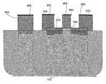
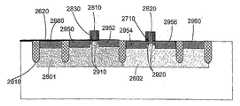
도 5에 도시된 바와 같이, JFET의 다른 실시예에서, JFET의 모든 단자, 즉 소스, 게이트, 드레인 및 웰에 대한 접촉들은 모두 폴리실리콘으로 형성된다. 이 구조는 모든 단자에 대한 접촉들이 동일 레벨을 갖는 바람직한 특성을 갖는다. n채널 JFET는 310으로 표시된 p웰에 형성되는데, 이는 절연 영역(320)에 의해 모든 측부로부터 분리된다. 이 구조는 도 3에 도시된 대응 구조와 유사하다. JFET의 소스는 고농도 n형 도핑된 영역들(520, 522)의 조합에 의해 형성된다. JFET의 드레인 또한 고농도 도핑된 n형 영역들(524, 526)의 조합에 의해 형성된다. 채널(550)은 드레인과 소스 사이의 얕은 n형 도핑 영역이다. 실리콘 내에 확산된 p형 게이트 영역은 540으로 표시된다. 블록들(530, 532)은 고농도 n형 폴리실리콘 도핑 영역들이다. 영역(520)은 폴리실리콘으로부터 실리콘으로 n형 불순물을 확산시킴으로써 형성된다. 마찬가지로, 영역(524)은 폴리실리콘 영역(532)으로부터 실리콘으로 n형 불순물을 확산시킴으로써 형성된다. 게이트 영역(540)은 p형 폴리실리콘(560)으로부터 실리콘으로의 p형 불순물 확산에 의해 형성된다. 영역들(522, 526)은 소스 및 드레인 영역(520, 524)을 각각 채널(550)에 접속한다. 530, 532 및 560으로 표시된 폴리실리콘 영역들은 각각 영역들(520, 524, 540)과 저항 접촉한다. 영역들(522, 526)은 이온 주입, 플라즈마 이멀션 주입, 또는 다른 유사한 도핑 방법들과 같은 외부 도핑에 의해 형성된다. 웰 탭은 고농도 p형 도핑 폴리실리콘(562)과 p형 영역(368) 사이의 저항 접촉에 형성된다. 트랜지스터에 대한 접촉들은 물체들 530, 532, 560 및 562의 상부에 형성된다. 이러한 영역들의 저항 접촉 저항을 줄이기 위하여, 580으로 표시된 자기 정렬 실리사이드가 폴리실리콘 층의 상부에 형성된다. 본 발명의 다른 실시예에서, 트랜지스터의 단자들에 대한 접촉들은 폴리실리콘에 대해 직접 이루어진다.As shown in FIG. 5, in another embodiment of the JFET, all the terminals of the JFET, that is, the contacts to the source, gate, drain, and well, are all formed of polysilicon. This structure has the desirable property that the contacts to all terminals have the same level. An n-channel JFET is formed in the p well, denoted 310, which is separated from all sides by
본 발명의 다른 실시예에서, 실리콘 기판의 상부면은 도 6에 도시된 채널 및 게이트를 형성하도록 적절히 도핑된 실리콘-게르마늄 합금의 에피텍셜 피착에 의해 형성된다. 이 구조는 절연 영역들(320)을 가진 웰(310)에 형성된다. 본 실시예의 주 특징은 JFET의 채널이 물체 670으로 표시된 실리콘-게르마늄 합금의 에피텍셜 피착 층 상에 형성된다는 점이다. 실리콘-게르마늄 합금의 이동도는 실리콘보다 훨씬 높으며, 이는 특히 고주파수에서 JFET의 성능을 향상시킨다. 이러한 에피텍셜 층은 웨이퍼 상의 분리 구조의 형성 후에 트랜지스터 상에 피착된다. 본 실시예에서 에피텍셜 층은 채널이 형성되는 섬들 상에만 선택적으로 피착된다. nJFET의 채널을 위한 에피텍셜 층은 하나의 단계에서 피착되며, pJFET의 채널을 위한 에피텍셜 층은 다음 단계에서 피착된다. 다른 실시예에서, 에피텍셜 층은 분리 구조의 형성 전에 웨이퍼 상에 피착된다. 본 발명의 또 다른 실시예에서, 채널 영역은 변형된 실리콘-게르마늄 합금에 의해 형성된다. 본 발명의 다른 실시예는 실리콘-게르마늄-탄소를 이용하여 JFET의 채널 영역을 형성하는 것을 가르친다. 용어 실리콘-게르마늄 합금 및 변형된 합금은 이 분야의 전문가들에게 잘 알려져 있다. 실리콘-게르마늄 합금은 실리콘 기판 상에 실리콘 및 게르마늄 원자들의 혼합물을 에피텍셜 피착함으로써 형성된다. JFET의 나머지 구조는 도 5에 도시된 구조와 유사하다. 에피텍셜 피착된 채널의 도핑은 이온 주입과 같은 외부 도핑에 의해 제어된다. 대안으로, 에피텍셜 피착 재료는 원자층 에피텍시 및 유사한 기술들과 같은 방법들에 의해 피착 동안 도핑된다. 에피텍셜 피착 단계들은 도 3 및 4에 도시된 JFET 구조들에도 적용 가능하다.In another embodiment of the present invention, the top surface of the silicon substrate is formed by epitaxial deposition of a silicon-germanium alloy suitably doped to form the channels and gates shown in FIG. This structure is formed in the well 310 having the insulating
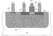
도 7에 도시된 본 발명의 다른 실시예는 실리콘 탄화물 또는 실리콘-게르마늄 탄화물과 같은 하이 밴드 갭 재료를 이용하여 게이트 접촉 영역(744)을 형성하는 것을 포함한다. 이러한 특징은 본 발명에서 게이트(640)-채널(650) 접합에 형성된 p-n 접합에서 장벽 높이를 증가시키기 위해 구현된다. 게이트 영역(640)에 인접하는 게이트 접촉 영역(744)의 하이 밴드 갭 재료는 게이트(640)-채널(650) 접합에 형성된 p-n 접합에서 장벽 높이를 효과적으로 증가시킨다. 보다 높은 게이트-채널 접합 내부 전위는 접합 양단의 포화 전류를 감소시키며, 많은 양의 게이트 전류가 게이트-채널 다이오드 양단에 흐르게 하지 않고 이 다이오드를 순방향 바이어싱하기 위해 이 다이오드에 적용될 수 있는 최대 전압을 증가를 허가한다. 게이트에서의 최대 전압은 인버터의 전원 전압과 동일하므로, 보다 높은 전원 전압이 가능하게 되어, 트랜지스터들의 구동 세기를 증가시키고, 인버터의 보다 빠른 스위칭이 달성된다. 본 실시예에 대해 도 7에 도시된 바와 같이, 전극을 형성하기 위해 폴리실리콘 대신에 폴리실리콘 탄화물 재료가 사용된다. 폴리실리콘 탄화물과 같은 하이 밴드 갭 재료의 사용은 게이트-채널 다이오드가 트랜지스터의 온 상태 동안 약하게 순방향 바이어싱될 때 게이트 접합의 누설 전류를 감소시킨다. 본 발명은 이러한 목적을 위해 실리콘 탄화물의 다양한 상태, 즉 3C, 4H 및 6H의 이용을 가르친다. 또한, 본 발명은 실리콘-게르마늄-탄소의 삼원소 합금 및 갈륨-알루미늄-비소화물-인화물과 같은 다양한 다른 화합물 반도체를 포함하는, 실리콘 기판과의 정류 접합을 형성하는 데 사용될 수 있는 다양한 다른 전극 재료의 사용을 가르친다. 본 발명의 다른 실시예에서, 실리콘 탄화물과 같은 게이트용 재료들의 사용은 실리콘-게르마늄과 같은 에피텍셜 피착된 고 이동도 재료들과 함께 동시에 이루어진다. 게이트 재료의 조성은 피착 동안 변한다. 730, 732, 744 및 752로 표시된 소스, 드레인, 게이트 및 웰 탭에 대한 전극 연장들은 실리콘 탄화물과 같은 하이 밴드 갭 반도체 재료로 이루어진다. 이러한 전극들의 상부에 자기 정렬 도전층이 형성되고, 750으로 표시된다. 이전 단락들에서 설명된 바와 같이, 다결정 반도체 재료들이 적절히 도핑된다. 트랜지스터들의 다른 컴포넌트들은 도 6에서 설명된 nJFET 구조와 유사하게 유지된다.Another embodiment of the present invention shown in FIG. 7 includes forming a
본 발명의 일 실시예는 10 Å 내지 1000 Å 범위의 깊이로 실리콘의 표면 근처에 실리콘-탄화물 층을 사용한 후 10 Å 내지 2500 Å의 깊이로 폴리실리콘을 피착하는 것을 가르친다. 다결정 층의 조성은 에칭 프로세스의 정확한 모니터링을 돕기 위해 변하는데, 이 프로세스에서는 층의 하부를 구분하는 조성이 검출될 때까지 다결정 재료가 빠르게 에칭된 후, 모든 다결정 재료가 에칭될 때까지 선택적 에칭 프로세스를 이용하여 느리게 에칭된다. 폴리실리콘 탄화물을 이용하는 제조 프로세스의 상세한 설명은 후술한다.One embodiment of the present invention teaches the use of a silicon-carbide layer near the surface of silicon to a depth in the range of 10 kV to 1000 kV and then depositing polysilicon to a depth of 10 kV to 2500 kV. The composition of the polycrystalline layer is changed to help accurate monitoring of the etching process, in which the polycrystalline material is etched rapidly until a composition that separates the bottom of the layer is detected, and then the selective etching process until all the polycrystalline materials are etched. Is slowly etched using. Detailed description of the manufacturing process using polysilicon carbide will be given later.
이어서, 도 5에 도시된 바와 같은 상보형 JFET 구조를 형성하는 예시적이고 비제한적인 방법이 도 9의 흐름도로서 도시된다. 흐름도의 각 단계는 도 10-20에 더 도시된다. 단계 905는 도 10에 도시된다. 단계 910은 도 11에 도시된다. 단계 915는 도 12에 도시된다. 단계 920 및 925는 도 13에 도시된다. 단계 930은 도 14에 도시된다. 단계 935는 도 15에 도시된다. 단계 940은 도 16에 도시된다. 단계 950은 도 17에 도시된다. 단계 955는 도 18에 도시된다. 단계 960은 도 19에 도시된다. 단계 965는 도 20에 도시된다.Subsequently, an exemplary, non-limiting method of forming a complementary JFET structure as shown in FIG. 5 is shown as the flowchart of FIG. 9. Each step of the flowchart is further illustrated in FIGS. 10-20. Step 905 is shown in FIG. 10. Step 910 is shown in FIG. 11. Step 915 is shown in FIG. 12.
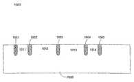
도 10은 에칭, 열 산화 및 실리콘 이산화물의 피착의 조합에 의해 능동 소자들이 형성되는 다양한 영역의 분리를 달성하기 위해 제조 동안의 예비 단계들이 완료된 후의 반도체 기판의 단면도를 나타낸다. 영역들(1001-1005)은 에칭, 피착 및 열 성장의 조합에 의해 실리콘 산화물 및 질화물로 구성된 절연 재료로 채워지는 영역들을 나타낸다. 이러한 영역들을 형성하기 위한 프로세스의 상세는 이 분야의 전문가들에게 잘 알려져 있으며, 본 발명의 범위 밖이다. 영역들(1011-1014)은 후속 단계들에서 능동 트랜지스터들이 형성되는 영역들을 나타낸다.FIG. 10 shows a cross-sectional view of a semiconductor substrate after preliminary steps during fabrication have been completed to achieve separation of various regions in which active elements are formed by a combination of etching, thermal oxidation, and deposition of silicon dioxide. Regions 1001-1005 represent regions filled with an insulating material composed of silicon oxide and nitride by a combination of etching, deposition and thermal growth. Details of the process for forming such areas are well known to those skilled in the art and are outside the scope of the present invention. Regions 1011-1014 represent regions in which active transistors are formed in subsequent steps.
도 11은 영역들(1101, 1102)에서 적절한 불순물로 활성 영역들을 도핑함으로써 n웰 및 p웰을 형성하는 단계를 나타낸다. 영역(1102) 내의 n웰에 대해, 인 또는 비소 원자들이 주입된다. 주입의 도핑 레벨은 1.0x1011cm2 내지 1.0x1014cm2 사이에서 변한다. 주입 에너지는 10 KeV 내지 400 KeV 사이에서 변한다. 영역(1101) 내의 p웰에 대해, 1.0x1011cm2 내지 1.0x1014cm2 사이에서 변하는 도스와 10 KeV와 400 KeV 사이에서 변하는 주입 에너지를 갖는 이온 주입에 의해 붕소가 주입된다. 원하는 불순물 도핑 프로파일을 얻기 위해 다수의 주입이 사용될 수 있다. n형 및 p형 불순물을 영역들에 선택적으로 주입하기 위하여, 주입을 받지 않도록 설계된 영역을 차단하기 위한 포토레지스트 마스크를 이용하여 주입이 행해진다. 산화물 아래의 영역에서의 도핑을 증가시켜 2개의 인접 n웰 사이의 임의의 누설을 방지하기 위하여 분리 영역들(1001-1005) 아래에 추가적인 붕소 주입이 행해진다. 원하는 불순물 도핑 프로파일을 얻기 위해 웨이퍼가 열처리된다.FIG. 11 illustrates forming n well and p well by doping active regions with appropriate impurities in
도 12a 및 12b는 각각 nJFET를 위한 채널 영역(1202) 및 pJFET를 위한 채널 영역(1222)의 형성을 나타낸다. 채널 영역은 포토레지스트 마스크를 이용하는 선택적 주입에 의해 형성된다. nJFET에 대해, 도 12a에 영역(1202)로 도시된 채널은 2.0x1011cm2 내지 1.0x1014cm2 의 주입 도스 및 1 KeV 내지 100 KeV의 주입 에너지를 갖는 비소, 인 또는 안티몬과 같은 n형 도펀트를 이용한 이온 주입에 의해 형성된다. 또한, 도면에는 n채널 주입이 차단되는 영역들을 커버하는 포토레지스트(1210)가 도시되어 있다. 도 12b의 영역(1222)은 pJFET의 채널을 형성하기 위해 붕소, 인듐 또는 탈륨과 같은 p형 불순물로 주입된다. 본 발명의 다른 실시예에서, 채널 영역은 플라즈마 이멀션 도핑에 의해 형성된다. 대안으로, 채널은 실리콘, 실리콘-게르마늄 이원 합금, 또는 실리콘-게르마늄-탄소 삼원 합금으로 구성되는 채널 영역의 에피텍셜 성장에 의해 형성된다. 본 발명은 n채널 및 p채널을 위한 채널 영역들의 선택적 에피텍셜 성장은 물론, nJFET 및 pJFET 양자를 위한 채널 영역들의 단일 피착에 이은 선택적 도핑에 의한 에피텍셜 영역들의 형성에 있어서의 변화들을 가르친다. 본 발명의 또 다른 실시예는 채널 영역들이 원자층 에피텍시와 같은 방법들에 의해 피착 동안 도핑되는 사례를 커버한다.12A and 12B show the formation of
이어서, 도 13에 도시된 바와 같이, 전체 웨이퍼 상에 폴리실리콘 층이 피착된다. 웨이퍼 상에 피착된 폴리실리콘의 두께는 100 Å 및 10,000 Å 사이에서 변한다. 폴리실리콘은 결국 JFET의 소스, 드레인, 게이트 및 웰 접촉들이 되는 영역들을 형성하기 위해 포토레지스트 마스크를 이용하여 선택적으로 도핑된다. 포토리소그라피 프로세스의 상세는 간명화를 위해 생략된다. 1300으로 도시된 바와 같이, 1310으로 표시된 영역은 1x10¹³/cm2 내지 1x10¹⁶/cm2범위의 도스의 고농도 붕소 주입을 이용하여 도핑된다. 이 영역은 nJFET의 웰 영역에 대한 접촉으로서 작용하도록 설계된다. 영역(1314)은 nJFET에 대한 게이트 접촉으로서 작용하도록 설계된다. 이 영역은 영역(1310)의 파라미터들과 유사한 파라미터들로 고농도로 p형 도핑된다. 영역들(1312, 1316)은 1x10¹³/cm2 내지 1x10¹⁶/cm2범위의 도스의 p형 도펀트(인, 비소 및 안티몬)로 고농도 도핑된다.Subsequently, as shown in FIG. 13, a polysilicon layer is deposited on the entire wafer. The thickness of the polysilicon deposited on the wafer varies between 100 GPa and 10,000 GPa. Polysilicon is selectively doped using a photoresist mask to form regions that eventually become source, drain, gate and well contacts of the JFET. Details of the photolithography process are omitted for simplicity. As shown at 1300, the area labeled 1310 ranges from 1x10¹³ / cm2 to 1x10¹⁶ / cm2. Doped using a high concentration of boron implant in a range of doses. This region is designed to act as a contact for the well region of the nJFET.
pJFET는 소스 및 드레인 접촉들(p형)로서 각각 작용하는 영역들(1320, 1324), 게이트(n형)로서의 영역(1322), 및 웰 탭(n형)에 대한 접촉으로서의 영역(1326)에 의해 형성된다. 영역들(1320, 1324)은 1x10¹³/cm2 내지 1x10¹⁶/cm2범위의 도스의 붕소 원자들로 고농도 도핑되며, pJFET의 소스 및 드레인 접촉들 각각으로서 작용하도록 설계된다. 마찬가지로, 영역들(1322, 1326)은 n형으로 고농도 도핑되며, pJFET의 게이트 및 웰 접촉들로서 작용하도록 설계된다. 다른 실시예에서, 이온 주입을 행하기 전에 폴리실리콘 층의 상부에 산화물 층이 피착된다. 이 층의 두께는 20 Å 내지 500 Å 사이에서 변한다. 다른 실시예에서, 이온 주입 전에 폴리실리콘의 상부에 산화물 및 질화물의 층들이 피착되는데, 산화물 및 질화물 막들의 두께는 10 Å에서 500 Å 사이에서 변한다.The pJFET has
도 14는 불순물이 도핑된 폴리실리콘 층, 및 폴리실리콘 층 상부의 보호층(1410)을 갖는 실리콘 웨이퍼의 단면도를 나타낸다. 다양한 영역에 불순물이 주입된 폴리실리콘 층은 웰에 대한 소스, 드레인 및 게이트 접합들 및 저항 접속들을 형성하기 위해 실리콘으로의 불순물의 간접 확산의 소스로서 사용된다. 영역들(1422, 1426)은 폴리실리콘 영역들(1312, 1316)로부터 확산된 nJFET의 소스 및 드레인 영역들이다. 영역(1424)은 n형 채널이다. 1428로 표시된 게이트 영역은 p형 도핑된 폴리실리콘으로부터 실리콘으로 확산된다. 영역(1420)은 폴리실리콘 영역(1310)으로부터의 확산에 의해 실리콘 내에 형성된 p형 영역(웰 탭)이며, nJFET를 포함하는 p웰에 대한 저항 접촉을 형성한다. 마찬가지로, 실리콘 내의 pJFET 접촉들은 pJFET의 소스로서의 영역(1430), 채널로서의 영역(1432), 드레인으로서의 영역(1434), 웰 접촉으로서의 영역(1436), 및 게이트 영역으로서의 영역(1438)에 의해 형성된다. 다른 실시예에서, 폴리실리콘 내의 n형 및 p형 도펀트들의 주입 도스 및 에너지가 변하는 다수의 이온 주입이 웰 접촉들, 소스, 드레인 및 게이트 영역들을 형성하도록 행해진다.FIG. 14 shows a cross-sectional view of a silicon wafer having a polysilicon layer doped with an impurity and a
JFET의 다양한 영역들의 실리콘으로의 확산 후에, 게이트 패터닝 프로세스가 행해진다. 광학 리소그라피 프로세스를 이용하여, 웨이퍼 상에 반사 방지 코팅층에 이어서 포토레지스트 층이 코팅된다. 이들 층의 두께는 이 분야의 전문가들에게 공지된 바와 같이 포토레지스트의 선택에 의존한다. 도 15에 1510으로 표시된 포토레지스트 층이 노광되어, 포토레지스트 내에 다양한 단자가 묘사된다. 본 발명의 다른 실시예는 임프린트 리소그라피 및 전자 빔 리소그라피를 포함하는 다른 포토레지스트 패터닝 방법들을 포함한다. 포토레지스트 층을 마스크로 이용하여, 폴리실리콘 위의 보호층이 먼저 에칭된다. 이어서, 폴리실리콘 층이 에칭되어, 1512와 같은 그루브들이 폴리실리콘 층의 하부에 도달한다. 이 단계는 15으로 도시된 바와 같이 다양한 단자를 전기적으로 분리한다. 포토레지스트의 패터닝을 위해, 광학 리소그라피, 이멀션 리소그라피, 임프린트 리소그라피, 직접 기입 전자 빔 리소그라피, X 레이 리소그라피, 또는 극자외선 리소그라피와 같은 다양한 프로세스가 이용된다.After diffusion of the various regions of the JFET into silicon, a gate patterning process is performed. Using an optical lithography process, an antireflective coating layer is subsequently coated on the wafer. The thickness of these layers depends on the choice of photoresist as is known to those skilled in the art. The photoresist layer labeled 1510 in FIG. 15 is exposed, depicting various terminals in the photoresist. Another embodiment of the present invention includes other photoresist patterning methods including imprint lithography and electron beam lithography. Using the photoresist layer as a mask, the protective layer over polysilicon is first etched. The polysilicon layer is then etched such that grooves such as 1512 reach the bottom of the polysilicon layer. This step electrically disconnects the various terminals as shown at 15. For the patterning of photoresists, various processes are used, such as optical lithography, emulsion lithography, imprint lithography, direct write electron beam lithography, X-ray lithography, or extreme ultraviolet lithography.
도 16a는 p채널 JFET의 게이트와 드레인/소스 간의 링크 영역을 도핑한 후의 실리콘 웨이퍼의 단면도이다. 폴리실리콘 층의 에칭 후, 소스와 채널, 및 드레인과 채널 사이에 저 전도도 경로를 형성하기 위해 고농도 도핑 영역들과 채널 사이의 영역이 도핑된다. 이를 링크 영역(1620, 1622, 1652, 1654)이라 한다. 도 16a는 pJFET의 링크 영역의 형성을 나타낸다. nJFET를 포함하는 웨이퍼의 섹션이 이 단계 동안 포토레지스트(1610)에 의해 커버되는 동안, pJFET의 링크 영역들(1620, 1622)을 도핑하기 위해 이온 주입 또는 플라즈마 이멀션 주입과 같은 적절한 도핑 프로세스가 이용된다. 링크 영역들은 이웃 소스 및 드레인 영역들의 접합 깊이와 무관한 접합 깊이로 형성되며, 소스/드레인과 채널 간의 매우 낮은 비저항 접속을 제공하도록 설계된다.16A is a cross-sectional view of a silicon wafer after doping the link region between the gate and drain / source of the p-channel JFET. After etching of the polysilicon layer, regions between the heavily doped regions and the channel are doped to form a low conductivity path between the source and the channel and the drain and the channel. These are referred to as
도 16b는 n채널 JFET의 게이트와 드레인/소스 간의 링크 영역의 도핑 후의 실리콘 웨이퍼의 단면도이다. 물체 1650은 주입이 차단되는, pJFET를 포함하는 영역들을 커버하는 포토레지스트이다. 실리콘 내의 영역들(1652, 1654)은 n형 도펀트들의 주입에 의해 형성된 링크 영역들이다. 이온 주입 후, 도펀트들은 고속 열 어닐링 프로세스에 의해 활성화된다. 에칭 동안 손상된 실리콘 영역을 산화하기 위해 700℃ 내지 950℃ 범위의 온도에서 10초 내지 20분 범위의 시간 동안의 산화 단계가 또한 수행된다.16B is a cross-sectional view of a silicon wafer after doping of the link region between the gate and drain / source of an n-channel JFET.
도 17은 폴리실리콘 블록들 간의 갭이 실리콘 이산화물과 같은 절연 재료로 채워진 다음, 폴리실리콘 층과 동일한 레벨의 거의 평면인 표면을 제공하기 위해 기계 화학적 연마와 같은 방법을 이용하여 처리된 후의 실리콘 웨이퍼의 단면도를 나타낸다. 화학 기상 증착 또는 플라즈마 지원 화학 기상 증착을 이용하여 실리콘 이산화물을 피착함으로써 폴리실리콘 블록들 사이에 절연 재료를 채우는 기술은 반도체 제조에 널리 사용되는 기술이다. 이러한 하나의 프로세스는 가스 형태의 실란과 산소 간의 저온 플라즈마 활성 반응에 의한 산화물의 피착을 이용한다. 베어 실리콘(bare silicon) 표면을 노출시키기 위해 보호층(1410)이 최종 제거된다.17 shows a silicon wafer after the gaps between polysilicon blocks are filled with an insulating material such as silicon dioxide and then processed using a method such as mechanical chemical polishing to provide a near planar surface at the same level as the polysilicon layer. The cross section is shown. BACKGROUND OF THE INVENTION The technique of filling an insulating material between polysilicon blocks by depositing silicon dioxide using chemical vapor deposition or plasma assisted chemical vapor deposition is a technique widely used in semiconductor manufacturing. One such process utilizes the deposition of oxides by low temperature plasma active reactions between silane and oxygen in gaseous form. The
도 18은 노출된 폴리실리콘 표면 상의 자기 정렬 실리사이드의 형성 후의 실리콘 웨이퍼의 단면도이다. 니켈, 코발트, 티타늄, 백금, 팔라듐 또는 다른 고융점 재료와 같은 금속의 층이 폴리실리콘 표면 상에 피착되고, 노출된 폴리실리콘 영역이 "금속 실리사이드"라고 하는 금속층과의 이원 화합물을 형성하도록 어닐링된다. 금속 실리사이드는 전도도가 매우 높은 재료이다. 피착된 금속의 바람직한 두께는 아주 깨끗한 폴리실리콘 표면 상에서 50 Å 내지 1000 Å 사이이다. 웨이퍼는 고속 어닐 노에서 200℃ 내지 800℃ 사이의 온도로 10초 내지 30분 동안 가열되어, 금속이 실리콘 또는 폴리실리콘 층과 접촉하는 곳에서 선택적으로 실리사이드가 형성된다. 금속층과 실리콘 간의 반응이 일어날 후, 실리사이드 층에 영향을 주지 않는 화학적 에칭 프로세스에 의해 웨이퍼로부터 잉여 금속이 제거된다. 반응하지 않은 금속은 적절한 용매를 이용하여 선택적으로 에칭되어, 노출된 실리콘 및 폴리실리콘 영역들(1801) 상에는 금속 실리사이드만이 남는다. 티타늄 및 코발트에 대해, 실온 이상의 온도도 사용될 수 있지만, 실온에서 적절한 경우에 과산화수소 및 수산화암모늄의 혼합물이 1:0.1 내지 1:10의 비율로 사용된다. 따라서, 자기 정렬 실리사이드 층이 폴리실리콘 상에 형성된다. 도 18은 폴리실리콘 소스, 드레인, 게이트 및 웰 탭 단자들 상의 실리사이드의 형성 후의 소자의 단면도를 나타낸다. 이러한 폴리실리콘 층은 로컬 상호접속으로도 사용되며, 이에 의해 실리사이드화된 n형 폴리실리콘 및 p형 폴리실리콘의 영역들이 저항 접촉들을 형성하는 데 사용된다.18 is a cross-sectional view of a silicon wafer after formation of self-aligned silicide on the exposed polysilicon surface. A layer of metal, such as nickel, cobalt, titanium, platinum, palladium or other high melting point material, is deposited on the polysilicon surface and the exposed polysilicon region is annealed to form a binary compound with a metal layer called "metal silicide". . Metal silicides are very conductive materials. The preferred thickness of the deposited metal is between 50 kPa and 1000 kPa on a very clean polysilicon surface. The wafer is heated in a high speed anneal furnace to a temperature between 200 ° C. and 800 ° C. for 10 seconds to 30 minutes to selectively form silicide where the metal is in contact with the silicon or polysilicon layer. After the reaction between the metal layer and silicon occurs, excess metal is removed from the wafer by a chemical etching process that does not affect the silicide layer. The unreacted metal is selectively etched using a suitable solvent, leaving only metal silicide on the exposed silicon and
다음 프로세스 단계는 유전체(산화물) 층을 피착하고, 산화물 층에 접촉 홀들을 에칭하고, 소스, 드레인, 게이트 및 웰 탭 단자들에 대한 접촉 홀들을 형성하고, 반도체 칩들의 형성시에 실시되는 바와 같은 통상의 금속 상호접속 형성 프로세스를 계속하는 것으로 구성된다. 유전체 피착 및 접촉 홀 에칭 후의 웨이퍼의 단면도가 도 19에 도시된다. 금속 피착 및 에칭이 도 20에 도시된다.The next process step is to deposit a dielectric (oxide) layer, etch contact holes in the oxide layer, form contact holes for source, drain, gate and well tap terminals, and as performed in the formation of semiconductor chips. It continues with the usual metal interconnect formation process. A cross-sectional view of the wafer after dielectric deposition and contact hole etching is shown in FIG. 19. Metal deposition and etching are shown in FIG. 20.
이 프로세스는 MOS 트랜지스터를 JFET와 함께 형성하는 데 적합할 수 있다. 이러한 적합화의 하나의 응용은 칩 상에 CMOS 호환 I/O들을 포함하는 것이다. MOS 트랜지스터를 형성하기 위한 프로세스는 다음에 설명된다. 도 21은 JFET 및 MOSFET의 n웰 및 p웰의 형성 후의 웨이퍼의 단면도를 나타낸다. MOSFET를 위한 임계 전압(Vt) 조정 주입 또한 완료된다. 게다가, JFET를 위한 채널 영역들의 형성 또한 완료된다. 웨이퍼 상에 게이트 유전체(산화물 또는 질화된 산화물) 층이 성장된다. 이 산화물 층은 MOSFET의 게이트를 둘러싸는 영역을 제외하고 웨이퍼로부터 에칭된다. 이 산화물 층은 물체 2110으로 도시된다. 본 발명의 다른 실시예에서, 산화물이 성장된 직후에 게이트 유전체의 상부에 비정질 실리콘의 얇은 층이 피착된다. 이 비정질 층의 두께는 다음 포토마스킹 및 에칭 단계 동안 하부의 게이트 유전체에 대한 손상을 방지하기에 충분하다. 이 비정질 층의 바람직한 두께는 10 Å 내지 5000 Å이다. 본 발명의 다른 실시예에서, 산화물 층이 먼저 형성되고, JFET의 채널이 후에 형성된다.This process may be suitable for forming MOS transistors with JFETs. One application of this adaptation is to include CMOS compatible I / Os on a chip. The process for forming a MOS transistor is described next. 21 shows a cross-sectional view of the wafer after formation of the n well and p well of the JFET and MOSFET. Threshold voltage (Vt) regulated injection for the MOSFETs is also complete. In addition, the formation of channel regions for the JFET is also completed. A gate dielectric (oxide or nitrided oxide) layer is grown on the wafer. This oxide layer is etched from the wafer except for the region surrounding the gate of the MOSFET. This oxide layer is shown as
이어서, 도 22에 도시된 바와 같이 웨이퍼 상에 폴리실리콘 층이 피착된다. 폴리실리콘 층은 2220으로 표시된 산화물의 보호층에 의해 커버된다. 웨이퍼 상의 소정 영역들을 정의하는 포토리소그라피에 의해, 웨이퍼로부터 포토레지스트 층이 선택적으로 제거되고, 노출된 영역들이 n형 및 p형 도펀트들로 주입된다. 이 도면은 선택적으로 도핑된 영역들을 가진 폴리실리콘 층을 나타낸다. 영역(2210)은 p형 도핑되고, 영역(2212)은 n형 도핑되고, 영역(2214)은 p형 도핑되고, 영역(2216)은 n형 도핑된다. 이러한 영역들의 도핑을 위한 파라미터들은 도 13에서 설명된 파라미터들과 동일하다.Subsequently, a polysilicon layer is deposited on the wafer as shown in FIG. 22. The polysilicon layer is covered by a protective layer of oxide labeled 2220. By photolithography defining certain regions on the wafer, the photoresist layer is selectively removed from the wafer and the exposed regions are implanted with n-type and p-type dopants. This figure shows a polysilicon layer with selectively doped regions.
다음 단계는 도 23에 도시된 바와 같은 폴리실리콘 상의 게이트 및 나머지 전극들의 정의이다. 이것은 포토레지스트 층(2330)에 패턴을 먼저 정의함으로써 달성된다. 이어서, 포토레지스트 층을 마스크로 이용하여, 폴리실리콘 층을 에칭하여, 전극들을 정의한다. 영역(2310)은 NMOS의 웰 탭을 형성하고, 영역(2312)은 NMOS의 소스를 형성하고, 영역(2314)은 NMOS의 게이트를 형성하고, 영역(2316)은 NMOS의 드레인을 형성하고, 영역(2320)은 PMOS의 소스를 형성하고, 영역(2322)는 PMOS의 게이트를 형성하고, 영역(2324)는 PMOS의 드레인의 드레인 영역을 형성하고, 영역(2326)은 PMOS의 웰 탭을 형성한다. 폴리실리콘 층의 에칭 후, 짧은 산화 사이클을 실행하여, 실리콘의 표면 상에 20 Å 내지 500 Å 두께의 산화물을 형성한다. 추가 가열 사이클을 실행하여, 폴리실리콘으로부터 게이트 유전체로 그리고 채널 영역으로의 도펀트들의 확산을 제어하면서, 드레인, 소스 및 웰 탭 영역들에서 폴리실리콘으로부터 실리콘으로의 도펀트들을 확산시킨다.The next step is the definition of the gate and the remaining electrodes on polysilicon as shown in FIG. This is accomplished by first defining a pattern in
도 24는 이온 주입에 의한 소스, 드레인 및 채널 영역들 간의 링크의 형성을 나타낸다. NMOS에 대해, 소스와 채널 및 드레인과 채널 간의 링크들은 2410 및 2412로 각각 표시된 n형 도펀트들의 이온 주입에 의해 형성된다. PMOS에 대해, 소스와 채널 및 드레인과 채널 간의 링크들은 2420 및 2422로 각각 표시된 p형 도펀트들의 이온 주입에 의해 형성된다. 주입을 활성화하기 위해 고속 열 어닐이 수행된다. 웨이퍼의 단면은 도 17에 도시된 것과 매우 유사하다. 웨이퍼는 도 17 내지 20에서 설명되는 방법에 의해 처리된다.24 illustrates the formation of a link between source, drain and channel regions by ion implantation. For NMOS, the links between the source and channel and the drain and channel are formed by ion implantation of n-type dopants labeled 2410 and 2412, respectively. For PMOS, the links between the source and channel and the drain and channel are formed by ion implantation of p-type dopants, denoted 2420 and 2422, respectively. Fast thermal annealing is performed to activate the implant. The cross section of the wafer is very similar to that shown in FIG. The wafer is processed by the method described in FIGS. 17-20.
동일 웨이퍼 상에 JFET 및 MOSFET를 형성하는 완전한 흐름이 도 25에 도시되어 있다. 이러한 방식으로 제조되는 MOS 트랜지스터는 여기에 설명되는 바와 같이 MOS 트랜지스터를 형성하는 종래의 방법에 비해 많은 이점을 갖는다.The complete flow of forming a JFET and a MOSFET on the same wafer is shown in FIG. 25. MOS transistors manufactured in this manner have a number of advantages over conventional methods of forming MOS transistors as described herein.
종래의 MOS 트랜지스터는 고농도로 도핑된 소스/드레인 영역을 게이트로부터 분리하는 데 사용되는 스페이서를 갖는다. 스페이서의 치수는 수직 폴리실리콘 치수 및 다른 처리 파라미터들에 의존하며, 측면으로는 축소될 수 없다. MOS 트랜지스터의 본 실시예는 리소그라피를 이용하여 소스/드레인 및 게이트 영역을 분리하여, 이 구조를 측면으로 축소 가능하게 한다.Conventional MOS transistors have spacers that are used to separate heavily doped source / drain regions from the gate. The dimension of the spacer depends on the vertical polysilicon dimension and other processing parameters and cannot be reduced laterally. This embodiment of the MOS transistor uses lithography to separate the source / drain and gate regions, making this structure laterally shrinkable.
종래의 MOS 트랜지스터는 스페이서 아래에 저농도로 도핑된 소스 및 드레인 영역을 가지며, 이는 소스의 주입 효율, 또는 트랜지스터에 의해 제어될 수 있는 최대 전류를 제한한다. MOS 트랜지스터의 본 실시예는 링크 영역을 소스 및 드레인 접합들로 이용하며, 이러한 영역의 도핑이 독립적으로 제어되는 것을 가능하게 한다.Conventional MOS transistors have a lightly doped source and drain region under the spacer, which limits the implantation efficiency of the source, or the maximum current that can be controlled by the transistor. This embodiment of the MOS transistor uses the link region as the source and drain junctions, and allows the doping of this region to be controlled independently.
종래의 MOS 트랜지스터는 대칭적인 소스 및 드레인 영역을 갖는다. 본 실시예는 소스 및 드레인 폴리실리콘 영역을 게이트로부터 비대칭적으로 이격시킴으로써 비대칭적인 소스 및 드레인 접합이 형성되는 것을 가능하게 한다.Conventional MOS transistors have symmetrical source and drain regions. This embodiment enables asymmetrical source and drain junctions to be formed by asymmetrically separating the source and drain polysilicon regions from the gate.
종래의 MOS 트랜지스터는 소스/드레인 및 게이트 단자들에 대한 다양한 접촉 깊이를 가지며, 소스/드레인 단자들에 대한 접촉들은 실리콘에 대해 직접 이루어지는 반면, 게이트 단자에 대한 접촉은 소스/드레인 접합들로부터 상승된 폴리실리콘에 대해 이루어진다. MOS 트랜지스터의 본 실시예는 모든 접촉 홀들을 폴리실리콘까지 에칭하여, 모든 홀의 깊이를 동일하게 유지한다.Conventional MOS transistors have varying contact depths for source / drain and gate terminals, while contacts to source / drain terminals are made directly to silicon, while contact to gate terminal is raised from source / drain junctions. Made for polysilicon. This embodiment of the MOS transistor etches all contact holes up to polysilicon, keeping the depths of all holes the same.
종래의 MOS 트랜지스터는 얕은 소스/드레인 접합 및 이들 접합 상부의 실리사이드 형성에 의해 부과되는 제한으로 인해 단채널 성능을 양보하여야 한다. MOS 트랜지스터의 본 실시예는 모든 접합에 대해 폴리실리콘의 상부에 실리사이드를 배치함으로써 이러한 제한을 제거한다. 또한, 실리콘 내의 얕은 소스/드레인 접합은 폴리실리콘으로부터의 도펀트 확산에 의해 형성되며, 이는 보다 느리고 보다 제어 가능한 프로세스이다.Conventional MOS transistors must yield short channel performance due to the limitations imposed by shallow source / drain junctions and silicide formation on top of these junctions. This embodiment of the MOS transistor removes this limitation by placing silicide on top of polysilicon for all junctions. In addition, shallow source / drain junctions in silicon are formed by dopant diffusion from polysilicon, which is a slower and more controllable process.
JFET 및 MOSFET를 형성하는 본 방법은 접촉 홀 에칭 전에 평면이 존재하는 것을 가능하게 한다. 이것은 또한 제거되는 폴리실리콘의 양이 제한되는 것을 보증하는데, 이는 균일한 플라즈마 에칭을 달성하는 데 중요하다. 실리콘 웨이퍼 상의 폴리실리콘 패턴의 밀도 변화가 폴리실리콘의 에칭 레이트의 변화의 원인인 것으로 알려져 있다. 본 방법에서, 이 문제는 폴리실리콘의 패턴 밀도가 종래의 프로세스 기술에서보다 훨씬 높다는 사실에 의해 극복된다. 또한, 다양한 접합에 대한 접촉들은 폴리실리콘 층에 의해 분리되며, 이는 얕은 소스 및 드레인 접합을 형성하는 것을 매우 편리하게 한다.The present method of forming JFETs and MOSFETs allows the plane to exist before contact hole etching. This also ensures that the amount of polysilicon removed is limited, which is important for achieving uniform plasma etching. It is known that the change in density of the polysilicon pattern on the silicon wafer is the cause of the change in the etching rate of the polysilicon. In this method, this problem is overcome by the fact that the pattern density of polysilicon is much higher than in conventional process technology. In addition, the contacts for the various junctions are separated by a polysilicon layer, which makes it very convenient to form shallow source and drain junctions.
도 25의 단계들은 도 26-30에 더 설명된다.The steps of FIG. 25 are further described in FIGS. 26-30.
도 26은 분리 영역들(2610), 2601로 표시된 NMOS 트랜지스터를 형성하기 위한 p웰 및 2602로 표시된 nJFET를 형성하기 위한 다른 p웰의 형성 후의 실리콘 웨이퍼의 단면도를 나타낸다. PMOS 트랜지스터 및 pJFET를 형성하기 위한 대응하는 웰 구조도 형성되지만, 간명화를 위해 생략된다. MOS 트랜지스터를 위해 실리콘 내의 Vt 조정 주입이 수행된 후에, 전체 웨이퍼에 대해 게이트 산화가 수행되고, 10 Å 내지 100 Å 범위의 적절한 두께의 게이트 유전체 층이 웨이퍼 상에 성장된다. 이것은 도면에서 층(2620)으로 도시되어 있다. 본 발명의 다른 실시예에서, 게이트 유전체는 하프늄 실리케이트 및 이 분야의 전문가들에게 공지된 유사한 재료와 같은 고 유전율 재료로 형성된다.FIG. 26 shows a cross-sectional view of a silicon wafer after formation of
도 27은 다음 단계들이 수행된 후의 웨이퍼의 단면도를 나타낸다. 먼저, 습식 에칭 또는 플라즈마 에칭과 같은 적절한 기술에 의해, JFET 채널이 형성될 영역들로부터 선택적으로 게이트 유전체가 제거된다. 이어서, 이온 주입에 의해 물체 2710으로 표시된 JFET 채널이 형성된다. 채널 형성 후, 웨이퍼 상에 다결정 재료의 층이 피착된다. 이것은 2720으로 표시된다.27 shows a cross-sectional view of the wafer after the following steps have been performed. First, by appropriate techniques such as wet etching or plasma etching, the gate dielectric is selectively removed from the regions where the JFET channel is to be formed. Ion implantation then forms a JFET channel, represented by
JFET 및 MOS 트랜지스터의 게이트 전극들에는 적절한 도펀트가 주입된다. NMOS 트랜지스터 및 pJFET의 게이트 영역들은 비소, 인 또는 안티몬으로 고농도로 p형 도핑된다. PMOS 및 nJFET의 게이트 전극 영역들에는 p형 도펀트, 즉 붕소가 주입된다. 게이트 전극 영역들은 1x10¹⁴/cm2 내지 1x10¹⁶/cm2 범위의 도펀트들의 고농도 도스로 주입된다. 본 발명의 다른 실시예는 MOS 및 JFET 트랜지스터의 게이트 전극 영역을 형성하기 위한 다수의 주입 단계를 포함한다. 웨이퍼는 폴리실리콘 층 전체에 도펀트들을 분배하기 위해 가열된다.Appropriate dopants are implanted into the gate electrodes of the JFET and MOS transistors. The gate regions of the NMOS transistor and pJFET are heavily p-doped with arsenic, phosphorus or antimony. The p-type dopant, ie, boron, is implanted into the gate electrode regions of the PMOS and nJFET. The gate electrode regions are implanted with a high dose of dopants in the range of1 ×1014 / cm2 to 1 × 10¹⁶ / cm2 . Another embodiment of the present invention includes a number of implantation steps for forming gate electrode regions of MOS and JFET transistors. The wafer is heated to distribute the dopants throughout the polysilicon layer.
웨이퍼 상에 포토마스크가 배치되고, 폴리실리콘 층이 에칭되어, 도 28에 도시된 바와 같이 트랜지스터용 게이트 전극이 정의된다. 물체 2810은 NMOS 트랜지스터의 게이트를 형성하고, 물체 2820은 nJFET 트랜지스터의 게이트 전극을 형성한다. NMOS 트랜지스터의 게이트는 n형 폴리실리콘으로 형성되고, nJFET의 게이트는 p형 폴리실리콘으로 형성된다. 게이트의 정의 후, 짧은 산화 사이클을 수행하여 폴리실리콘 표면으로부터 손상을 제거한다. 이어서, 산화물 및 질화물의 층들이 피착되고, 이방성으로 에칭되어 게이트 전극에 인접하는 스페이서가 형성된다. 스페이서 형성의 종료시에, 웨이퍼의 단면은 양 측면이 스페이서로 둘러싸인 게이트 전극을 보인다. 2830으로 표시된 물체는 게이트를 둘러싸는 스페이서이다. nJFET 섬(2602) 상의 폴리실리콘은 하부에 에칭을 중지시키기 위한 산화물 층을 갖지 않음에 유의해야 한다. 따라서, 폴리실리콘 에칭 프로세스는 폴리실리콘을 오버 에칭하여 실리콘을 에칭하지 않도록 매우 주의 깊게 수행되어야 한다. 폴리실리콘의 오버 에칭을 방지하기 위한 프로세스 단계들은 전술하였다.A photomask is placed on the wafer and the polysilicon layer is etched to define a gate electrode for the transistor as shown in FIG.
도 29는 MOS 및 JFET 트랜지스터를 위한 소스 및 드레인 영역이 형성된 후의 실리콘 웨이퍼의 단면도를 나타낸다. 프로세스 단계는 NMOS 트랜지스터를 위한 저농도 도핑 드레인(LDD) 영역을 형성하는 단계로 구성된다. 이것은 NMOS 영역(2601) 내의 n형 도펀트의 선택적 이온 주입에 의해 행해진다. 이 단계는 또한 드레인 및 소스의 공핍 영역들이 서로 접촉하여 "펀치 스루"로 알려진 현상이 발생하는 것을 방지하기 위한 반대 극성(p형)의 도펀트의 주입을 수반한다. 이 단계는 "펀치 스루 방지" 주입으로 알려져 있다. LDD 및 펀치 스루 방지 주입은 완전 수직 내지 수직으로부터 60%의 경사 범위의 웨이퍼 상의 입사각으로 수행된다. 이러한 영역들은 도 29에 2910으로 표시된다. JFET의 채널과 소스 및 드레인 영역들 사이에 저저항 영역(링크)을 형성하기 위해 유사한 프로세스가 수행된다. 물체들 2920으로 표시된 링크들은 JFET의 게이트에 인접 형성된다. NMOS 및 nJFET 트랜지스터들 양자에 대해 소스 및 드레인 영역들은 n형 불순물의 이온 주입에 의해 형성된다. NMOS 용의 소스 및 드레인 단자들을 형성하기 위한 n형 이온 주입은 양호하게 확립된 프로세스이다. nJFET에 대해, 소스 및 드레인의 도핑 타입은 게이트의 도핑 타입과 반대이다. 소스 및 드레인의 주입 파라미터들은 이들 단자를 형성하는 데 사용되는 n형 도펀트들이 게이트 영역의 극성을 반전시키지 않는 것을 보장하도록 조정된다. JFET를 위한 게이트 도핑은 n 또는 p형 도펀트들을 1x10¹⁴/cm2 내지 1x10¹⁶/cm2 의 도스로 주입함으로써 높은 레벨로 유지된다. 주입 에너지를 폴리실리콘 두께에 기초하여 선택된다. JFET의 소스 및 드레인의 도핑은 게이트 도핑의 반전이 발생하지 않는 것을 보장하기 위해 게이트 도핑보다 낮게 유지된다. NMOS 트랜지스터의 소스 및 드레인 영역들은 2950 및 2952로 표시되며, nJFET의 소스 및 드레인은 각각 2954 및 2956으로 표시된다.29 shows a cross-sectional view of a silicon wafer after source and drain regions have been formed for MOS and JFET transistors. The process step consists in forming a low concentration doped drain (LDD) region for the NMOS transistor. This is done by selective ion implantation of the n-type dopant in the
도 30a는 접촉 홀들 및 금속 접속들이 형성된 후의 실리콘 웨이퍼의 단면도를 나타낸다. 소스 및 드레인의 형성에 이어서, 코발트, 니켈, 티타늄, 백금 등과 같은 금속 층을 피착하고, 웨이퍼를 가열하여 금속이 노출된 실리콘 표면과 반응하는 것을 허가하여 실리사이드 화합물을 형성함으로써 자기 정렬 실리사이드 형성이 이루어진다. 사용되지 않은 금속은 습식 케미컬 에칭에 의해 제거된다. 이어서, 도 30a에 도시된 바와 같이 전체 웨이퍼를 커버하기 위한 유전체로서 600℃ 이하의 온도에서 산화물 층을 피착한다. 유전체 층 내에 접촉 홀들(3010)이 에칭된다. 단일 또는 다수 층의 금속 합금이 웨이퍼 상에 피착되고, 포토리소그라피 프로세스에 의해 패터닝된 후, 금속 층을 에칭하여 물체 3020으로 도시된 트랜지스터들로부터의 상호접속들을 형성한다. NMOS 및 nJFET의 레이아웃이 도 30b에 도시되어 있다. NMOS 트랜지스터의 소스, 드레인 및 게이트 영역들은 3050, 3051 및 3054로 표시된다. 이들 각각의 접촉 홀은 3060, 3061 및 3064로 표시된다. 마찬가지로, nJFET의 소스, 드레인 및 게이트 영역들은 물체들 3052, 3053 및 3055로 표시되며, 이들의 접촉 홀은 각각 3062, 3063 및 3065로 표시된다.30A shows a cross-sectional view of a silicon wafer after contact holes and metal connections are formed. Following formation of the source and drain, self-aligned silicide formation is achieved by depositing a metal layer, such as cobalt, nickel, titanium, platinum, and the like, and heating the wafer to allow the metal to react with the exposed silicon surface to form a silicide compound. . Unused metal is removed by wet chemical etching. Subsequently, an oxide layer is deposited at a temperature of 600 ° C. or lower as a dielectric for covering the entire wafer as shown in FIG. 30A. Contact holes 3010 are etched in the dielectric layer. After a single or multiple layers of metal alloy are deposited on the wafer and patterned by a photolithography process, the metal layer is etched to form interconnects from the transistors shown as
Claims (68)
Translated fromKoreanApplications Claiming Priority (2)
| Application Number | Priority Date | Filing Date | Title |
|---|---|---|---|
| US11/261,873US7569873B2 (en) | 2005-10-28 | 2005-10-28 | Integrated circuit using complementary junction field effect transistor and MOS transistor in silicon and silicon alloys |
| US11/261,873 | 2005-10-28 |
Publications (1)
| Publication Number | Publication Date |
|---|---|
| KR20080076915Atrue KR20080076915A (en) | 2008-08-20 |
Family
ID=37995097
Family Applications (1)
| Application Number | Title | Priority Date | Filing Date |
|---|---|---|---|
| KR1020087012745ACeasedKR20080076915A (en) | 2005-10-28 | 2006-10-30 | Integrated Circuit Using Complementary Junction Field Effect Transistor and MOOS Transistor in Silicon and Silicon Alloys |
Country Status (8)
| Country | Link |
|---|---|
| US (3) | US7569873B2 (en) |
| EP (1) | EP1949456A4 (en) |
| JP (1) | JP2009514233A (en) |
| KR (1) | KR20080076915A (en) |
| CN (2) | CN102332472A (en) |
| CA (1) | CA2626706A1 (en) |
| TW (1) | TWI333695B (en) |
| WO (1) | WO2007053485A2 (en) |
Cited By (1)
| Publication number | Priority date | Publication date | Assignee | Title |
|---|---|---|---|---|
| US9425104B2 (en) | 2013-09-06 | 2016-08-23 | Samsung Electronics Co., Ltd. | Complementary metal oxide semiconductor device and method of manufacturing the same |
Families Citing this family (113)
| Publication number | Priority date | Publication date | Assignee | Title |
|---|---|---|---|---|
| US8957511B2 (en) | 2005-08-22 | 2015-02-17 | Madhukar B. Vora | Apparatus and methods for high-density chip connectivity |
| US7745301B2 (en) | 2005-08-22 | 2010-06-29 | Terapede, Llc | Methods and apparatus for high-density chip connectivity |
| US7592841B2 (en)* | 2006-05-11 | 2009-09-22 | Dsm Solutions, Inc. | Circuit configurations having four terminal JFET devices |
| US7569873B2 (en)* | 2005-10-28 | 2009-08-04 | Dsm Solutions, Inc. | Integrated circuit using complementary junction field effect transistor and MOS transistor in silicon and silicon alloys |
| TW200805882A (en)* | 2005-12-07 | 2008-01-16 | Dsm Solutions Inc | Method of producing and operating a low power junction field effect transistor |
| US9159568B2 (en)* | 2006-02-04 | 2015-10-13 | Cypress Semiconductor Corporation | Method for fabricating memory cells having split charge storage nodes |
| US7764137B2 (en)* | 2006-09-28 | 2010-07-27 | Suvolta, Inc. | Circuit and method for generating electrical solutions with junction field effect transistors |
| US20080099798A1 (en)* | 2006-10-31 | 2008-05-01 | Douglas Kerns | Methods and devices for amplifying a signal |
| US7525163B2 (en)* | 2006-10-31 | 2009-04-28 | Dsm Solutions, Inc. | Semiconductor device, design method and structure |
| US20080099796A1 (en)* | 2006-11-01 | 2008-05-01 | Vora Madhukar B | Device with patterned semiconductor electrode structure and method of manufacture |
| US20080237657A1 (en)* | 2007-03-26 | 2008-10-02 | Dsm Solution, Inc. | Signaling circuit and method for integrated circuit devices and systems |
| US20080265936A1 (en)* | 2007-04-27 | 2008-10-30 | Dsm Solutions, Inc. | Integrated circuit switching device, structure and method of manufacture |
| US7729149B2 (en)* | 2007-05-01 | 2010-06-01 | Suvolta, Inc. | Content addressable memory cell including a junction field effect transistor |
| US20080272401A1 (en)* | 2007-05-03 | 2008-11-06 | Dsm Solutions, Inc. | Inverted Junction Field Effect Transistor and Method of Forming Thereof |
| US7531854B2 (en) | 2007-05-04 | 2009-05-12 | Dsm Solutions, Inc. | Semiconductor device having strain-inducing substrate and fabrication methods thereof |
| US7453107B1 (en)* | 2007-05-04 | 2008-11-18 | Dsm Solutions, Inc. | Method for applying a stress layer to a semiconductor device and device formed therefrom |
| US7772056B2 (en)* | 2007-06-18 | 2010-08-10 | University Of Utah Research Foundation | Transistors for replacing metal-oxide semiconductor field-effect transistors in nanoelectronics |
| US7629812B2 (en)* | 2007-08-03 | 2009-12-08 | Dsm Solutions, Inc. | Switching circuits and methods for programmable logic devices |
| US8035139B2 (en)* | 2007-09-02 | 2011-10-11 | Suvolta, Inc. | Dynamic random access memory having junction field effect transistor cell access device |
| US7704844B2 (en)* | 2007-10-04 | 2010-04-27 | International Business Machines Corporation | High performance MOSFET |
| US20090168508A1 (en)* | 2007-12-31 | 2009-07-02 | Dsm Solutions, Inc. | Static random access memory having cells with junction field effect and bipolar junction transistors |
| US8207784B2 (en) | 2008-02-12 | 2012-06-26 | Semi Solutions, Llc | Method and apparatus for MOSFET drain-source leakage reduction |
| US7688117B1 (en) | 2008-04-21 | 2010-03-30 | The United States Of America As Represented By The Administrator Of National Aeronautics And Space Administration | N channel JFET based digital logic gate structure |
| US7710148B2 (en)* | 2008-06-02 | 2010-05-04 | Suvolta, Inc. | Programmable switch circuit and method, method of manufacture, and devices and systems including the same |
| US8120072B2 (en) | 2008-07-24 | 2012-02-21 | Micron Technology, Inc. | JFET devices with increased barrier height and methods of making same |
| US8232585B2 (en) | 2008-07-24 | 2012-07-31 | Micron Technology, Inc. | JFET devices with PIN gate stacks |
| US20100019289A1 (en)* | 2008-07-25 | 2010-01-28 | Dsm Solutions, Inc. | Junction Field Effect Transistor Using Silicide Connection Regions and Method of Fabrication |
| US8278691B2 (en) | 2008-12-11 | 2012-10-02 | Micron Technology, Inc. | Low power memory device with JFET device structures |
| US8481372B2 (en)* | 2008-12-11 | 2013-07-09 | Micron Technology, Inc. | JFET device structures and methods for fabricating the same |
| US7943971B1 (en) | 2008-12-17 | 2011-05-17 | Suvolta, Inc. | Junction field effect transistor (JFET) structure having top-to-bottom gate tie and method of manufacture |
| US8421162B2 (en) | 2009-09-30 | 2013-04-16 | Suvolta, Inc. | Advanced transistors with punch through suppression |
| US8273617B2 (en) | 2009-09-30 | 2012-09-25 | Suvolta, Inc. | Electronic devices and systems, and methods for making and using the same |
| JP5126245B2 (en)* | 2010-02-12 | 2013-01-23 | 株式会社デンソー | Silicon carbide semiconductor device having complementary junction field effect transistor and method of manufacturing the same |
| US8530286B2 (en) | 2010-04-12 | 2013-09-10 | Suvolta, Inc. | Low power semiconductor transistor structure and method of fabrication thereof |
| US8329568B1 (en)* | 2010-05-03 | 2012-12-11 | Xilinx, Inc. | Semiconductor device and method for making the same |
| CN102254818B (en)* | 2010-05-19 | 2013-05-01 | 中国科学院微电子研究所 | Semiconductor junction diode device and manufacturing method thereof |
| US8569128B2 (en) | 2010-06-21 | 2013-10-29 | Suvolta, Inc. | Semiconductor structure and method of fabrication thereof with mixed metal types |
| US8377783B2 (en) | 2010-09-30 | 2013-02-19 | Suvolta, Inc. | Method for reducing punch-through in a transistor device |
| US8404551B2 (en) | 2010-12-03 | 2013-03-26 | Suvolta, Inc. | Source/drain extension control for advanced transistors |
| US8796147B2 (en)* | 2010-12-17 | 2014-08-05 | Stmicroelectronics, Inc. | Layer formation with reduced channel loss |
| US8754455B2 (en) | 2011-01-03 | 2014-06-17 | International Business Machines Corporation | Junction field effect transistor structure with P-type silicon germanium or silicon germanium carbide gate(s) and method of forming the structure |
| US8461875B1 (en) | 2011-02-18 | 2013-06-11 | Suvolta, Inc. | Digital circuits having improved transistors, and methods therefor |
| US8525271B2 (en) | 2011-03-03 | 2013-09-03 | Suvolta, Inc. | Semiconductor structure with improved channel stack and method for fabrication thereof |
| US8400219B2 (en) | 2011-03-24 | 2013-03-19 | Suvolta, Inc. | Analog circuits having improved transistors, and methods therefor |
| US8748270B1 (en) | 2011-03-30 | 2014-06-10 | Suvolta, Inc. | Process for manufacturing an improved analog transistor |
| US8796048B1 (en) | 2011-05-11 | 2014-08-05 | Suvolta, Inc. | Monitoring and measurement of thin film layers |
| US8999861B1 (en) | 2011-05-11 | 2015-04-07 | Suvolta, Inc. | Semiconductor structure with substitutional boron and method for fabrication thereof |
| CN102779753B (en)* | 2011-05-12 | 2015-05-06 | 中芯国际集成电路制造(上海)有限公司 | Manufacture method of semiconductor device |
| US8811068B1 (en) | 2011-05-13 | 2014-08-19 | Suvolta, Inc. | Integrated circuit devices and methods |
| US8569156B1 (en) | 2011-05-16 | 2013-10-29 | Suvolta, Inc. | Reducing or eliminating pre-amorphization in transistor manufacture |
| US8735987B1 (en) | 2011-06-06 | 2014-05-27 | Suvolta, Inc. | CMOS gate stack structures and processes |
| US8995204B2 (en) | 2011-06-23 | 2015-03-31 | Suvolta, Inc. | Circuit devices and methods having adjustable transistor body bias |
| US8629016B1 (en) | 2011-07-26 | 2014-01-14 | Suvolta, Inc. | Multiple transistor types formed in a common epitaxial layer by differential out-diffusion from a doped underlayer |
| KR101891373B1 (en) | 2011-08-05 | 2018-08-24 | 엠아이이 후지쯔 세미컨덕터 리미티드 | Semiconductor devices having fin structures and fabrication methods thereof |
| US8748986B1 (en) | 2011-08-05 | 2014-06-10 | Suvolta, Inc. | Electronic device with controlled threshold voltage |
| US8645878B1 (en) | 2011-08-23 | 2014-02-04 | Suvolta, Inc. | Porting a circuit design from a first semiconductor process to a second semiconductor process |
| US8614128B1 (en) | 2011-08-23 | 2013-12-24 | Suvolta, Inc. | CMOS structures and processes based on selective thinning |
| US8713511B1 (en) | 2011-09-16 | 2014-04-29 | Suvolta, Inc. | Tools and methods for yield-aware semiconductor manufacturing process target generation |
| US9793153B2 (en)* | 2011-09-20 | 2017-10-17 | Alpha And Omega Semiconductor Incorporated | Low cost and mask reduction method for high voltage devices |
| US9236466B1 (en) | 2011-10-07 | 2016-01-12 | Mie Fujitsu Semiconductor Limited | Analog circuits having improved insulated gate transistors, and methods therefor |
| US8927357B2 (en) | 2011-11-11 | 2015-01-06 | International Business Machines Corporation | Junction field-effect transistor with raised source and drain regions formed by selective epitaxy |
| US8895327B1 (en) | 2011-12-09 | 2014-11-25 | Suvolta, Inc. | Tipless transistors, short-tip transistors, and methods and circuits therefor |
| US8819603B1 (en) | 2011-12-15 | 2014-08-26 | Suvolta, Inc. | Memory circuits and methods of making and designing the same |
| CN107068753B (en)* | 2011-12-19 | 2020-09-04 | 英特尔公司 | Pulsed laser annealing process of transistors by partial melting of raised source-drain |
| US8883600B1 (en) | 2011-12-22 | 2014-11-11 | Suvolta, Inc. | Transistor having reduced junction leakage and methods of forming thereof |
| US8599623B1 (en) | 2011-12-23 | 2013-12-03 | Suvolta, Inc. | Circuits and methods for measuring circuit elements in an integrated circuit device |
| US8877619B1 (en) | 2012-01-23 | 2014-11-04 | Suvolta, Inc. | Process for manufacture of integrated circuits with different channel doping transistor architectures and devices therefrom |
| US8970289B1 (en) | 2012-01-23 | 2015-03-03 | Suvolta, Inc. | Circuits and devices for generating bi-directional body bias voltages, and methods therefor |
| US9093550B1 (en) | 2012-01-31 | 2015-07-28 | Mie Fujitsu Semiconductor Limited | Integrated circuits having a plurality of high-K metal gate FETs with various combinations of channel foundation structure and gate stack structure and methods of making same |
| US9406567B1 (en) | 2012-02-28 | 2016-08-02 | Mie Fujitsu Semiconductor Limited | Method for fabricating multiple transistor devices on a substrate with varying threshold voltages |
| US8863064B1 (en) | 2012-03-23 | 2014-10-14 | Suvolta, Inc. | SRAM cell layout structure and devices therefrom |
| US9299698B2 (en) | 2012-06-27 | 2016-03-29 | Mie Fujitsu Semiconductor Limited | Semiconductor structure with multiple transistors having various threshold voltages |
| US8637955B1 (en) | 2012-08-31 | 2014-01-28 | Suvolta, Inc. | Semiconductor structure with reduced junction leakage and method of fabrication thereof |
| US9112057B1 (en) | 2012-09-18 | 2015-08-18 | Mie Fujitsu Semiconductor Limited | Semiconductor devices with dopant migration suppression and method of fabrication thereof |
| US9041126B2 (en) | 2012-09-21 | 2015-05-26 | Mie Fujitsu Semiconductor Limited | Deeply depleted MOS transistors having a screening layer and methods thereof |
| US9431068B2 (en) | 2012-10-31 | 2016-08-30 | Mie Fujitsu Semiconductor Limited | Dynamic random access memory (DRAM) with low variation transistor peripheral circuits |
| US8816754B1 (en) | 2012-11-02 | 2014-08-26 | Suvolta, Inc. | Body bias circuits and methods |
| US9093997B1 (en) | 2012-11-15 | 2015-07-28 | Mie Fujitsu Semiconductor Limited | Slew based process and bias monitors and related methods |
| US9070477B1 (en) | 2012-12-12 | 2015-06-30 | Mie Fujitsu Semiconductor Limited | Bit interleaved low voltage static random access memory (SRAM) and related methods |
| US9112484B1 (en) | 2012-12-20 | 2015-08-18 | Mie Fujitsu Semiconductor Limited | Integrated circuit process and bias monitors and related methods |
| US9268885B1 (en) | 2013-02-28 | 2016-02-23 | Mie Fujitsu Semiconductor Limited | Integrated circuit device methods and models with predicted device metric variations |
| US8994415B1 (en) | 2013-03-01 | 2015-03-31 | Suvolta, Inc. | Multiple VDD clock buffer |
| US8988153B1 (en) | 2013-03-09 | 2015-03-24 | Suvolta, Inc. | Ring oscillator with NMOS or PMOS variation insensitivity |
| US9299801B1 (en) | 2013-03-14 | 2016-03-29 | Mie Fujitsu Semiconductor Limited | Method for fabricating a transistor device with a tuned dopant profile |
| US9449967B1 (en) | 2013-03-15 | 2016-09-20 | Fujitsu Semiconductor Limited | Transistor array structure |
| US9112495B1 (en) | 2013-03-15 | 2015-08-18 | Mie Fujitsu Semiconductor Limited | Integrated circuit device body bias circuits and methods |
| US9478571B1 (en) | 2013-05-24 | 2016-10-25 | Mie Fujitsu Semiconductor Limited | Buried channel deeply depleted channel transistor |
| US8976575B1 (en) | 2013-08-29 | 2015-03-10 | Suvolta, Inc. | SRAM performance monitor |
| KR102138385B1 (en)* | 2014-03-06 | 2020-07-28 | 매그나칩 반도체 유한회사 | Low-cost semiconductor device manufacturing method |
| US9710006B2 (en) | 2014-07-25 | 2017-07-18 | Mie Fujitsu Semiconductor Limited | Power up body bias circuits and methods |
| US9319013B2 (en) | 2014-08-19 | 2016-04-19 | Mie Fujitsu Semiconductor Limited | Operational amplifier input offset correction with transistor threshold voltage adjustment |
| WO2016118183A1 (en) | 2015-01-24 | 2016-07-28 | Schober Susan Marya | Passive phased injection locked circuit |
| WO2017019064A1 (en)* | 2015-07-29 | 2017-02-02 | Schober Robert C | Complementary current field-effect transistor devices and amplifiers |
| CN108140614A (en)* | 2015-07-30 | 2018-06-08 | 电路种子有限责任公司 | Reference generator and current source transistor based on complementary current field effect transistor devices |
| US10476457B2 (en) | 2015-07-30 | 2019-11-12 | Circuit Seed, Llc | Low noise trans-impedance amplifiers based on complementary current field-effect transistor devices |
| CN108141181A (en) | 2015-07-30 | 2018-06-08 | 电路种子有限责任公司 | The complementary current FET amplifier of multi-stag and feedforward compensation |
| CN105070662A (en)* | 2015-08-31 | 2015-11-18 | 株洲南车时代电气股份有限公司 | Method for manufacturing silicon carbide MOSFET |
| CN111816610A (en) | 2015-12-14 | 2020-10-23 | 电路种子有限责任公司 | field effect transistor |
| WO2018063395A1 (en)* | 2016-09-30 | 2018-04-05 | Intel Corporation | Pn diodes and connected group iii-n devices and their methods of fabrication |
| KR101800783B1 (en)* | 2016-10-14 | 2017-11-23 | 서강대학교 산학협력단 | Silicon carbide based transistors and fabrication methods of the same |
| US10438951B2 (en)* | 2017-03-24 | 2019-10-08 | Asahi Kasei Microdevices Corporation | Semiconductor device and manufacturing method thereof |
| CN108417590B (en)* | 2018-02-02 | 2020-11-27 | 天津大学 | NMOS-type gate-body interconnect photodetector and preparation method thereof |
| CN110660734B (en)* | 2018-06-28 | 2022-05-17 | 联华电子股份有限公司 | Semiconductor structure and method of making the same |
| JP7128136B2 (en) | 2019-03-08 | 2022-08-30 | 株式会社東芝 | junction field effect transistor |
| CN110262771B (en)* | 2019-05-09 | 2021-07-13 | 中国科学院微电子研究所 | A basic operation circuit based on MOS transistor and its extension circuit |
| US11508749B2 (en)* | 2020-06-15 | 2022-11-22 | Sandisk Technologies Llc | Cutoff gate electrodes for switches for a three-dimensional memory device and method of making the same |
| CN113098493B (en)* | 2021-04-01 | 2023-05-30 | 长鑫存储技术有限公司 | Logic gate circuit structure |
| US11705499B2 (en)* | 2021-06-11 | 2023-07-18 | Nanya Technology Corporation | Semiconductor device with inverter and method for fabricating the same |
| JP7719502B2 (en)* | 2022-04-12 | 2025-08-06 | 国立大学法人京都大学 | SiC complementary field effect transistor |
| CN114725090B (en)* | 2022-05-24 | 2022-09-02 | 深圳芯能半导体技术有限公司 | Insulated gate bipolar transistor and preparation method thereof |
| US12396221B2 (en)* | 2022-10-20 | 2025-08-19 | Globalfoundries Singapore Pte. Ltd. | Junction field-effect transistors |
| US12324237B2 (en) | 2022-11-07 | 2025-06-03 | International Business Machines Corporation | Diffusion-break region in stacked-FET integrated circuit device |
| CN117672976B (en)* | 2024-02-01 | 2024-04-05 | 汉轩微电子制造(江苏)有限公司 | A method for manufacturing a BJT combination totem pole driver |
Family Cites Families (43)
| Publication number | Priority date | Publication date | Assignee | Title |
|---|---|---|---|---|
| US519270A (en)* | 1894-05-01 | Hay elevator and carrier | ||
| US3638079A (en) | 1970-01-28 | 1972-01-25 | Sylvania Electric Prod | Complementary semiconductor devices in monolithic integrated circuits |
| IT1044690B (en) | 1974-11-11 | 1980-04-21 | Siemens Ag | DEVICE WITH TWO COMPLEMENTARY FIELD-EFFECT TRANSISTORS |
| JPS53143178A (en)* | 1977-05-20 | 1978-12-13 | Nec Corp | Field effect type transistor |
| US4679298A (en) | 1984-01-16 | 1987-07-14 | Mcdonnell Douglas Corporation | Method of fabrication of GaAs complementary enhancement mode junction field effect transistor |
| US4568957A (en) | 1984-01-16 | 1986-02-04 | Mcdonnell Douglas Corporation | GaAs Complementary enhancement mode junction field effect transistor structures and method of fabrication |
| JPS60220975A (en)* | 1984-04-18 | 1985-11-05 | Toshiba Corp | GaAs field effect transistor and its manufacturing method |
| JPS6169176A (en)* | 1984-09-12 | 1986-04-09 | Mitsubishi Electric Corp | Manufacturing method of semiconductor device |
| JPH0763050B2 (en)* | 1985-05-22 | 1995-07-05 | 株式会社日立製作所 | Semiconductor device |
| DE3682119D1 (en) | 1985-06-21 | 1991-11-28 | Honeywell Inc | COMPLEMENTARY IC STRUCTURE WITH HIGH SLOPE. |
| US4700461A (en) | 1986-09-29 | 1987-10-20 | Massachusetts Institute Of Technology | Process for making junction field-effect transistors |
| US4866491A (en) | 1987-02-06 | 1989-09-12 | International Business Machines Corporation | Heterojunction field effect transistor having gate threshold voltage capability |
| JPS63276267A (en)* | 1987-05-08 | 1988-11-14 | Fujitsu Ltd | Manufacturing method of semiconductor device |
| JPS6468975A (en)* | 1987-09-09 | 1989-03-15 | Yokogawa Electric Corp | Manufacture of junction fet |
| JP2527775B2 (en)* | 1987-12-28 | 1996-08-28 | 三菱電機株式会社 | Field effect transistor and method of manufacturing the same |
| US4912053A (en) | 1988-02-01 | 1990-03-27 | Harris Corporation | Ion implanted JFET with self-aligned source and drain |
| US5055723A (en) | 1989-02-28 | 1991-10-08 | Precision Monolithics, Inc. | Jfet analog switch with gate current control |
| US5008719A (en)* | 1989-10-20 | 1991-04-16 | Harris Corporation | Dual layer surface gate JFET having enhanced gate-channel breakdown voltage |
| JPH03222367A (en)* | 1990-01-26 | 1991-10-01 | Fujitsu Ltd | Insulated gate type field effect transistor |
| US5060031A (en) | 1990-09-18 | 1991-10-22 | Motorola, Inc | Complementary heterojunction field effect transistor with an anisotype N+ ga-channel devices |
| JP3798808B2 (en)* | 1991-09-27 | 2006-07-19 | ハリス・コーポレーション | Complementary bipolar transistor having high early power, high frequency performance and high breakdown voltage characteristics and method of manufacturing the same |
| US5296409A (en) | 1992-05-08 | 1994-03-22 | National Semiconductor Corporation | Method of making n-channel and p-channel junction field-effect transistors and CMOS transistors using a CMOS or bipolar/CMOS process |
| US5618688A (en) | 1994-02-22 | 1997-04-08 | Motorola, Inc. | Method of forming a monolithic semiconductor integrated circuit having an N-channel JFET |
| JP3082671B2 (en)* | 1996-06-26 | 2000-08-28 | 日本電気株式会社 | Transistor element and method of manufacturing the same |
| US5714777A (en)* | 1997-02-19 | 1998-02-03 | International Business Machines Corporation | Si/SiGe vertical junction field effect transistor |
| US6163052A (en) | 1997-04-04 | 2000-12-19 | Advanced Micro Devices, Inc. | Trench-gated vertical combination JFET and MOSFET devices |
| JPH1154524A (en)* | 1997-07-30 | 1999-02-26 | Sony Corp | Semiconductor device having transistor and manufacture therefor |
| FR2776832B1 (en) | 1998-03-31 | 2000-06-16 | Sgs Thomson Microelectronics | METHOD FOR MANUFACTURING JFET TRANSISTORS |
| US6307223B1 (en) | 1998-12-11 | 2001-10-23 | Lovoltech, Inc. | Complementary junction field effect transistors |
| WO2001041544A2 (en) | 1999-12-11 | 2001-06-14 | Asm America, Inc. | Deposition of gate stacks including silicon germanium layers |
| TW429517B (en) | 1999-12-16 | 2001-04-11 | United Microelectronics Corp | Gate oxide layer manufacturing method |
| WO2001048809A1 (en)* | 1999-12-24 | 2001-07-05 | Sumitomo Electric Industries, Ltd. | Junction field-effect transistor and method of manufacture thereof |
| JP2001244456A (en)* | 2000-02-28 | 2001-09-07 | Nec Corp | Compound semiconductor device and method of manufacturing the same |
| JP2001308193A (en)* | 2000-04-26 | 2001-11-02 | Matsushita Electric Ind Co Ltd | Semiconductor device and manufacturing method thereof |
| US6383868B1 (en) | 2000-08-31 | 2002-05-07 | Micron Technology, Inc. | Methods for forming contact and container structures, and integrated circuit devices therefrom |
| US6844227B2 (en) | 2000-12-26 | 2005-01-18 | Matsushita Electric Industrial Co., Ltd. | Semiconductor devices and method for manufacturing the same |
| JP4460307B2 (en)* | 2002-04-17 | 2010-05-12 | パナソニック株式会社 | Manufacturing method of semiconductor device |
| DE10220578A1 (en)* | 2002-05-08 | 2003-11-27 | Infineon Technologies Ag | Bipolar transistor used as a self-adjusting bipolar transistor comprises an emitter region electrically contacted via an emitter electrode, a base region electrically contacted |
| US6828689B2 (en) | 2002-07-08 | 2004-12-07 | Vi Ci Civ | Semiconductor latches and SRAM devices |
| TW561506B (en) | 2002-07-22 | 2003-11-11 | Taiwan Semiconductor Mfg | Method for forming MOSFET |
| US6861303B2 (en) | 2003-05-09 | 2005-03-01 | Texas Instruments Incorporated | JFET structure for integrated circuit and fabrication method |
| DE102004037087A1 (en)* | 2004-07-30 | 2006-03-23 | Advanced Micro Devices, Inc., Sunnyvale | Self-biasing transistor structure and SRAM cells with fewer than six transistors |
| US7569873B2 (en)* | 2005-10-28 | 2009-08-04 | Dsm Solutions, Inc. | Integrated circuit using complementary junction field effect transistor and MOS transistor in silicon and silicon alloys |
- 2005
- 2005-10-28USUS11/261,873patent/US7569873B2/ennot_activeExpired - Fee Related
- 2006
- 2006-10-27TWTW095139730Apatent/TWI333695B/ennot_activeIP Right Cessation
- 2006-10-30CACA002626706Apatent/CA2626706A1/ennot_activeAbandoned
- 2006-10-30CNCN2011102827104Apatent/CN102332472A/enactivePending
- 2006-10-30WOPCT/US2006/042139patent/WO2007053485A2/enactiveApplication Filing
- 2006-10-30KRKR1020087012745Apatent/KR20080076915A/ennot_activeCeased
- 2006-10-30EPEP06844229Apatent/EP1949456A4/ennot_activeWithdrawn
- 2006-10-30JPJP2008538040Apatent/JP2009514233A/enactivePending
- 2006-10-30CNCN2006800398328Apatent/CN101371359B/ennot_activeExpired - Fee Related
- 2008
- 2008-11-03USUS12/263,854patent/US7687834B2/ennot_activeExpired - Fee Related
- 2009
- 2009-06-26USUS12/492,320patent/US7915107B2/ennot_activeExpired - Fee Related
Cited By (1)
| Publication number | Priority date | Publication date | Assignee | Title |
|---|---|---|---|---|
| US9425104B2 (en) | 2013-09-06 | 2016-08-23 | Samsung Electronics Co., Ltd. | Complementary metal oxide semiconductor device and method of manufacturing the same |
Also Published As
| Publication number | Publication date |
|---|---|
| CN102332472A (en) | 2012-01-25 |
| US7915107B2 (en) | 2011-03-29 |
| US20070096144A1 (en) | 2007-05-03 |
| CA2626706A1 (en) | 2007-05-10 |
| US20090311837A1 (en) | 2009-12-17 |
| CN101371359B (en) | 2011-11-09 |
| JP2009514233A (en) | 2009-04-02 |
| US7687834B2 (en) | 2010-03-30 |
| US20090057727A1 (en) | 2009-03-05 |
| EP1949456A4 (en) | 2009-09-30 |
| EP1949456A2 (en) | 2008-07-30 |
| WO2007053485A2 (en) | 2007-05-10 |
| TWI333695B (en) | 2010-11-21 |
| US7569873B2 (en) | 2009-08-04 |
| TW200733401A (en) | 2007-09-01 |
| CN101371359A (en) | 2009-02-18 |
| WO2007053485A3 (en) | 2008-10-02 |
Similar Documents
| Publication | Publication Date | Title |
|---|---|---|
| US7915107B2 (en) | Integrated circuit using complementary junction field effect transistor and MOS transistor in silicon and silicon alloys | |
| US7474125B2 (en) | Method of producing and operating a low power junction field effect transistor | |
| US6121666A (en) | Split gate oxide asymmetric MOS devices | |
| US6110783A (en) | Method for forming a notched gate oxide asymmetric MOS device | |
| US20080272409A1 (en) | JFET Having a Step Channel Doping Profile and Method of Fabrication | |
| US7453107B1 (en) | Method for applying a stress layer to a semiconductor device and device formed therefrom | |
| US20070284626A1 (en) | Scalable process and structure for JFET for small and decreasing line widths | |
| CN107425057A (en) | Semiconductor structure of transistor including being provided with gate electrode area in the substrate and forming method thereof | |
| US7709311B1 (en) | JFET device with improved off-state leakage current and method of fabrication | |
| WO2008008764A2 (en) | Oxide isolated metal silicon-gate jfet | |
| US7525136B2 (en) | JFET device with virtual source and drain link regions and method of fabrication | |
| US8063439B2 (en) | Semiconductor device and fabrication method thereof | |
| US7772619B2 (en) | Semiconductor device having a fin structure and fabrication method thereof |
Legal Events
| Date | Code | Title | Description |
|---|---|---|---|
| PA0105 | International application | Patent event date:20080527 Patent event code:PA01051R01D Comment text:International Patent Application | |
| PG1501 | Laying open of application | ||
| A201 | Request for examination | ||
| PA0201 | Request for examination | Patent event code:PA02012R01D Patent event date:20111024 Comment text:Request for Examination of Application | |
| PE0902 | Notice of grounds for rejection | Comment text:Notification of reason for refusal Patent event date:20130128 Patent event code:PE09021S01D | |
| E601 | Decision to refuse application | ||
| PE0601 | Decision on rejection of patent | Patent event date:20130819 Comment text:Decision to Refuse Application Patent event code:PE06012S01D Patent event date:20130128 Comment text:Notification of reason for refusal Patent event code:PE06011S01I |