KR20080074948A - Light emitting diode with high light extraction efficiency - Google Patents
Light emitting diode with high light extraction efficiencyDownload PDFInfo
- Publication number
- KR20080074948A KR20080074948AKR1020087013442AKR20087013442AKR20080074948AKR 20080074948 AKR20080074948 AKR 20080074948AKR 1020087013442 AKR1020087013442 AKR 1020087013442AKR 20087013442 AKR20087013442 AKR 20087013442AKR 20080074948 AKR20080074948 AKR 20080074948A
- Authority
- KR
- South Korea
- Prior art keywords
- led
- optical element
- refractive index
- optoelectronic device
- light
- Prior art date
- Legal status (The legal status is an assumption and is not a legal conclusion. Google has not performed a legal analysis and makes no representation as to the accuracy of the status listed.)
- Ceased
Links
Images


Classifications
- H—ELECTRICITY
- H10—SEMICONDUCTOR DEVICES; ELECTRIC SOLID-STATE DEVICES NOT OTHERWISE PROVIDED FOR
- H10H—INORGANIC LIGHT-EMITTING SEMICONDUCTOR DEVICES HAVING POTENTIAL BARRIERS
- H10H20/00—Individual inorganic light-emitting semiconductor devices having potential barriers, e.g. light-emitting diodes [LED]
- H10H20/80—Constructional details
- H10H20/85—Packages
- H10H20/855—Optical field-shaping means, e.g. lenses
- H—ELECTRICITY
- H10—SEMICONDUCTOR DEVICES; ELECTRIC SOLID-STATE DEVICES NOT OTHERWISE PROVIDED FOR
- H10H—INORGANIC LIGHT-EMITTING SEMICONDUCTOR DEVICES HAVING POTENTIAL BARRIERS
- H10H20/00—Individual inorganic light-emitting semiconductor devices having potential barriers, e.g. light-emitting diodes [LED]
- H10H20/01—Manufacture or treatment
- H10H20/011—Manufacture or treatment of bodies, e.g. forming semiconductor layers
- H10H20/013—Manufacture or treatment of bodies, e.g. forming semiconductor layers having light-emitting regions comprising only Group III-V materials
- H10H20/0133—Manufacture or treatment of bodies, e.g. forming semiconductor layers having light-emitting regions comprising only Group III-V materials with a substrate not being Group III-V materials
- H10H20/01335—Manufacture or treatment of bodies, e.g. forming semiconductor layers having light-emitting regions comprising only Group III-V materials with a substrate not being Group III-V materials the light-emitting regions comprising nitride materials
- H—ELECTRICITY
- H10—SEMICONDUCTOR DEVICES; ELECTRIC SOLID-STATE DEVICES NOT OTHERWISE PROVIDED FOR
- H10H—INORGANIC LIGHT-EMITTING SEMICONDUCTOR DEVICES HAVING POTENTIAL BARRIERS
- H10H20/00—Individual inorganic light-emitting semiconductor devices having potential barriers, e.g. light-emitting diodes [LED]
- H10H20/80—Constructional details
- H10H20/81—Bodies
- H10H20/819—Bodies characterised by their shape, e.g. curved or truncated substrates
- H—ELECTRICITY
- H10—SEMICONDUCTOR DEVICES; ELECTRIC SOLID-STATE DEVICES NOT OTHERWISE PROVIDED FOR
- H10H—INORGANIC LIGHT-EMITTING SEMICONDUCTOR DEVICES HAVING POTENTIAL BARRIERS
- H10H20/00—Individual inorganic light-emitting semiconductor devices having potential barriers, e.g. light-emitting diodes [LED]
- H10H20/80—Constructional details
- H10H20/81—Bodies
- H10H20/822—Materials of the light-emitting regions
- H—ELECTRICITY
- H10—SEMICONDUCTOR DEVICES; ELECTRIC SOLID-STATE DEVICES NOT OTHERWISE PROVIDED FOR
- H10H—INORGANIC LIGHT-EMITTING SEMICONDUCTOR DEVICES HAVING POTENTIAL BARRIERS
- H10H20/00—Individual inorganic light-emitting semiconductor devices having potential barriers, e.g. light-emitting diodes [LED]
- H10H20/80—Constructional details
- H10H20/85—Packages
- H10H20/855—Optical field-shaping means, e.g. lenses
- H10H20/856—Reflecting means
Landscapes
- Led Devices (AREA)
- Led Device Packages (AREA)
Abstract
Translated fromKoreanDescription
Translated fromKorean관련 출원에 대한 상호 참조Cross Reference to Related Application
본 출원은 35 U.S.C. 119(e) 규정 아래에서 Steven P. DenBaars, Shuji Nakamura, Hisashi Masui, Natalie N. Fellows, and Akihiko Murai 에 의해 2005년 11월 4일에 출원된, "HIGH LIGHT EXTRACTION EFFICIENCY LIGHT EMITTING DIODE (LED)"라는 제목의 미국 가특허 출원 번호 60/734,040 (대리인 서류 번호 30794.161-US-P1 (2006-271-1)의 이익을 주장한다;This application claims 35 U.S.C. "HIGH LIGHT EXTRACTION EFFICIENCY LIGHT EMITTING DIODE (LED)," filed November 4, 2005 by Steven P. DenBaars, Shuji Nakamura, Hisashi Masui, Natalie N. Fellows, and Akihiko Murai under the provisions of 119 (e). Claims the benefit of U.S. Provisional Patent Application No. 60 / 734,040 entitled Representative Document No. 30794.161-US-P1 (2006-271-1);
상기 출원은 여기에 참조에 의하여 통합된다.The above application is hereby incorporated by reference.
본 출원은 다음의 공동 계류 중이고 공동-양수된 출원에 관련된다:This application is related to the following co-pending and co-acquisition applications:
Tetsuo Fujii, Yan Gao, Evelyn. L. Hu, and Shuji Nakamura 에 의해 "HIGHLY EFFICIENT GALLIUM NITRIDE BASED LIGHT EMITTING DIODES VIA SURFACE ROUGHENING" 라는 제목으로 2006년 6월 7일에 출원된 미국 특허 출원 번호 10/581,940 (대리인 서류 번호 30794.108-US-WO (2004-063)). 이 출원은 35 U.S.C Section 365(c) 의 규정 아래 Tetsuo Fujii, Yan Gao, Evelyn L. Hu, and Shuji Nakamura 에 의하여 "HIGHLY EFFICIENT GALLIUM NITRIDE BASED LIGHT EMITTING DIODES VIA SURFACE ROUGHENING" 라는 제목으로 2003년 12월 9일에 출원된 PCT 출 원번호 US2003/03921 (대리인 서류 번호 30794.108-WO-01 (2004-063))의 이익을 주장한다;Tetsuo Fujii, Yan Gao, Evelyn. US Patent Application No. 10 / 581,940, filed June 7, 2006, entitled "HIGHLY EFFICIENT GALLIUM NITRIDE BASED LIGHT EMITTING DIODES VIA SURFACE ROUGHENING" by L. Hu, and Shuji Nakamura (Representative Document No. 30794.108-US-WO (2004-063)). This application was issued by Tetsuo Fujii, Yan Gao, Evelyn L. Hu, and Shuji Nakamura under the provisions of 35 USC Section 365 (c), entitled "HIGHLY EFFICIENT GALLIUM NITRIDE BASED LIGHT EMITTING DIODES VIA SURFACE ROUGHENING." Claim the benefit of PCT Application No. US2003 / 03921 (Representative Document No. 30794.108-WO-01 (2004-063), filed on May);
Rajat Sharma, P. Morgan Pattison, John F. Kaeding, and Shuji Nakamura 에 의하여 "SEMICONDUCTOR LIGHT EMITTING DEVICE" 라는 제목으로 2005년 2월 9일에 출원된 미국 특허 출원 번호 11/054,271 (대리인 서류 번호 30794.112-US-01 (2004-208));United States Patent Application No. 11 / 054,271 filed February 9, 2005, entitled "SEMICONDUCTOR LIGHT EMITTING DEVICE" by Rajat Sharma, P. Morgan Pattison, John F. Kaeding, and Shuji Nakamura (Representative Document No. 30794.112-US) -01 (2004-208));
Carole Schwach, Claude C. A. Weisbuch, Steven P. DenBaars, Henri Benisty and Shuji Nakamura 에 의하여 "WHITE, SINGLE OR MULTICOLOR LED BY RECYCLING GUIDED MODES" 라는 제목으로 2004년 10월 10일에 출원된 미국 특허 출원 번호 10/938,704 (대리인 서류 번호 30794.115-US-01 (2004-064));US Patent Application No. 10 / 938,704, filed Oct. 10, 2004, entitled "WHITE, SINGLE OR MULTICOLOR LED BY RECYCLING GUIDED MODES" by Carole Schwach, Claude CA Weisbuch, Steven P. DenBaars, Henri Benisty and Shuji Nakamura. (Representative Document No. 30794.115-US-01 (2004-064));
Akihiko Murai, Lee McCarthy, Umesh K. Mishra and Steven P. DenBaars 에 의하여 "METHOD FOR WAFER BONDING (Al, In, Ga)N and Zn(S, Se) FOR OPTOELECTRONICS APPLICATIONS" 라는 제목으로 2005년 7월 6일 출원된 미국 특허 출원 번호 11/175,761 (대리인 서류 번호 30794.116-US-Ul (2004-455)). 이 출원은 35 U.S.C Section 119(e) 규정 아래 Akihiko Murai, Lee McCarthy, Umesh K. Mishra and Steven P. DenBaars 에 의하여 "METHOD FOR WAFER BONDING (Al, In, Ga)N and Zn(S, Se) FOR OPTOELECTRONICS APPLICATIONS" 라는 제목으로 2004년 7월 6일 출원된 미국 가특허 출원 번호 60/585,673 (대리인 서류 번호 30794.116-US-Pl (2004-455-1))의 이익을 주장한다;Akihiko Murai, Lee McCarthy, Umesh K. Mishra and Steven P. DenBaars, July 6, 2005, entitled "METHOD FOR WAFER BONDING (Al, In, Ga) N and Zn (S, Se) FOR OPTOELECTRONICS APPLICATIONS" U.S. Patent Application No. 11 / 175,761 filed (Representative Document No. 30794.116-US-Ul (2004-455)). This application is submitted by Akihiko Murai, Lee McCarthy, Umesh K. Mishra and Steven P. DenBaars under the provisions of 35 USC Section 119 (e), "METHOD FOR WAFER BONDING (Al, In, Ga) N and Zn (S, Se) FOR OPTOELECTRONICS APPLICATIONS, claiming the benefit of US Provisional Patent Application No. 60 / 585,673 (Agent No. 30794.116-US-Pl (2004-455-1), filed Jul. 6, 2004);
Claude C. A. Weisbuch, Aurelien J. F. David, James S. Speck and Steven P. DenBaars 에 의하여 출원된 "HORIZONTAL EMITTING, VERITCAL EMITTING, BEAM SHAPED, DISTRIBUTED FEEDBACK (DFB) LASERS BY GROWTH OVER A PATTERNED SUBSTRATE," 라는 제목으로 2005년 2월 28일 미국 특허 출원 번호 11/067,957 (대리인 서류 번호 30794.121-US-01 (2005- 144-1));"HORIZONTAL EMITTING, VERITCAL EMITTING, BEAM SHAPED, DISTRIBUTED FEEDBACK (DFB) LASERS BY GROWTH OVER A PATTERNED SUBSTRATE," filed by Claude CA Weisbuch, Aurelien JF David, James S. Speck and Steven P. DenBaars. US patent application Ser. No. 11 / 067,957, filed February 28 (agent docket No. 30794.121-US-01 (2005-144-1));
Claude C. A. Weisbuch, Aurelien J. F. David, James S. Speck and Steven P.DenBaars 에 의하여 "SINGLE OR MULTI-COLOR HIGH EFFICIENCY LIGHT EMITTING DIODE (LED) BY GROWTH OVER A PATTERNED SUBSTRATE," 라는 제목으로 2005년 2월 28일 출원된 미국 특허 출원 번호 11/067,910 (대리인 서류 번호 30794.122-US-01 (2005-145-01));February 28, 2005 by Claude CA Weisbuch, Aurelien JF David, James S. Speck and Steven P. DenBaars entitled "SINGLE OR MULTI-COLOR HIGH EFFICIENCY LIGHT EMITTING DIODE (LED) BY GROWTH OVER A PATTERNED SUBSTRATE," United States Patent Application No. 11 / 067,910 filed (Representative Document No. 30794.122-US-01 (2005-145-01));
Aurelien J.F. David, Claude CA Weisbuch and Steven P. DenBaars 에 의하여 "HIGH EFFICIENCY LIGHT EMITTING DIODE (LED) WITH OPTIMIZED PHOTONIC CRYSTAL EXTRACTOR," 라는 제목으로 2005년 2월 28일 출원된 미국 가특허 출원 번호 11/067,956 (대리인 서류 번호 30794.126-US-01 (2005-198-i));Aurelien J.F. United States Provisional Patent Application No. 11 / 067,956, filed February 28, 2005, entitled "HIGH EFFICIENCY LIGHT EMITTING DIODE (LED) WITH OPTIMIZED PHOTONIC CRYSTAL EXTRACTOR," by David, Claude CA Weisbuch and Steven P. DenBaars No. 30794.126-US-01 (2005-198-i));
James S. Speck, Troy J. Baker and Benjamin A. Haskell 에 의하여 "WAFER SEPARATION TECHNIQUE FOR THE FABRICATION OF FREE-STANDING (AL, IN, GA)N WAFERS," 라는 제목으로 2006년 4월 13일 출원된 미국 특허 출원 번호 11/403,624 (대리인 서류 번호 30794.131-US-Ul (2005-482-2)). 이 출원은 35 U.S.C Section 119(e) 규정 아래 James S. Speck, Troy J. Baker and Benjamin A. Haskell 에 의해 "WAFER SEPARATION TECHNIQUE FOR THE FABRICATION OF FREE-STANDING (AL, IN, GA)N WAFERS," 라는 제목으로 2005년 4월 13일 출원된 미국 가 특허 출원 번호 60/670,810 (대리인 서류 번호 30794.131-US-P1 (2005-482-1)) 의 이익을 주장한다.United States, filed April 13, 2006 by James S. Speck, Troy J. Baker and Benjamin A. Haskell entitled "WAFER SEPARATION TECHNIQUE FOR THE FABRICATION OF FREE-STANDING (AL, IN, GA) N WAFERS," Patent Application No. 11 / 403,624 (Attorney Docket No. 30794.131-US-Ul (2005-482-2)). This application is issued by James S. Speck, Troy J. Baker and Benjamin A. Haskell under the provisions of 35 USC Section 119 (e), entitled "WAFER SEPARATION TECHNIQUE FOR THE FABRICATION OF FREE-STANDING (AL, IN, GA) N WAFERS," United States, filed April 13, 2005, claims the benefit of Patent Application No. 60 / 670,810 (Representative Document No. 30794.131-US-P1 (2005-482-1)).
James S. Speck, Benjamin A. Haskell, P. Morgan Pattison and Troy J. Baker 에 의하여 "ETCHING TECHNIQUE FOR THE FABRICATION OF THIN (AL, IN, GA)N LAYERS," 라는 제목으로 2006년 4월 13일 출원된 미국 특허 출원 번호 11/403,288 (대리인 서류 번호 30794.132-US-U1 (2005-509-2)). 이 출원은 35 U.S. C Section 119(e) 규정 아래 James S. Speck, Benjamin A. Haskell, P. Morgan Pattison and Troy J. Baker 에 의하여 "ETCHING TECHNIQUE FOR THE FABRICATION OF THIN (AL, IN, GA)N LAYERS," 라는 제목으로 2005년 4월 13일 출원된 미국 가특허 출원 번호 60/670,790 (대리인 서류 번호 30794.132-US-P1 (2005-509-1)) 의 이익을 주장한다.Filed April 13, 2006 by James S. Speck, Benjamin A. Haskell, P. Morgan Pattison and Troy J. Baker, entitled "ETCHING TECHNIQUE FOR THE FABRICATION OF THIN (AL, IN, GA) N LAYERS," United States Patent Application No. 11 / 403,288 (Attorney Docket No. 30794.132-US-U1 (2005-509-2)). This application discloses 35 U.S. Title of "ETCHING TECHNIQUE FOR THE FABRICATION OF THIN (AL, IN, GA) N LAYERS," by James S. Speck, Benjamin A. Haskell, P. Morgan Pattison and Troy J. Baker under C Section 119 (e). To US Provisional Patent Application No. 60 / 670,790 filed April 13, 2005 (Agent Document No. 30794.132-US-P1 (2005-509-1)).
Akihiko Murai, Christina Ye Chen, Daniel B. Thompson, Lee S. McCarthy, Steven P. DenBaars, Shuji Nakamura, and Umesh K. Mishra 에 의하여 "(Al5Ga5In)N AND ZnO DIRECT WAFER BONDING STRUCTURE FOR OPTOELECTRONIC APPLICATIONS AND ITS FABRICATION METHOD," 라는 제목으로 2006년 6월 16일 출원된 미국 특허 출원 번호 11/454,691 (대리인 서류 번호30794.134-US-U1 (2005-536-4)). 이 출원은 35 U.S.C Section 119(e) 규정 아래 Akihiko Murai, Christina Ye Chen, Lee S. McCarthy, Steven P. DenBaars, Shuji Nakamura, and Umesh K. Mishra 에 의하여 "(Al, Ga, In)N AND ZnO DIRECT WAFER BONDING STRUCTURE FOR OPTOELECTRONIC APPLICATIONS, AND ITS FABRICATION METHOD5" 라는 제목으로 2005 년 6월 17일에 출원된 미국 가특허 출원 번호 60/691,710 (대리인 서류 번호 30794.134-US-P1 (2005-536-1)), Akihiko Murai, Christina Ye Chen, Daniel B. Thompson, Lee S. McCarthy, Steven P. DenBaars, Shuji Nakamura, and Umesh K. Mishra 에 의하여 entitled "(Al, Ga, Li)N AND ZnO DIRECT WAFER BONDED STRUCTURE FOR OPTOELECTRONIC APPLICATIONS, AND ITS FABRICATION METHOD," 라는 제목으로 2005년 11월 1일에 출원된 미국 가특허 출원 번호 60/732,319 (대리인 서류 번호 30794.134-US-P2 (2005-536-2)) 및 Akihiko Murai, Christina Ye Chen, Daniel B. Thompson, Lee S. McCarthy, Steven P. DenBaars, Shuji Nakamura, and Umesh K. Mishra 에 의하여 "(Al5Ga5In)N AND ZnO DIRECT WAFER BONDED STRUCTURE FOR OPTOELECTRONIC APPLICATIONS AND ITS FABRICATION METHOD5" 라는 제목으로 2006년 2월 3일에 출원된 미국 가특허 출원 번호 60/764,881 (대리인 서류 번호 30794.134-US-P3 (2005-536-3)) 의 이익을 주장한다;By Akihiko Murai, Christina Ye Chen, Daniel B. Thompson, Lee S. McCarthy, Steven P. DenBaars, Shuji Nakamura, and Umesh K. Mishra "(Al5Ga5In) N AND ZnO DIRECT WAFER BONDING STRUCTURE FOR OPTOELECTRONIC APPLICATIONS AND ITS FABRICATION METHOD US Patent Application No. 11 / 454,691 filed June 16, 2006, entitled Representative Document No. 30794.134-US-U1 (2005-536-4). This application was filed by Akihiko Murai, Christina Ye Chen, Lee S. McCarthy, Steven P. DenBaars, Shuji Nakamura, and Umesh K. Mishra under 35 USC Section 119 (e) "(Al, Ga, In) N AND ZnO DIRECT WAFER BONDING STRUCTURE FOR OPTOELECTRONIC APPLICATIONS, AND ITS FABRICATION METHOD 5 "US Provisional Patent Application No. 60 / 691,710, filed June 17, 2005 (Representative Document No. 30794.134-US-P1 (2005-536-1)) , By Akihiko Murai, Christina Ye Chen, Daniel B. Thompson, Lee S. McCarthy, Steven P. DenBaars, Shuji Nakamura, and Umesh K. Mishra entitled "(Al, Ga, Li) N AND ZnO DIRECT WAFER BONDED STRUCTURE FOR OPTOELECTRONIC APPLICATIONS, AND ITS FABRICATION METHOD, US Provisional Patent Application No. 60 / 732,319 filed November 1, 2005 (Attorney Docket No. 30794.134-US-P2 (2005-536-2)) and Akihiko Murai, By Christina Ye Chen, Daniel B. Thompson, Lee S. McCarthy, Steven P. DenBaars, Shuji Nakamura, and Umesh K. Mishra United States Provisional Patent Application No. 60 / 764,881, filed February 3, 2006 entitled "(Al5Ga5In) N AND ZnO DIRECT WAFER BONDED STRUCTURE FOR OPTOELECTRONIC APPLICATIONS AND ITS FABRICATION METHOD5" Claims 536-3));
Frederic S. Diana, Aurelien J. F. David, Pierre M. Petroff, and Claude C. A. Weisbuch 에 의하여 "PHOTONIC STRUCTURES FOR EFFICIENT LIGHT EXTRACTION AND CONVERSION IN MULTI-COLOR LIGHT EMITTING DEVICES," 라는 제목으로 2005년 10월 14일에 출원된 미국 가특허 출원 번호 11/251,365 (대리인 서류 번호 30794.142-US-01 (2005-534-1));Filed Oct. 14, 2005 by Frederic S. Diana, Aurelien JF David, Pierre M. Petroff, and Claude CA Weisbuch under the title "PHOTONIC STRUCTURES FOR EFFICIENT LIGHT EXTRACTION AND CONVERSION IN MULTI-COLOR LIGHT EMITTING DEVICES," United States Provisional Patent Application No. 11 / 251,365 (Attorney Docket No. 30794.142-US-01 (2005-534-1));
Claude C. A. Weisbuch and Shuji Nakamura 에 의하여 "IMPROVED HORIZONTAL EMITTING, VERTICAL EMITTING5 BEAM SHAPED5 DFB LASERS FABRICATED BY GROWTH OVER P ATTERNED SUBSTRATE WITH MULTIPLE OVERGROWTH," 라는 제목으로 2005년 12월 2일에 출원된 미국 가특허 출원 번호 60/741,935 (대리인 서류 번호 30794.143-US-P1 (2005-721-1));United States Provisional Patent Application No. 60, filed December 2, 2005, filed by Claude CA Weisbuch and Shuji Nakamura on the subject of "IMPROVED HORIZONTAL EMITTING, VERTICAL EMITTING 5 BEAM SHAPED5 DFB LASERS FABRICATED BY GROWTH OVER P ATTERNED SUBSTRATE WITH MULTIPLE OVERGROWTH," 741,935 (Representative Document No. 30794.143-US-P1 (2005-721-1));
Steven P. DenBaars, Shuji Nakamura and James S. Speck 에 의하여 "HIGH EFFICIENCY LIGHT EMITTING DIODE (LED)," 라는 제목으로 2005년 12월 8일에 출원된 미국 가특허 출원 번호 60/748,480 (대리인 서류 번호 30794.164-US-P1 (2006-318-1));U.S. Provisional Patent Application No. 60 / 748,480, filed December 8, 2005, entitled "HIGH EFFICIENCY LIGHT EMITTING DIODE (LED)," by Steven P. DenBaars, Shuji Nakamura and James S. Speck (Representative Document No. 30794.164 -US-P1 (2006-318-1));
Steven P. DenBaars, Shuji Nakamura and James S. Speck 에 의하여 "HIGH EFFICIENCY LIGHT EMITTING DIODE (LED)," 라는 제목으로 2006년 2월 3일에 출원된 미국 가특허 출원 번호 60/764,975 (대리인 서류 번호 30794.164-US-P2 (2006-318-2));U.S. Provisional Patent Application No. 60 / 764,975, filed February 3, 2006, entitled "HIGH EFFICIENCY LIGHT EMITTING DIODE (LED)," by Steven P. DenBaars, Shuji Nakamura and James S. Speck (Representative Document No. 30794.164 -US-P2 (2006-318-2));
Hong Zhong, John F. Kaeding, Rajat Sharma, James S. Speck, Steven P. DenBaars and Shuji Nakamura 에 의하여 "METHOD FOR GROWTH OF SEMIPOLAR (Al5In5Ga5B)N OPTOELECTRONIC DEVICES5" 라는 제목으로 2006년 2월 17일에 출원된 미국 가특허 출원 번호 60/774,467 (대리인 서류 번호30794.173 -US-Pl (2006-422-1));Filed February 17, 2006 by Hong Zhong, John F. Kaeding, Rajat Sharma, James S. Speck, Steven P. DenBaars and Shuji Nakamura entitled "METHOD FOR GROWTH OF SEMIPOLAR (Al5In5Ga5B) N OPTOELECTRONIC DEVICES5" U.S. Provisional Patent Application No. 60 / 774,467 (Attorney Docket No. 30794.173 -US-Pl (2006-422-1));
Umesh K. Mishra, James S. Speck and Claude C. A. Weisbuch 에 의하여 "IMPROVED LATERAL OVERGROWTH FOR LIGHT EMITTING DIODES (LEDS) AND LASERS" 라는 제목으로 2006년 5월 24일에 출원된 미국 가특허 출원 번호 60/802,993 (대리인 서류 번호 30794. 176-US-P1 (2006-413)).United States Provisional Patent Application No. 60 / 802,993, filed May 24, 2006, entitled "IMPROVED LATERAL OVERGROWTH FOR LIGHT EMITTING DIODES (LEDS) AND LASERS" by Umesh K. Mishra, James S. Speck and Claude CA Weisbuch ( Representative Document No. 30794. 176-US-P1 (2006-413).
Nicholas A. Fichtenbaum, Umesh K. Mishra, Carl J. Neufeld and Stacia Keller 에 의하여 "OPTOELECTRONIC DEVICES FORMED BY REGROWTH ON N-POLAR NANOPILLAR AND NANOSTRIPE ARRAYS" 라는 제목으로 2006년 5월 31일에 출원된 미국 가특허 출원 번호 60/809,774 (대리인 서류 번호 30794. 182-US-P1 (2006-638));US Provisional Patent Application, filed May 31, 2006, entitled "OPTOELECTRONIC DEVICES FORMED BY REGROWTH ON N-POLAR NANOPILLAR AND NANOSTRIPE ARRAYS" by Nicholas A. Fichtenbaum, Umesh K. Mishra, Carl J. Neufeld and Stacia Keller No. 60 / 809,774 (Representative Document No. 30794. 182-US-P1 (2006-638));
Aurelien J. F. David, Claude C. A. Weisbuch and Steven P. DenBaars 에 의하여 "HIGH LIGHT EXTRACTION EFFICIENCY LED THROUGH MULTIPLE EXTRACTORS" 라는 제목으로 본 출원과 동일한 날에 출원된 미국 가특허 출원 번호 . xx/xxx,xxx (대리인 서류 번호 30794. 191 -US-Pl (2007- 047-1));US Provisional Patent Application No. filed on the same day as the present application entitled "HIGH LIGHT EXTRACTION EFFICIENCY LED THROUGH MULTIPLE EXTRACTORS" by Aurelien J. F. David, Claude C. A. Weisbuch and Steven P. DenBaars. xx / xxx, xxx (Representative Document No. 30794. 191 -US-Pl (2007-047-1));
Claude C. A. Weisbuch, James S. Speck and Steven P. DenBaars 에 의하여 "HIGH EFFICIENCY WHITE, SINGLE OR MULTI-COLOUR LED BY INDEX MATCHING STRUCTURES" 라는 제목으로 본 출원과 동일한 날에 출원된 미국 가특허 출원 번호 xx/xxx,xxx (대리인 서류 번호 30794. 196-US-P1 (2007-114-1)); 및US Provisional Patent Application No. xx / xxx, filed on the same day as the present application, entitled "HIGH EFFICIENCY WHITE, SINGLE OR MULTI-COLOUR LED BY INDEX MATCHING STRUCTURES" by Claude CA Weisbuch, James S. Speck and Steven P. DenBaars. , xxx (Agent Document No. 30794. 196-US-P1 (2007-114-1)); And
by Aurelien J. F. David, Claude C. A. Weisbuch, Steven P. DenBaars and Stacia Keller 에 의하여 "HIGH LIGHT EXTRACTION EFFICIENCY LED WITH EMITTERS WITHIN STRUCTURED MATERIALS" 라는 제목으로 본 출원과 동일한 날에 출원된 미국 가특허 출원 번호 xx/xxx,xxx (대리인 서류 번호 30794. 197-US-P1 (2007-113-1));by Aurelien JF David, Claude CA Weisbuch, Steven P. DenBaars and Stacia Keller, US Provisional Patent Application No. xx / xxx, filed on the same day as the present application entitled "HIGH LIGHT EXTRACTION EFFICIENCY LED WITH EMITTERS WITHIN STRUCTURED MATERIALS." xxx (Representative Document No. 30794. 197-US-P1 (2007-113-1));
이 출원들은 참조에 의하여 여기에 통합된다.These applications are incorporated herein by reference.
1.발명의 분야1. Field of invention
본 발명은 광전자 응용을 위한 발광 다이오드(LED) 광추출(light extraction)에 관련된다. 더욱 특정하게는, 본 발명은 고효율의 (Al, Ga, In)N-계 LED 응용을 위한 최적화된 광학기(optics)와 결합된 (Al, Ga, In)N 및 ZnO 구조 및 그 제조방법과 관련된다. 더 나아가 본 발명은 조형(造形)된(shaped) 고굴절율의 광추출 물질과 조형된 광학 요소의 일반적인 결합으로 확장된다.The present invention relates to light emitting diode (LED) light extraction for optoelectronic applications. More specifically, the present invention relates to a (Al, Ga, In) N and ZnO structure combined with optimized optics for high efficiency (Al, Ga, In) N-based LED applications, and to a method of manufacturing the same. Related. The invention further extends to the general combination of shaped high refractive index light extraction materials and shaped optical elements.
2. 관련 기술2. Related Technology
(주의: 본 출원은 명세서를 통하여 지시된 바와 같은 다수의 다른 간행물들을 참조한다. 이 다른 간행물들의 리스트를 아래의 "참조"라는 제목의 단락에서 찾을 수 있다. 이들 간행물들의 각각은 참조에 의하여 여기에 통합된다.)(Note: This application refers to a number of other publications as indicated throughout the specification. A list of these other publications can be found in the paragraph entitled "Reference" below. Each of these publications is herein incorporated by reference. Is incorporated in.)
InP/GaAs, AlGalnP/GaP, GaAs/GaN, ZnSSe/GaN 와 같은 물질들의 다양한 결합들을 사용하는 웨이퍼 본딩 기술이 광전자 집적(optoelectronic integration), 발광 다이오드(LED), 수직 공동 표면 발광 레이저(VCSEL: vertical cavity surface emitting lasers) 및 광전자 소자들과 같은 응용을 위하여 연구되어 왔다 [1-4].Wafer bonding technology using a variety of combinations of materials such as InP / GaAs, AlGalnP / GaP, GaAs / GaN, ZnSSe / GaN enables optoelectronic integration, light emitting diodes (LEDs), and vertical cavity surface emitting lasers (VCSELs) vertical It has been studied for applications such as cavity surface emitting lasers) and optoelectronic devices [1-4].
질화물 LED 시스템에서, p-형 갈륨질화물 (GaN) 층 위의 투명한 전극들을 제조하는 것에 대한 몇가지 보고가 있다. 일반적인 방법은 니켈(Ni) 및 금(Au)의 얇은 금속을 사용하는 것이다 [5]. 그러나 금속에서의 광흡수 때문에 투과율(transmittance)은 단지 약 60%이다. 또한, GaN 물질의 단단함과 p-형 GaN 전도성의 불안정함 때문에 광추출 효율을 향상시키기 위한 표면 형태의 조형이 어렵다.In nitride LED systems, there are several reports on the fabrication of transparent electrodes on p-type gallium nitride (GaN) layers. A common method is to use thin metals of nickel (Ni) and gold (Au) [5]. However, because of light absorption in the metal, the transmittance is only about 60%. In addition, because of the rigidity of the GaN material and the instability of the p-type GaN conductivity, it is difficult to form the surface shape to improve the light extraction efficiency.
또 다른 접근은 p-형 GaN 위의 산화아연(ZnO) 층의 성장을 이용하는 것이다 [6]. 그러나 이 방법은 초-고진공(ultra-high vacuum) 조건을 사용하는 ZnO 결정 성장 장비를 필요로 한다. 더욱이, 광추출의 목적을 위한 형태 조형에 적합한 두꺼운 층, 예를 들면, 500 ㎛ 두께의 층을 성장하는 것이 어렵다.Another approach is to use the growth of a zinc oxide (ZnO) layer on p-type GaN [6]. However, this method requires ZnO crystal growth equipment using ultra-high vacuum conditions. Moreover, it is difficult to grow thick layers suitable for shaping for the purpose of light extraction, for example layers of 500 μm thickness.
발명의 요약Summary of the Invention
본 발명은 (Al, Ga, In)N-계 발광 다이오드(LED), 상기 LED에 의해 방출되는 빛을 추출하기 위한 LED에 인접한 고굴절율 물질로 구성되는 제1 조형 광학 요소, 상기 LED와 상기 제1 조형 광학 요소에 의해 방출된 빛을 추출하기 위한, 상기 LED 및 상기 제1 조형 광학 요소 모두를 커버하거나 감싸는, 낮은 굴절율 물질을 포함하는 제2 조형 광학 요소를 포함하는 광전자 소자를 개시한다. 여기에서 상기 낮은 굴절율 물질은 상기 고굴절율 물질보다 더 낮은 굴절율을 갖는다.The present invention relates to a first modeling optical element consisting of a (Al, Ga, In) N-based light emitting diode (LED), a high refractive index material adjacent to an LED for extracting light emitted by the LED, the LED and the first Disclosed is an optoelectronic device comprising a second modeling optical element comprising a low index of refraction material that covers or surrounds both the LED and the first modeling optical element for extracting light emitted by one modeling optical element. Wherein the low refractive index material has a lower refractive index than the high refractive index material.
상기 LED로부터 상기 제1 조형 광학 요소로 들어오는 대부분의 빛이 상기 제2 조형 광학 요소로의 굴절을 위한 임계각 내에서 상기 제2 조형 광학 요소의 경계에 부딪치도록 상기 제1 조형 광학 요소가 조형될 수 있다. 하나 또는 그 이상의 제2 조형 광학 요소로 들어오는 대부분의 빛이 하나 또는 그 이상의 제2 조형 광학 요소로부터의 굴절을 위한 임계각 내에서 있도록 하나 또는 그 이상의 제2 조형 광학 요소가 조형될 수 있다.The first modeling optical element may be shaped such that most of the light coming from the LED into the first modeling optical element impinges the boundary of the second modeling optical element within a critical angle for refraction to the second modeling optical element. Can be. One or more second modeling optical elements may be molded such that most of the light entering the one or more second modeling optical elements is within a critical angle for refraction from the one or more second modeling optical elements.
상기 제1 조형 광학 요소는 상기 LED를 둘러쌀 수 있고, 콘-형태일 수 있고, 예를 들면 잘린 육각 피라미드일 수 있다. 상기 소자는 복수의 제1 조형 광학 요소들을 더 포함할 수 있다. 상기 제2 조형 광학 요소는 플라스틱 렌즈일 수 있다.The first modeling optical element may surround the LED, be cone-shaped, for example a truncated hexagonal pyramid. The device may further comprise a plurality of first modeling optical elements. The second modeling optical element may be a plastic lens.
상기 고굴절율 물질은 60% 보다 큰 투과도와 상기 LED와 오믹 콘택을 만들기에 충분한 전기적인 전도성을 갖도록 선택될 수 있다.The high refractive index material may be selected to have a transmittance greater than 60% and sufficient electrical conductivity to make ohmic contact with the LED.
상기 LED는 (Al, Ga, In)N을 포함할 수 있고, 상기 고굴절율 광추출 물질은 (Al, Ga, In)N에 웨이퍼 접합된 ZnO를 포함할 수 있다. 상기 (Al, Ga, In)N는 극성 c-면 {0001} (Al, Ga, In)N, a-면 {11-20} (Al, Ga, In)N, 비극성 m-면 {1-100} (Al, Ga, In)N 또는 준극성 (Al, Ga, In)N을 포함하되, 상기 준극성은 두 개의 0이 아닌h,i, 또는k 밀러 지수와 하나의 0이 아닌 / 밀러 지수 {hikl}를 갖는 매우 다양한 평면들을 지칭한다.The LED may include (Al, Ga, In) N, and the high refractive index light extraction material may include ZnO wafer-bonded to (Al, Ga, In) N. The (Al, Ga, In) N is a polar c-plane {0001} (Al, Ga, In) N, a-plane {11-20} (Al, Ga, In) N, non-polar m-plane {1- 100} (Al, Ga, In) N or quasi-polar (Al, Ga, In) N, wherein the quasi-polarity is two nonzeroh ,i , ork Miller indices and one nonzero / miller It refers to a wide variety of planes with the index {hikl }.
상기 LED는 (Al, Ga, In)N로 구성될 수 있고, 상기 제1 광학 요소는 (Al, Ga, In)N에 웨이퍼 접합된 ZnO를 포함할 수 있다. 상기 ZnO는 투명하여 상기 LED 내부의 광흡수를 줄일 수 있다. 더욱이, 상기 ZnO는 LED 방출에 더하여 청색, 황색, 적색 및 백색광과 같은 다른 색들을 방출하도록 도핑될 수 있다. 상기 ZnO는 전기적으로 전도성이어서 상기 LED 내의 활성영역으로부터 균일한 발광을 가능하게 할 수 있다.The LED may be composed of (Al, Ga, In) N and the first optical element may comprise ZnO wafer bonded to (Al, Ga, In) N. The ZnO may be transparent to reduce light absorption inside the LED. Moreover, the ZnO can be doped to emit other colors such as blue, yellow, red and white light in addition to LED emission. The ZnO may be electrically conductive to enable uniform light emission from the active region within the LED.
예를 들면, 상기 LED 내에서 반복적으로 발생하는 광반사를 줄여서 상기 LED로부터 더 많은 빛을 추출하도록 상기 ZnO는 표면이 거칠게 처리되거나조형될 수 있다.For example, the ZnO surface may be roughened or shaped to reduce light reflections that occur repeatedly within the LED to extract more light from the LED.
상기 LED는 (Al, Ga, In)N 물질들, (Al, Ga, In)As 물질들, (Al, Ga, In)P 물질들, (Al, Ga, In)AsPNSb 물질을 포함하는 화합물 반도체 물질 또는 ZnGeN2 or ZnSnGeN2 물질을 포함하는 화합물 반도체 물질을 포함할 수 있다. 상기 LED는 사파이어, 실리콘 카바이드, 실리콘, 저마늄, 갈륨 아세나이드(gallium arsenide), 갈륨 포스파이드(gallium phosphide), 인듐 포스파이드(indium phosphide) 또는 스피넬 웨이퍼(spinel wafer) 위에 또는 갈륨 질화물 위에 또는 다른 기판들로부터 제거된 자립형(free-standing) 갈륨 질화물 위에 성장될 수 있다.The LED is a compound semiconductor comprising (Al, Ga, In) N materials, (Al, Ga, In) As materials, (Al, Ga, In) P materials, and (Al, Ga, In) AsPNSb materials Material or a compound semiconductor material including a ZnGeN2 or ZnSnGeN2 material. The LED may be sapphire, silicon carbide, silicon, germanium, gallium arsenide, gallium phosphide, indium phosphide or spinel wafer or on gallium nitride or other It can be grown on free-standing gallium nitride removed from the substrates.
상기 고굴절율 광추출 물질은 ZnO, GaN, SiC, SiON, SiN, SiO2, 고굴절율 금속 산화물, 고굴절율 고분자 또는 고굴절율 플라스틱 물질, 실리콘, 글래스, 또는 석영, 또는 상기 물질들의 임의의 혼합물(composite)을 포함할 수 있다.The high refractive index light extraction material may be ZnO, GaN, SiC, SiON, SiN, SiO2 , high refractive index metal oxide, high refractive index polymer or high refractive index plastic material, silicon, glass, or quartz, or any mixture thereof. ) May be included.
본 발명은 또한 높은 광추출 효율을 갖는 발광 다이오드(LED) 구조의 제조방법을 개시한다. 상기 방법은 웨이퍼 접합된 구조를 형성하기 위하여 LED에 투명한 전도체를 포함하는 제1 광학 요소를 웨이퍼 접합하는 단계, 제2 광학 요소로의 빛의 굴절을 최대화하기 위하여 상기 제1 광학 요소를 조형하는 단계 및 상기 웨이퍼 접합된 구조를 제2 광학 요소로 둘러싸거나 커버하는 단계를 포함한다. 여기에서 상기 제2 광학 요소는 상기 제1 광학 요소의 굴절율 보다 낮은 굴절율을 가지며, 상기 제2 광학 요소로부터 빛의 굴절을 최대화하도록 조형된다.The present invention also discloses a method of manufacturing a light emitting diode (LED) structure having high light extraction efficiency. The method comprises wafer bonding a first optical element comprising a transparent conductor to the LED to form a wafer bonded structure, and molding the first optical element to maximize the refraction of light to the second optical element. And surrounding or covering the wafer bonded structure with a second optical element. Wherein the second optical element has a refractive index lower than the refractive index of the first optical element and is shaped to maximize the refraction of light from the second optical element.
동일한 참조 번호들이 전체에 걸쳐서 대응부들을 나타내는 도면들을 참조한다:Reference is made to the drawings, wherein like reference numerals indicate corresponding parts throughout:
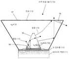
도 1은 테이퍼(taper)된 렌즈와 결합된 (Al, Ga, In)N과 ZnO 직접 웨이퍼 접합 LED 구조의 개략적인 단면도이며, 여기에서 상기 렌즈를 들어가는 대부분 의 빛은 임계각 내에 존재하여 추출된다.1 is a schematic cross-sectional view of a (Al, Ga, In) N and ZnO direct wafer bonded LED structure coupled with a tapered lens, where most of the light entering the lens is present within a critical angle and extracted.
도 2는 예를 들면 SiON, SiO2, ZnS, GaN, SiC 과 같은 임의의 고굴절율 물질 또는 고굴절율 고분자 또는 플라스틱 물질이 제2 광학 요소와 결합될 수 있는 더욱 일반적인 개념이다.FIG. 2 is a more general concept in which any high refractive index material such as SiON, SiO 2, ZnS, GaN, SiC or a high refractive index polymer or plastic material can be combined with a second optical element.
도 3(a) 및 3(b)는 테이퍼된 광학기(optics)와 결합된 ZnO 원뿔형 LED 를 도시한다.3 (a) and 3 (b) show ZnO conical LEDs combined with tapered optics.
도 4는 양쪽 면 위에 조형된 고굴절율 물질을 갖는 LED의 개략적인 단면도이다.4 is a schematic cross-sectional view of an LED having a high refractive index material molded on both sides.
도 5는 ZnO 원뿔형 웨이퍼 접합된 LED를 도시한다.5 shows a ZnO conical wafer bonded LED.
도 6은 2mA 순방향 전류 아래에서 ZnO 원뿔형 웨이퍼 접합된 LED를 도시한다.6 shows a ZnO conical wafer bonded LED under 2 mA forward current.
도 7은 조형된 플라스틱 광학 요소들과 결합된 조형된 고굴절율 추출기의 상면도이다.7 is a top view of a molded high refractive index extractor combined with molded plastic optical elements.
도 8은 양쪽 면 위에 있는 고굴절율 추출기와 구형(spherical) 플라스틱 광학 요소를 갖는 조형된 LED이다.8 is a modeled LED with a high refractive index extractor and spherical plastic optical elements on both sides.
도 9는 조형된 광학 요소와 결합된 소자의 양쪽 면에 ZnO 또는 (ITO와 같은) 투명한 전도체를 갖는 웨이퍼 접합된 LED의 개략적인 단면도이다.9 is a schematic cross-sectional view of a wafer bonded LED having ZnO or transparent conductors (such as ITO) on both sides of the device combined with the molded optical element.
도 10은 순방향에서 높은 광추출을 위한 테이퍼된 광학 디자인을 갖는 원뿔형 LED의 개략도이다.10 is a schematic diagram of a conical LED with a tapered optical design for high light extraction in the forward direction.
도 11은 높은 광추출 효율을 갖는 발광 다이오드(LED) 구조를 제조하기 위한 방법을 도시하는 흐름도이다.11 is a flow chart illustrating a method for manufacturing a light emitting diode (LED) structure having high light extraction efficiency.
다음의 바람직한 실시예의 기술에서 발명이 실시될 수 있는 특정 실시예를 도시한, 실시예의 일부를 구성하는 첨부된 도면을 참조하였다. 또한, 본 발명의 범위를 벗어나지 않으면서 다른 실시예들이 사용될 수 있고 구조적인 변화가 만들어질 수 있음이 이해되어야 할 것이다.Reference is made to the accompanying drawings, which form a part of the embodiments, illustrating specific embodiments in which the invention may be practiced in the following description of the preferred embodiments. It is also to be understood that other embodiments may be utilized and structural changes may be made without departing from the scope of the present invention.
개관survey
본 발명은 조형된 플라스틱 광학 구성요소와 결합된 (Al, Ga, In)N 와 ZnO 직접 웨이퍼 접합(direct wafer bonded) 발광 다이오드(LED)를 기술한다. 여기에서 LED 표면과 접촉하는 ZnO 콘(cone) 또는 임의의 고굴절율 물질로부터 조형된 플라스틱 광학 요소로 입사하는 방향성의 빛은 공기로 추출된다. 특히, (Al, Ga, In)N 와 ZnO 직접 웨이퍼 접합 발광 다이오드(LED) 구조는 테이퍼된(tapered) 렌즈와 결합되며, 이 렌즈를 입사하는 빛의 대부분은 임계각 안으로 들어와서 추출된다.The present invention describes (Al, Ga, In) N and ZnO direct wafer bonded light emitting diodes (LEDs) combined with molded plastic optical components. Here the directional light entering the molded plastic optical element from a ZnO cone or any high refractive index material in contact with the LED surface is extracted with air. In particular, the (Al, Ga, In) N and ZnO direct-wafer bonded light emitting diode (LED) structures are combined with tapered lenses, and most of the light entering the lens enters into the critical angle and is extracted.
본 발명은 콘의 수를 하나로 줄임으로써 이웃하는 콘들로부터의 흡수를 감소시킨다. 본 발명은 플라스틱 보호(encapsulant) 표면으로부터의 반사를 줄이고, ZnO 표면으로부터의 반사를 줄이고, LED 내부의 광흡수를 줄이고, 활성층으로부터의 균일한 발광을 가능하게 하고, LED 내부에서 반복적으로 일어나는 광반사를 줄인다. 결과로써 본 결합된 구조는 종래 기술에서 기술된 LED와 비교하여 LED로부터 더욱 많은 빛을 추출한다.The present invention reduces the absorption from neighboring cones by reducing the number of cones to one. The present invention reduces reflections from plastic encapsulant surfaces, reduces reflections from ZnO surfaces, reduces light absorption inside the LEDs, enables uniform light emission from the active layer, and light reflections that occur repeatedly within the LEDs. Reduce As a result, the combined structure extracts more light from the LED compared to the LEDs described in the prior art.
기술 설명Technical description
본 발명의 목적은 조형된 고굴절율 구성요소들을 (Al, Ga, In)N LED와 조형된 광학 요소들과 결합하여 LED로부터 광추출 효율을 증가시키는 수단을 제공하는 것이다. 광투과율과 광추출을 증가시킴으로써 결과적으로 소자 성능이 향상된다.It is an object of the present invention to provide a means of increasing the light extraction efficiency from LEDs by combining molded high refractive index components with (Al, Ga, In) N LEDs and molded optical elements. Increasing light transmittance and light extraction results in improved device performance.
본 발명의 일 실시예에서 고굴절율 ZnO 층은 GaN LED에 웨이퍼 접합(wafer bonded)된다. 고굴절율 ZnO 층 안에 콘이 식각되고, GaN LED 위에 콘택이 형성된다. ZnO/GaN 하이브리드 LED는 그후 약 45도 각도를 갖는 원뿔형의 플라스틱 렌즈 내에 놓여진다.In one embodiment of the invention, the high refractive index ZnO layer is wafer bonded to a GaN LED. The cone is etched in the high refractive index ZnO layer and a contact is formed over the GaN LED. The ZnO / GaN hybrid LED is then placed in a conical plastic lens with an angle of about 45 degrees.
도 1은 본 발명의 바람직한 실시예에 의한 높은 광추출 효율을 갖는 LED의 개략적인 모습을 보여준다. 일반적으로, LED는 (Al, Ga, In)N과 ZnO의 직접 웨이퍼 접합 LED 구조이다. 이 실시예에서 LED(10)는 사파이어 기판과 같은 기판(11) 위의 n-형 Ⅲ-질화물층(들), 활성층(들) 및 p-형 Ⅲ-질화물층(들)로 구성된다. 굴절율 n0=2.1 의 n-형 ZnO 콘(12)을 포함하는 제1 모양 광학 요소가 LED(10)의 상부 위에 놓여있다. LED와 n-ZnO 콘(12) 모두는 굴절율 ne=1.5 인 테이퍼된 또는 원뿔형 플라스틱 렌즈(13)를 포함하는 제2 광학 요소 안 또는 아래에 싸여지거나 커버된다.1 shows a schematic view of an LED having a high light extraction efficiency according to a preferred embodiment of the present invention. In general, LEDs are direct wafer bonded LED structures of (Al, Ga, In) N and ZnO. In this embodiment, the LED 10 consists of n-type III-nitride layer (s), active layer (s) and p-type III-nitride layer (s) on a substrate 11, such as a sapphire substrate. A first shaped optical element comprising an n-
콘(12)의 각(14) 및 원뿔형 플라스틱 렌즈(13)의 각(15)은 임계각(Θc)이고 원하는대로 조절될 수 있다. ZnO의 임계각 Θc(14)이 약 60도이면 대부분의 빛 이 탈출 원뿔(escape cone) 내에 있기 때문에 대부분의 빛은 제1 경로 위를 지난다 (즉, 대부분의 빛은 Θc 보다 작거나 같은 각도로 경계(16)에 부딪친다.)The
임계각(14), (15)은 제1 조형 광학 요소와 제2 조형 광학 요소 사이의 경계(16) 또는 제2 조형 광학 요소와 외부 매질(18) 사이의 경계(17)에서의 굴절율 비의 아크탄젠트(arctangent)에 의하여 주어진다. 여기서 굴절율비는 경계의 한 면에서의 굴절율을 경계의 다른 면에서의 굴절율로 나누어서 얻는다. 예를 들면, 공기/플라스틱 경계는 1/1.5의 비를 가지며 Θc=42도, 플라스틱/ZnO 경계는 1.5/2.1의 비를 가지며 Θc=46도, ZnO/GaN 경계는 2.1/2.3의 비를 가지며 Θc=66도 그리고 공기/ZnO 경계는 1/2.1의 비를 가지며 Θc=28도이다. 도 1에서 화살표(19)는 LED(10)에 의해 콘(12)으로 방출되고 공기로 추출되는 빛의 가능한 경로를 지시한다.The
LED(10)로부터 제1 조형 광학 요소(12)로 들어가는 빛이 하나 또는 그 이상의 제2 조형 광학 요소들의 경계(16)에서 하나 또는 그 이상의 제2 조형 광학 요소들로의 굴절을 위한 임계각 내로 들어가도록 제1 조형 광학 요소 (12)는 임계각(14)을 갖는 형태로 만들어 진다. 제1 및 제2 조형 광학 요소들을 통하여 투과하는, LED로부터 나온 대부분의 빛이 하나 또는 그 이상의 제2 조형 광학 요소들(13)로부터의 굴절을 위한 임계각 내에서 (예를 들면, 공기와 같은) 외부 매질(18)의 경계(17)에 부딪치도록 하기 위하여 제2 조형 광학 요소(13)는 임계각 (15)를 갖는 형태로 만들어 진다.Light entering the first modeling
도 2는 본 발명의 바람직한 실시예에 의한 높은 광추출 효율을 갖는 LED 의 개략적인 모습을 보여준다. 도 2는 LED의 굴절율 nled, 콘의 굴절율 n0 및 렌즈의 굴절율 ne의 바람직한 관계를 보여준다. 더욱 특정하게는, 도 2는 (Al, Ga, In)N-계 LED(20), (Al, Ga, In)N-계 LED(20)에 인접하거나 (Al, Ga, In)N-계 LED(20)의 표면 위에 있거나 (Al, Ga, In)N-계 LED(20)를 둘러싸는 고굴절율 물질로 구성된 제1 "조형" 광학 요소(21) (예를 들면 콘), (Al, Ga, In)N-계 LED(20)와 제1 조형 광학 요소(21) 모두를 에워싸거나 커버하는 낮은 굴절율 물질로 구성된 제2 "조형" 광학 요소(22) (예를 들면 렌즈)의 결합에 의하여 높은 광추출 효율을 제공하는 본 발명의 개념을 도시한다. 일반적으로, 고굴절율 물질의 굴절율 n0은 낮은 굴절율 물질의 굴절율 ne 보다 크다. 즉, n0 > ne이다. 도 2의 화살표는 LED(20)에 의해 방출된 빛의 가능한 경로를 보여준다.Figure 2 shows a schematic view of the LED having a high light extraction efficiency according to a preferred embodiment of the present invention. Figure 2 shows the preferred relationship between the refractive index nled of the LED, the refractive index n0 of the cone and the refractive index ne of the lens. More specifically, FIG. 2 is adjacent to (Al, Ga, In) N-based
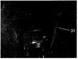
도 3(a) 및 3(b)는 순방향 전압 아래에서 밝은 청색광을 방출하는, 본 발명의 바람직한 실시예에 따라 ZnO 콘을 포함하는 구성된 제1 조형 광학 요소와 테이퍼된 렌즈(31)를 포함하는 제2 조형 광학 요소를 갖는 LED를 보여주는 사진들이다.3 (a) and 3 (b) comprise a tapered
테이퍼된 원뿔형 플라스틱 렌즈 LED와 결합된 원뿔형 LED는 20mA 구동 전류에서 460nm 발광 파장에 대하여 22mW의 출력을 갖는 것으로 관측되었다. 이것은 동일한 에피택셜 웨이퍼로부터 제조된 일반적인 GaN 칩에 대하여 약 500%의 광출력의 증가를 증명한다.Conical LEDs combined with tapered conical plastic lens LEDs were observed to have an output of 22 mW for a 460 nm emission wavelength at 20 mA drive current. This demonstrates an increase in light output of about 500% for a typical GaN chip made from the same epitaxial wafer.
도 4는 LED(40)의 양쪽 면 위의 그리고 LED(40)를 둘러싼 고굴절율 물질 로된 제1 조형 광학 요소(41)와 테이퍼된 렌즈(42)를 갖는 LED(40)의 구체적인 실시예를 도시한다. 도 4의 화살표는 LED(40)에 의해 방출된 빛의 가능한 경로를 보여준다.4 illustrates a specific embodiment of an
도 5는 전기적인 콘택(50)을 갖는 ZnO 원뿔 형태의 웨이퍼 접합 LED를 보여주는 사진이다.5 is a photograph showing a wafer bonded LED in the form of a ZnO cone with an
도 6은 2mA 아래의 순방향 전류가 전기적인 콘택(61) 및 와이어(62)를 통하여 흐르는 동안, 청색광을 방출하는 ZnO 원뿔 형태의 웨이퍼 접합 LED를 보여주는 사진이다.6 is a photograph showing a wafer bonded LED in the form of a ZnO cone that emits blue light while a forward current below 2 mA flows through
도 7은 제1 및 제2 조형 광학 요소들로 사용될 수 있는 다양한 조합과 구조들을 도시한다. 광학 요소들은 그들 각각의 높고 낮은 굴절율에 의하여 확인된다. 화살표들은 제1 조형 광학 요소에 둘러싸인 LED에 의해 방출된 빛의 가능한 경로를 보여준다. 고굴절율 물질을 포함하는 제1 조형 광학 요소는 LED에 의해 방출되는 빛을 추출하기 위한 것이고, 낮은 굴절율을 포함하는 제2 조형 광학 요소는 LED와 제1 조형 광학 요소에 의해 방출되는 빛을 추출하기 위한 것이다.7 illustrates various combinations and structures that can be used as the first and second modeling optical elements. Optical elements are identified by their high and low refractive indices. The arrows show the possible paths of light emitted by the LED surrounded by the first modeling optical element. The first modeling optical element comprising a high refractive index material is for extracting light emitted by the LED, and the second modeling optical element comprising a low refractive index is for extracting light emitted by the LED and the first modeling optical element. It is for.
도 8은 본 발명의 구체적인 실시예에 의한 높은 광추출 효율을 갖는 LED의 개략적인 모습을 보여준다. LED는 n-형 Ⅲ-질화물층(80), 활성층(81) 및 p-형 Ⅲ-질화물층(82)로 구성된다. n-형 Ⅲ-질화물층(80)에 인접하여 전극(83)과 제1 ZnO 콘 형태의 요소(84)가 있다. 제1 ZnO 콘(84)의 상부 위에 n-형 전극(85)가 있다. p-형 Ⅲ-질화물층(82)에 인접하여 제2 n-형 ZnO 콘 형태의 요소(86)이 있고, ZnO 콘(86)의 상부 위에 p-형 전극(87)이 있다. 그러므로 LED는 양쪽 면들 위에 고 굴절율 광추출기들 (예를 들면, 제1(84) 및 제2(86) ZnO 콘-형태의 요소들)을 구성하는 제1 조형 광학 요소들을 포함한다. 바깥쪽 원(88)은 렌즈를 포함하는 제2 조형 광학 요소를 나타낸다. 화살표들(89)은 LED의 활성 영역(81)으로부터 방출된 빛의 가능한 경로를 보여준다.8 shows a schematic view of an LED having a high light extraction efficiency according to a specific embodiment of the present invention. The LED is composed of an n-type III-nitride layer 80, an active layer 81, and a p-type III-nitride layer 82. Adjacent to n-type III-nitride layer 80 is
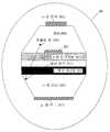
도 9는 본 발명의 구체적인 실시예에 의한 높은 광추출 효율을 갖는 LED의 개략적인 모습을 보여준다. LED는 SiC 또는 GaN 기판(90), n-형 Ⅲ-질화물층(91), 활성 영역(92) 및 p-형 Ⅲ-질화물층(93)으로 구성된다. p-형 Ⅲ-질화물층(83)에 인접하여 n-형 ZnO 층(94)가 있고, ZnO(94)의 상부 위에 p-형 전극(95)가 있다. 기판(90)에 인접하여 ZnO 콘 형태 요소(96)이 있고, ZnO(96) 위에 n-형 전극(97)이 있다. 바깥쪽 삼각형(98)은 렌즈를 나타내고, 화살표들(99)은 LED로부터 방출된 빛의 가능한 경로를 보여준다.9 shows a schematic view of an LED having a high light extraction efficiency according to a specific embodiment of the present invention. The LED is composed of a SiC or GaN substrate 90, an n-type III-nitride layer 91, an active region 92 and a p-type III-nitride layer 93. Adjacent to the p-type III-
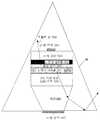
도 10은 본 발명의 구체적인 실시예에 의한 높은 광추출 효율을 갖는 LED의 개략적인 모습을 보여준다. LED는 n-형 Ⅲ-질화물층(100), 활성 영역(101) 및 p-형 Ⅲ-질화물층(102)를 포함한다. n-형 Ⅲ-질화물층(100)에 인접하여 n-형 전극(103)이 있다. p-형 Ⅲ-질화물층(102)에 인접하여 잘린 육각 피라미드(truncated hexagonal pyramid)를 포함하는 n-형 ZnO 콘-형태의 요소(104)가 있고, ZnO(104)의 상부 위에 p-형 전극(105)가 있다. 바깥쪽 사다리꼴(106)은 플라스틱 렌즈들을 나타내고, 렌즈들은 고반사 코팅(107)을 가질 수 있다. ZnO 콘(104)은 예를 들면, {10-11} 평면의 표면(108)을 갖는 잘린 육각 피라미드일 수 있다. 화살표들(109)은 LED로부터 방출된 빛의 가능한 경로를 보여준다.Figure 10 shows a schematic view of the LED having a high light extraction efficiency according to a specific embodiment of the present invention. The LED includes an n-type III-nitride layer 100, an
도 11은 높은 광추출 효율을 갖는 발광 다이오드(LED) 구조를 제조하는 방법을 나타낸다.11 shows a method of manufacturing a light emitting diode (LED) structure having high light extraction efficiency.
블록 110은 웨이퍼 접합된 구조를 형성하기 위하여 LED에 투명한 도전체를 포함하는 제1 광학 요소를 웨이퍼 접합하는 단계를 나타낸다.
블록 111은 제2 광학 요소로의 빛의 굴절을 최대화하기 위하여 제1 광학 요소를 조형하는 단계를 나타낸다.
블록 112는 웨이퍼 접합된 구조를 제2 광학 요소로 둘러싸거나 커버하는 단계를 나타낸다. 여기에서 제2 광학 요소는 제1 광학 요소의 굴절율보다 낮은 굴절율을 가지며, 제2 광학 요소로부터 빛의 굴절을 최대화하도록 조형된다.
가능한 변경Possible changes
본 발명의 장점은 조형된 표면으로부터 방출하는 빛을 추출하기 위하여 디자인된 광학기들(optics)과 조합된 (Al, Ga, In)N과 ZnO LED 구조의 본딩 및 조형으로부터 도출된다. 이 조합은 새로운 것이며, 특히 LED 응용을 위하여 기존의 소자 디자인들에 대하여 장점을 갖는다.The advantages of the present invention are derived from the bonding and shaping of the (Al, Ga, In) N and ZnO LED structures combined with optics designed to extract light emitted from the shaped surface. This combination is new and has advantages over existing device designs, especially for LED applications.
Ⅲ-질화물 LED는 예를 들면, (Al, Ga, In)N 물질들, (Al, Ga, In)As 물질들, (Al, Ga, In)P 물질들, (Al, Ga, In)AsPNSb 물질들로부터 만들어진 화합물 반도체 물질 또는 ZnGeN2 or ZnSnGeN2 물질들로부터 만들어진 화합물 반도체 물질로 구성될 수 있다.III-nitride LEDs are for example (Al, Ga, In) N materials, (Al, Ga, In) As materials, (Al, Ga, In) P materials, (Al, Ga, In) AsPNSb It may be composed of a compound semiconductor material made from materials or a compound semiconductor material made from ZnGeN2 or ZnSnGeN2 materials.
(Al, Ga, In)N 물질들에 관련하여, LED는 극성(polar) c-면 {0001} (Al, Ga, In)N, a-면 {11-20}, 비극성 m-면 {1-100} (Al, Ga, In)N 또는 준극성(semipolar) (Al, Ga, In)N으로 구성될 수 있다. 여기에서 준극성은 두 개의 0이 아닌h,i, 또는k 밀러 지수(Miller indices)와 하나의 0이 아닌 / 밀러 지수, {hikl} 를 갖는 매우 다양한 평면들을 지칭한다.With respect to (Al, Ga, In) N materials, the LEDs have a polar c-plane {0001} (Al, Ga, In) N, a-plane {11-20}, nonpolar m-plane {1 -100} (Al, Ga, In) N or semipolar (Al, Ga, In) N. Quasi-polarity here refers to a wide variety of planes with two nonzeroh ,i , ork Miller indices and one nonzero / miller index, {hikl }.
덧붙여, LED는 예를 들면, 사파이어, 실리콘 카바이드, 실리콘, 저마늄, 갈륨 아세나이드(gallium arsenide), 갈륨 포스파이드(gallium phosphide), 인듐 포스파이드(indium phosphide) 또는 스피넬 웨이퍼(spinel wafer) 위에 또는 갈륨 질화물(gallium nitride) 위에 또는 다른 기판들로부터 제거된 자립형(free-standing) 갈륨 질화물 위에 성장될 수 있다.In addition, the LEDs may be, for example, on sapphire, silicon carbide, silicon, germanium, gallium arsenide, gallium phosphide, indium phosphide or spinel wafers or It can be grown on gallium nitride or on free-standing gallium nitride removed from other substrates.
고굴절율 물질들은 많은 다양한 물질들, 예를 들면, ZnO, GaN, SiC, SiON, SiN, SiO2, 고굴절율 금속 산화물, 고굴절율 고분자 또는 고굴절율 플라스틱 물질로 구성될 수 있다. 낮은 굴절율 물질들은 또한 많은 다양한 유형의 물질들, 예를 들면, 플라스틱으로 구성될 수 있다. 이러한 물질들은 임의의 수의 다양한 방법들을 사용하여 표면을 거칠게 처리하거나(roughened) 조형할 수 있다.High refractive index materials can be composed of many different materials, such as ZnO, GaN, SiC, SiON, SiN, SiO2, high refractive index metal oxides, high refractive index polymers or high refractive index plastic materials. Low refractive index materials may also consist of many different types of materials, for example plastics. Such materials can be roughened or shaped using any number of various methods.
일반적으로, 제1 조형 광학 요소는 60%가 넘는 투과도와 LED와 오믹 콘택을 만들기에 충분한 전기적인 전도성을 갖도록 선택된 임의의 고굴절율 물질을 포함할 수 있다. 본 명세서를 통하여 사용되는 ZnO는 임의의 도핑된 반도체층에 인접한 n 형, p 형 또는 비도핑된 것일 수 있다. (즉, p-형 반도체 또는 n-형 반도체에 인접한 n-형 ZnO 또는 p-형 또는 n-형 반도체에 인접한 p-형 ZnO)In general, the first modeling optical element may include any high refractive index material selected to have a transmittance of greater than 60% and sufficient electrical conductivity to make the ohmic contact with the LED. As used herein, ZnO may be n-type, p-type or undoped adjacent to any doped semiconductor layer. (Ie, n-type ZnO adjacent to a p-type semiconductor or n-type semiconductor or p-type ZnO adjacent to a p-type or n-type semiconductor)
위에서 주목된 바와 같이, 일 실시예에서 LED는 (Al, Ga, In)N 층들로 구성되며, 고굴절율 광추출 물질은 (Al, Ga, In)N 층들에 웨이퍼 접합된 ZnO 층들로 구성된다. 조형된 또는 표면이 거칠게 처리된 ZnO은 LED 내에서 반복적으로 일어나는 광반사들을 줄이고, 그리하여 LED로부터 더 많은 빛을 추출한다. ZnO의 (60% 이상의) 매우 투명한 특성은 LED 내부의 광흡수를 줄인다. ZnO의 전기적인 전도성 특성은 LED에서 활성 영역으로부터 균일한 발광을 가능하게 한다. 이 새로운 하이브리드 GaN/ZnO/조형 렌즈 디자인의 결과적인 외부 양자 효율(external quantum efficiency)은 기존의 GaN-계 LED 소자들보다 더 높을 것이다.As noted above, in one embodiment the LED is comprised of (Al, Ga, In) N layers and the high refractive index light extraction material is comprised of ZnO layers wafer bonded to the (Al, Ga, In) N layers. Molded or roughened ZnO reduces light reflections that occur repeatedly in the LED, thus extracting more light from the LED. The highly transparent (more than 60%) nature of ZnO reduces light absorption inside the LEDs. The electrically conductive properties of ZnO allow uniform light emission from the active region in the LED. The resulting external quantum efficiency of this new hybrid GaN / ZnO / fabricated lens design will be higher than that of conventional GaN-based LED devices.
ZnO는 LED 방출에 더하여 청색, 황색, 적색 및 백색광과 같은 다른 색을 방출하도록 도핑될 수 있다.ZnO can be doped to emit other colors such as blue, yellow, red and white light in addition to LED emission.
더욱이, SiC 또는 GaN과 같은 전기적으로 전도성의 기판 위에 성장된 질화물 LED와 투명한 ZnO 전극의 조합은 LED의 제조에 요구되는 공정 단계들의 수를 줄일 수 있는데, 이것은 전극이 전기적으로 전도성의 물질 위에 쉽게 형성될 수 있기 때문이다. 그러나 다른 실시예들에서, ZnO는 반드시 웨이퍼 접합될 필요는 없고, 대신에 매우 다양한 수단에 의하여 증착될 수 있다.Moreover, the combination of a nitride LED and a transparent ZnO electrode grown on an electrically conductive substrate such as SiC or GaN can reduce the number of process steps required for the manufacture of the LED, which makes the electrode easily formed on the electrically conductive material. Because it can be. However, in other embodiments, ZnO does not necessarily need to be wafer bonded, but instead may be deposited by a wide variety of means.
마지막으로, 콘이나 다른 형태의 광학 요소들의 수에 관련하여 더 적은 수가 더 좋다. 각각의 콘은 이웃의 콘으로부터 발광을 흡수할 수 있기 때문이다. 오직 하나의 콘이 있을 때, 다른 콘들이 없으므로 다른 이웃 콘으로부터의 흡수와 같은 영향이 없다. 다중-콘 LED에 관한 추가 정보를 [7]에서 찾을 수 있다.Finally, fewer numbers are better with respect to the number of cones or other types of optical elements. This is because each cone can absorb light emission from a neighboring cone. When there is only one cone, there are no other cones, so there is no effect as absorption from other neighboring cones. Additional information on multi-cone LEDs can be found in [7].
본 발명의 장점은 표준 사각 GaN 칩과 비교하여 광추출 효율을 굉장히 증가시킨다는 것이다. 아래의 표 1은 본 발명으로 제조된 동일한 에피택셜 물질이 20mA 구동 전류 아래에 460nm 파장에서 15-22mW의 발광을 낳는 것을 보여준다. 이것은 표준 사각 칩의 20mA에서 4-5mW의 파워에 대하여 약 500%의 증가이다.The advantage of the present invention is that it greatly increases the light extraction efficiency compared to standard square GaN chips. Table 1 below shows that the same epitaxial material produced with the present invention produces 15-22mW emission at 460nm wavelength under 20mA drive current. This is an increase of about 500% for a power of 4-5mW at 20mA of a standard square chip.
표 1Table 1
참조Reference
다음의 문헌들이 참조에 의하여 여기에 통합될 것이다.The following documents will be incorporated herein by reference.
[1] Appl. Phys. Lett. 56, 737-39 (1990).[2] Appl. Phys. Lett. 64, 2839-41 (1994).[3] Appl. Phys. Lett. 81, 3152-54 (2002).[1] Appl. Phys. Lett. 56, 737-39 (1990). [2] Appl. Phys. Lett. 64, 2839-41 (1994). Appl. Phys. Lett. 81, 3152-54 (2002).
[4] Jpn. J. Appl. Phys. 43, L1275-77 (2004).[4] Jpn. J. Appl. Phys. 43, L1275-77 (2004).
[5] J. J. Appl. Phys. 34, L797-99 (1995).[5] J. J. Appl. Phys. 34, L797-99 (1995).
[6] J. J. Appl. Phys. 43, L180-82 (2004)[6] J. J. Appl. Phys. 43, L180-82 (2004)
[7] Appl. Phys. Lett. 84, 855 (2004).[7] Appl. Phys. Lett. 84, 855 (2004).
결론conclusion
이것으로 본 발명의 바람직한 실시예의 기술을 마친다. 본 발명의 하나 또는 그 이상의 실시예들의 앞의 기술은 도해와 설명의 목적으로 제공되었다. 이것은 한정적이거나 본 발명을 기술된 정확한 형태로 제한하는 것으로 의도되지 않는다. 많은 변용들과 변화들이 위의 교시에 비추어 가능하다. 발명의 범위가 이 상세한 설명에 의해서가 아니라 오히려 부가된 청구항들에 의하여 제한되는 것으로 의도된다.This concludes the description of the preferred embodiment of the present invention. The foregoing description of one or more embodiments of the invention has been presented for purposes of illustration and description. It is not intended to be exhaustive or to limit the invention to the precise form described. Many variations and changes are possible in light of the above teachings. It is intended that the scope of the invention be limited not by this detailed description, but rather by the appended claims.
Claims (20)
Translated fromKoreanApplications Claiming Priority (2)
| Application Number | Priority Date | Filing Date | Title |
|---|---|---|---|
| US73404005P | 2005-11-04 | 2005-11-04 | |
| US60/734,040 | 2005-11-04 |
Publications (1)
| Publication Number | Publication Date |
|---|---|
| KR20080074948Atrue KR20080074948A (en) | 2008-08-13 |
Family
ID=38023921
Family Applications (1)
| Application Number | Title | Priority Date | Filing Date |
|---|---|---|---|
| KR1020087013442ACeasedKR20080074948A (en) | 2005-11-04 | 2006-11-06 | Light emitting diode with high light extraction efficiency |
Country Status (6)
| Country | Link |
|---|---|
| US (1) | US7994527B2 (en) |
| EP (1) | EP1949463A4 (en) |
| JP (1) | JP2009515344A (en) |
| KR (1) | KR20080074948A (en) |
| TW (1) | TW200733424A (en) |
| WO (1) | WO2007056354A2 (en) |
Cited By (1)
| Publication number | Priority date | Publication date | Assignee | Title |
|---|---|---|---|---|
| KR101147322B1 (en)* | 2009-09-29 | 2012-05-18 | 산켄덴키 가부시키가이샤 | Light emitting semiconductor device, light emitting semiconductor module and lighting device |
Families Citing this family (90)
| Publication number | Priority date | Publication date | Assignee | Title |
|---|---|---|---|---|
| US20060005763A1 (en)* | 2001-12-24 | 2006-01-12 | Crystal Is, Inc. | Method and apparatus for producing large, single-crystals of aluminum nitride |
| US8545629B2 (en) | 2001-12-24 | 2013-10-01 | Crystal Is, Inc. | Method and apparatus for producing large, single-crystals of aluminum nitride |
| US7638346B2 (en)* | 2001-12-24 | 2009-12-29 | Crystal Is, Inc. | Nitride semiconductor heterostructures and related methods |
| US7842527B2 (en) | 2006-12-11 | 2010-11-30 | The Regents Of The University Of California | Metalorganic chemical vapor deposition (MOCVD) growth of high performance non-polar III-nitride optical devices |
| US9130119B2 (en)* | 2006-12-11 | 2015-09-08 | The Regents Of The University Of California | Non-polar and semi-polar light emitting devices |
| US7345298B2 (en)* | 2005-02-28 | 2008-03-18 | The Regents Of The University Of California | Horizontal emitting, vertical emitting, beam shaped, distributed feedback (DFB) lasers by growth over a patterned substrate |
| US8324660B2 (en) | 2005-05-17 | 2012-12-04 | Taiwan Semiconductor Manufacturing Company, Ltd. | Lattice-mismatched semiconductor structures with reduced dislocation defect densities and related methods for device fabrication |
| US9153645B2 (en) | 2005-05-17 | 2015-10-06 | Taiwan Semiconductor Manufacturing Company, Ltd. | Lattice-mismatched semiconductor structures with reduced dislocation defect densities and related methods for device fabrication |
| EP1908125A2 (en)* | 2005-06-17 | 2008-04-09 | The Regents of the University of California | (AI,Ga,In)N AND ZnO DIRECT WAFER BONDED STRUCTURE FOR OPTOELECTRONIC APPLICATION AND ITS FABRICATION METHOD |
| US8148713B2 (en)* | 2008-04-04 | 2012-04-03 | The Regents Of The University Of California | Method for fabrication of semipolar (Al, In, Ga, B)N based light emitting diodes |
| WO2007065005A2 (en)* | 2005-12-02 | 2007-06-07 | The Regents Of University Of California | Improved horizontal emitting, vertical emitting, beam shaped, distributed feedback (dfb) lasers fabricated by growth over a patterned substrate with multiple overgrowth |
| JP5281408B2 (en) | 2005-12-02 | 2013-09-04 | クリスタル・イズ,インコーポレイテッド | Doped aluminum nitride crystal and method for producing the same |
| KR20080077259A (en)* | 2005-12-08 | 2008-08-21 | 더 리전츠 오브 더 유니버시티 오브 캘리포니아 | High efficiency light emitting diode |
| WO2007112066A2 (en) | 2006-03-24 | 2007-10-04 | Amberwave Systems Corporation | Lattice-mismatched semiconductor structures and related methods for device fabrication |
| US9034103B2 (en)* | 2006-03-30 | 2015-05-19 | Crystal Is, Inc. | Aluminum nitride bulk crystals having high transparency to ultraviolet light and methods of forming them |
| US8012257B2 (en)* | 2006-03-30 | 2011-09-06 | Crystal Is, Inc. | Methods for controllable doping of aluminum nitride bulk crystals |
| US20070284565A1 (en)* | 2006-06-12 | 2007-12-13 | 3M Innovative Properties Company | Led device with re-emitting semiconductor construction and optical element |
| US8173551B2 (en) | 2006-09-07 | 2012-05-08 | Taiwan Semiconductor Manufacturing Co., Ltd. | Defect reduction using aspect ratio trapping |
| WO2008039534A2 (en) | 2006-09-27 | 2008-04-03 | Amberwave Systems Corporation | Quantum tunneling devices and circuits with lattice- mismatched semiconductor structures |
| WO2008045423A1 (en)* | 2006-10-10 | 2008-04-17 | Structured Materials Inc. | Self assembled controlled luminescent transparent conductive photonic crystals for light emitting devices |
| US8502263B2 (en) | 2006-10-19 | 2013-08-06 | Taiwan Semiconductor Manufacturing Company, Ltd. | Light-emitter-based devices with lattice-mismatched semiconductor structures |
| US20090121250A1 (en)* | 2006-11-15 | 2009-05-14 | Denbaars Steven P | High light extraction efficiency light emitting diode (led) using glass packaging |
| WO2008060584A2 (en)* | 2006-11-15 | 2008-05-22 | The Regents Of The University Of California | High light extraction efficiency sphere led |
| WO2008060615A1 (en)* | 2006-11-15 | 2008-05-22 | The Regents Of The University Of California | Transparent mirrorless light emitting diode |
| WO2008060586A2 (en) | 2006-11-15 | 2008-05-22 | The Regents Of The University Of California | Textured phosphor conversion layer light emitting diode |
| JP2010512662A (en) | 2006-12-11 | 2010-04-22 | ザ リージェンツ オブ ザ ユニバーシティ オブ カリフォルニア | Transparent light emitting diode |
| US8323406B2 (en)* | 2007-01-17 | 2012-12-04 | Crystal Is, Inc. | Defect reduction in seeded aluminum nitride crystal growth |
| US9771666B2 (en) | 2007-01-17 | 2017-09-26 | Crystal Is, Inc. | Defect reduction in seeded aluminum nitride crystal growth |
| WO2008094464A2 (en)* | 2007-01-26 | 2008-08-07 | Crystal Is, Inc. | Thick pseudomorphic nitride epitaxial layers |
| US8080833B2 (en) | 2007-01-26 | 2011-12-20 | Crystal Is, Inc. | Thick pseudomorphic nitride epitaxial layers |
| US7825328B2 (en) | 2007-04-09 | 2010-11-02 | Taiwan Semiconductor Manufacturing Company, Ltd. | Nitride-based multi-junction solar cell modules and methods for making the same |
| US8237151B2 (en) | 2009-01-09 | 2012-08-07 | Taiwan Semiconductor Manufacturing Company, Ltd. | Diode-based devices and methods for making the same |
| WO2008124154A2 (en) | 2007-04-09 | 2008-10-16 | Amberwave Systems Corporation | Photovoltaics on silicon |
| US8304805B2 (en) | 2009-01-09 | 2012-11-06 | Taiwan Semiconductor Manufacturing Company, Ltd. | Semiconductor diodes fabricated by aspect ratio trapping with coalesced films |
| US8088220B2 (en) | 2007-05-24 | 2012-01-03 | Crystal Is, Inc. | Deep-eutectic melt growth of nitride crystals |
| US8329541B2 (en) | 2007-06-15 | 2012-12-11 | Taiwan Semiconductor Manufacturing Company, Ltd. | InP-based transistor fabrication |
| KR20100059820A (en) | 2007-07-26 | 2010-06-04 | 더 리전츠 오브 더 유니버시티 오브 캘리포니아 | Light emitting diodes with a p-type surface |
| JP2010538495A (en) | 2007-09-07 | 2010-12-09 | アンバーウェーブ・システムズ・コーポレーション | Multi-junction solar cell |
| TW200950162A (en) | 2008-04-04 | 2009-12-01 | Univ California | Method for fabrication of semipolar (Al, In, Ga, B)N based light emitting diodes |
| JP2011517099A (en)* | 2008-04-04 | 2011-05-26 | ザ リージェンツ オブ ザ ユニバーシティ オブ カリフォルニア | MOCVD growth technology for planar semipolar (Al, In, Ga, B) N-based light-emitting diodes |
| US8183667B2 (en) | 2008-06-03 | 2012-05-22 | Taiwan Semiconductor Manufacturing Co., Ltd. | Epitaxial growth of crystalline material |
| US8274097B2 (en) | 2008-07-01 | 2012-09-25 | Taiwan Semiconductor Manufacturing Company, Ltd. | Reduction of edge effects from aspect ratio trapping |
| US8981427B2 (en) | 2008-07-15 | 2015-03-17 | Taiwan Semiconductor Manufacturing Company, Ltd. | Polishing of small composite semiconductor materials |
| US20100072515A1 (en) | 2008-09-19 | 2010-03-25 | Amberwave Systems Corporation | Fabrication and structures of crystalline material |
| EP2335273A4 (en) | 2008-09-19 | 2012-01-25 | Taiwan Semiconductor Mfg | FORMATION OF DEVICES BY GROWTH OF EPITAXIAL LAYERS |
| US8253211B2 (en) | 2008-09-24 | 2012-08-28 | Taiwan Semiconductor Manufacturing Company, Ltd. | Semiconductor sensor structures with reduced dislocation defect densities |
| CN102171846A (en)* | 2008-10-09 | 2011-08-31 | 加利福尼亚大学董事会 | Photoelectrochemical etching for chip shaping of light-emitting diodes |
| JP2010147446A (en) | 2008-12-22 | 2010-07-01 | Panasonic Electric Works Co Ltd | Light-emitting device |
| US8629446B2 (en) | 2009-04-02 | 2014-01-14 | Taiwan Semiconductor Manufacturing Company, Ltd. | Devices formed from a non-polar plane of a crystalline material and method of making the same |
| US8389388B2 (en) | 2009-04-30 | 2013-03-05 | Hewlett-Packard Development Company, L.P. | Photonic device and method of making the same |
| CN102460747B (en)* | 2009-06-04 | 2015-04-15 | 皇家飞利浦电子股份有限公司 | Efficient light emitting device and method for manufacturing such device |
| US20100314551A1 (en)* | 2009-06-11 | 2010-12-16 | Bettles Timothy J | In-line Fluid Treatment by UV Radiation |
| WO2011056867A1 (en)* | 2009-11-03 | 2011-05-12 | The Regents Of The University Of California | High brightness light emitting diode covered by zinc oxide layers on multiple surfaces grown in low temperature aqueous solution |
| KR101007145B1 (en)* | 2010-01-14 | 2011-01-10 | 엘지이노텍 주식회사 | Method of manufacturing light emitting device chip, light emitting device package and light emitting device chip |
| KR101064036B1 (en)* | 2010-06-01 | 2011-09-08 | 엘지이노텍 주식회사 | Light emitting device package and lighting system |
| CN105951177B (en) | 2010-06-30 | 2018-11-02 | 晶体公司 | Use the growth for the bulk aluminum nitride single crystal that thermal gradient controls |
| US20120153297A1 (en)* | 2010-07-30 | 2012-06-21 | The Regents Of The University Of California | Ohmic cathode electrode on the backside of nonpolar m-plane (1-100) and semipolar (20-21) bulk gallium nitride substrates |
| US10147853B2 (en) | 2011-03-18 | 2018-12-04 | Cree, Inc. | Encapsulant with index matched thixotropic agent |
| WO2013005147A1 (en) | 2011-07-01 | 2013-01-10 | Koninklijke Philips Electronics N.V. | Light guide |
| US8962359B2 (en) | 2011-07-19 | 2015-02-24 | Crystal Is, Inc. | Photon extraction from nitride ultraviolet light-emitting devices |
| TWI441362B (en)* | 2011-10-05 | 2014-06-11 | Delta Electronics Inc | Light-emitting module and light-emitting device thereof |
| GB201202222D0 (en) | 2012-02-09 | 2012-03-28 | Mled Ltd | Enhanced light extraction |
| JP2013197309A (en)* | 2012-03-19 | 2013-09-30 | Toshiba Corp | Light-emitting device |
| JP5756054B2 (en)* | 2012-04-16 | 2015-07-29 | 信越化学工業株式会社 | Thermosetting resin composition for LED reflector, LED reflector and optical semiconductor device using the same |
| US10424702B2 (en) | 2012-06-11 | 2019-09-24 | Cree, Inc. | Compact LED package with reflectivity layer |
| US20130328074A1 (en)* | 2012-06-11 | 2013-12-12 | Cree, Inc. | Led package with multiple element light source and encapsulant having planar surfaces |
| US10468565B2 (en) | 2012-06-11 | 2019-11-05 | Cree, Inc. | LED package with multiple element light source and encapsulant having curved and/or planar surfaces |
| US9818919B2 (en) | 2012-06-11 | 2017-11-14 | Cree, Inc. | LED package with multiple element light source and encapsulant having planar surfaces |
| US9887327B2 (en) | 2012-06-11 | 2018-02-06 | Cree, Inc. | LED package with encapsulant having curved and planar surfaces |
| US9046242B2 (en) | 2012-08-10 | 2015-06-02 | Groupe Ledel Inc. | Light dispersion device |
| US8796693B2 (en)* | 2012-12-26 | 2014-08-05 | Seoul Semiconductor Co., Ltd. | Successive ionic layer adsorption and reaction process for depositing epitaxial ZnO on III-nitride-based light emitting diode and light emitting diode including epitaxial ZnO |
| US20150280057A1 (en) | 2013-03-15 | 2015-10-01 | James R. Grandusky | Methods of forming planar contacts to pseudomorphic electronic and optoelectronic devices |
| FR3005785B1 (en)* | 2013-05-14 | 2016-11-25 | Aledia | OPTOELECTRONIC DEVICE AND METHOD FOR MANUFACTURING THE SAME |
| FR3005784B1 (en) | 2013-05-14 | 2016-10-07 | Aledia | OPTOELECTRONIC DEVICE AND METHOD FOR MANUFACTURING THE SAME |
| CN105393372B (en)* | 2013-07-26 | 2018-06-15 | 亮锐控股有限公司 | LED dome with internal high-refractive-index columns |
| JP2015207752A (en)* | 2014-04-08 | 2015-11-19 | パナソニックIpマネジメント株式会社 | Nitride semiconductor light emitting diode |
| JP6156402B2 (en) | 2015-02-13 | 2017-07-05 | 日亜化学工業株式会社 | Light emitting device |
| WO2018200417A1 (en) | 2017-04-24 | 2018-11-01 | Pcms Holdings, Inc. | Systems and methods for 3d displays with flexible optical layers |
| WO2019040484A1 (en) | 2017-08-23 | 2019-02-28 | Pcms Holdings, Inc. | Light field image engine method and apparatus for generating projected 3d light fields |
| EP3704531B1 (en) | 2017-11-02 | 2023-12-06 | InterDigital Madison Patent Holdings, SAS | Method and system for aperture expansion in light field displays |
| EP3794404B1 (en) | 2018-05-17 | 2023-07-26 | InterDigital Madison Patent Holdings, SAS | 3d display directional backlight based on diffractive elements |
| KR102620159B1 (en) | 2018-10-08 | 2024-01-02 | 삼성전자주식회사 | Semiconductor light emitting device |
| CN113557463B (en) | 2019-03-08 | 2024-08-20 | Pcms控股公司 | Optical method and system for displays based on light beams with extended depth of focus |
| EP3953748A1 (en) | 2019-04-12 | 2022-02-16 | PCMS Holdings, Inc. | Optical method and system for light field displays having light-steering layers and periodic optical layer |
| US11991343B2 (en) | 2019-06-07 | 2024-05-21 | Interdigital Madison Patent Holdings, Sas | Optical method and system for light field displays based on distributed apertures |
| JP7560499B2 (en) | 2019-06-28 | 2024-10-02 | ピーシーエムエス ホールディングス インコーポレイテッド | OPTICAL METHODS AND SYSTEMS FOR LIGHT FIELD (LF) DISPLAYS BASED ON A TUNABLE LIQUID CRYSTAL (LC) DIFFUSER - Patent application |
| WO2021076424A1 (en) | 2019-10-15 | 2021-04-22 | Pcms Holdings, Inc. | Method for projecting an expanded virtual image with a small light field display |
| US11592166B2 (en) | 2020-05-12 | 2023-02-28 | Feit Electric Company, Inc. | Light emitting device having improved illumination and manufacturing flexibility |
| US11876042B2 (en) | 2020-08-03 | 2024-01-16 | Feit Electric Company, Inc. | Omnidirectional flexible light emitting device |
| KR20220055526A (en) | 2020-10-26 | 2022-05-04 | 삼성디스플레이 주식회사 | Stacked structure including semiconductor structure and method for manufacturing same |
Family Cites Families (66)
| Publication number | Priority date | Publication date | Assignee | Title |
|---|---|---|---|---|
| US3607463A (en)* | 1968-08-02 | 1971-09-21 | Varian Associates | Method for growing tin-doped n-type epitaxial gallium arsenide from the liquid state |
| US5087949A (en)* | 1989-06-27 | 1992-02-11 | Hewlett-Packard Company | Light-emitting diode with diagonal faces |
| JPH07254732A (en)* | 1994-03-15 | 1995-10-03 | Toshiba Corp | Semiconductor light emitting device |
| US5932048A (en)* | 1995-04-06 | 1999-08-03 | Komatsu Electronic Metals Co., Ltd. | Method of fabricating direct-bonded semiconductor wafers |
| CA2225734C (en)* | 1995-06-29 | 2006-11-14 | Lynn Wiese | Localized illumination using tir technology |
| US6229160B1 (en) | 1997-06-03 | 2001-05-08 | Lumileds Lighting, U.S., Llc | Light extraction from a semiconductor light-emitting device via chip shaping |
| US6784463B2 (en)* | 1997-06-03 | 2004-08-31 | Lumileds Lighting U.S., Llc | III-Phospide and III-Arsenide flip chip light-emitting devices |
| EP1012892A1 (en)* | 1997-07-31 | 2000-06-28 | Ecole Polytechnique Féderale de Lausanne (EPFL) | Electroluminescent device |
| US6155699A (en)* | 1999-03-15 | 2000-12-05 | Agilent Technologies, Inc. | Efficient phosphor-conversion led structure |
| DE19918370B4 (en)* | 1999-04-22 | 2006-06-08 | Osram Opto Semiconductors Gmbh | LED white light source with lens |
| US6504301B1 (en) | 1999-09-03 | 2003-01-07 | Lumileds Lighting, U.S., Llc | Non-incandescent lightbulb package using light emitting diodes |
| DE19943406C2 (en)* | 1999-09-10 | 2001-07-19 | Osram Opto Semiconductors Gmbh | Light emitting diode with surface structuring |
| US6357889B1 (en)* | 1999-12-01 | 2002-03-19 | General Electric Company | Color tunable light source |
| US6573537B1 (en)* | 1999-12-22 | 2003-06-03 | Lumileds Lighting, U.S., Llc | Highly reflective ohmic contacts to III-nitride flip-chip LEDs |
| US7053419B1 (en)* | 2000-09-12 | 2006-05-30 | Lumileds Lighting U.S., Llc | Light emitting diodes with improved light extraction efficiency |
| US6998281B2 (en)* | 2000-10-12 | 2006-02-14 | General Electric Company | Solid state lighting device with reduced form factor including LED with directional emission and package with microoptics |
| US6547423B2 (en)* | 2000-12-22 | 2003-04-15 | Koninklijke Phillips Electronics N.V. | LED collimation optics with improved performance and reduced size |
| US6699770B2 (en)* | 2001-03-01 | 2004-03-02 | John Tarje Torvik | Method of making a hybride substrate having a thin silicon carbide membrane layer |
| DE10111501B4 (en)* | 2001-03-09 | 2019-03-21 | Osram Opto Semiconductors Gmbh | Radiation-emitting semiconductor component and method for its production |
| US6417019B1 (en)* | 2001-04-04 | 2002-07-09 | Lumileds Lighting, U.S., Llc | Phosphor converted light emitting diode |
| JP4674418B2 (en) | 2001-06-29 | 2011-04-20 | パナソニック株式会社 | Lighting equipment |
| JP4091279B2 (en)* | 2001-07-31 | 2008-05-28 | 株式会社東芝 | Semiconductor light emitting device |
| JP2003078165A (en)* | 2001-08-31 | 2003-03-14 | Japan Fine Ceramics Center | Light emitting element |
| US7119271B2 (en)* | 2001-10-12 | 2006-10-10 | The Boeing Company | Wide-bandgap, lattice-mismatched window layer for a solar conversion device |
| US20030215766A1 (en)* | 2002-01-11 | 2003-11-20 | Ultradent Products, Inc. | Light emitting systems and kits that include a light emitting device and one or more removable lenses |
| CN100552987C (en)* | 2002-05-28 | 2009-10-21 | 松下电工株式会社 | Light emitting device, lighting apparatus using the same, and surface light emitting lighting apparatus |
| US6784460B2 (en)* | 2002-10-10 | 2004-08-31 | Agilent Technologies, Inc. | Chip shaping for flip-chip light emitting diode |
| US7122734B2 (en)* | 2002-10-23 | 2006-10-17 | The Boeing Company | Isoelectronic surfactant suppression of threading dislocations in metamorphic epitaxial layers |
| US6717362B1 (en)* | 2002-11-14 | 2004-04-06 | Agilent Technologies, Inc. | Light emitting diode with gradient index layering |
| US7427555B2 (en)* | 2002-12-16 | 2008-09-23 | The Regents Of The University Of California | Growth of planar, non-polar gallium nitride by hydride vapor phase epitaxy |
| CN101789482B (en)* | 2003-03-10 | 2013-04-17 | 丰田合成株式会社 | Solid element device and method for manufacture thereof |
| US7098589B2 (en) | 2003-04-15 | 2006-08-29 | Luminus Devices, Inc. | Light emitting devices with high light collimation |
| KR20040092512A (en)* | 2003-04-24 | 2004-11-04 | (주)그래픽테크노재팬 | A semiconductor light emitting device with reflectors having a cooling function |
| US7009213B2 (en)* | 2003-07-31 | 2006-03-07 | Lumileds Lighting U.S., Llc | Light emitting devices with improved light extraction efficiency |
| JP3839799B2 (en)* | 2003-08-06 | 2006-11-01 | ローム株式会社 | Semiconductor light emitting device |
| JP4211559B2 (en)* | 2003-10-08 | 2009-01-21 | セイコーエプソン株式会社 | Light source device and projector |
| US20050082562A1 (en)* | 2003-10-15 | 2005-04-21 | Epistar Corporation | High efficiency nitride based light emitting device |
| EP2320482B1 (en) | 2003-12-09 | 2016-11-16 | The Regents of The University of California | Highly efficient gallium nitride based light emitting diodes via surface roughening |
| JP2005197423A (en)* | 2004-01-07 | 2005-07-21 | Matsushita Electric Ind Co Ltd | LED light source |
| JP2005203604A (en)* | 2004-01-16 | 2005-07-28 | Toyoda Gosei Co Ltd | Nitride-based iii group compound semiconductor light element |
| US20050156510A1 (en)* | 2004-01-21 | 2005-07-21 | Chua Janet B.Y. | Device and method for emitting output light using group IIB element selenide-based and group IIA element gallium sulfide-based phosphor materials |
| ATE450591T1 (en) | 2004-02-20 | 2009-12-15 | Koninkl Philips Electronics Nv | LIGHTING SYSTEM WITH A RADIATION SOURCE AND A FLUORESCENT MATERIAL |
| US20050189551A1 (en)* | 2004-02-26 | 2005-09-01 | Hui Peng | High power and high brightness white LED assemblies and method for mass production of the same |
| JP2005303278A (en)* | 2004-03-16 | 2005-10-27 | Showa Denko Kk | Gallium nitride system compound semiconductor light emitting device |
| US7808011B2 (en) | 2004-03-19 | 2010-10-05 | Koninklijke Philips Electronics N.V. | Semiconductor light emitting devices including in-plane light emitting layers |
| US7345298B2 (en)* | 2005-02-28 | 2008-03-18 | The Regents Of The University Of California | Horizontal emitting, vertical emitting, beam shaped, distributed feedback (DFB) lasers by growth over a patterned substrate |
| US7768023B2 (en)* | 2005-10-14 | 2010-08-03 | The Regents Of The University Of California | Photonic structures for efficient light extraction and conversion in multi-color light emitting devices |
| US7795146B2 (en)* | 2005-04-13 | 2010-09-14 | The Regents Of The University Of California | Etching technique for the fabrication of thin (Al, In, Ga)N layers |
| US7582910B2 (en)* | 2005-02-28 | 2009-09-01 | The Regents Of The University Of California | High efficiency light emitting diode (LED) with optimized photonic crystal extractor |
| US8227820B2 (en)* | 2005-02-09 | 2012-07-24 | The Regents Of The University Of California | Semiconductor light-emitting device |
| WO2006014421A2 (en)* | 2004-07-06 | 2006-02-09 | The Regents Of The University Of California | METHOD FOR WAFER BONDING (Al, In, Ga)N AND Zn(S, Se) FOR OPTOELECTRONIC APPLICATIONS |
| US7223998B2 (en)* | 2004-09-10 | 2007-05-29 | The Regents Of The University Of California | White, single or multi-color light emitting diodes by recycling guided modes |
| US7329982B2 (en)* | 2004-10-29 | 2008-02-12 | 3M Innovative Properties Company | LED package with non-bonded optical element |
| US7304425B2 (en)* | 2004-10-29 | 2007-12-04 | 3M Innovative Properties Company | High brightness LED package with compound optical element(s) |
| US7291864B2 (en)* | 2005-02-28 | 2007-11-06 | The Regents Of The University Of California | Single or multi-color high efficiency light emitting diode (LED) by growth over a patterned substrate |
| TW200703462A (en)* | 2005-04-13 | 2007-01-16 | Univ California | Wafer separation technique for the fabrication of free-standing (Al, In, Ga)N wafers |
| EP1908125A2 (en)* | 2005-06-17 | 2008-04-09 | The Regents of the University of California | (AI,Ga,In)N AND ZnO DIRECT WAFER BONDED STRUCTURE FOR OPTOELECTRONIC APPLICATION AND ITS FABRICATION METHOD |
| CN100592190C (en)* | 2005-11-23 | 2010-02-24 | 鸿富锦精密工业(深圳)有限公司 | lighting module |
| US20070257271A1 (en)* | 2006-05-02 | 2007-11-08 | 3M Innovative Properties Company | Led package with encapsulated converging optical element |
| US7390117B2 (en)* | 2006-05-02 | 2008-06-24 | 3M Innovative Properties Company | LED package with compound converging optical element |
| US7525126B2 (en)* | 2006-05-02 | 2009-04-28 | 3M Innovative Properties Company | LED package with converging optical element |
| US7423297B2 (en)* | 2006-05-03 | 2008-09-09 | 3M Innovative Properties Company | LED extractor composed of high index glass |
| JP2009540616A (en)* | 2006-06-12 | 2009-11-19 | スリーエム イノベイティブ プロパティズ カンパニー | LED device having re-emitting semiconductor structure and focusing optical element |
| US7952110B2 (en)* | 2006-06-12 | 2011-05-31 | 3M Innovative Properties Company | LED device with re-emitting semiconductor construction and converging optical element |
| WO2008011377A2 (en)* | 2006-07-17 | 2008-01-24 | 3M Innovative Properties Company | Led package with converging extractor |
| WO2008027692A2 (en)* | 2006-08-02 | 2008-03-06 | Abu-Ageel Nayef M | Led-based illumination system |
- 2006
- 2006-11-06KRKR1020087013442Apatent/KR20080074948A/ennot_activeCeased
- 2006-11-06USUS11/593,268patent/US7994527B2/ennot_activeExpired - Fee Related
- 2006-11-06EPEP06837048Apatent/EP1949463A4/ennot_activeWithdrawn
- 2006-11-06TWTW095140977Apatent/TW200733424A/enunknown
- 2006-11-06WOPCT/US2006/043317patent/WO2007056354A2/enactiveApplication Filing
- 2006-11-06JPJP2008539119Apatent/JP2009515344A/enactivePending
Cited By (1)
| Publication number | Priority date | Publication date | Assignee | Title |
|---|---|---|---|---|
| KR101147322B1 (en)* | 2009-09-29 | 2012-05-18 | 산켄덴키 가부시키가이샤 | Light emitting semiconductor device, light emitting semiconductor module and lighting device |
Also Published As
| Publication number | Publication date |
|---|---|
| US20070102721A1 (en) | 2007-05-10 |
| WO2007056354A8 (en) | 2007-08-16 |
| JP2009515344A (en) | 2009-04-09 |
| WO2007056354A3 (en) | 2008-10-23 |
| EP1949463A2 (en) | 2008-07-30 |
| EP1949463A4 (en) | 2010-12-29 |
| TW200733424A (en) | 2007-09-01 |
| WO2007056354A2 (en) | 2007-05-18 |
| US7994527B2 (en) | 2011-08-09 |
Similar Documents
| Publication | Publication Date | Title |
|---|---|---|
| US7994527B2 (en) | High light extraction efficiency light emitting diode (LED) | |
| US7956371B2 (en) | High efficiency light emitting diode (LED) | |
| US10658557B1 (en) | Transparent light emitting device with light emitting diodes | |
| US7781789B2 (en) | Transparent mirrorless light emitting diode | |
| JP5372766B2 (en) | Spherical LED with high light extraction efficiency | |
| US8569085B2 (en) | Photoelectrochemical etching for chip shaping of light emitting diodes | |
| US20080149949A1 (en) | Lead frame for transparent and mirrorless light emitting diodes | |
| US9099624B2 (en) | Semiconductor light emitting device and package | |
| US20100289043A1 (en) | High light extraction efficiency light emitting diode (led) through multiple extractors | |
| KR20090111711A (en) | Semiconductor light emitting device and manufacturing method thereof | |
| US10249790B2 (en) | Light emitting diode and fabrication method therof | |
| US20180375002A1 (en) | Conversion element and radiation-emitting semiconductor device comprising a conversion element of said type | |
| US20170170369A1 (en) | Surface mountable light emitting diode devices | |
| KR20080028292A (en) | III-nitride-based LED structure having an inclined sidewall reflecting surface and a method of manufacturing the same | |
| CN118202192A (en) | Photoelectric conversion element, photoelectric semiconductor member, and method for manufacturing photoelectric member | |
| KR20170044404A (en) | Light emitting diode having the buried oxide layer and method having the same |
Legal Events
| Date | Code | Title | Description |
|---|---|---|---|
| PA0105 | International application | Patent event date:20080603 Patent event code:PA01051R01D Comment text:International Patent Application | |
| PG1501 | Laying open of application | ||
| A201 | Request for examination | ||
| PA0201 | Request for examination | Patent event code:PA02012R01D Patent event date:20111104 Comment text:Request for Examination of Application | |
| PE0902 | Notice of grounds for rejection | Comment text:Notification of reason for refusal Patent event date:20121019 Patent event code:PE09021S01D | |
| E601 | Decision to refuse application | ||
| PE0601 | Decision on rejection of patent | Patent event date:20130304 Comment text:Decision to Refuse Application Patent event code:PE06012S01D Patent event date:20121019 Comment text:Notification of reason for refusal Patent event code:PE06011S01I |