KR20080066255A - Reflective Display Device - Google Patents
Reflective Display DeviceDownload PDFInfo
- Publication number
- KR20080066255A KR20080066255AKR1020070003468AKR20070003468AKR20080066255AKR 20080066255 AKR20080066255 AKR 20080066255AKR 1020070003468 AKR1020070003468 AKR 1020070003468AKR 20070003468 AKR20070003468 AKR 20070003468AKR 20080066255 AKR20080066255 AKR 20080066255A
- Authority
- KR
- South Korea
- Prior art keywords
- light source
- light
- electrode
- display device
- substrate
- Prior art date
- Legal status (The legal status is an assumption and is not a legal conclusion. Google has not performed a legal analysis and makes no representation as to the accuracy of the status listed.)
- Ceased
Links
- 239000000758substrateSubstances0.000claimsabstractdescription51
- 239000002245particleSubstances0.000claimsabstractdescription27
- 239000003094microcapsuleSubstances0.000claimsabstractdescription16
- 229910052581Si3N4Inorganic materials0.000claimsdescription6
- 238000000034methodMethods0.000claimsdescription6
- 230000001681protective effectEffects0.000claimsdescription6
- HQVNEWCFYHHQES-UHFFFAOYSA-Nsilicon nitrideChemical compoundN12[Si]34N5[Si]62N3[Si]51N64HQVNEWCFYHHQES-UHFFFAOYSA-N0.000claimsdescription6
- 239000011159matrix materialSubstances0.000claimsdescription5
- 239000004642PolyimideSubstances0.000claimsdescription4
- 239000000463materialSubstances0.000claimsdescription4
- 229920001721polyimidePolymers0.000claimsdescription4
- VYPSYNLAJGMNEJ-UHFFFAOYSA-NSilicium dioxideChemical compoundO=[Si]=OVYPSYNLAJGMNEJ-UHFFFAOYSA-N0.000claimsdescription3
- QVGXLLKOCUKJST-UHFFFAOYSA-Natomic oxygenChemical compound[O]QVGXLLKOCUKJST-UHFFFAOYSA-N0.000claimsdescription3
- 229910052760oxygenInorganic materials0.000claimsdescription3
- 239000001301oxygenSubstances0.000claimsdescription3
- 229910052814silicon oxideInorganic materials0.000claimsdescription3
- -1AcrylChemical group0.000claimsdescription2
- NIXOWILDQLNWCW-UHFFFAOYSA-Nacrylic acid groupChemical groupC(C=C)(=O)ONIXOWILDQLNWCW-UHFFFAOYSA-N0.000claimsdescription2
- 239000007788liquidSubstances0.000claimsdescription2
- 230000008595infiltrationEffects0.000claims1
- 238000001764infiltrationMethods0.000claims1
- 239000011241protective layerSubstances0.000claims1
- 239000012530fluidSubstances0.000abstractdescription3
- 230000000694effectsEffects0.000abstractdescription2
- 239000004973liquid crystal related substanceSubstances0.000description20
- 238000010521absorption reactionMethods0.000description2
- 239000011651chromiumSubstances0.000description2
- 239000003086colorantSubstances0.000description2
- 230000007547defectEffects0.000description2
- 239000000428dustSubstances0.000description2
- 239000011521glassSubstances0.000description2
- 238000012986modificationMethods0.000description2
- 230000004048modificationEffects0.000description2
- 230000000149penetrating effectEffects0.000description2
- VYZAMTAEIAYCRO-UHFFFAOYSA-NChromiumChemical compound[Cr]VYZAMTAEIAYCRO-UHFFFAOYSA-N0.000description1
- WGLPBDUCMAPZCE-UHFFFAOYSA-NTrioxochromiumChemical compoundO=[Cr](=O)=OWGLPBDUCMAPZCE-UHFFFAOYSA-N0.000description1
- 230000005540biological transmissionEffects0.000description1
- 239000002775capsuleSubstances0.000description1
- 229910010293ceramic materialInorganic materials0.000description1
- 229910052804chromiumInorganic materials0.000description1
- 229910000423chromium oxideInorganic materials0.000description1
- 238000000059patterningMethods0.000description1
- 230000035515penetrationEffects0.000description1
- 238000000206photolithographyMethods0.000description1
- 239000002985plastic filmSubstances0.000description1
- 229920006255plastic filmPolymers0.000description1
- 239000002861polymer materialSubstances0.000description1
- 230000001376precipitating effectEffects0.000description1
- 238000006748scratchingMethods0.000description1
- 230000002393scratching effectEffects0.000description1
- 238000004544sputter depositionMethods0.000description1
- 238000002834transmittanceMethods0.000description1
Images


Classifications
- G—PHYSICS
- G02—OPTICS
- G02F—OPTICAL DEVICES OR ARRANGEMENTS FOR THE CONTROL OF LIGHT BY MODIFICATION OF THE OPTICAL PROPERTIES OF THE MEDIA OF THE ELEMENTS INVOLVED THEREIN; NON-LINEAR OPTICS; FREQUENCY-CHANGING OF LIGHT; OPTICAL LOGIC ELEMENTS; OPTICAL ANALOGUE/DIGITAL CONVERTERS
- G02F1/00—Devices or arrangements for the control of the intensity, colour, phase, polarisation or direction of light arriving from an independent light source, e.g. switching, gating or modulating; Non-linear optics
- G02F1/01—Devices or arrangements for the control of the intensity, colour, phase, polarisation or direction of light arriving from an independent light source, e.g. switching, gating or modulating; Non-linear optics for the control of the intensity, phase, polarisation or colour
- G02F1/165—Devices or arrangements for the control of the intensity, colour, phase, polarisation or direction of light arriving from an independent light source, e.g. switching, gating or modulating; Non-linear optics for the control of the intensity, phase, polarisation or colour based on translational movement of particles in a fluid under the influence of an applied field
- G02F1/1675—Constructional details
- G02F1/1677—Structural association of cells with optical devices, e.g. reflectors or illuminating devices
- G—PHYSICS
- G02—OPTICS
- G02F—OPTICAL DEVICES OR ARRANGEMENTS FOR THE CONTROL OF LIGHT BY MODIFICATION OF THE OPTICAL PROPERTIES OF THE MEDIA OF THE ELEMENTS INVOLVED THEREIN; NON-LINEAR OPTICS; FREQUENCY-CHANGING OF LIGHT; OPTICAL LOGIC ELEMENTS; OPTICAL ANALOGUE/DIGITAL CONVERTERS
- G02F1/00—Devices or arrangements for the control of the intensity, colour, phase, polarisation or direction of light arriving from an independent light source, e.g. switching, gating or modulating; Non-linear optics
- G02F1/01—Devices or arrangements for the control of the intensity, colour, phase, polarisation or direction of light arriving from an independent light source, e.g. switching, gating or modulating; Non-linear optics for the control of the intensity, phase, polarisation or colour
- G02F1/165—Devices or arrangements for the control of the intensity, colour, phase, polarisation or direction of light arriving from an independent light source, e.g. switching, gating or modulating; Non-linear optics for the control of the intensity, phase, polarisation or colour based on translational movement of particles in a fluid under the influence of an applied field
- G02F1/1675—Constructional details
- G02F1/16757—Microcapsules
- G—PHYSICS
- G02—OPTICS
- G02F—OPTICAL DEVICES OR ARRANGEMENTS FOR THE CONTROL OF LIGHT BY MODIFICATION OF THE OPTICAL PROPERTIES OF THE MEDIA OF THE ELEMENTS INVOLVED THEREIN; NON-LINEAR OPTICS; FREQUENCY-CHANGING OF LIGHT; OPTICAL LOGIC ELEMENTS; OPTICAL ANALOGUE/DIGITAL CONVERTERS
- G02F1/00—Devices or arrangements for the control of the intensity, colour, phase, polarisation or direction of light arriving from an independent light source, e.g. switching, gating or modulating; Non-linear optics
- G02F1/01—Devices or arrangements for the control of the intensity, colour, phase, polarisation or direction of light arriving from an independent light source, e.g. switching, gating or modulating; Non-linear optics for the control of the intensity, phase, polarisation or colour
- G02F1/165—Devices or arrangements for the control of the intensity, colour, phase, polarisation or direction of light arriving from an independent light source, e.g. switching, gating or modulating; Non-linear optics for the control of the intensity, phase, polarisation or colour based on translational movement of particles in a fluid under the influence of an applied field
- G02F1/166—Devices or arrangements for the control of the intensity, colour, phase, polarisation or direction of light arriving from an independent light source, e.g. switching, gating or modulating; Non-linear optics for the control of the intensity, phase, polarisation or colour based on translational movement of particles in a fluid under the influence of an applied field characterised by the electro-optical or magneto-optical effect
- G02F1/167—Devices or arrangements for the control of the intensity, colour, phase, polarisation or direction of light arriving from an independent light source, e.g. switching, gating or modulating; Non-linear optics for the control of the intensity, phase, polarisation or colour based on translational movement of particles in a fluid under the influence of an applied field characterised by the electro-optical or magneto-optical effect by electrophoresis
- G—PHYSICS
- G02—OPTICS
- G02F—OPTICAL DEVICES OR ARRANGEMENTS FOR THE CONTROL OF LIGHT BY MODIFICATION OF THE OPTICAL PROPERTIES OF THE MEDIA OF THE ELEMENTS INVOLVED THEREIN; NON-LINEAR OPTICS; FREQUENCY-CHANGING OF LIGHT; OPTICAL LOGIC ELEMENTS; OPTICAL ANALOGUE/DIGITAL CONVERTERS
- G02F1/00—Devices or arrangements for the control of the intensity, colour, phase, polarisation or direction of light arriving from an independent light source, e.g. switching, gating or modulating; Non-linear optics
- G02F1/01—Devices or arrangements for the control of the intensity, colour, phase, polarisation or direction of light arriving from an independent light source, e.g. switching, gating or modulating; Non-linear optics for the control of the intensity, phase, polarisation or colour
- G02F1/165—Devices or arrangements for the control of the intensity, colour, phase, polarisation or direction of light arriving from an independent light source, e.g. switching, gating or modulating; Non-linear optics for the control of the intensity, phase, polarisation or colour based on translational movement of particles in a fluid under the influence of an applied field
- G02F1/1685—Operation of cells; Circuit arrangements affecting the entire cell
- H—ELECTRICITY
- H10—SEMICONDUCTOR DEVICES; ELECTRIC SOLID-STATE DEVICES NOT OTHERWISE PROVIDED FOR
- H10K—ORGANIC ELECTRIC SOLID-STATE DEVICES
- H10K50/00—Organic light-emitting devices
- G—PHYSICS
- G02—OPTICS
- G02F—OPTICAL DEVICES OR ARRANGEMENTS FOR THE CONTROL OF LIGHT BY MODIFICATION OF THE OPTICAL PROPERTIES OF THE MEDIA OF THE ELEMENTS INVOLVED THEREIN; NON-LINEAR OPTICS; FREQUENCY-CHANGING OF LIGHT; OPTICAL LOGIC ELEMENTS; OPTICAL ANALOGUE/DIGITAL CONVERTERS
- G02F1/00—Devices or arrangements for the control of the intensity, colour, phase, polarisation or direction of light arriving from an independent light source, e.g. switching, gating or modulating; Non-linear optics
- G02F1/01—Devices or arrangements for the control of the intensity, colour, phase, polarisation or direction of light arriving from an independent light source, e.g. switching, gating or modulating; Non-linear optics for the control of the intensity, phase, polarisation or colour
- G02F1/13—Devices or arrangements for the control of the intensity, colour, phase, polarisation or direction of light arriving from an independent light source, e.g. switching, gating or modulating; Non-linear optics for the control of the intensity, phase, polarisation or colour based on liquid crystals, e.g. single liquid crystal display cells
- G02F1/133—Constructional arrangements; Operation of liquid crystal cells; Circuit arrangements
- G02F1/1333—Constructional arrangements; Manufacturing methods
- G02F1/1335—Structural association of cells with optical devices, e.g. polarisers or reflectors
- G02F1/133509—Filters, e.g. light shielding masks
- G02F1/133514—Colour filters
- G—PHYSICS
- G02—OPTICS
- G02F—OPTICAL DEVICES OR ARRANGEMENTS FOR THE CONTROL OF LIGHT BY MODIFICATION OF THE OPTICAL PROPERTIES OF THE MEDIA OF THE ELEMENTS INVOLVED THEREIN; NON-LINEAR OPTICS; FREQUENCY-CHANGING OF LIGHT; OPTICAL LOGIC ELEMENTS; OPTICAL ANALOGUE/DIGITAL CONVERTERS
- G02F1/00—Devices or arrangements for the control of the intensity, colour, phase, polarisation or direction of light arriving from an independent light source, e.g. switching, gating or modulating; Non-linear optics
- G02F1/01—Devices or arrangements for the control of the intensity, colour, phase, polarisation or direction of light arriving from an independent light source, e.g. switching, gating or modulating; Non-linear optics for the control of the intensity, phase, polarisation or colour
- G02F1/165—Devices or arrangements for the control of the intensity, colour, phase, polarisation or direction of light arriving from an independent light source, e.g. switching, gating or modulating; Non-linear optics for the control of the intensity, phase, polarisation or colour based on translational movement of particles in a fluid under the influence of an applied field
- G02F1/1675—Constructional details
- G02F2001/1678—Constructional details characterised by the composition or particle type
- G—PHYSICS
- G02—OPTICS
- G02F—OPTICAL DEVICES OR ARRANGEMENTS FOR THE CONTROL OF LIGHT BY MODIFICATION OF THE OPTICAL PROPERTIES OF THE MEDIA OF THE ELEMENTS INVOLVED THEREIN; NON-LINEAR OPTICS; FREQUENCY-CHANGING OF LIGHT; OPTICAL LOGIC ELEMENTS; OPTICAL ANALOGUE/DIGITAL CONVERTERS
- G02F2201/00—Constructional arrangements not provided for in groups G02F1/00 - G02F7/00
- G02F2201/08—Constructional arrangements not provided for in groups G02F1/00 - G02F7/00 light absorbing layer
- G—PHYSICS
- G02—OPTICS
- G02F—OPTICAL DEVICES OR ARRANGEMENTS FOR THE CONTROL OF LIGHT BY MODIFICATION OF THE OPTICAL PROPERTIES OF THE MEDIA OF THE ELEMENTS INVOLVED THEREIN; NON-LINEAR OPTICS; FREQUENCY-CHANGING OF LIGHT; OPTICAL LOGIC ELEMENTS; OPTICAL ANALOGUE/DIGITAL CONVERTERS
- G02F2201/00—Constructional arrangements not provided for in groups G02F1/00 - G02F7/00
- G02F2201/12—Constructional arrangements not provided for in groups G02F1/00 - G02F7/00 electrode
- G02F2201/121—Constructional arrangements not provided for in groups G02F1/00 - G02F7/00 electrode common or background
- G—PHYSICS
- G02—OPTICS
- G02F—OPTICAL DEVICES OR ARRANGEMENTS FOR THE CONTROL OF LIGHT BY MODIFICATION OF THE OPTICAL PROPERTIES OF THE MEDIA OF THE ELEMENTS INVOLVED THEREIN; NON-LINEAR OPTICS; FREQUENCY-CHANGING OF LIGHT; OPTICAL LOGIC ELEMENTS; OPTICAL ANALOGUE/DIGITAL CONVERTERS
- G02F2201/00—Constructional arrangements not provided for in groups G02F1/00 - G02F7/00
- G02F2201/50—Protective arrangements
- G—PHYSICS
- G02—OPTICS
- G02F—OPTICAL DEVICES OR ARRANGEMENTS FOR THE CONTROL OF LIGHT BY MODIFICATION OF THE OPTICAL PROPERTIES OF THE MEDIA OF THE ELEMENTS INVOLVED THEREIN; NON-LINEAR OPTICS; FREQUENCY-CHANGING OF LIGHT; OPTICAL LOGIC ELEMENTS; OPTICAL ANALOGUE/DIGITAL CONVERTERS
- G02F2203/00—Function characteristic
- G02F2203/02—Function characteristic reflective
- G—PHYSICS
- G02—OPTICS
- G02F—OPTICAL DEVICES OR ARRANGEMENTS FOR THE CONTROL OF LIGHT BY MODIFICATION OF THE OPTICAL PROPERTIES OF THE MEDIA OF THE ELEMENTS INVOLVED THEREIN; NON-LINEAR OPTICS; FREQUENCY-CHANGING OF LIGHT; OPTICAL LOGIC ELEMENTS; OPTICAL ANALOGUE/DIGITAL CONVERTERS
- G02F2203/00—Function characteristic
- G02F2203/05—Function characteristic wavelength dependent
- G02F2203/055—Function characteristic wavelength dependent wavelength filtering
Landscapes
- Physics & Mathematics (AREA)
- Nonlinear Science (AREA)
- Optics & Photonics (AREA)
- General Physics & Mathematics (AREA)
- Health & Medical Sciences (AREA)
- Life Sciences & Earth Sciences (AREA)
- Chemical & Material Sciences (AREA)
- Chemical Kinetics & Catalysis (AREA)
- Electrochemistry (AREA)
- Molecular Biology (AREA)
- Electrochromic Elements, Electrophoresis, Or Variable Reflection Or Absorption Elements (AREA)
- Electroluminescent Light Sources (AREA)
Abstract
Translated fromKoreanDescription
Translated fromKorean도 1은 종래의 반사형 액정표시장치를 나타낸 단면도,1 is a cross-sectional view showing a conventional reflective liquid crystal display device;
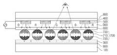
도 2는 본 발명의 일실시예에 따른 반사형 디스플레이장치의 단면도,2 is a cross-sectional view of a reflective display device according to an embodiment of the present invention;
도 3은 도 2에 도시한 마이크로캡슐의 전압인가에 따른 동작 상태단면도이다.3 is a cross-sectional view of an operating state according to voltage application of the microcapsules shown in FIG.
<도면의 주요 부분에 대한 부호의 설명><Explanation of symbols for the main parts of the drawings>
100:하부기판200:상부기판100: lower substrate 200: upper substrate
300:픽셀전극400:광원전극300: pixel electrode 400: light source electrode
500:광원600:공통전극500: light source 600: common electrode
700:마이크로캡슐710:유전액700: microcapsules 710: dielectric fluid
720:백색입자730:흑색입자720: white particles 730: black particles
800:보호막900:컬러필터800: protective film 900: color filter
본 발명은 디스플레이장치에 관한 것으로서, 보다 상세하게는 외부 광원으로 나온 빛이 반사형 디스플레이에 입사된 후 다시 반사판에 반사되어 표시화면을 사용자의 눈에 디스플레이 되게 하는 반사형 디스플레이장치에 관한 것이다.The present invention relates to a display device, and more particularly, to a reflective display device in which light emitted from an external light source is incident on a reflective display and then reflected back to a reflector to display a display screen in a user's eyes.
일반적으로, 액정표시장치는 광을 이용하는 방식에 따라 투과형과 반사형으로 대별된다.In general, liquid crystal displays are roughly classified into a transmission type and a reflection type according to a method of using light.
여기서, 투과형 액정표시장치는 두 장의 유리기판 사이에 액정물질이 주입된 액정표시패널과, 액정표시패널에 빛을 공급하는 백라이트(Back Light)를 구비하게 되는 바, 백라이트의 과도한 소비전력 및 부피, 무게로 인해 박형화, 경량화에 어려움이 있어, 근래에는 백라이트를 사용하지 않는 반사형 액정표시장치를 주로 사용하고 있다.The transmissive liquid crystal display device includes a liquid crystal display panel in which a liquid crystal material is injected between two glass substrates, and a backlight for supplying light to the liquid crystal display panel. Due to the weight, it is difficult to reduce the thickness and weight, and recently, a reflective liquid crystal display device which does not use a backlight is mainly used.
이러한, 반사형 액정표시장치는 자연광이 충분한 광량을 가지고 있지 않은 경우 표시된 정보를 볼 수 없게 되는 바, 이러한 문제를 해결하기 위해 광원을 공급하는 프론트라이트유닛(Front Light Unit; FLU)이 사용되고 있다.In the reflective liquid crystal display, when the natural light does not have a sufficient amount of light, the displayed information cannot be viewed. To solve this problem, a front light unit (FLU) for supplying a light source is used.
도 1은 프론트라이트유닛을 가지는 반사형 액정표시장치의 개략적 구조를 나타낸 도면이다.1 is a view showing a schematic structure of a reflective liquid crystal display device having a front light unit.
이러한, 반사형 액정표시장치는 반사형 액정패널(10)과, 반사형 액정패널(10) 상부에 구비된 상태로 빛을 공급하는 프론트라이트유닛(20)을 구비하는데, 상기 반사형 액정패널(10) 하단부에는 반사전극(Diffusing reflective electrode)(11)이 형성되어 액정패널(10)의 표시면에 입사되는 자연광이나 보조광을 반사되게 한다.The reflective liquid crystal display device includes a reflective
그리고, 상기 프론트라이트유닛(20)은 빛을 발생하는 광원(30)과, 빛을 액정패널의 표시면 방향으로 균일하게 출사시키는 도광판(40)과, 광원(30)에서 발생된 빛을 도광판(40) 방향으로 반사시키는 반사경(50)과, 도광판(40)에서 빛이 누설되는 것을 방지하는 반사방지막(60)으로 구성된다.The
여기서, 상기 도광판(40)은 상부표면이 프리즘 패턴으로 형성되어 도광판(40)에 경사지게 입사된 빛의 진행경로를 표시면에 대해 수직으로 변경되게 하며, 상기 도광판(40)에 의해 입사되는 빛은 반사형 액정패널(10)의 수직 방향으로 입사된 후 다시 반사형 액정패널(10)에 의해 반사되어 도광판(40) 상방으로 진행하여 사용자의 눈으로 입사되어 정보를 제공하게 된다.Here, the
그러나, 종래의 반사형 액정표시장치는 프론트라이트유닛(20)이 반사형 액정패널(10) 전면에 위치함으로 인해 화질이 저하되는 요인으로 작용되는 문제점이 있다.However, the conventional reflective liquid crystal display device has a problem in that the image quality is deteriorated because the
즉, 도광판(40)의 프리즘 패턴과 액정패널(10) 간의 간섭에 의한 모아레(Moire) 발생, 도광판(40)의 표면반사에 의한 명암비 저하, 도광판(40)의 투과율에 따른 휘도 저하 등이 발생하는 문제점이 있다.That is, moire occurs due to interference between the prism pattern of the
그리고, 도광판(40)이 프리즘 패턴으로 형성되어 조립시 외부 스크래치(scratch)나 먼지 흡착 등에 의해 쉽게 불량이 발생되는 문제점이 있다.In addition, since the
또한, 도광판(40)의 두께로 인하여 전체적인 디스플레이장치의 두께를 축소하는데 한계가 발생하는 문제점이 있다.In addition, there is a problem in that a limit occurs in reducing the thickness of the entire display apparatus due to the thickness of the
본 발명은 상술한 문제점을 해결하기 위해 창출된 것으로서, 화질저하 및 조립시 먼지흡착이나 스크래치에 의한 불량이 발생되지 않음과 더불어 두께를 얇게 할 수 있는 반사형 디스플레이장치를 제공하는 데 그 목적이 있다.SUMMARY OF THE INVENTION The present invention has been made to solve the above-mentioned problems, and an object thereof is to provide a reflective display device capable of reducing the image quality and reducing the thickness of the assembly and defects caused by dust absorption or scratching. .
본 발명의 다른 목적 및 장점들은 하기에 설명될 것이며, 본 발명의 실시예에 의해 알게 될 것이다. 또한, 본 발명의 목적 및 장점들은 특허청구범위에 나타낸 수단 및 조합에 의해 실현될 수 있다.Other objects and advantages of the invention will be described below and will be appreciated by the embodiments of the invention. Furthermore, the objects and advantages of the present invention can be realized by means and combinations indicated in the claims.
상기와 같은 목적을 달성하기 위한 본 발명의 반사형 디스플레이장치는, 상호 일정간격 이격되는 하부기판 및 상부기판과; 상기 하부기판 상면에 구비하는 복수개의 픽셀전극과; 복수개의 색상픽셀을 가지는 상태로 상기 상부기판 하면에 구비하는 컬러필터와; 상기 컬러필터의 각 색상픽셀 사이에 구비하는 복수개의 광원전극과; 각 상기 광원전극 하면에 결합되어 상기 하부기판 방향으로 빛을 발생하는 광원과; 상기 컬러필터 하면에 구비하는 공통전극; 및, 상기 공통전극과 상기 픽셀전극 사이에는 양 전하를 가지는 백색입자와 음 전하를 가지는 흑색입자 및 유전액으로 구성되는 복수개의 마이크로캡슐을 구비한다.Reflective display device of the present invention for achieving the above object, the lower substrate and the upper substrate spaced apart from each other by a predetermined interval; A plurality of pixel electrodes provided on an upper surface of the lower substrate; A color filter provided on a lower surface of the upper substrate while having a plurality of color pixels; A plurality of light source electrodes provided between each color pixel of the color filter; A light source coupled to a bottom surface of each light source electrode to generate light toward the lower substrate; A common electrode disposed on the bottom surface of the color filter; And a plurality of microcapsules comprising white particles having a positive charge, black particles having a negative charge, and a dielectric liquid between the common electrode and the pixel electrode.
여기서, 상기 하부기판과 픽셀전극 및 상기 상부기판과 광원전극 사이에는 외부로부터 수분이나 산소의 침투를 막는 보호막이 구비하는 것이 바람직하다.Here, it is preferable that a protective film is provided between the lower substrate and the pixel electrode and the upper substrate and the light source electrode to prevent the penetration of moisture or oxygen from the outside.
그리고, 상기 보호막은 아크릴(Acryl), 폴리이미드(Polyimide), 산화실리콘(Si02), 질화규소(SiN) 중 선택된 어느하나의 재질인 것이 바람직하다.The protective film is preferably made of any one selected from acryl, polyimide, silicon oxide (Si02 ), and silicon nitride (SiN).
또한, 상기 광원전극은 블랙 매트릭스(Black matrix)인 것이 바람직하다.In addition, the light source electrode is preferably a black matrix.
또한, 상기 광원은 백색 유기발광다이오드(White OLED)인 것이 바람직하다.In addition, the light source is preferably a white organic light emitting diode (White OLED).
또한, 상기 광원은 상기 광원전극보다 작은 것이 바람직하다.In addition, the light source is preferably smaller than the light source electrode.
이하 첨부된 도면을 참조로 본 발명의 바람직한 실시예들을 상세히 설명하기로 한다.Hereinafter, exemplary embodiments of the present invention will be described in detail with reference to the accompanying drawings.
이에 앞서, 본 명세서 및 청구범위에 사용된 용어나 단어는 통상적이거나 사전적인 의미로 한정해서 해석되어서는 아니되며, 발명자는 그 자신의 발명을 가장 최선의 방법으로 설명하기 위해 용어의 개념을 적절하게 정의할 수 있다는 원칙에 입각하여 본 발명의 기술적인 사상에 부합하는 의미와 개념으로 해석되어야만 한다.Prior to this, terms or words used in the specification and claims should not be construed as having a conventional or dictionary meaning, and the inventors should properly explain the concept of terms in order to best explain their own invention. It should be interpreted as meanings and concepts corresponding to the technical idea of the present invention based on the principle of definition.
따라서, 본 명세서에 기재된 실시예와 도면에 도시된 구성은 본 발명의 가장 바람직한 일 실시예에 불과할 뿐이고 본 발명의 기술적 사상을 모두 대변하는 것은 아니므로, 본 출원시점에 있어서 이들을 대체할 수 있는 다양한 균등물과 변형예들이 있을 수 있음을 이해하여야 한다.Therefore, the embodiments described in the specification and the drawings shown in the drawings are only the most preferred embodiment of the present invention and do not represent all of the technical idea of the present invention, various modifications that can be replaced at the time of the present application It should be understood that there may be equivalents and variations.
도 2는 본 발명의 일실시예에 따른 반사형 디스플레이장치의 전체 단면도이다.2 is an overall cross-sectional view of a reflective display device according to an embodiment of the present invention.
도시된 바와 같이, 본 발명의 일실시예에 따른 반사형 디스플레이장치는, 하부기판(100), 상부기판(200), 픽셀전극(300), 컬러필터(900), 광원전극(400), 광원(500), 공통전극(600), 마이크로캡슐(700)을 구비하고 있다.As shown, the reflective display device according to an embodiment of the present invention, the
상기 하부기판(100) 및 상기 상부기판(200)은 상호 일정간격 이격되는 기판이다The
이러한, 각각의 상기 하부기판(100) 및 상기 상부기판(200)은 상면 및 하면이 평평한 기판으로, 투명하거나 불투명한 것을 선택적으로 형성할 수 있다.Each of the
즉, 상기 하부기판(100) 및 상기 상부기판(200)은 유리나 플라스틱 필름 중 선택된 어느하나의 재질로 형성하는 것이 바람직하다.That is, the
상기 픽셀전극(300)은 상기 하부기판(100) 상면에 복수개가 구비되어 구동 전압을 인가받는 전극이다.The
상기 컬러필터(900)는 상기 상부기판 하면에 구비하는 필터이다.The
이러한, 상기 컬러필터(900)는 복수개의 레드(R), 그린(G), 블루(B)를 가지는 색상픽셀을 가지고 있다.The
상기 광원전극(400)은 상기 광원(500)에 구동 전압을 인가하여 상기 광원(500)에서 빛을 발생되게 하는 복수개의 전극이다.The
이러한, 상기 광원전극(400)은 상기 컬러필터(900)의 각 색상픽셀 사이에 구비하는 것이 바람직하다.The
그리고, 상기 광원전극(400)은 상기 광원(500)에서 빛이 발생할 경우, 상기 상부기판(200) 방향으로 향하지 않고 상기 하부기판(100) 방향으로만 향할 수 있도록 블랙 매트릭스(Black matrix)인 것이 바람직하다.In addition, when light is generated from the
여기서, 상기 광원전극(400)은 크롬(Cr), 크롬산화물(Cr0x)을 스퍼터링(Sputtering)공법으로 침전시킨 후 포토리소그래피(Photo-lithography)공법으로 패터닝하여 블랙 매트릭스로 형성할 수 있다.Here, the
이같이, 상기 광원전극(400)이 블랙 매트릭스을 특성으로 가지는 상태로 상기 컬러필터(900)의 각 색상픽셀 사이에 구비됨으로써, 외부로부터 입사되는 빛이 상기 컬러필터(900)의 각 색상픽셀의 개구부만을 통과하고 각각의 색상픽셀 사이나 스위칭소자 및 배선부분 등 색상을 조절할 수 없는 부분으로 투과되는 것을 방지하여 디스플레이의 대조비를 향상되게 한다.In this way, the
상기 광원(500)은 상기 광원전극(400)으로 인가되는 구동 전압에 의해 빛을 발생되게 하는 소자이다.The
이러한, 상기 광원(500)은 각각의 상기 광원전극(400) 하면에 결합되어 상기 광원전극(400) 전극에 구동 전압이 인가시 상기 하부기판(100) 방향으로 발광하게 된다.The
이러한, 상기 광원(500)은 저전압 구동이 가능한 백색 유기발광다이오드(White OLED)를 사용하는 것이 바람직하다.The
그리고, 상기 광원(500)은 빛이 상기 상부기판(200) 방향으로 향하지 않고 상기 하부기판(100) 방향으로만 향할 수 있도록 상기 광원전극(400)보다 작게 형성함과 더불어 배면발광(Bottom Emission)방식인 것을 사용하는 것이 바람직하다.In addition, the
더불어, 상기 하부기판(100)과 상기 픽셀전극(300) 및, 상기 상부기판(200)과 상기 광원전극(400) 사이에는 외부로부터 수분이나 산소가 침투하는 것을 방지하여 상기 광원(500)의 수명을 연장되게 하는 보호막(800)을 구비한다.In addition, between the
이러한, 상기 보호막(800)은 아크릴(Acryl), 폴리이미드(Polyimide)과 같은 고분자소재나, 산화실리콘(Si02), 질화규소(SiN)와 같은 세라믹소재 중 선택된 어느 하나의 재질로 형성하는 것이 바람직하다.The
상기 공통전극(600)은 상기 컬러필터(800) 하면에 구비되어 구동 전압을 인가받는 투명전극이다.The
이러한, 상기 공통전극(600)은 상기 광원전극(400)과 연결되어 상기 상부기판(200) 상에 소자의 구동 전압 인가 및 상기 광원(500)으로 구동 전압을 동시에 인가되게 한다.The
상기 마이크로캡슐(700)은 상기 공통전극(600)과 상기 픽셀전극(300) 사이에 위치하게 되는 캡슐이다.The
이러한, 상기 마이크로캡슐(700)은 투명한 유전액(710)(Dielectric fluid)과, 양의 전하를 가지는 백색입자(720) 및, 음의 전하를 가지는 흑색입자(730)를 구비한다.The
따라서, 도 3에 도시한 바와 같이 상기 마이크로캡슐(700)은 상기 공통전극(600) 및 상기 픽셀전극(300)에 인가되는 전위에 따라 양의 전하를 가지는 백색입자(720) 및, 음의 전하를 가지는 흑색입자(730)의 위치가 정해진다.Accordingly, as shown in FIG. 3, the
즉, 상기 공통전극(600)은 양전극으로 인가됨과 더불어 상기 픽셀전극(300)이 음전극으로 인가되면, 흑색입자(730)는 상기 공통전극(600)으로 이동하게 되며, 백색입자(720)는 상기 픽셀전극(300)으로 이동하게 된다.That is, when the
반대로, 상기 공통전극(600)은 음전극으로 인가됨과 더불어 상기 픽셀전극(300)이 양전극으로 인가되면, 흑색입자(730)는 상기 픽셀전극(300)으로 이동하게 되며, 백색입자(720)는 상기 공통전극(600)으로 이동하게 된다.On the contrary, when the
이와 같이, 상기 공통전극(600) 방향으로 이동된 입자가 흑색입자(730)일 경우에는 상기 광원(500)으로부터 발생된 빛이 상기 마이크로캡슐(700)에 반사된 후 외부에서 흑색으로 디스플레이되게 하며, 상기 공통전극(600) 방향으로 이동된 입자가 백색입자(720)일 경우에는 상기 광원(500)으로부터 발생된 빛이 상기 마이크로캡슐(700)에 반사된 후 외부에서 백색으로 디스플레이되게 한다.As such, when the particles moved toward the
그리고, 상기 마이크로캡슐(700)의 백색입자(720)에 의해 반사되는 빛은 상기 컬러필터(900)에 의해 다른 다양한 색으로 변환하여 외부에서 다양한 색상을 가지는 상태로 디스플레이된다.In addition, the light reflected by the
이와 같이, 구성되는 본 발명의 일실시예에 따른 반사형 디스플레이장치의 동작을 도 2 및 도 3을 참조하여 설명하면 다음과 같다.As described above, the operation of the reflective display device according to the embodiment of the present invention will be described with reference to FIGS. 2 and 3.
먼저, 상기 공통전극(600) 및 상기 픽셀전극(300)에 구동 전압을 인가하면, 상기 광원전극(400)을 통해 상기 광원(500)으로부터 발생되는 빛이 상기 픽셀전극(300) 방향을 향하게 된다.First, when a driving voltage is applied to the
더불어, 상기 공통전극(600) 및 상기 픽셀전극(300)에 인가되는 전위에 따라 상기 마이크로캡슐(700)의 양의 전하를 가지는 백색입자(720) 및, 음의 전하를 가지는 흑색입자(730) 위치가 이동하게 된다.In addition, the
상기 공통전극(600)이 음전극으로 인가되면 상기 공통전극(600) 방향으로 양의 전하를 가지는 백색입자(720)가 이동하면서 상기 광원(500)으로부터 발생되는 빛이 백색입자(720)에 의해 반사되어 외부에서는 백색이나 그 외 상기 컬러필터(900)에 의해 RGB(레드, 그린, 블루)로 변환된 색상으로 디스플레이된다.When the
더불어, 상기 공통전극(600)이 양전극으로 인가되면 상기 공통전극(600) 방향으로 음의 전하를 가지는 흑색입자(730)가 이동하면서 상기 광원(500)으로부터 발생되는 빛이 흑색입자(730)에 의해 반사되어 외부에서는 흑색으로 디스플레이되면서 전체적인 디스플레이 형상을 파악할 수 있게 된다.In addition, when the
이와 같은, 본 발명의 반사형 디스플레이장치는 상기 하부기판(100) 방향으로 빛을 발생하는 상기 광원(500)을 평평한 상기 상부기판(200) 하면에 일체 상태로 구비 하여 상기 광원(500)에서 발생되는 빛이 상기 마이크로캡슐(700)에 의해 반사된 후 왜곡없이 디스플레이됨으로써 주변광이 약하거나 어두울 경우에도 화질이 우수하게 된다.As described above, the reflective display device of the present invention is provided with the
더불어, 상기 광원(500)을 상부기판(200) 하면에 일체 상태로 구비하여 두께가 얇아지며, 조립을 용이하게 할 수 있게 된다.In addition, the
이상과 같이 본 발명은 비록 한정된 실시예와 도면에 의해 설명되었으나, 본 발명은 이것에 의해 한정되지 않으며 본 발명이 속하는 기술분야에서 통상의 지식을 가진 자에 의해 본 발명의 기술 사상과 아래에 기재될 특허청구범위의 균등범위 내에서 다양한 수정 및 변형이 가능함은 물론이다.As described above, although the present invention has been described by way of limited embodiments and drawings, the present invention is not limited thereto and is described by the person of ordinary skill in the art to which the present invention pertains. Various modifications and variations are possible without departing from the scope of the appended claims.
상술한 바와 같은 본 발명의 반사형 디스플레이장치에 따르면 다음과 같은 효과를 제공한다.According to the reflective display device of the present invention as described above provides the following effects.
첫째, 하부기판 방향으로 빛을 발생하는 광원을 평평한 상부기판 하면에 일체 상태로 구비하여 광원에서 발생되는 빛이 마이크로캡슐에 의해 반사된 후 왜곡없이 디스플레이됨으로써 주변광이 약하거나 어두울 경우도 화질이 우수하게 된다.First, the light source that emits light toward the lower substrate direction is integrated on the lower surface of the flat upper substrate so that the light generated from the light source is reflected by the microcapsule and displayed without distortion. Done.
둘째, 광원을 상부기판 하면에 일체 상태로 구비하여 전체 장치의 두께가 얇아짐과 더불어 조립을 용이하게 할 수 있게 된다.Second, the light source is provided on the lower surface of the upper substrate in an integrated state so that the thickness of the entire apparatus can be reduced and the assembly can be facilitated.
Claims (6)
Translated fromKoreanPriority Applications (2)
| Application Number | Priority Date | Filing Date | Title |
|---|---|---|---|
| KR1020070003468AKR20080066255A (en) | 2007-01-11 | 2007-01-11 | Reflective Display Device |
| PCT/KR2007/000989WO2008084898A1 (en) | 2007-01-11 | 2007-02-27 | Reflection-type display system |
Applications Claiming Priority (1)
| Application Number | Priority Date | Filing Date | Title |
|---|---|---|---|
| KR1020070003468AKR20080066255A (en) | 2007-01-11 | 2007-01-11 | Reflective Display Device |
Publications (1)
| Publication Number | Publication Date |
|---|---|
| KR20080066255Atrue KR20080066255A (en) | 2008-07-16 |
Family
ID=39608774
Family Applications (1)
| Application Number | Title | Priority Date | Filing Date |
|---|---|---|---|
| KR1020070003468ACeasedKR20080066255A (en) | 2007-01-11 | 2007-01-11 | Reflective Display Device |
Country Status (2)
| Country | Link |
|---|---|
| KR (1) | KR20080066255A (en) |
| WO (1) | WO2008084898A1 (en) |
Cited By (2)
| Publication number | Priority date | Publication date | Assignee | Title |
|---|---|---|---|---|
| KR20170084408A (en)* | 2016-01-11 | 2017-07-20 | 삼성디스플레이 주식회사 | Organic light emitting display device |
| US10082698B2 (en) | 2016-01-13 | 2018-09-25 | Samsung Display Co., Ltd. | Display device and method of manufacturing the same |
Families Citing this family (3)
| Publication number | Priority date | Publication date | Assignee | Title |
|---|---|---|---|---|
| CN103365021B (en)* | 2012-04-03 | 2015-11-25 | 元太科技工业股份有限公司 | Electrophoretic display device capable of switching between color mode and black-and-white mode |
| CN105182653A (en)* | 2015-09-14 | 2015-12-23 | 京东方科技集团股份有限公司 | Electrophoresis display panel and electrophoresis display device |
| CN107664837A (en)* | 2017-10-20 | 2018-02-06 | 京东方科技集团股份有限公司 | A kind of reflective display |
Citations (3)
| Publication number | Priority date | Publication date | Assignee | Title |
|---|---|---|---|---|
| JP2003195362A (en)* | 2001-12-25 | 2003-07-09 | Seiko Epson Corp | Electrophoretic display and electronic equipment |
| JP2004302321A (en)* | 2003-03-31 | 2004-10-28 | Seiko Epson Corp | Display device, electronic device, and display method |
| JP2005107246A (en)* | 2003-09-30 | 2005-04-21 | Seiko Epson Corp | Reflective display device |
Family Cites Families (1)
| Publication number | Priority date | Publication date | Assignee | Title |
|---|---|---|---|---|
| KR20050110392A (en)* | 2004-05-18 | 2005-11-23 | 엘지.필립스 엘시디 주식회사 | Electrophoretic display device |
- 2007
- 2007-01-11KRKR1020070003468Apatent/KR20080066255A/ennot_activeCeased
- 2007-02-27WOPCT/KR2007/000989patent/WO2008084898A1/enactiveApplication Filing
Patent Citations (3)
| Publication number | Priority date | Publication date | Assignee | Title |
|---|---|---|---|---|
| JP2003195362A (en)* | 2001-12-25 | 2003-07-09 | Seiko Epson Corp | Electrophoretic display and electronic equipment |
| JP2004302321A (en)* | 2003-03-31 | 2004-10-28 | Seiko Epson Corp | Display device, electronic device, and display method |
| JP2005107246A (en)* | 2003-09-30 | 2005-04-21 | Seiko Epson Corp | Reflective display device |
Cited By (2)
| Publication number | Priority date | Publication date | Assignee | Title |
|---|---|---|---|---|
| KR20170084408A (en)* | 2016-01-11 | 2017-07-20 | 삼성디스플레이 주식회사 | Organic light emitting display device |
| US10082698B2 (en) | 2016-01-13 | 2018-09-25 | Samsung Display Co., Ltd. | Display device and method of manufacturing the same |
Also Published As
| Publication number | Publication date |
|---|---|
| WO2008084898A1 (en) | 2008-07-17 |
Similar Documents
| Publication | Publication Date | Title |
|---|---|---|
| KR20250078866A (en) | Display device | |
| JP2000075293A (en) | Illumination device, illuminated touch panel and reflective liquid crystal display device | |
| CN209215800U (en) | display device | |
| US20160004067A1 (en) | Display panel, manufacturing method thereof, and display device | |
| TW201533510A (en) | Backlight assembly and liquid crystal display including the same | |
| WO2020095607A1 (en) | Electronic apparatus | |
| WO2012173308A1 (en) | Liquid micro-shutter display apparatus | |
| JP2004145275A (en) | Colored layer material, color filter substrate, electro-optical device and electronic equipment, method for manufacturing color filter substrate, and method for manufacturing electro-optical device | |
| KR20080066255A (en) | Reflective Display Device | |
| US20060125982A1 (en) | Liquid crystal display | |
| KR20130030441A (en) | Liquid crystal display device | |
| KR20110022970A (en) | Display | |
| KR20190143243A (en) | LED Module and backlight Module having the same and Display Device having the same | |
| JP2004062060A (en) | Liquid crystal display | |
| KR102408905B1 (en) | Display Device | |
| US8823900B2 (en) | Illumination device and electrooptic apparatus | |
| JP7719094B2 (en) | Display device and method for manufacturing the same | |
| KR20190075435A (en) | Display Device | |
| JP2024054568A (en) | Display device | |
| JP2007333943A (en) | Electrooptical device, electronic device and manufacturing method of electrooptical device | |
| KR101296642B1 (en) | Organic Lighting Emmiting Device | |
| KR20100067820A (en) | Liquid crystal display device with improved light-leakage property | |
| KR102782935B1 (en) | Display panel and display apparatus including same | |
| US11852857B2 (en) | Display device | |
| KR20090054756A (en) | High brightness transflective liquid crystal display device and manufacturing method thereof |
Legal Events
| Date | Code | Title | Description |
|---|---|---|---|
| A201 | Request for examination | ||
| PA0109 | Patent application | Patent event code:PA01091R01D Comment text:Patent Application Patent event date:20070111 | |
| PA0201 | Request for examination | ||
| E902 | Notification of reason for refusal | ||
| PE0902 | Notice of grounds for rejection | Comment text:Notification of reason for refusal Patent event date:20071212 Patent event code:PE09021S01D | |
| E902 | Notification of reason for refusal | ||
| PE0902 | Notice of grounds for rejection | Comment text:Notification of reason for refusal Patent event date:20080526 Patent event code:PE09021S01D | |
| PG1501 | Laying open of application | ||
| E90F | Notification of reason for final refusal | ||
| PE0902 | Notice of grounds for rejection | Comment text:Final Notice of Reason for Refusal Patent event date:20081112 Patent event code:PE09021S02D | |
| E601 | Decision to refuse application | ||
| E801 | Decision on dismissal of amendment | ||
| PE0601 | Decision on rejection of patent | Patent event date:20090501 Comment text:Decision to Refuse Application Patent event code:PE06012S01D Patent event date:20081112 Comment text:Final Notice of Reason for Refusal Patent event code:PE06011S02I Patent event date:20080526 Comment text:Notification of reason for refusal Patent event code:PE06011S01I Patent event date:20071212 Comment text:Notification of reason for refusal Patent event code:PE06011S01I | |
| PE0801 | Dismissal of amendment | Patent event code:PE08012E01D Comment text:Decision on Dismissal of Amendment Patent event date:20090501 Patent event code:PE08011R01I Comment text:Amendment to Specification, etc. Patent event date:20090112 Patent event code:PE08011R01I Comment text:Amendment to Specification, etc. Patent event date:20080728 Patent event code:PE08011R01I Comment text:Amendment to Specification, etc. Patent event date:20080212 |