KR20080061030A - Metal wiring formation method of semiconductor device - Google Patents
Metal wiring formation method of semiconductor deviceDownload PDFInfo
- Publication number
- KR20080061030A KR20080061030AKR1020060135767AKR20060135767AKR20080061030AKR 20080061030 AKR20080061030 AKR 20080061030AKR 1020060135767 AKR1020060135767 AKR 1020060135767AKR 20060135767 AKR20060135767 AKR 20060135767AKR 20080061030 AKR20080061030 AKR 20080061030A
- Authority
- KR
- South Korea
- Prior art keywords
- conductive barrier
- layer
- semiconductor substrate
- forming
- metal
- Prior art date
- Legal status (The legal status is an assumption and is not a legal conclusion. Google has not performed a legal analysis and makes no representation as to the accuracy of the status listed.)
- Ceased
Links
- 229910052751metalInorganic materials0.000titleclaimsabstractdescription93
- 239000002184metalSubstances0.000titleclaimsabstractdescription93
- 239000004065semiconductorSubstances0.000titleclaimsabstractdescription56
- 238000000034methodMethods0.000titleclaimsabstractdescription38
- 230000015572biosynthetic processEffects0.000titledescription2
- 230000004888barrier functionEffects0.000claimsabstractdescription105
- 239000000758substrateSubstances0.000claimsabstractdescription31
- 238000007517polishing processMethods0.000claimsabstractdescription26
- 239000000126substanceSubstances0.000claimsabstractdescription26
- 230000008569processEffects0.000claimsabstractdescription17
- RYGMFSIKBFXOCR-UHFFFAOYSA-NCopperChemical compound[Cu]RYGMFSIKBFXOCR-UHFFFAOYSA-N0.000claimsabstractdescription14
- 229910052802copperInorganic materials0.000claimsabstractdescription14
- 239000010949copperSubstances0.000claimsabstractdescription14
- 238000000151depositionMethods0.000claimsabstractdescription5
- 238000005530etchingMethods0.000claimsdescription10
- 229920002120photoresistant polymerPolymers0.000claimsdescription9
- 238000000231atomic layer depositionMethods0.000claimsdescription8
- 238000005229chemical vapour depositionMethods0.000claimsdescription8
- 238000005240physical vapour depositionMethods0.000claimsdescription8
- 239000002002slurrySubstances0.000claimsdescription6
- 239000000463materialSubstances0.000claimsdescription5
- 230000008901benefitEffects0.000abstractdescription3
- 239000010410layerSubstances0.000description100
- 239000010408filmSubstances0.000description47
- 238000010586diagramMethods0.000description4
- 238000004519manufacturing processMethods0.000description4
- 239000005368silicate glassSubstances0.000description4
- 125000006850spacer groupChemical group0.000description4
- ATJFFYVFTNAWJD-UHFFFAOYSA-NTinChemical compound[Sn]ATJFFYVFTNAWJD-UHFFFAOYSA-N0.000description3
- 239000003795chemical substances by applicationSubstances0.000description3
- 238000009792diffusion processMethods0.000description3
- 239000011229interlayerSubstances0.000description3
- WFKWXMTUELFFGS-UHFFFAOYSA-NtungstenChemical compound[W]WFKWXMTUELFFGS-UHFFFAOYSA-N0.000description3
- 229910052721tungstenInorganic materials0.000description3
- 239000010937tungstenSubstances0.000description3
- BHEPBYXIRTUNPN-UHFFFAOYSA-Nhydridophosphorus(.) (triplet)Chemical compound[PH]BHEPBYXIRTUNPN-UHFFFAOYSA-N0.000description2
- 238000009413insulationMethods0.000description2
- 238000002955isolationMethods0.000description2
- 230000004048modificationEffects0.000description2
- 238000012986modificationMethods0.000description2
- 239000010409thin filmSubstances0.000description2
- ZOXJGFHDIHLPTG-UHFFFAOYSA-NBoronChemical compound[B]ZOXJGFHDIHLPTG-UHFFFAOYSA-N0.000description1
- 229910001111Fine metalInorganic materials0.000description1
- YCKRFDGAMUMZLT-UHFFFAOYSA-NFluorine atomChemical compound[F]YCKRFDGAMUMZLT-UHFFFAOYSA-N0.000description1
- 229910045601alloyInorganic materials0.000description1
- 239000000956alloySubstances0.000description1
- 229910052782aluminiumInorganic materials0.000description1
- XAGFODPZIPBFFR-UHFFFAOYSA-NaluminiumChemical compound[Al]XAGFODPZIPBFFR-UHFFFAOYSA-N0.000description1
- 229910052796boronInorganic materials0.000description1
- 230000008859changeEffects0.000description1
- 230000007423decreaseEffects0.000description1
- 230000000694effectsEffects0.000description1
- 229910052731fluorineInorganic materials0.000description1
- 239000011737fluorineSubstances0.000description1
- 238000000206photolithographyMethods0.000description1
- 238000001039wet etchingMethods0.000description1
Images


Classifications
- H—ELECTRICITY
- H01—ELECTRIC ELEMENTS
- H01L—SEMICONDUCTOR DEVICES NOT COVERED BY CLASS H10
- H01L21/00—Processes or apparatus adapted for the manufacture or treatment of semiconductor or solid state devices or of parts thereof
- H01L21/70—Manufacture or treatment of devices consisting of a plurality of solid state components formed in or on a common substrate or of parts thereof; Manufacture of integrated circuit devices or of parts thereof
- H01L21/71—Manufacture of specific parts of devices defined in group H01L21/70
- H01L21/768—Applying interconnections to be used for carrying current between separate components within a device comprising conductors and dielectrics
- H01L21/76838—Applying interconnections to be used for carrying current between separate components within a device comprising conductors and dielectrics characterised by the formation and the after-treatment of the conductors
- H01L21/76841—Barrier, adhesion or liner layers
- H01L21/76843—Barrier, adhesion or liner layers formed in openings in a dielectric
- H01L21/76849—Barrier, adhesion or liner layers formed in openings in a dielectric the layer being positioned on top of the main fill metal
- H—ELECTRICITY
- H01—ELECTRIC ELEMENTS
- H01L—SEMICONDUCTOR DEVICES NOT COVERED BY CLASS H10
- H01L21/00—Processes or apparatus adapted for the manufacture or treatment of semiconductor or solid state devices or of parts thereof
- H01L21/02—Manufacture or treatment of semiconductor devices or of parts thereof
- H01L21/04—Manufacture or treatment of semiconductor devices or of parts thereof the devices having potential barriers, e.g. a PN junction, depletion layer or carrier concentration layer
- H01L21/18—Manufacture or treatment of semiconductor devices or of parts thereof the devices having potential barriers, e.g. a PN junction, depletion layer or carrier concentration layer the devices having semiconductor bodies comprising elements of Group IV of the Periodic Table or AIIIBV compounds with or without impurities, e.g. doping materials
- H01L21/28—Manufacture of electrodes on semiconductor bodies using processes or apparatus not provided for in groups H01L21/20 - H01L21/268
Landscapes
- Engineering & Computer Science (AREA)
- Physics & Mathematics (AREA)
- Condensed Matter Physics & Semiconductors (AREA)
- General Physics & Mathematics (AREA)
- Manufacturing & Machinery (AREA)
- Computer Hardware Design (AREA)
- Microelectronics & Electronic Packaging (AREA)
- Power Engineering (AREA)
- Internal Circuitry In Semiconductor Integrated Circuit Devices (AREA)
Abstract
Translated fromKoreanDescription
Translated fromKorean도 1은 본 발명에서 구현한 반도체 소자의 단면도이다.1 is a cross-sectional view of a semiconductor device implemented in the present invention.
도 2 내지 도 7은 본 발명에 따른 반도체 소자의 금속 배선 형성 방법을 설명하는 공정도이다.2 to 7 are process charts illustrating a metal wiring formation method of a semiconductor device according to the present invention.
도 7a~도7d는 본 발명에서 제안하는 전도성 배리어막의 제조 공정도이다.7A to 7D are manufacturing process diagrams of the conductive barrier film proposed in the present invention.
도 8a~도8c는 본 발명에서 제안하는 전도성 배리어막의 또 다른 제조 공정도이다.8A to 8C are still another manufacturing process chart of the conductive barrier film proposed in the present invention.
본 발명은 반도체 소자의 금속 배선 형성 방법에 관한 것이다.The present invention relates to a method for forming metal wiring of a semiconductor device.
일반적으로 반도체 소자의 금속 배선은 알루미늄 및 그 합금, 구리 등의 금속 박막을 이용하여 반도체 소자 사이의 전기적 접속 및 패드 접속을 통해 반도체 기판 내에 형성되어 있는 회로를 연결한다.Generally, the metal wiring of a semiconductor element connects the circuit formed in the semiconductor substrate through the electrical connection and pad connection between semiconductor elements using metal thin films, such as aluminum, its alloy, and copper.
이러한 금속 배선의 형성은 산화막 등의 절연막에 의해 격리된 소자 전극 및 패드를 연결하기 위하여, 먼저 절연막을 선택적으로 식각하여 접촉구를 형성하고, 베리어 메탈과 텅스텐 등을 이용하여 접촉구를 채우는 금속 플러그를 형성한다. 그리고, 상부에 금속 박막을 형성하고, 패터닝(patterning)하여 소자 전극 및 패드를In order to connect the device electrodes and pads separated by an insulating film such as an oxide film, the metal wiring is first formed by selectively etching an insulating film to form a contact hole, and a metal plug filling a contact hole using barrier metal and tungsten. To form. Then, a metal thin film is formed on the upper portion and patterned to form the device electrode and the pad.
접속하기 위한 금속 배선을 형성한다.Metal wiring for connection is formed.
이와 같은 금속 배선을 패터닝하기 위하여 주로 포토리소그래피 공정을 이용하는 데, 반도체 소자의 미세화에 따라 금속 배선의 임계 사이즈(critical dimension)가 점차적으로 작아져 금속 배선의 미세 패턴을 형성하는 데 어려움이 있다.In order to pattern such metal wires, photolithography is mainly used. As the semiconductor device becomes smaller, the critical dimension of the metal wires gradually decreases, making it difficult to form fine patterns of the metal wires.
따라서, 이러한 미세 패턴의 금속 배선을 용이하게 형성하기 위하여 도입된 것이 다마신(damascene) 공정이다.Therefore, a damascene process is introduced to easily form such a fine metal wiring.
이러한 다마신 공정을 통해 만들어지는 금속 배선은 다층 구조로 만들어질 수 있는데, 구리로 이루어진 다층 구조의 금속 배선의 경우에는 하부의 구리 금속배선이 상부의 구리 금속 배선을 둘러싸고 있는 상부 금속간 절연막(inter-metal dielectric) 내로 확산되는 것을 방지하기 위해 하부 구리 금속 배선 및 하부 금속 간 절연막 전면에 SiN과 SiCN 등의 물질로 이루어진 배리어막(barrier layer)을 만든다.The metal wirings made through the damascene process may be made of a multilayer structure. In the case of a metal wiring having a multilayer structure made of copper, an upper intermetallic insulating layer (inter) in which a lower copper metal wiring surrounds an upper copper metal wiring A barrier layer made of a material such as SiN and SiCN is formed on the entire surface of the lower copper metal wiring and the lower metal interlayer to prevent diffusion into the metal dielectric.
한편, 이와 같이 배리어막이 하부 구리 금속 배선 및 하부 금속간 절연막 전면에 존재함에 따라 하부 금속간 절연막의 유전율(effective k)이 높아져 RC 지연이 생김으로써 반도체 소자의 신뢰성이 저하될 수 있다.On the other hand, as the barrier film is present on the entire lower copper metal wiring and the lower intermetallic insulating film as described above, an effective k of the lower intermetallic insulating film is increased to cause an RC delay, thereby reducing the reliability of the semiconductor device.
본 발명에서는 반도체 소자의 배리어막으로 인해 금속간 절연막의 유전율이 높아지는 것을 방지하여 반도체 소자의 신뢰성을 향상할 수 있는 반도체 소자의 금속 배선 형성 방법을 제공하는 것이다.The present invention provides a method for forming a metal wiring of a semiconductor device that can prevent the dielectric constant of the intermetallic insulating film from increasing due to the barrier film of the semiconductor device and improve the reliability of the semiconductor device.
본 발명에 따른 반도체 소자의 금속 배선 형성 방법의 제 1 실시예는 절연막이 형성된 반도체 기판을 제공하는 단계; 상기 절연막에 비아홀 및 트렌치로 이루어지는 개구부를 형성하는 단계; 상기 개구부의 내벽에 제 1 전도성 배리어막을 형성하기 위하여 상기 반도체 기판의 전면에 상기 제 1 전도성 배리어막을 증착하는 단계; 상기 제 1 전도성 배리어막이 형성된 상기 반도체 기판의 전면에 금속층을 형성하는 단계; 상기 절연막이 노출될 때까지 상기 금속층 및 제 1 전도성 배리어막에 대하여 화학 기계적 연마 공정을 수행하는 단계; 상기 반도체 기판의 전면에 제 2 전도성 배리어막을 형성하는 단계; 상기 절연막이 노출될 때까지 상기 제 2 전도성 배리어막에 대하여 화학 기계적 연마 공정을 수행하는 단계; 를 포함하는 것을 특징으로 한다.A first embodiment of a method for forming metal wirings of a semiconductor device according to the present invention comprises the steps of providing a semiconductor substrate having an insulating film; Forming an opening made of a via hole and a trench in the insulating film; Depositing the first conductive barrier film on the entire surface of the semiconductor substrate to form a first conductive barrier film on an inner wall of the opening; Forming a metal layer on an entire surface of the semiconductor substrate on which the first conductive barrier film is formed; Performing a chemical mechanical polishing process on the metal layer and the first conductive barrier layer until the insulating layer is exposed; Forming a second conductive barrier layer on the entire surface of the semiconductor substrate; Performing a chemical mechanical polishing process on the second conductive barrier film until the insulating film is exposed; Characterized in that it comprises a.
제 1 실시예에서, 상기 제 2 전도성 배리어막에 대한 화학 기계적 연마 공정에 의하여 상기 개부부의 상면에만 상기 제 2 전도성 배리어막이 잔존하는 것을 특징으로 한다.In the first embodiment, the second conductive barrier film remains on only the upper surface of the opening part by a chemical mechanical polishing process for the second conductive barrier film.
제 1 실시예에서, 상기 화학 기계적 연마 공정에서 사용되는 슬러리(slurry)는 상기 제 1 전도성 배리어막보다 상기 금속층에 대한 식각 선택비가 높은 물질인 것을 특징으로 한다.In the first embodiment, the slurry used in the chemical mechanical polishing process is a material having a higher etching selectivity with respect to the metal layer than the first conductive barrier film.
제 1 실시예에서, 상기 금속층은 구리로 이루어지는 것을 특징으로 한다.In the first embodiment, the metal layer is characterized in that the copper.
제 1 실시예에서, 상기 제 1 및 제2 배리어막은 화학 기상 증착(chemical vapor deposition, CVD), 물리적 증착(physical vapor deposition, PVD) 또는 원자층 증착(atomic layerdeposition, ALD) 방법에 의하여 형성되는 것을 특징으로 한다.In the first embodiment, the first and second barrier films are formed by chemical vapor deposition (CVD), physical vapor deposition (PVD) or atomic layer deposition (ALD) method. It features.
본 발명에 따른 반도체 소자의 금속 배선 형성 방법의 제 2 실시예는 절연막이 형성된 반도체 기판을 제공하는 단계; 상기 절연막에 비아홀 및 트렌치로 이루어지는 개구부를 형성하는 단계; 상기 개구부의 내벽에 제 1 전도성 배리어막을 형성하기 위하여 상기 반도체 기판의 전면에 상기 제 1 전도성 배리어막을 증착하는 단계; 상기 제 1 전도성 배리어막이 형성된 상기 반도체 기판의 전면에 금속층을 형성하는 단계; 상기 절연막이 노출될 때까지 상기 금속층 및 제 1 전도성 배리어막에 대하여 화학 기계적 연마 공정을 수행하는 단계; 상기 반도체 기판의 전면에 제 2 전도성 배리어막을 형성하는 단계; 상기 개구부상에 형성되어 있는 제 2 전도성 배리어막상에 상기 개구부에 대응하는 사이즈의 감광제 패턴을 형성하는 단계; 상기 반도체 기판의 상면에 노출되어 있는 제 2 전도성 배리어막을 식각 공정에 의하여 제거하는 단계; 상기 감광제 패턴을 제거하는 단계; 를 포함하는 것을 특징으로 한다.A second embodiment of the method for forming metal wirings of a semiconductor device according to the present invention comprises the steps of providing a semiconductor substrate having an insulating film; Forming an opening made of a via hole and a trench in the insulating film; Depositing the first conductive barrier film on the entire surface of the semiconductor substrate to form a first conductive barrier film on an inner wall of the opening; Forming a metal layer on an entire surface of the semiconductor substrate on which the first conductive barrier film is formed; Performing a chemical mechanical polishing process on the metal layer and the first conductive barrier layer until the insulating layer is exposed; Forming a second conductive barrier layer on the entire surface of the semiconductor substrate; Forming a photoresist pattern having a size corresponding to the opening on the second conductive barrier film formed on the opening; Removing the second conductive barrier layer exposed on the upper surface of the semiconductor substrate by an etching process; Removing the photoresist pattern; Characterized in that it comprises a.
첨부한 도면을 참고로 하여 본 발명의 실시예에 대하여 본 발명이 속하는 기술 분야에서 통상의 지식을 가진 자가 용이하게 실시할 수 있도록 상세히 설명한다.DETAILED DESCRIPTION Embodiments of the present invention will be described in detail with reference to the accompanying drawings so that those skilled in the art may easily implement the present invention.
그러나 본 발명은 여러 가지 상이한 형태로 구현될 수 있으며 여기에서 설명 하는 실시예에 한정되지 않는다.As those skilled in the art would realize, the described embodiments may be modified in various different ways, all without departing from the spirit or scope of the present invention.
도면에서 여러 층 및 영역을 명확하게 표현하기 위하여 두께를 확대하여 나타내었다.In the drawings, the thickness of layers, films, panels, regions, etc., are exaggerated for clarity.
한편, 명세서 전체를 통하여 유사한 부분에 대해서는 동일한 도면 부호를 붙였다. 층, 막, 영역, 판 등의 부분이 다른 부분 위에 있다고 할 때, 이는 다른 부분 바로 위에 있는 경우뿐 아니라 그 중간에 또 다른 부분이 있는 경우도 포함한다.In addition, the same code | symbol is attached | subjected about the similar part throughout the specification. When a part of a layer, film, area, plate, etc. is over another part, this includes not only the part directly above the other part but also another part in the middle.
반대로 어떤 부분이 다른 부분 바로 위에 있다고 할 때에는 중간에 다른 부분이 없는 것을 뜻한다.On the contrary, when a part is just above another part, it means that there is no other part in the middle.
이하, 본 발명의 실시예에 따른 반도체 소자의 금속 배선 및 그 형성 방법 에 대하여 도면을 참고로 하여 상세히 설명한다.Hereinafter, a metal wiring and a method of forming the semiconductor device according to an embodiment of the present invention will be described in detail with reference to the drawings.
도 1에는 본 발명의 한 실시예에 따라 구현된 반도체 소자의 단면도가 도시되어 있다.1 is a cross-sectional view of a semiconductor device implemented according to an embodiment of the present invention.
우선, 도 1을 참고로 하여 본 발명에 의하여 구현된 반도체 소자의 구조에 대하여 상세히 설명한다.First, a structure of a semiconductor device implemented by the present invention will be described in detail with reference to FIG. 1.
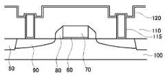
도 1에 도시한 바와 같이, 소자 분리막(50) 및 고농도 접합 영역(90)이 형성된 반도체 기판(100) 위에 게이트 절연막(60) 및 게이트 전극(70)이 차례로 형성되어 있고, 게이트 절연막(60) 및 게이트 전극(70) 측면에 스페이서(80)가 형성되어 있다.As shown in FIG. 1, the
그리고 반도체 기판(100), 게이트 전극(70) 및 스페이서(80) 위에 하부 비아 홀(115) 및 하부 트렌치(120)를 가지는 하부 금속간 절연막(inter-metal dielectric, IMD)(110)이 형성되어 있고, 하부 비아홀(115)과 하부 트렌치(120) 내벽에는 각각에 대응하는 하부 배리어막(125a, 125b)이 형성되어 있다.A lower inter-metal dielectric (IMD) 110 having a
하부 배리어막(125a, 125b)으로 둘러싸인 내측에는 하부 금속 배선(130a, 130b)이 각각 대응하여 형성되어 있다. 여기서, 하부 금속 배선(130a)은 텅스텐으로 구성되고, 하부 금속 배선(130b)은 구리로 구성된다. 따라서, 하부 배리어막(125a)은 텅스텐 확산 방지막으로 구성되고, 하부 배리어막(125b)는 구리 확산 방지막으로 구성되는 것이 일반적이다.
그리고, 하부 금속 배선(130b) 위에는 하부 전도성 배리어막(140)이 형성되어 있다.The lower
그리고 하부 금속간 절연막(110)과 전도성 배리어막(140) 위에 상부 비아홀(150) 및 상부 트렌치(155)를 가지는 상부 금속간 절연막(145)이 형성되어 있고, 상부 비아홀(150) 및 상부 트렌치(155) 내벽에 상부 배리어막(160)이 형성되어 있고, 상부 배리어막(160) 위에 상부 금속 배선(165)이 형성되어 있고, 상부 금속 배선(165) 위에 상부 금속간 절연막(145)의 높이와 동일한 상부 전도성 배리어막(170)이 형성되어 있다.An upper
여기서 하부 및 상부 전도성 배리어막(140, 170)은 Ti, SiN, TiN, Ru 등과 같은 전도성 금속으로 만들어지고, 하부 및 상부 배리어막(125, 160)과 하부 및 상부 전도성 배리어막(140, 170)은 각각 하부 및 상부 금속 배선(130, 165)이 하부 및 상부 금속간 절연막(110, 145)으로 확산되는 것을 방지한다.The lower and upper
하부 및 상부 금속간 절연막(110, 145)은 저유전율을 가지는 PSG (phosphorous silicate glass), BPSG(boron phosphorous silicate glass), FSG (fluorine doped silicate glass) 및 USG(un-doped silicate glass) 등과 같은 절연물질로 이루어질 수 있다.The lower and upper intermetallic
도 2 내지 도 5는 본 발명의 한 실시예에 따른 반도체 소자의 금속 배선을 제조 단계별로 도시한 도면이다.2 to 5 are diagrams illustrating manufacturing steps of metal wirings of a semiconductor device according to an exemplary embodiment of the present invention.
도 2 및 도 3에 도시한 바와 같이, 소자 분리막(50) 및 고농도 접합 영역(90)이 형성된 반도체 기판(100) 위에 게이트 절연막(60) 및 게이트 전극(70)을 차례로 형성하고, 게이트 절연막(60) 및 게이트 전극(70) 측면에 스페이서(80)를 형성한다.2 and 3, the
다음, 반도체 기판(100), 게이트 전극(70) 및 스페이서(80) 위에 하부 금속간 절연막(110)을 형성하고 하부 금속간 절연막(110) 위에 감광막을 사용하여 하부 비아홀 패턴(도시하지 않음)을 형성한다.Next, a lower intermetallic
다음, 상기 감광막으로 이루어진 비아홀 패턴을 마스크로 사용하여 하부 금속간 절연막(110)을 식각함으로써 반도체 기판(100)을 노출하는 하부 비아홀(115)을 형성한다.Next, a
그 다음, 하부 배리어막(125a)을 형성하고 하부 금속 배선막(130a)를 형성한다. 그 다음, 하부 금속간 절연막(110)을 추가로 증착하고 패터닝하여 하부 트렌치(120)을 형성한다.Next, the
그 다음, 하부 트렌치(120)에 하부 배리어 금속막(127)을 형성한다.Next, a lower
하부 배리어 금속막(127)은 화학 기상 증착(chemical vapor deposition, CVD), 물리적 증착(physical vapor deposition, PVD) 또는 원자층 증착(atomic layer deposition, ALD)과 같은 방법에 의하여 형성 가능하다.The lower
그 다음, 도 4에 도시한 바와 같이, 화학 기계적 연마(chemical mechanism polishing) 공정을 진행한다. 화학 기계적 연마 공정은 기판(100)의 상부 표면 전체에 대하여 이루어진다. 상기 화학 기계적 연마 공정에 의하여 하부 금속층(135)과 하부 배리어 금속막(127)이 제거된다.Next, as shown in FIG. 4, a chemical mechanical polishing process is performed. The chemical mechanical polishing process is performed over the entire upper surface of the
본 발명의 화학 기계적 연마 공정에서는 하부 배리어 금속막(127)보다 하부 금속층(135)에 대한 식각 선택비가 높은 슬러리(slurry)를 사용하는 것이 바람직하다.In the chemical mechanical polishing process of the present invention, it is preferable to use a slurry having a higher etching selectivity with respect to the
따라서, 화학 기계적 연마 공정을 마친 하부 금속 배선(130)의 상부 표면 높이는하부 금속간 절연막(110)의 상부 표면의 높이보다 보다 낮게 형성된다.Therefore, the height of the upper surface of the
한편, 이와 같이 하부 금속 배선(130)을 하부 금속간 절연막(110)의 높이보 다 낮게 만드는 공정은 상기 화학 기계적 연마 공정을 진행한 다음 소정의 마스크 패턴을 사용하여 하부 금속 배선(130)에 습식 식각(wet etch)을 진행하는 공정으로 대체 가능할 것이다.Meanwhile, the process of making the
그 다음, 도 4에 도시된 바와 같이, 하부 금속 배선(130) 위에 하부 금속간 절연막(110)의 높이과 일치 하는 하부 전도성 배리어막(140)을 형성한다.Next, as shown in FIG. 4, a lower
이때, 하부 전도성 배리어막(140)은 Ti, SiN, TiN, Ru 등과 같은 전도성 금속으로 만들어질 수 있다.In this case, the lower
이와 같이 하부 전도성 배리어막(140)을 하부 금속 배선(130) 위에만 존재하도록 만듦으로써 종래에 금속간 절연막 위에 전체적으로 존재하는 전도성 배리어막으로 인해 하부 금속간 절연막의 유전율(effective k)이 높아지는 것을 방지하여 반도체 소자의 신뢰성을 향상시킬 수 있다.As such, by making the lower
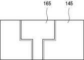
그런 다음, 도 5에 도시한 바와 같이, 하부 금속간 절연막(110) 및 하부 전 도성 배리어막(140) 위에 상부 금속간 절연막(145)을 형성한다.Next, as shown in FIG. 5, an upper intermetallic insulating
다음, 상부 금속간 절연막(145) 위에 감광막을 사용하여 상부 비아홀 패턴(도시하지 않음)을 형성하고 이를 마스크로 삼아 상부 금속간 절연막(145)을 식각하여 하부 전도성 배리어막(140)을 노출하는 상부 비아홀(150)을 형성한다.Next, an upper via hole pattern (not shown) is formed on the upper intermetallic insulating
그리고 상부 금속간 절연막(145) 위에 감광막을 사용한 상부 트렌치 패턴(도시하지 않음)을 형성하고 이를 마스크로 하여 상부 금속간 절연막(145)의 상부를 일정 두께로 제거하는 리세스(recess) 공정을 수행하여 상부 트렌치(155)를 형성한다.In addition, an upper trench pattern (not shown) using a photoresist film is formed on the upper intermetallic insulating
그 다음, 상부 비아홀(150)에 노출된 하부 전도성 배리어막(140)을 제거한다. 이때, 상부 비아홀(150)을 통하여 노출된 하부 전도성 배리어막(140)은 제거되지 않을 수도 있다.Next, the lower
하부 전도성 배리어막(140)은 반도체 소자를 제조하는 공정 진행시 발생하는 열에 의해 하부 금속 배선(130)이 상부 금속간 절연막(145)으로 확산되는 것을 방지한다. 그 결과, RC 지연의 발생을 방지할 수 있다는 이점이 있다.The lower
이어, 상부 비아홀(150) 및 상부 트렌치(155)를 갖는 상부 금속간 절연막 (145) 위에 상부 배리어 금속막(167)과 상부 금속층(175)을 형성한다.Next, an upper
이때, 상부 금속층(175)은 구리로 이루어지는 것이 바람직하다.At this time, the
그 다음, 도 6에 도시한 바와 같이, 화학 기계적 연마(chemical mechanism polishing) 공정을 진행하여 상부 금속간 절연막(145) 위에 존재하는 상부 배리어 금속막(167) 및 상부 금속층(175)을 제거하여 상부 배리어막(160) 및 상부 금속 배선(165)을 형성한다.Next, as shown in FIG. 6, a chemical mechanical polishing process is performed to remove the upper
이때, 화학 기계적 연마 공정에서는 상부 배리어 금속막(167)보다 상부 금속 층(175)에 대한 식각 선택비가 높은 슬러리(slurry)를 사용한다.In this case, in the chemical mechanical polishing process, a slurry having a higher etching selectivity with respect to the
따라서 화학 기계적 연마 공정을 마친 상부 금속 배선(165)의 상부 표면의 높이는 상부 금속간 절연막(145)의 상부 표면의 높이보다 낮게 형성된다.Therefore, the height of the upper surface of the
그러나 이와 같이 상부 금속 배선(165)을 상부 금속간 절연막(145)의 높이보다 낮게 만드는 공정은 화학 기계적 연마 공정을 진행하고 소정의 마스크 패턴을 사용하여 상부 금속 배선(165)에 습식 식각(wet etch)을 진행하는 공정 단계로 이루어질 수 있다.However, the process of making the
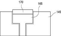
그런 다음, 도 1에 도시한 바와 같이, 상부 금속 배선(165) 위에 상부 전도 성 배리어막(170)을 형성한다.Then, as shown in FIG. 1, the upper
이때, 상부 전도성 배리어막(170)은 Ti, SiN, TiN, Ru 등과 같은 전도성 금속으로 만들어질 수 있다.In this case, the upper
이와 같이 상부 전도성 배리어막(170)을 상부 금속 배선(165) 위에만 존재하 도록 만듦으로써 종래에 금속간 절연막 위에 전체적으로 존재하는 전도성 배리어막 으로 인해 상부 금속간 절연막의 유효 유전율(effective k)이 높아지는 것을 방지하여 RC 지연을 방지함으로써 반도체 소자의 신뢰성을 향상시킬 수 있다.As such, by making the upper
한편, 도 7a 내지 7d는 도 1에서 설명한 상부 전도성 배리어막(170)의 형성 방법을 설명하는 공정도가 구체적으로 도시되어 있다. 그리고, 도 8a 및 8b에는 도 1에서 설명한 상부 전도성 배리어막(170)의 또 다른 형성 방법을 설명하는 공정도가 구체적으로 도시되어 있다.7A to 7D are detailed flowcharts illustrating a method of forming the upper
참고로, 도 7a~도 7d, 도 8a, 및 도 8b에 도시된 상부 전도성 배리어막(170)의 형성 방법은 도 4에서 설명한 하부 전도성 배리어막(170)의 형성 방법에도 동일하게 적용할 수 있다.For reference, the method of forming the upper
먼저, 도 7a 및 도 7b에 도시된 바와 같이, 화학 기계적 연마 공정에 의하여 상부 금속 배선(165)의 상부 표면의 높이는 상부 금속간 절연막(145)의 상부 표면의 높이보다 낮게 형성된다. 이렇게 되는 이유는 전술한 바와 같이 상기 화학 기계적 연마 공정의 경우 상부 배리어 금속막(167)보다 상부 금속 층(175)에 대한 식각 선택비가 높은 슬러리(slurry)를 사용하기 때문이다.First, as shown in FIGS. 7A and 7B, the height of the upper surface of the
다음, 도 7c에 도시된 바와 같이, 기판의 전면에 대하여 상부 전도상 배리어막(170)을 형성한다.Next, as shown in FIG. 7C, the upper conductive
그 다음, 도 7d에 도시된 바와 같이, 화학 기계적 연마 공정을 수행하여 상부 금속간 절연막(145)이 노출시킨다.Next, as shown in FIG. 7D, a chemical mechanical polishing process is performed to expose the upper intermetallic insulating
따라서, 도 1에서 설명한 바와 같은 상부 전도상 배리어막(170)이 형성된다.Thus, the upper conductive
그런데, 도 7a~도 7d의 방법을 사용하여 상부 전도상 배리어막(170)을 형성 하는 경우, CMP 공정에 의하여 초래되는 디싱(dishing) 현상으로 인하여 여 상부 전도상 배리어막(170)의 두께가 균일하지 않다는 문제점이 초래될 가능성이 있다. 이는 RC 지연 등의 문제를 초래할 가능성이 있다.However, when the upper conductive
이에 본 발명에서는 또 다른 방법을 제안한다.Accordingly, the present invention proposes another method.
도 8a와 도 8b에는 상부 전도성 배리어막(170)을 형성하기 위한 또 다른 형성 방법의 공정도가 도시되어 있다.8A and 8B show process diagrams of another forming method for forming the upper
도 8a는 도 7c에 대응하는 도면으로 상부 전도성 배리어막(170)이 형성되어 있는 상태도이다.FIG. 8A is a view corresponding to FIG. 7C and illustrates a state in which the upper
본 발명에서는 CMP 공정에 의한 디싱 형상을 제거하기 위하여, 도 8b에 도시된 바와 같은 감광제 패턴(181)을 형성한다.In the present invention, in order to remove the dishing by the CMP process, a
다음, 도 8c에 도시된 바와 같이, 감광제 패턴(181)을 마스크로 이용하여 감광제가 도포되어 있지 않은 상부 전도성 배리어막(170)을 전체적으로 식각하여 제거한다. 그 후, 감광제 패턴(181)을 제거한다.Next, as illustrated in FIG. 8C, the upper
도 8c에 도시된 바와같이, 감광제 패턴을 사용하는 경우, 상부 전도성 배리어막(170)의 두께가 균일하게 유지됨을 알 수 있다(도 7c, 7d와 달리, 상부 전도성 배리어막(170)의 상부 표면의 높이는 상부 금속간 절연막(145)의 상부 표면 높이 보다 더 높게 형성된다).As shown in FIG. 8C, when the photoresist pattern is used, it can be seen that the thickness of the upper
따라서, 패드와의 와이어 연결시 RC 지연이 증가할 가능성이 줄어든다. 따라서, 반도체 소자의 신뢰성이 전체적으로 개선되는 효과가 있다.Therefore, the possibility of increasing the RC delay in the wire connection with the pad is reduced. Therefore, there is an effect that the overall reliability of the semiconductor device is improved.
본 발명에 따르면 다마신 공정에서 하부 금속 배선이 상부 금속간 절연막으로 확산되는 것을 방지하기 위해 하부 금속 배선 위에만 전도성 배리어막을 만듦으로써 하부 전도성 배리어막이 하부 금속 배선을 둘러싼 하부 금속간 절연막의 유전율 변화에 영향을 미치지 않게 하고 금속 배선의 저항을 감소시켜 반도체 소자의 특성 및 신뢰성을 향상시킨다.According to the present invention, in order to prevent the lower metal interconnection from diffusing into the upper intermetallic insulation layer in the damascene process, a conductive barrier layer is formed only on the lower metal interconnection so that the lower conductive barrier layer is used to change the dielectric constant of the lower intermetallic insulation layer surrounding the lower metal interconnection. It improves the characteristics and reliability of the semiconductor device by reducing the resistance of the metal wires without affecting.
또한, 본 발명에서 제안한 상부 또는 하부 전도성 배리어막을 형성하는 공정 과정에 의하면, 구리로 이루어진 금속 배선 상부에 전도성 배리어막을 안정적으로 형성할 수 있다는 이점이 있다. 그 결과 반도체 소자의 신뢰성이 상승하는 효과를 얻을 수 있다.In addition, according to the process of forming the upper or lower conductive barrier film proposed in the present invention, there is an advantage that the conductive barrier film can be stably formed on the metal wiring made of copper. As a result, the reliability of the semiconductor element can be obtained.
한편, 본 발명의 바람직한 실시예에 대하여 상세하게 설명하였지만, 당해 기술 분야에서 통상의 지식을 가진 자라면 이로부터 다양한 변형 및 균등한 타 실시예가 가능하다는 점을 이해할 수 있을 것이다.Meanwhile, although preferred embodiments of the present invention have been described in detail, those skilled in the art will appreciate that various modifications and equivalent other embodiments are possible therefrom.
따라서, 본 발명의 권리 범위는 이에 한정되는 것은 아니고 다음의 청구범위에서 정의하고 있는 본 발명의 기본 개념을 이용한 당업자의 여러 변형 및 개량 형태 또한 본 발명의 권리범위에 속한다고 보아야 한다.Accordingly, the scope of the present invention is not limited thereto, and various modifications and improvements of those skilled in the art using the basic concept of the present invention defined in the following claims should also be considered to belong to the scope of the present invention.
Claims (9)
Translated fromKoreanPriority Applications (3)
| Application Number | Priority Date | Filing Date | Title |
|---|---|---|---|
| KR1020060135767AKR20080061030A (en) | 2006-12-27 | 2006-12-27 | Metal wiring formation method of semiconductor device |
| US11/986,588US20080157380A1 (en) | 2006-12-27 | 2007-11-23 | Method for forming metal interconnection of semiconductor device |
| CNA2007103081104ACN101211824A (en) | 2006-12-27 | 2007-12-27 | Method for forming metal interconnection of semiconductor device and semiconductor device |
Applications Claiming Priority (1)
| Application Number | Priority Date | Filing Date | Title |
|---|---|---|---|
| KR1020060135767AKR20080061030A (en) | 2006-12-27 | 2006-12-27 | Metal wiring formation method of semiconductor device |
Publications (1)
| Publication Number | Publication Date |
|---|---|
| KR20080061030Atrue KR20080061030A (en) | 2008-07-02 |
Family
ID=39582754
Family Applications (1)
| Application Number | Title | Priority Date | Filing Date |
|---|---|---|---|
| KR1020060135767ACeasedKR20080061030A (en) | 2006-12-27 | 2006-12-27 | Metal wiring formation method of semiconductor device |
Country Status (3)
| Country | Link |
|---|---|
| US (1) | US20080157380A1 (en) |
| KR (1) | KR20080061030A (en) |
| CN (1) | CN101211824A (en) |
Cited By (1)
| Publication number | Priority date | Publication date | Assignee | Title |
|---|---|---|---|---|
| US8828865B2 (en) | 2011-03-28 | 2014-09-09 | Samsung Electronics Co., Ltd. | Method of forming metal interconnections of semiconductor device |
Families Citing this family (19)
| Publication number | Priority date | Publication date | Assignee | Title |
|---|---|---|---|---|
| KR101016505B1 (en)* | 2008-09-11 | 2011-02-24 | 주식회사 동부하이텍 | Image sensor and manufacturing method |
| US8669644B2 (en)* | 2009-10-07 | 2014-03-11 | Texas Instruments Incorporated | Hydrogen passivation of integrated circuits |
| US8610275B2 (en) | 2010-07-14 | 2013-12-17 | Institute of Microelectronics, Chinese Academy of Sciences | Semiconductor contact structure including a spacer formed within a via and method of manufacturing the same |
| CN102339813A (en)* | 2010-07-14 | 2012-02-01 | 中国科学院微电子研究所 | Semiconductor structure and manufacturing method thereof |
| US20120142177A1 (en)* | 2010-12-03 | 2012-06-07 | Jee-Yong Kim | Methods of manufacturing a wiring structure and methods of manufacturing a semiconductor device |
| CN102543942A (en)* | 2010-12-08 | 2012-07-04 | 和舰科技(苏州)有限公司 | Integrated circuit dielectric layer structure containing stop layer |
| KR101789765B1 (en) | 2010-12-16 | 2017-11-21 | 삼성전자주식회사 | Semiconductor device and method of forming the same |
| JP5853389B2 (en)* | 2011-03-28 | 2016-02-09 | ソニー株式会社 | Semiconductor device and manufacturing method of semiconductor device. |
| CN103021929A (en)* | 2011-09-22 | 2013-04-03 | 中芯国际集成电路制造(北京)有限公司 | Manufacturing method of semiconductor device |
| CN103021931B (en)* | 2011-09-23 | 2015-09-23 | 北京泰龙电子技术有限公司 | Preparation method of metal nitride barrier layer |
| CN103545247B (en)* | 2012-07-13 | 2016-08-03 | 中芯国际集成电路制造(上海)有限公司 | Metal closures preparation method and the application in phase-change random access memory thereof |
| CN104183575B (en)* | 2013-05-21 | 2018-05-08 | 中芯国际集成电路制造(上海)有限公司 | A kind of semiconductor devices and preparation method thereof |
| US9837350B2 (en) | 2016-04-12 | 2017-12-05 | International Business Machines Corporation | Semiconductor interconnect structure with double conductors |
| US10134580B1 (en)* | 2017-08-15 | 2018-11-20 | Globalfoundries Inc. | Metallization levels and methods of making thereof |
| US10510657B2 (en)* | 2017-09-26 | 2019-12-17 | Taiwan Semiconductor Manufacturing Co., Ltd. | Semiconductor device with interconnecting structure and method for manufacturing the same |
| US10319629B1 (en)* | 2018-05-08 | 2019-06-11 | International Business Machines Corporation | Skip via for metal interconnects |
| US11694958B2 (en)* | 2020-06-03 | 2023-07-04 | International Business Machines Corporation | Layout design for threshold voltage tuning |
| KR20220092702A (en) | 2020-12-24 | 2022-07-04 | 삼성전자주식회사 | Semiconductor device |
| US12213306B2 (en)* | 2022-07-21 | 2025-01-28 | Nanya Technology Corporation | Semiconductor device with air gap and method for preparing the same |
Family Cites Families (12)
| Publication number | Priority date | Publication date | Assignee | Title |
|---|---|---|---|---|
| CA2082771C (en)* | 1992-11-12 | 1998-02-10 | Vu Quoc Ho | Method for forming interconnect structures for integrated circuits |
| US5677244A (en)* | 1996-05-20 | 1997-10-14 | Motorola, Inc. | Method of alloying an interconnect structure with copper |
| US6181012B1 (en)* | 1998-04-27 | 2001-01-30 | International Business Machines Corporation | Copper interconnection structure incorporating a metal seed layer |
| US6815336B1 (en)* | 1998-09-25 | 2004-11-09 | Taiwan Semiconductor Manufacturing Company, Ltd. | Planarization of copper damascene using reverse current electroplating and chemical mechanical polishing |
| US6258713B1 (en)* | 1999-12-03 | 2001-07-10 | United Microelectronics Corp. | Method for forming dual damascene structure |
| US6403465B1 (en)* | 1999-12-28 | 2002-06-11 | Taiwan Semiconductor Manufacturing Company | Method to improve copper barrier properties |
| US6207552B1 (en)* | 2000-02-01 | 2001-03-27 | Advanced Micro Devices, Inc. | Forming and filling a recess in interconnect for encapsulation to minimize electromigration |
| US7008872B2 (en)* | 2002-05-03 | 2006-03-07 | Intel Corporation | Use of conductive electrolessly deposited etch stop layers, liner layers and via plugs in interconnect structures |
| KR100641502B1 (en)* | 2002-12-30 | 2006-10-31 | 동부일렉트로닉스 주식회사 | Contact formation method using dual damascene process in semiconductor device manufacturing |
| US6927113B1 (en)* | 2003-05-23 | 2005-08-09 | Advanced Micro Devices | Semiconductor component and method of manufacture |
| JP4230334B2 (en)* | 2003-10-31 | 2009-02-25 | 富士通マイクロエレクトロニクス株式会社 | Semiconductor device and manufacturing method thereof |
| US7157380B2 (en)* | 2003-12-24 | 2007-01-02 | Intel Corporation | Damascene process for fabricating interconnect layers in an integrated circuit |
- 2006
- 2006-12-27KRKR1020060135767Apatent/KR20080061030A/ennot_activeCeased
- 2007
- 2007-11-23USUS11/986,588patent/US20080157380A1/ennot_activeAbandoned
- 2007-12-27CNCNA2007103081104Apatent/CN101211824A/enactivePending
Cited By (2)
| Publication number | Priority date | Publication date | Assignee | Title |
|---|---|---|---|---|
| US8828865B2 (en) | 2011-03-28 | 2014-09-09 | Samsung Electronics Co., Ltd. | Method of forming metal interconnections of semiconductor device |
| US9257389B2 (en) | 2011-03-28 | 2016-02-09 | Samsung Electronics Co., Ltd. | Semiconductor device having metal interconnections |
Also Published As
| Publication number | Publication date |
|---|---|
| CN101211824A (en) | 2008-07-02 |
| US20080157380A1 (en) | 2008-07-03 |
Similar Documents
| Publication | Publication Date | Title |
|---|---|---|
| KR20080061030A (en) | Metal wiring formation method of semiconductor device | |
| KR100729126B1 (en) | Metal wiring of semiconductor device and method of forming the same | |
| CN101390203B (en) | Interconnect structure and manufacturing method thereof | |
| JP4118029B2 (en) | Semiconductor integrated circuit device and manufacturing method thereof | |
| JP3672752B2 (en) | Dual damascene structure and method for forming the same | |
| JP5285612B2 (en) | Semiconductor device and method of forming interconnect structure | |
| US10453794B2 (en) | Interconnect structure for semiconductor devices | |
| US8030779B2 (en) | Multi-layered metal interconnection | |
| KR100818046B1 (en) | How to Form Metal Wiring | |
| KR100857989B1 (en) | Metal line formation method of semiconductor device | |
| KR100835421B1 (en) | Metal wiring formation method of semiconductor device | |
| KR101103550B1 (en) | Metal wiring formation method of semiconductor device | |
| KR100703559B1 (en) | Semiconductor device having a dual damascene structure and method of manufacturing the same | |
| KR100711912B1 (en) | Metal wiring formation method of semiconductor device | |
| KR100713552B1 (en) | Semiconductor device and manufacturing method thereof | |
| KR100738210B1 (en) | Method of forming thin film and metal wiring in semiconductor device | |
| KR100259168B1 (en) | Structure of metal interconnection line for semiconductor device and method of forming the same | |
| KR100712813B1 (en) | Manufacturing Method of Semiconductor Device | |
| KR100641488B1 (en) | Contact manufacturing method of semiconductor device | |
| JP4967207B2 (en) | Manufacturing method of semiconductor device | |
| KR100471404B1 (en) | Method for forming metal wiring of semiconductor device using chemical mechanical polishing process | |
| KR100784105B1 (en) | Manufacturing Method of Semiconductor Device | |
| KR20010056822A (en) | Conductive line and interconnection thereof in semiconductor device and fabricating method thereof | |
| TWI223876B (en) | Method of fabricating a self-aligned contact opening and structure of interconnects and fabricating method thereof | |
| KR100712817B1 (en) | Semiconductor Device and Forming Method |
Legal Events
| Date | Code | Title | Description |
|---|---|---|---|
| A201 | Request for examination | ||
| PA0109 | Patent application | Patent event code:PA01091R01D Comment text:Patent Application Patent event date:20061227 | |
| PA0201 | Request for examination | ||
| E902 | Notification of reason for refusal | ||
| PE0902 | Notice of grounds for rejection | Comment text:Notification of reason for refusal Patent event date:20080227 Patent event code:PE09021S01D | |
| AMND | Amendment | ||
| PG1501 | Laying open of application | ||
| E601 | Decision to refuse application | ||
| PE0601 | Decision on rejection of patent | Patent event date:20080826 Comment text:Decision to Refuse Application Patent event code:PE06012S01D Patent event date:20080227 Comment text:Notification of reason for refusal Patent event code:PE06011S01I | |
| J201 | Request for trial against refusal decision | ||
| PJ0201 | Trial against decision of rejection | Patent event date:20080922 Comment text:Request for Trial against Decision on Refusal Patent event code:PJ02012R01D Patent event date:20080826 Comment text:Decision to Refuse Application Patent event code:PJ02011S01I Appeal kind category:Appeal against decision to decline refusal Decision date:20090629 Appeal identifier:2008101009568 Request date:20080922 | |
| AMND | Amendment | ||
| PB0901 | Examination by re-examination before a trial | Comment text:Amendment to Specification, etc. Patent event date:20081020 Patent event code:PB09011R02I Comment text:Request for Trial against Decision on Refusal Patent event date:20080922 Patent event code:PB09011R01I Comment text:Amendment to Specification, etc. Patent event date:20080428 Patent event code:PB09011R02I | |
| B601 | Maintenance of original decision after re-examination before a trial | ||
| PB0601 | Maintenance of original decision after re-examination before a trial | ||
| J301 | Trial decision | Free format text:TRIAL DECISION FOR APPEAL AGAINST DECISION TO DECLINE REFUSAL REQUESTED 20080922 Effective date:20090629 | |
| PJ1301 | Trial decision | Patent event code:PJ13011S01D Patent event date:20090629 Comment text:Trial Decision on Objection to Decision on Refusal Appeal kind category:Appeal against decision to decline refusal Request date:20080922 Decision date:20090629 Appeal identifier:2008101009568 |