KR20080060486A - Flash memory and manufacturing method thereof - Google Patents
Flash memory and manufacturing method thereofDownload PDFInfo
- Publication number
- KR20080060486A KR20080060486AKR1020060134644AKR20060134644AKR20080060486AKR 20080060486 AKR20080060486 AKR 20080060486AKR 1020060134644 AKR1020060134644 AKR 1020060134644AKR 20060134644 AKR20060134644 AKR 20060134644AKR 20080060486 AKR20080060486 AKR 20080060486A
- Authority
- KR
- South Korea
- Prior art keywords
- film
- oxide film
- substrate
- high temperature
- forming
- Prior art date
- Legal status (The legal status is an assumption and is not a legal conclusion. Google has not performed a legal analysis and makes no representation as to the accuracy of the status listed.)
- Ceased
Links
- 238000004519manufacturing processMethods0.000titleclaimsabstractdescription12
- 239000000758substrateSubstances0.000claimsabstractdescription51
- 150000004767nitridesChemical class0.000claimsabstractdescription15
- 238000002955isolationMethods0.000claimsabstractdescription13
- 125000006850spacer groupChemical group0.000claimsabstractdescription11
- 238000005530etchingMethods0.000claimsabstractdescription6
- 238000000034methodMethods0.000claimsdescription19
- 238000004518low pressure chemical vapour depositionMethods0.000claimsdescription4
- 239000010410layerSubstances0.000description29
- 229910021420polycrystalline siliconInorganic materials0.000description20
- 229920005591polysiliconPolymers0.000description20
- 230000002093peripheral effectEffects0.000description9
- 239000000463materialSubstances0.000description5
- 238000000151depositionMethods0.000description4
- 238000000059patterningMethods0.000description4
- BOTDANWDWHJENH-UHFFFAOYSA-NTetraethyl orthosilicateChemical compoundCCO[Si](OCC)(OCC)OCCBOTDANWDWHJENH-UHFFFAOYSA-N0.000description3
- 239000012535impuritySubstances0.000description3
- 238000005468ion implantationMethods0.000description3
- 230000014759maintenance of locationEffects0.000description3
- 230000015572biosynthetic processEffects0.000description2
- 230000001351cycling effectEffects0.000description2
- 239000011810insulating materialSubstances0.000description2
- 238000001020plasma etchingMethods0.000description2
- -1spacer nitrideChemical class0.000description2
- 238000000137annealingMethods0.000description1
- 238000013500data storageMethods0.000description1
- 238000010586diagramMethods0.000description1
- 239000002019doping agentSubstances0.000description1
- 230000000694effectsEffects0.000description1
- 238000005516engineering processMethods0.000description1
- 230000006870functionEffects0.000description1
- 239000011229interlayerSubstances0.000description1
- 239000012528membraneSubstances0.000description1
- 238000012986modificationMethods0.000description1
- 230000004048modificationEffects0.000description1
- 238000003860storageMethods0.000description1
- 238000007740vapor depositionMethods0.000description1
Images


Classifications
- H—ELECTRICITY
- H10—SEMICONDUCTOR DEVICES; ELECTRIC SOLID-STATE DEVICES NOT OTHERWISE PROVIDED FOR
- H10B—ELECTRONIC MEMORY DEVICES
- H10B41/00—Electrically erasable-and-programmable ROM [EEPROM] devices comprising floating gates
- H10B41/40—Electrically erasable-and-programmable ROM [EEPROM] devices comprising floating gates characterised by the peripheral circuit region
- H—ELECTRICITY
- H10—SEMICONDUCTOR DEVICES; ELECTRIC SOLID-STATE DEVICES NOT OTHERWISE PROVIDED FOR
- H10D—INORGANIC ELECTRIC SEMICONDUCTOR DEVICES
- H10D30/00—Field-effect transistors [FET]
- H10D30/60—Insulated-gate field-effect transistors [IGFET]
- H10D30/68—Floating-gate IGFETs
- H10D30/681—Floating-gate IGFETs having only two programming levels
- H—ELECTRICITY
- H10—SEMICONDUCTOR DEVICES; ELECTRIC SOLID-STATE DEVICES NOT OTHERWISE PROVIDED FOR
- H10B—ELECTRONIC MEMORY DEVICES
- H10B41/00—Electrically erasable-and-programmable ROM [EEPROM] devices comprising floating gates
- H10B41/40—Electrically erasable-and-programmable ROM [EEPROM] devices comprising floating gates characterised by the peripheral circuit region
- H10B41/42—Simultaneous manufacture of periphery and memory cells
- H10B41/43—Simultaneous manufacture of periphery and memory cells comprising only one type of peripheral transistor
- H10B41/48—Simultaneous manufacture of periphery and memory cells comprising only one type of peripheral transistor with a tunnel dielectric layer also being used as part of the peripheral transistor
- H—ELECTRICITY
- H10—SEMICONDUCTOR DEVICES; ELECTRIC SOLID-STATE DEVICES NOT OTHERWISE PROVIDED FOR
- H10D—INORGANIC ELECTRIC SEMICONDUCTOR DEVICES
- H10D30/00—Field-effect transistors [FET]
- H10D30/60—Insulated-gate field-effect transistors [IGFET]
- H—ELECTRICITY
- H10—SEMICONDUCTOR DEVICES; ELECTRIC SOLID-STATE DEVICES NOT OTHERWISE PROVIDED FOR
- H10D—INORGANIC ELECTRIC SEMICONDUCTOR DEVICES
- H10D30/00—Field-effect transistors [FET]
- H10D30/60—Insulated-gate field-effect transistors [IGFET]
- H10D30/68—Floating-gate IGFETs
- H10D30/6891—Floating-gate IGFETs characterised by the shapes, relative sizes or dispositions of the floating gate electrode
- H—ELECTRICITY
- H10—SEMICONDUCTOR DEVICES; ELECTRIC SOLID-STATE DEVICES NOT OTHERWISE PROVIDED FOR
- H10D—INORGANIC ELECTRIC SEMICONDUCTOR DEVICES
- H10D64/00—Electrodes of devices having potential barriers
- H10D64/01—Manufacture or treatment
- H10D64/021—Manufacture or treatment using multiple gate spacer layers, e.g. bilayered sidewall spacers
- H—ELECTRICITY
- H10—SEMICONDUCTOR DEVICES; ELECTRIC SOLID-STATE DEVICES NOT OTHERWISE PROVIDED FOR
- H10D—INORGANIC ELECTRIC SEMICONDUCTOR DEVICES
- H10D64/00—Electrodes of devices having potential barriers
- H10D64/60—Electrodes characterised by their materials
- H10D64/66—Electrodes having a conductor capacitively coupled to a semiconductor by an insulator, e.g. MIS electrodes
- H10D64/68—Electrodes having a conductor capacitively coupled to a semiconductor by an insulator, e.g. MIS electrodes characterised by the insulator, e.g. by the gate insulator
- H10D64/681—Electrodes having a conductor capacitively coupled to a semiconductor by an insulator, e.g. MIS electrodes characterised by the insulator, e.g. by the gate insulator having a compositional variation, e.g. multilayered
- H10D64/685—Electrodes having a conductor capacitively coupled to a semiconductor by an insulator, e.g. MIS electrodes characterised by the insulator, e.g. by the gate insulator having a compositional variation, e.g. multilayered being perpendicular to the channel plane
- H—ELECTRICITY
- H10—SEMICONDUCTOR DEVICES; ELECTRIC SOLID-STATE DEVICES NOT OTHERWISE PROVIDED FOR
- H10D—INORGANIC ELECTRIC SEMICONDUCTOR DEVICES
- H10D84/00—Integrated devices formed in or on semiconductor substrates that comprise only semiconducting layers, e.g. on Si wafers or on GaAs-on-Si wafers
- H10D84/80—Integrated devices formed in or on semiconductor substrates that comprise only semiconducting layers, e.g. on Si wafers or on GaAs-on-Si wafers characterised by the integration of at least one component covered by groups H10D12/00 or H10D30/00, e.g. integration of IGFETs
Landscapes
- Engineering & Computer Science (AREA)
- Manufacturing & Machinery (AREA)
- Semiconductor Memories (AREA)
- Non-Volatile Memory (AREA)
Abstract
Translated fromKoreanDescription
Translated fromKorean도 1 내지 도 8는 본 발명의 플래시 메모리의 제조 공정을 도시한 도이다.1 to 8 are diagrams illustrating a manufacturing process of the flash memory of the present invention.
본 발명은 플래시 메모리 및 그 제조 방법에 관한 것이다.The present invention relates to a flash memory and a method of manufacturing the same.
플래시 메모리는 전원이 꺼지더라도 저장된 데이터가 손상되지 않는 비휘발성 기억매체이면서도 데이터의 기록, 읽기, 삭제 등의 처리 속도가 비교적 높다는 장점이 있다. 이에 따라, 상기 플래시 메모리는 PC의 Bios용, 셋탑 박스, 프린터 및 네트워크 서버 등의 데이터 저장용으로 널리 사용되고 있으며 최근에는 디지털 카메라와 휴대폰 등에서도 많이 이용되고 있다.Flash memory is a nonvolatile storage medium that does not damage stored data even when the power is turned off, but has a relatively high processing speed for writing, reading, and deleting data. Accordingly, the flash memory is widely used for data storage of a PC bios, a set-top box, a printer, and a network server. Recently, the flash memory is also widely used in digital cameras and mobile phones.
이러한 플래시 메모리는 사이클링(Cycling) 및 데이터 리텐션(Data Retention) 특성이 매우 중요하다. 사이클링이란 플래시 메모리에서 가장 중요한 특성으로 데이터를 읽고, 쓰고, 소거하는 것을 여러 번 반복해도 특성의 변화없이 일정한 전자를 플로팅 게이트 안에 넣고 빼고를 반복하는 것을 말한다. 데이터 리텐션이란 플로팅 게이트에 있는 전자들이 오엔오(ONO) 및 터널 산화막을 통해 빠져나가는 것을 말하는데, 특히 셀 영역의 에지(edge) 부분을 통해 흐르는 누설 전류와 폴로팅 게이트 사이드로 빠져나가는 전자는 데이터 리텐션이 나빠지게 하는 문제점이 있다.Cycling and data retention characteristics of the flash memory are very important. Cycling is the most important characteristic of flash memory, which means that it repeats reading and writing data and erasing data several times and inserting and subtracting a constant electron into a floating gate without changing the characteristic. Data retention refers to the escape of electrons in the floating gate through the ONO and tunnel oxide layers, especially the leakage current flowing through the edge of the cell region and the electrons exiting the floating gate side. There is a problem of poor retention.
또한, 기술이 계속적으로 발전하면서 0.18㎛급 이상에서 생기지 않던 문제가 0.13㎛로 내려오면서 생기기 시작하는데, 그 중 하나가 게이트와 콘택홀이 가까워지면서 플로팅 게이트 주변에 있던 전하들이 후속 공정을 거치면서도 없어지지 않는 현상이 발생하고 있다.In addition, as technology continues to develop, problems that do not occur above 0.18µm begin to occur as they descend to 0.13µm, one of which is closer to the gate and the contact hole, so that the charges around the floating gate do not disappear through subsequent processes. Is not happening.
본 발명은 상기한 바와 같은 종래의 문제점을 개선하기 위한 것으로서, 플래시 메모리의 플로팅 게이트에 저장되어 있는 전자가 주변으로 빠져나가는 것을 방지하고, 또한 스페이서 질화막에 있는 전자들이 플로팅 게이트로 들어오는 것을 방지하여 플래시 메모리의 전기적 특성을 향상시킬 수 있는 플래시 메모리 및 그 제조 방법을 제공하는 데 있다.SUMMARY OF THE INVENTION The present invention is to improve the above-described problems, and prevents electrons stored in the floating gate of the flash memory from escaping to the surroundings and prevents electrons in the spacer nitride film from entering the floating gate. It is to provide a flash memory and a method of manufacturing the same that can improve the electrical characteristics of the memory.
본 발명에 따른 플래시 메모리 제조 방법은,Flash memory manufacturing method according to the present invention,
기판에 소자 분리막을 형성하는 단계; 상기 기판 위에 터널 산화막과 플로팅 게이트를 형성하는 단계; 상기 기판 전면에 오엔오막(ONO)을 형성하는 단계; 상기 오엔오막 위에 제어 게이트를 형성하는 단계; 상기 제어 게이트가 형성된 기판 전면에 고온 산화막을 형성하고, 상기 고온 산화막 위에 질화막을 형성하는 단계; 및, 상기 고온 산화막과 질화막을 식각하여 스페이서를 형성하는 단계를 포함한다.Forming an isolation layer on the substrate; Forming a tunnel oxide film and a floating gate on the substrate; Forming an ONO film on the entire surface of the substrate; Forming a control gate on the ohio film; Forming a high temperature oxide film on an entire surface of the substrate on which the control gate is formed, and forming a nitride film on the high temperature oxide film; And etching the high temperature oxide film and the nitride film to form a spacer.
또한, 본 발명에 따른 플래시 메모리는,In addition, the flash memory according to the present invention,
소자 분리막이 형성된 기판; 상기 기판 위에 형성된 터널 산화막과 플로팅 게이트; 상기 플로팅 게이트 위에 형성된 오엔오막; 상기 오엔오막 위에 형성된 제어 게이트; 및, 상기 터널 산화막, 플로팅 게이트, 오엔오막, 제어 게이트의 측면에 형성되고, 고온 산화막과 질화막으로 이루어진 스페이서를 포함한다.A substrate on which an isolation layer is formed; A tunnel oxide film and a floating gate formed on the substrate; An ohon layer formed on the floating gate; A control gate formed on the ohio film; And a spacer formed on a side surface of the tunnel oxide film, the floating gate, the ohio film, and the control gate, and formed of a high temperature oxide film and a nitride film.
이하, 첨부된 도면을 참조하여 본 발명의 실시예를 상세히 설명한다. 우선, 도면들 중 동일한 구성요소 또는 부품들은 가능한 한 동일한 참조부호를 나타내고 있음에 유의해야 한다. 본 발명을 설명함에 있어서 관련된 공지기능 혹은 구성에 대한 구체적인 설명은 본 발명의 요지를 모호하게 하지 않기 위해 생략한다.Hereinafter, with reference to the accompanying drawings will be described an embodiment of the present invention; First, it should be noted that the same components or parts in the drawings represent the same reference numerals as much as possible. In describing the present invention, detailed descriptions of related well-known functions or configurations are omitted in order not to obscure the gist of the present invention.
또한, 본 발명에 따른 실시 예의 설명에 있어서, 각 층(막), 영역, 패턴 또는 구조물들이 기판, 각 층(막), 영역, 패드 또는 패턴들의 "위(on/above/over/upper)"에 또는 "아래(down/below/under/lower)"에 형성되는 것으로 기재되는 경우에 있어, 그 의미는 각 층(막), 영역, 패드, 패턴 또는 구조물들이 직접 기판, 각 층(막), 영역, 패드 또는 패턴들에 접촉되어 형성되는 경우로 해석될 수도 있으며, 다른 층(막), 다른 영역, 다른 패드, 다른 패턴 또는 다른 구조물들이 그 사이에 추가적으로 형성되는 경우로 해석될 수도 있다. 따라서, 그 의미는 발명의 기술적 사상에 의하여 판단되어야 한다.In addition, in the description of an embodiment according to the present invention, each layer (film), region, pattern or structure is "on / above / over / upper" of the substrate, each layer (film), region, pad or patterns. In the case where it is described as being formed at or "down / below / under / lower", the meaning is that each layer (film), area, pad, pattern or structure is a direct substrate, each layer (film), It may be interpreted as being formed in contact with an area, pad or patterns, or may be interpreted as another layer (film), another area, another pad, another pattern, or another structure being additionally formed therebetween. Therefore, the meaning should be determined by the technical spirit of the invention.
도 1 내지 도 8는 본 발명의 플래시 메모리의 제조 공정을 나타낸 것이다.1 to 8 illustrate a manufacturing process of the flash memory of the present invention.
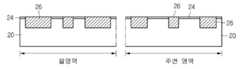
도 1에 도시한 바와 같이, 셀 영역과 주변 영역이 구획된 기판(20)이 마련되고, 상기 기판(20) 위에 산화막(21), 질화막(22), 그리고 절연막(23)을 순차적으로 형성한다. 이때, 상기 절연막(23)은 테오스막(TEOS)일 수 있다.As shown in FIG. 1, a
그 다음, 도 2에 도시한 바와 같이, 상기 절연막(23) 상에 소정의 마스크 물질을 증착한 후, 패터닝하고 이러한 마스크막을 이용하여 식각 공정을 수행하여 상기 기판(20)을 식각하고, 상기 마스크막을 제거한다.Next, as shown in FIG. 2, after depositing a predetermined mask material on the insulating film 23, the
상기 기판(20) 상에 소정의 절연 물질을 갭 필링(gap filling)한 후, 트렌치 CMP 공정을 수행하여 상기 기판(20) 상에 소자 분리막(26)을 형성한다. 상기 소자 분리막(26)은 추후 상기 기판(20) 상에 형성될 각종 소자를 절연하기 위한 영역으로 사용된다. 이때, 상기 절연 물질은 HDP-USG막일 수 있다.After gap filling a predetermined insulating material on the
이어서, 상기 질화막을 제거한다. 이에 따라, 상기 기판(20) 상에는 소자 분리막(26)과 상기 소자 분리막(26) 사이의 기판(20) 상에 산화막(24)이 형성되어 있다.Next, the nitride film is removed. Accordingly, an
도 2에 도시되지 않았지만, 상기 소자 분리막(26)을 포함한 상기 기판(20)을 대상으로 선택적으로 이온 주입 공정을 수행하여, 상기 기판(20) 상에 P 웰(well) 및 N 웰을 형성한다.Although not shown in FIG. 2, an ion implantation process is selectively performed on the
그 다음, 도 3에 도시한 바와 같이, 상기 기판(20)의 전면 상에 소정의 폴리실리콘막을 증착한 후 상기 셀 영역의 기판(20)을 대상으로 패터닝하여 제1 폴리실리콘막(28')을 형성한다. 상기 제1 폴리실리콘막(28')은 플로팅 게이트이고, 그 하부에는 산화막(24)이 패터닝되어 형성된 터널 산화막이다. 상기 제1 폴리실리콘막(28')은 산화막(24)과 ONO막(30) 사이에 고립된 상태에서 도핑물질이 내부에 도핑되어서 전하(전자)를 보유하고 여기(Excite)된 상태로 있게 된다.3, after depositing a predetermined polysilicon film on the entire surface of the
이어서, 상기 기판(20)의 전면에 옥사이드(oxide), 나이트라이드(nitride), 옥사이드(oxide)를 순차적으로 적층한 후 어닐(anneal) 공정을 수행한 다음 상기 셀 영역의 기판을 대상으로 패터닝하여 상기 제1 폴리실리콘막(28')을 둘러싸도록 ONO막(30)을 형성한다. 상기 ONO막(30)은 상/하부를 절연하는 역할을 한다.Subsequently, oxide, nitride, and oxide are sequentially stacked on the entire surface of the
이러한 경우, 상기 주변 영역의 기판(20) 상에는 상기 폴리실리콘막(28)과 ONO막(30)이 적층 형성되어 있다.In this case, the
그 다음, 도 4에 도시한 바와 같이, 상기 기판(20)의 전면에 소정의 마스크 물질을 형성하고 패터닝하여 상기 주변 영역의 마스크 물질을 제거하여 상기 셀 영역의 기판(20) 상에만 마스크막이 형성되도록 한다.Next, as shown in FIG. 4, a predetermined mask material is formed on the entire surface of the
이어서, 상기 마스크막을 이용하여 상기 기판(20)을 식각하여 상기 주변 영역의 기판(20) 상에 형성된 상기 폴리실리콘막(28)과 ONO막(30)을 제거한다.Subsequently, the
그 다음, 도 5에 도시한 바와 같이, 상기 셀 영역 및 상기 주변 영역을 포함하는 기판(20)의 전 영역에 소정의 폴리실리콘막(32)을 증착한다.Next, as shown in FIG. 5, a
상기 폴리실리콘막(32)을 증착하기 전에 상기 주변 영역의 기판(20) 상에 산화막(24)을 선택적으로 제거할 수 있다. 상기 선택 제거된 산화막(24)에 의해 상기 기판(20)이 노출된 영역으로 후술하는 이온 주입 공정에 의해 상기 기판(20)에 불순물 영역이 형성될 수 있다.Before depositing the
그 다음, 도 6에 도시한 바와 같이, 상기 폴리실리콘막(32)을 대상으로 패터닝하여 제2 폴리실리콘막(32a, 32b)을 형성한다.6, the
상기 셀 영역의 기판(20)의 제2 폴리실리콘막(32a)은 상기 ONO막(30)을 덮어 형성되고, 상기 주변 영역의 기판(20)의 제2 폴리실리콘막(32b)은 상기 소자 분리막(26) 사이, 즉 게이트 형성 영역에 형성된다. 상기 셀 영역의 기판(20)에 형성된 제2 폴리실리콘막(32a)은 제어 게이트이고, 상기 주변 영역의 기판에 형성된 제2 폴리실리콘막(32b)은 플로팅 게이트이다.The
상기 셀 영역의 기판(20)에 형성된 제2 폴리실리콘막(32a)은 하부에 있는 상기 제1 폴리실리콘막(28')에 내재된 전자를 여기시켜서 충전(charging) 혹은 방전(discharging)하기 위하여 바이어스 전압을 인가시키는 역할을 한다.The
그 다음, 도 7에 도시한 바와 같이, 상기 기판(20) 전면에 고온 산화막(41)을 형성한 후, 상기 고온 산화막(41) 위에 질화막(42)을 형성한다. 이때, 상기 고온 산화막(41)은 500 내지 800℃ 온도의 산화막일 수 있으며, 바람직하게는 상기 고온 산화막은 780℃ 온도의 산화막이다. 또한, 상기 고온 산화막은 100 내지 200Å의 두께로 형성한다. 또한, 상기 고온 산화막은 여러가지 증착법을 사용할 수 있으나, 저압 화학 기상 증착법(LP-CVD)으로 형성하는 것이 바람직하다.Next, as shown in FIG. 7, after forming the high
그 다음, 도 8에 도시한 바와 같이, 반응성 이온 식각 공정(RIE)으로 상기 고온 산화막(41)과 질화막(42)을 전면 식각하여, 상기 제2 폴리실리콘막(32a, 32b)의 측벽에 고온 산화막 패턴(41')과 질화막 패턴(42')으로 이루어진 스페이서(43)를 형성한 후, 상기 제2 폴리실리콘막(34a, 32b)과 상기 스페이서(43)를 마스크로 하여 이온 주입 공정을 수행하여 상기 기판(20) 내부에 불순물 영역(36), 즉 소스 및 드레인 영역을 형성한다.Next, as shown in FIG. 8, the high
그 다음, 상기 기판(20) 상에 PMD 물질(38)을 증착한 후, 상기 PMD 물질(38)을 선택 식각하여 콘택홀을 갖는 층간 절연막을 형성한 후, 상기 콘택홀에 컨택을 형성함으로써, 상기 콘택이 상기 주변 영역의 기판(20)의 불순물 영역(26)과 전기적으로 연결한다.Then, after depositing the PMD material 38 on the
이에 따라, 플래시 메모리의 제조가 완성될 수 있다.Accordingly, the manufacture of the flash memory can be completed.
이상에서 본 발명의 설명의 편리를 위해 일부 공정들에 대한 설명이 생략되었지만, 생략된 공정들은 일반적으로 널리 알려진 공지 기술로서, 본 발명의 사상을 크게 저해하지는 않을 것이다.Although a description of some of the processes have been omitted for the convenience of description of the present invention, the omitted processes are generally well known techniques and will not significantly impair the spirit of the present invention.
상기와 같은 방법으로 제조된 본 발명의 플래시 메모리는, 기판에는 소자 분리막이 형성되고, 상기 기판 위에는 터널 산화막과 플로팅 게이트가 형성된다.In the flash memory of the present invention manufactured by the above method, an element isolation film is formed on a substrate, and a tunnel oxide film and a floating gate are formed on the substrate.
상기 플로팅 게이트 위에는 오엔오막이 형성되고, 상기 오엔오막 위에는 제어 게이트가 형성된다.An Ohn film is formed on the floating gate, and a control gate is formed on the Oho film.
상기 터널 산화막, 플로팅 게이트, 오엔오막, 제어 게이트의 측면에는 스페 이서가 형성되고, 상기 스페이서는 고온 산화막과 질화막으로 이루어진다. 또한, 이때 상기 고온 산화막은 500 내지 800℃ 온도의 산화막일 수 있으며, 780℃ 온도인 것이 바람직하고, 100 내지 200Å의 두께로 형성된다.Spacers are formed on side surfaces of the tunnel oxide film, the floating gate, the ohio film, and the control gate, and the spacer includes a high temperature oxide film and a nitride film. In this case, the high temperature oxide film may be an oxide film having a temperature of 500 to 800 ° C., preferably at 780 ° C., and is formed to a thickness of 100 to 200 kPa.
이상과 같이 본 발명에 따른 플래시 메모리 및 그 제조 방법을 예시한 도면을 참조로 하여 설명하였으나, 본 명세서에 개시된 실시예와 도면에 의해 본 발명이 한정되는 것은 아니며, 본 발명의 기술사상 범위내에서 당업자에 의해 다양한 변형이 이루어질 수 있음은 물론이다.As described above with reference to the drawings illustrating a flash memory and a manufacturing method according to the present invention, the present invention is not limited by the embodiments and drawings disclosed herein, but within the technical scope of the present invention Of course, various modifications may be made by those skilled in the art.
상기한 바와 같은 구성으로 이루어진 본 발명에 따른 플래시 메모리 및 그 제조 방법에 의하면,According to the flash memory and the manufacturing method according to the present invention having the configuration as described above,
스페이서 형성 공정에서 테오스(TEOS) 보다 조직적으로 단단한 고온 산화막을 스페이서로 형성함으로써, 플래시 메모리의 플로팅 게이트에 저장되어 있는 전자가 주변으로 빠져나가는 것을 방지하고, 또한 스페이서 질화막에 있는 전자들이 플로팅 게이트로 들어오는 것을 방지하여 플래시 메모리의 전기적 특성을 향상시킬 수 있는 효과가 있다.In the spacer formation process, a high temperature oxide film that is harder than TEOS is formed as a spacer to prevent electrons stored in the floating gate of the flash memory from escaping to the surroundings, and also electrons in the spacer nitride film are transferred to the floating gate. By preventing the entry of the flash memory has the effect of improving the electrical characteristics.
Claims (7)
Translated fromKoreanPriority Applications (3)
| Application Number | Priority Date | Filing Date | Title |
|---|---|---|---|
| KR1020060134644AKR20080060486A (en) | 2006-12-27 | 2006-12-27 | Flash memory and manufacturing method thereof |
| US11/936,849US20080157178A1 (en) | 2006-12-27 | 2007-11-08 | Flash memory device and method for manufacturing thereof |
| CNA2007101681912ACN101211857A (en) | 2006-12-27 | 2007-11-28 | Flash memory device and manufacturing method thereof |
Applications Claiming Priority (1)
| Application Number | Priority Date | Filing Date | Title |
|---|---|---|---|
| KR1020060134644AKR20080060486A (en) | 2006-12-27 | 2006-12-27 | Flash memory and manufacturing method thereof |
Publications (1)
| Publication Number | Publication Date |
|---|---|
| KR20080060486Atrue KR20080060486A (en) | 2008-07-02 |
Family
ID=39582603
Family Applications (1)
| Application Number | Title | Priority Date | Filing Date |
|---|---|---|---|
| KR1020060134644ACeasedKR20080060486A (en) | 2006-12-27 | 2006-12-27 | Flash memory and manufacturing method thereof |
Country Status (3)
| Country | Link |
|---|---|
| US (1) | US20080157178A1 (en) |
| KR (1) | KR20080060486A (en) |
| CN (1) | CN101211857A (en) |
Families Citing this family (3)
| Publication number | Priority date | Publication date | Assignee | Title |
|---|---|---|---|---|
| KR101510480B1 (en)* | 2008-12-24 | 2015-04-08 | 주식회사 동부하이텍 | Flash memory device and manufacturing method thereof |
| CN102222645B (en)* | 2010-04-15 | 2015-07-08 | 联华电子股份有限公司 | Method of making flash memory device |
| CN110379815A (en)* | 2019-07-25 | 2019-10-25 | 上海华力微电子有限公司 | The forming method and SONOS memory of SONOS memory |
Family Cites Families (12)
| Publication number | Priority date | Publication date | Assignee | Title |
|---|---|---|---|---|
| US5424567A (en)* | 1991-05-15 | 1995-06-13 | North American Philips Corporation | Protected programmable transistor with reduced parasitic capacitances and method of fabrication |
| US5714412A (en)* | 1996-12-02 | 1998-02-03 | Taiwan Semiconductor Manufacturing Company, Ltd | Multi-level, split-gate, flash memory cell and method of manufacture thereof |
| TW472398B (en)* | 1997-06-27 | 2002-01-11 | Matsushita Electric Industrial Co Ltd | Semiconductor device and its manufacturing method |
| US6242306B1 (en)* | 2000-07-28 | 2001-06-05 | Advanced Micro Devices | Dual bit isolation scheme for flash memory devices having polysilicon floating gates |
| US6897514B2 (en)* | 2001-03-28 | 2005-05-24 | Matrix Semiconductor, Inc. | Two mask floating gate EEPROM and method of making |
| TWI228834B (en)* | 2003-05-14 | 2005-03-01 | Macronix Int Co Ltd | Method of forming a non-volatile memory device |
| JP5064651B2 (en)* | 2003-11-14 | 2012-10-31 | ラピスセミコンダクタ株式会社 | Semiconductor memory device |
| KR100666384B1 (en)* | 2005-01-07 | 2007-01-09 | 삼성전자주식회사 | Semiconductor device having composite barrier film and method of manufacturing same |
| US7547599B2 (en)* | 2005-05-26 | 2009-06-16 | Micron Technology, Inc. | Multi-state memory cell |
| US20070007576A1 (en)* | 2005-07-07 | 2007-01-11 | Samsung Electronics Co., Ltd. | Multi-bit storageable non-volatile memory device |
| US7319618B2 (en)* | 2005-08-16 | 2008-01-15 | Macronic International Co., Ltd. | Low-k spacer structure for flash memory |
| KR100849362B1 (en)* | 2006-07-12 | 2008-07-29 | 동부일렉트로닉스 주식회사 | Flash memory and manufacturing method thereof |
- 2006
- 2006-12-27KRKR1020060134644Apatent/KR20080060486A/ennot_activeCeased
- 2007
- 2007-11-08USUS11/936,849patent/US20080157178A1/ennot_activeAbandoned
- 2007-11-28CNCNA2007101681912Apatent/CN101211857A/enactivePending
Also Published As
| Publication number | Publication date |
|---|---|
| US20080157178A1 (en) | 2008-07-03 |
| CN101211857A (en) | 2008-07-02 |
Similar Documents
| Publication | Publication Date | Title |
|---|---|---|
| KR101221598B1 (en) | Method for forming a dielectric layer pattern and method for manufacturing non-volatile memory device using for the same | |
| US9583640B1 (en) | Method including a formation of a control gate of a nonvolatile memory cell and semiconductor structure | |
| KR20120027944A (en) | Non-volatile memory device and method of manufacturing the same | |
| TW201947742A (en) | Method for forming memory device | |
| KR100498507B1 (en) | 1 bit local SONOS memory cell using self aligned etching and method of fabricating the same | |
| US7883952B2 (en) | Method of manufacturing flash memory device | |
| KR100849362B1 (en) | Flash memory and manufacturing method thereof | |
| KR100880338B1 (en) | Manufacturing Method of Flash Memory Device | |
| KR20080060486A (en) | Flash memory and manufacturing method thereof | |
| TW200534434A (en) | Method of manufacturing non-volatile memory cell | |
| US7488645B2 (en) | Method of fabricating a non-volatile memory | |
| CN101183665B (en) | Silicon-oxide-nitride-oxide-silicon flash memory and manufacturing method thereof | |
| KR100806040B1 (en) | Manufacturing Method of Flash Memory Device | |
| KR101010437B1 (en) | Flash memory device and manufacturing method thereof | |
| CN100517657C (en) | How to make SONOS flash memory | |
| KR100884975B1 (en) | How to Form a Flash Memory Device | |
| CN100552921C (en) | Semiconductor device and method for manufacturing the same | |
| KR101094522B1 (en) | Nonvolatile Memory Device and Manufacturing Method Thereof | |
| KR20070002298A (en) | Manufacturing method of NAND flash memory device | |
| KR100946120B1 (en) | Semiconductor memory device and manufacturing method thereof | |
| KR100649308B1 (en) | Flash memory device comprising a method of forming a self-aligned floating gate array and a self-aligned floating gate array | |
| KR20080038953A (en) | Manufacturing Method of Flash Memory Device | |
| KR100672717B1 (en) | Manufacturing method of nonvolatile memory device | |
| KR100851501B1 (en) | Flash memory device and manufacturing method thereof | |
| KR100966988B1 (en) | Non-volatile memory device and method of fabricating the same |
Legal Events
| Date | Code | Title | Description |
|---|---|---|---|
| A201 | Request for examination | ||
| PA0109 | Patent application | Patent event code:PA01091R01D Comment text:Patent Application Patent event date:20061227 | |
| PA0201 | Request for examination | ||
| E902 | Notification of reason for refusal | ||
| PE0902 | Notice of grounds for rejection | Comment text:Notification of reason for refusal Patent event date:20071122 Patent event code:PE09021S01D | |
| E902 | Notification of reason for refusal | ||
| PE0902 | Notice of grounds for rejection | Comment text:Notification of reason for refusal Patent event date:20080515 Patent event code:PE09021S01D | |
| PG1501 | Laying open of application | ||
| E601 | Decision to refuse application | ||
| PE0601 | Decision on rejection of patent | Patent event date:20081105 Comment text:Decision to Refuse Application Patent event code:PE06012S01D Patent event date:20080515 Comment text:Notification of reason for refusal Patent event code:PE06011S01I Patent event date:20071122 Comment text:Notification of reason for refusal Patent event code:PE06011S01I |