KR20080046508A - Unit pixel unit driving element of organic light emitting display and manufacturing method thereof - Google Patents
Unit pixel unit driving element of organic light emitting display and manufacturing method thereofDownload PDFInfo
- Publication number
- KR20080046508A KR20080046508AKR1020060116057AKR20060116057AKR20080046508AKR 20080046508 AKR20080046508 AKR 20080046508AKR 1020060116057 AKR1020060116057 AKR 1020060116057AKR 20060116057 AKR20060116057 AKR 20060116057AKR 20080046508 AKR20080046508 AKR 20080046508A
- Authority
- KR
- South Korea
- Prior art keywords
- layer
- dual channel
- channel layer
- unit pixel
- light emitting
- Prior art date
- Legal status (The legal status is an assumption and is not a legal conclusion. Google has not performed a legal analysis and makes no representation as to the accuracy of the status listed.)
- Granted
Links
Images


Classifications
- H—ELECTRICITY
- H05—ELECTRIC TECHNIQUES NOT OTHERWISE PROVIDED FOR
- H05B—ELECTRIC HEATING; ELECTRIC LIGHT SOURCES NOT OTHERWISE PROVIDED FOR; CIRCUIT ARRANGEMENTS FOR ELECTRIC LIGHT SOURCES, IN GENERAL
- H05B33/00—Electroluminescent light sources
- H05B33/02—Details
- H—ELECTRICITY
- H10—SEMICONDUCTOR DEVICES; ELECTRIC SOLID-STATE DEVICES NOT OTHERWISE PROVIDED FOR
- H10D—INORGANIC ELECTRIC SEMICONDUCTOR DEVICES
- H10D86/00—Integrated devices formed in or on insulating or conducting substrates, e.g. formed in silicon-on-insulator [SOI] substrates or on stainless steel or glass substrates
- H10D86/40—Integrated devices formed in or on insulating or conducting substrates, e.g. formed in silicon-on-insulator [SOI] substrates or on stainless steel or glass substrates characterised by multiple TFTs
- H10D86/471—Integrated devices formed in or on insulating or conducting substrates, e.g. formed in silicon-on-insulator [SOI] substrates or on stainless steel or glass substrates characterised by multiple TFTs having different architectures, e.g. having both top-gate and bottom-gate TFTs
- H—ELECTRICITY
- H05—ELECTRIC TECHNIQUES NOT OTHERWISE PROVIDED FOR
- H05B—ELECTRIC HEATING; ELECTRIC LIGHT SOURCES NOT OTHERWISE PROVIDED FOR; CIRCUIT ARRANGEMENTS FOR ELECTRIC LIGHT SOURCES, IN GENERAL
- H05B33/00—Electroluminescent light sources
- H05B33/10—Apparatus or processes specially adapted to the manufacture of electroluminescent light sources
- H—ELECTRICITY
- H10—SEMICONDUCTOR DEVICES; ELECTRIC SOLID-STATE DEVICES NOT OTHERWISE PROVIDED FOR
- H10D—INORGANIC ELECTRIC SEMICONDUCTOR DEVICES
- H10D30/00—Field-effect transistors [FET]
- H10D30/60—Insulated-gate field-effect transistors [IGFET]
- H10D30/67—Thin-film transistors [TFT]
- H10D30/674—Thin-film transistors [TFT] characterised by the active materials
- H—ELECTRICITY
- H10—SEMICONDUCTOR DEVICES; ELECTRIC SOLID-STATE DEVICES NOT OTHERWISE PROVIDED FOR
- H10D—INORGANIC ELECTRIC SEMICONDUCTOR DEVICES
- H10D30/00—Field-effect transistors [FET]
- H10D30/60—Insulated-gate field-effect transistors [IGFET]
- H10D30/67—Thin-film transistors [TFT]
- H10D30/6757—Thin-film transistors [TFT] characterised by the structure of the channel, e.g. transverse or longitudinal shape or doping profile
- H—ELECTRICITY
- H10—SEMICONDUCTOR DEVICES; ELECTRIC SOLID-STATE DEVICES NOT OTHERWISE PROVIDED FOR
- H10D—INORGANIC ELECTRIC SEMICONDUCTOR DEVICES
- H10D62/00—Semiconductor bodies, or regions thereof, of devices having potential barriers
- H10D62/40—Crystalline structures
- H—ELECTRICITY
- H10—SEMICONDUCTOR DEVICES; ELECTRIC SOLID-STATE DEVICES NOT OTHERWISE PROVIDED FOR
- H10D—INORGANIC ELECTRIC SEMICONDUCTOR DEVICES
- H10D86/00—Integrated devices formed in or on insulating or conducting substrates, e.g. formed in silicon-on-insulator [SOI] substrates or on stainless steel or glass substrates
- H10D86/40—Integrated devices formed in or on insulating or conducting substrates, e.g. formed in silicon-on-insulator [SOI] substrates or on stainless steel or glass substrates characterised by multiple TFTs
- H10D86/421—Integrated devices formed in or on insulating or conducting substrates, e.g. formed in silicon-on-insulator [SOI] substrates or on stainless steel or glass substrates characterised by multiple TFTs having a particular composition, shape or crystalline structure of the active layer
- H10D86/425—Integrated devices formed in or on insulating or conducting substrates, e.g. formed in silicon-on-insulator [SOI] substrates or on stainless steel or glass substrates characterised by multiple TFTs having a particular composition, shape or crystalline structure of the active layer having different crystal properties in different TFTs or within an individual TFT
- H—ELECTRICITY
- H10—SEMICONDUCTOR DEVICES; ELECTRIC SOLID-STATE DEVICES NOT OTHERWISE PROVIDED FOR
- H10D—INORGANIC ELECTRIC SEMICONDUCTOR DEVICES
- H10D86/00—Integrated devices formed in or on insulating or conducting substrates, e.g. formed in silicon-on-insulator [SOI] substrates or on stainless steel or glass substrates
- H10D86/40—Integrated devices formed in or on insulating or conducting substrates, e.g. formed in silicon-on-insulator [SOI] substrates or on stainless steel or glass substrates characterised by multiple TFTs
- H10D86/60—Integrated devices formed in or on insulating or conducting substrates, e.g. formed in silicon-on-insulator [SOI] substrates or on stainless steel or glass substrates characterised by multiple TFTs wherein the TFTs are in active matrices
- H—ELECTRICITY
- H10—SEMICONDUCTOR DEVICES; ELECTRIC SOLID-STATE DEVICES NOT OTHERWISE PROVIDED FOR
- H10K—ORGANIC ELECTRIC SOLID-STATE DEVICES
- H10K59/00—Integrated devices, or assemblies of multiple devices, comprising at least one organic light-emitting element covered by group H10K50/00
- H10K59/10—OLED displays
- H10K59/12—Active-matrix OLED [AMOLED] displays
Landscapes
- Engineering & Computer Science (AREA)
- Manufacturing & Machinery (AREA)
- Electroluminescent Light Sources (AREA)
- Devices For Indicating Variable Information By Combining Individual Elements (AREA)
- Thin Film Transistor (AREA)
Abstract
Translated fromKoreanDescription
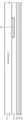
Translated fromKorean도 1은 본 발명에 따른 유기발광 디스플레이의 단위 화소부 구동소자의 개략적 단면도를 보여준다.1 is a schematic cross-sectional view of a driving unit of a pixel unit of an organic light emitting display according to the present invention.
도 2는 도 1에서 제1 듀얼채널층(A영역)의 단면 SEM 사진이다.FIG. 2 is a cross-sectional SEM photograph of the first dual channel layer (region A) in FIG. 1.
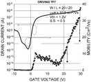
도 3a 및 도 3b 각각은 본 발명에 따른 유기발광 디스플레이의 단위 화소부 구동소자에서 스위칭용 트랜지스터 및 구동용 트랜지스터의 스위칭 특성을 보여주는 그래프이다.3A and 3B are graphs illustrating switching characteristics of the switching transistor and the driving transistor in the unit pixel unit driving device of the organic light emitting display according to the present invention.
도 4a 내지 도 4k는 본 발명에 따른 유기발광 디스플레이의 단위 화소부 구동소자의 제조방법을 보여주는 공정도이다.4A to 4K are flowcharts illustrating a method of manufacturing a unit pixel unit driving device of an organic light emitting display according to the present invention.
도 5는 본 발명에 따른 유기발광 디스플레이의 단위 화소부를 보여주는 개략적 단면도이다.5 is a schematic cross-sectional view illustrating a unit pixel unit of an organic light emitting display according to the present invention.
도 6은 본 발명에 따른 유기발광 디스플레이의 단위 화소부의 주요 구성의 레이아웃을 보여준다.6 shows a layout of main components of a unit pixel portion of an organic light emitting display according to the present invention.
도 7은 본 발명에 따른 유기발광 디스플레이의 개략적 구조를 보여주는 등가회로도이다.7 is an equivalent circuit diagram showing a schematic structure of an organic light emitting display according to the present invention.
< 도면의 주요부분에 대한 부호의 설명 ><Description of Symbols for Major Parts of Drawings>
10:기판 20:제1 게이트 전극10: substrate 20: first gate electrode
22:제1 절연막 24:비정질 실리콘층22: first insulating film 24: amorphous silicon layer
24a:제1 비정질 실리콘층 24b:제2 비정질 실리콘층24a: first
26:다결정 실리콘층 26a:제1 다결정 실리콘층26:
26b:제2 다결정 실리콘층 27a:제1 듀얼채널층26b: second
27b:제2 듀얼채널층 28, 28a, 28b:n-도핑된 실리콘층27b: second
29:전극층 30s:제1 소오스 전극29:
30d:제1 드레인 전극 31s:제2 소오스 전극30d:
31d:제2 드레인 전극 40S:제1 소오스 영역31d:
40D:제1 드레인 영역 41S:제2 소오스 영역40D: first drain
41D:제2 드레인 영역 42:제2 절연막41D: second drain region 42: second insulating film
60:제2 게이트 전극 62:제3 절연막60: second gate electrode 62: third insulating film
70:제1 배선 72:제4 절연막70: first wiring 72: fourth insulating film
80:제2 배선 90:제1 전극80: second wiring 90: first electrode
92:제5 절연막 96:유기발광층92: fifth insulating film 96: organic light emitting layer
98:제2 전극 100:유기발광 소자98: second electrode 100: organic light emitting device
101:스위칭용 트랜지스터 102:구동용 트랜지스터101: switching transistor 102: driving transistor
본 발명은 유기발광 디스플레이의 단위 화소부 구동소자에 관한 것으로, 보다 상세하게는 적은 공정수와 간단하고 쉬운 공정으로 제조될 수 있도록 그 구조가 개선된 유기발광 디스플레이의 단위 화소부 구동소자에 관한 것이다.The present invention relates to a unit pixel unit driving device of an organic light emitting display, and more particularly, to a unit pixel unit driving device of an organic light emitting display whose structure is improved to be manufactured in a low number of steps and a simple and easy process. .
평판 디스플레이(FPD: Flat Panel Display) 분야에서, 지금까지는 가볍고 전력소모가 적은 액정표시장치(LCD)가 가장 주목받는 디스플레이였지만, 상기 액정표시장치가 수광형 디스플레이이기 때문에, 밝기, 콘트라스트(contrast), 시야각 및 대면적화 등에 기술적 한계가 있으며, 이러한 단점을 극복할 수 있는 새로운 평판디스플레이소자에 대한 개발이 활발하게 전개되고 있다.In the field of flat panel displays (FPDs), a light and low power consumption liquid crystal display (LCD) has been the most popular display until now, but since the liquid crystal display is a light-receiving display, brightness, contrast, There are technical limitations such as viewing angle and large area, and development of a new flat panel display device capable of overcoming these disadvantages is being actively developed.
새로운 평판디스플레이 중 하나인 유기 발광 디스플레이는 단위 유기발광 소자(Organic Light Emitting Device:OLED)의 2차원 배열을 가지는 것으로, 자체발광형이기 때문에, 액정표시장치에 비해 시야각, 콘트라스트 등의 특성이 우수하며, 백라이트가 필요하지 않기 때문에, 보다 경량 박형화가 가능하고, 소비전력 측면에서도 유리하다. 또한, 직접 저전압 구동이 가능하고 응답 속도가 빠르며, 전부 고체이기 때문에, 외부 충격에 강하고 사용온도범위도 넓으며 특히, 제조 비용 측면에서도 저렴한 장점을 가지고 있다. 특히, 각 화소마다 스위칭 소자인 트랜지스터를 가지는 액티브 매트릭스 방식으로 유기 발광 디스플레이를 구동하게 되면, 낮은 전류를 인가하더라도 동일한 휘도를 나타내므로, 저소비전력, 고정세 및 대형화가 가능한 장점을 가진다.One of the new flat panel displays, the organic light emitting display has a two-dimensional array of organic light emitting devices (OLEDs). Since the organic light emitting display is a self-luminous type, it has better characteristics such as viewing angle and contrast than liquid crystal displays. Since a backlight is not required, a lighter weight can be made thinner and it is advantageous in terms of power consumption. In addition, since it is possible to directly drive low voltage, fast response speed, and all solid, it is resistant to external shock, wide use temperature range, and in particular, inexpensive in terms of manufacturing cost. In particular, when the organic light emitting display is driven in an active matrix method having a transistor as a switching element for each pixel, the same luminance is displayed even when a low current is applied, and thus, low power consumption, high definition, and large size can be obtained.
상기 액티브 매트릭스 방식 유기 발광 디스플레이의 각 단위 화소부에는, OLED를 구동하기 위해 2개의 박막 트랜지스터(TFT;Thin Film Transistor), 즉 스위칭용 트랜지스터(switching TFT)와 구동용 트랜지스터(driving TFT)가 구비되어야 한다. 상기 스위칭용 트랜지스터는 각 단위 화소부에 공급되는 전류를 온/오프(on/off)하는 역할을 담당하며, 상기 구동용 트랜지스터는 상기 OLED에 할당된 전류를 제공하는 역할을 담당한다. 이러한 역할분담에 따라, 상기 스위칭용 트랜지스터와 구동용 트랜지스터에 요구되는 특성 및 스펙(specification)이 다르다. 예를 들어, 스위칭용 트랜지스터는 누설전류(leakage current)가 작아야 하며, 온/오프 비(on/off ratio)가 커야한다. 반면에, 상기 구동용 트랜지스터는 고이동성(high mobility)과 신뢰성(reliability)을 가질 것이 요구된다. 이와 같은 요구 목적을 만족시키기 위해서, 상기 스위칭용 트랜지스터는 비정질 실리콘 트랜지스터로 형성할 필요가 있고, 구동용 트랜지스터는 다결정 실리콘 트랜지스터로 형성할 필요가 있다. 그러나, 이를 위해 상기 스위칭용 트랜지스터의 제조공정 및 구동용 트랜지스터의 제조공정 각각을 별개로 진행시켜야 하기 때문에, 제조비용과 공정이 복잡해 질 수 있다는 문제점이 있다. 한편, 비정질 실리콘 트랜지스터를 동시에 스위칭용 트랜지스터와 구동용 트랜지스터로 사용할 경우, 상기 비정질 실리콘 트랜지스터가 스위칭용 트랜지스터로서의 가치는 있지만, 전자이동성(electron mobility)나 신뢰성(reliability) 측면에서 기능적으로 떨어지기 때문에, 우수한 특성의 OLED를 구현하기 어렵다는 문제점이 있다. 반대로, 다결정 실리콘 트랜지스터을 스위칭용 트랜지스터로 사용할 경우, 구동용 트랜지스터로서의 가치는 있지만 오프-상태(off-state)에서의 누설전류가 크기 때문에 스위칭용 트랜지스터로서의 기능이 떨어지기 때문에, 우수한 특성의 OLED를 구현하기 어렵다는 문제점이 있다.In each unit pixel portion of the active matrix organic light emitting display, two thin film transistors (TFTs), that is, a switching TFT and a driving TFT, must be provided to drive an OLED. do. The switching transistor plays a role of turning on / off a current supplied to each unit pixel portion, and the driving transistor plays a role of providing a current allocated to the OLED. According to this role-sharing, characteristics and specifications required for the switching transistor and the driving transistor are different. For example, the switching transistor should have a low leakage current and a large on / off ratio. On the other hand, the driving transistor is required to have high mobility and reliability. In order to satisfy such a demanded purpose, the switching transistor needs to be formed of an amorphous silicon transistor, and the driving transistor needs to be formed of a polycrystalline silicon transistor. However, since the manufacturing process of the switching transistor and the manufacturing process of the driving transistor must be performed separately for this purpose, there is a problem that the manufacturing cost and the process can be complicated. On the other hand, when an amorphous silicon transistor is used as a switching transistor and a driving transistor at the same time, the amorphous silicon transistor is valuable as a switching transistor, but is functionally inferior in terms of electron mobility or reliability. There is a problem that it is difficult to implement OLED of excellent characteristics. On the contrary, when the polycrystalline silicon transistor is used as a switching transistor, it is valuable as a driving transistor, but since the leakage current in the off-state is large, the function as the switching transistor is poor, thereby realizing an excellent OLED. There is a problem that is difficult to do.
본 발명이 이루고자 하는 기술적 과제는 상술한 종래기술의 문제점을 개선하기 위한 것으로, 적은 공정수와 간단하고 쉬운 공정으로 제조될 수 있도록 그 구조가 개선된 유기발광 디스플레이의 단위 화소부 구동소자 및 그 제조방법을 제공함에 있다.The technical problem to be achieved by the present invention is to improve the above-mentioned problems of the prior art, the unit pixel unit driving device of the organic light emitting display improved in its structure to be manufactured in a small number of processes and a simple and easy process and its manufacture In providing a method.
본 발명에 따른 유기발광 디스플레이의 단위 화소부 구동소자는,The unit pixel unit driving device of the organic light emitting display according to the present invention,
기판 상에 형성된 상호 연결된 한 조의 스위칭용 트랜지스터와 구동용 트랜지스터를 포함하고,A set of interconnecting switching transistors and driving transistors formed on a substrate,
상기 스위칭용 트랜지스터는 순차적층된 제1 비정질 실리콘층과 제1 다결정 실리콘층을 포함하는 제1 듀얼채널층; 및 상기 제1 듀얼채널층의 하부에 형성되어 상기 제1 비정질 실리콘층과 마주하는 제1 게이트 전극;을 구비하는 하부 게이트 구조로 형성되고,The switching transistor may include a first dual channel layer including a sequential first amorphous silicon layer and a first polycrystalline silicon layer; And a first gate electrode formed under the first dual channel layer to face the first amorphous silicon layer.
상기 구동용 트랜지스터는 순차적층된 제2 비정질 실리콘층과 제2 다결정 실리콘층을 포함하는 제2 듀얼채널층; 및 상기 제2 듀얼채널층의 상부에 형성되어 상기 제2 다결정 실리콘층과 마주하는 제2 게이트 전극;을 구비하는 상부 게이트 구조로 형성된다.The driving transistor may include a second dual channel layer including a second layer of amorphous silicon and a second layer of polycrystalline silicon; And a second gate electrode formed on the second dual channel layer to face the second polycrystalline silicon layer.
본 발명에 따른 유기발광 디스플레이의 단위 화소부 구동소자의 제조방법은,Method of manufacturing a unit pixel unit driving device of an organic light emitting display according to the present invention,
기판 상에 상호 연결된 한 조의 스위칭용 트랜지스터와 구동용 트랜지스터를 형성하되, 상기 스위칭용 트랜지스터는 순차적층된 제1 비정질 실리콘층과 제1 다결정 실리콘층을 포함하는 제1 듀얼채널층; 및 상기 제1 듀얼채널층의 하부에 형성되어 상기 제1 비정질 실리콘층과 마주하는 제1 게이트 전극;을 구비하는 하부 게이트 구조로 형성되고, 상기 구동용 트랜지스터는 순차적층된 제2 비정질 실리콘층과 제2 다결정 실리콘층을 포함하는 제2 듀얼채널층; 및 상기 제2 듀얼채널층의 상부에 형성되어 상기 제2 다결정 실리콘층과 마주하는 제2 게이트 전극;을 구비하는 상부 게이트 구조로 형성되며, 상기 제1 듀얼채널층과 제2 듀얼채널층은 같은 공정에서 동시에 형성되는 것을 특징으로 한다.A pair of switching transistors and a driving transistor formed on the substrate, wherein the switching transistor comprises: a first dual channel layer including a first layer of amorphous silicon and a first polycrystalline silicon layer; And a first gate electrode formed under the first dual channel layer to face the first amorphous silicon layer, wherein the driving transistor comprises a second amorphous silicon layer sequentially formed thereon; A second dual channel layer comprising a second polycrystalline silicon layer; And a second gate electrode formed on the second dual channel layer to face the second polycrystalline silicon layer, wherein the first dual channel layer and the second dual channel layer are the same. It is characterized in that it is formed at the same time in the process.
바람직하게, 상기 스위칭용 트랜지스터를 형성하는 단계는,Preferably, forming the switching transistor,
기판 상에 제1 게이트 전극을 형성하는 단계;Forming a first gate electrode on the substrate;
상기 기판 상에 상기 제1 게이트 전극을 덮는 제1 절연막을 형성하는 단계;Forming a first insulating film covering the first gate electrode on the substrate;
상기 제1 절연막 상에 순차적층된 제1 비정질 실리콘층과 제1 다결정 실리콘층을 포함하는 제1 듀얼채널층을 형성하는 단계; 및Forming a first dual channel layer including a first amorphous silicon layer and a first polycrystalline silicon layer sequentially stacked on the first insulating layer; And
상기 제1 듀얼채널층의 일단부 및 타단부에 각각 제1 소오스 영역 및 제1 드레인 영역을 형성하는 단계;를 포함한다.And forming a first source region and a first drain region at one end and the other end of the first dual channel layer, respectively.
그리고, 상기 구동용 트랜지스터를 형성하는 단계는,In the forming of the driving transistor,
상기 제1 절연막 상에 상기 제1 듀얼채널층과 이격되어 형성되는 것으로, 순차적층된 제2 비정질 실리콘층과 제2 다결정 실리콘층을 포함하는 제2 듀얼채널층을 형성하는 단계;Forming a second dual channel layer on the first insulating layer, the second dual channel layer being spaced apart from the first dual channel layer, the second dual channel layer including a second layer of amorphous silicon and a second polycrystalline silicon layer;
상기 제2 듀얼채널층의 일단부 및 타단부에 각각 제2 소오스 영역 및 제2 드 레인 영역을 형성하는 단계;Forming a second source region and a second drain region at one end and the other end of the second dual channel layer, respectively;
상기 제2 듀얼채널층, 제2 소오스 영역 및 제2 드레인 영역을 덮는 제2 절연막을 형성하는 단계; 및Forming a second insulating layer covering the second dual channel layer, the second source region, and the second drain region; And
상기 제2 절연막 상에 상기 제2 다결정 실리콘층과 마주하도록 제2 게이트 전극을 형성하는 단계;를 포함한다.And forming a second gate electrode on the second insulating layer to face the second polycrystalline silicon layer.
또한, 본 발명에 따른 유기발광 디스플레이는,In addition, the organic light emitting display according to the present invention,
기판 상에 매트릭스 형상으로 형성되는 것으로, 상호 연결된 한 조의 스위칭용 트랜지스터와 구동용 트랜지스터를 포함하는 단위 화소부 구동소자; 및 단위 화소부 유기발광 소자;를 포함하는 복수의 단위 화소부를 구비하고,A unit pixel unit driving element formed on a substrate in a matrix shape and including a pair of switching transistors and a driving transistor connected to each other; And a plurality of unit pixel units including a unit pixel unit organic light emitting diode,
상기 스위칭용 트랜지스터는 순차적층된 제1 비정질 실리콘층과 제1 다결정 실리콘층을 포함하는 제1 듀얼채널층; 및 상기 제1 듀얼채널층의 하부에 형성되어 상기 제1 비정질 실리콘층과 마주하는 제1 게이트 전극;을 구비하는 하부 게이트 구조로 형성되고,The switching transistor may include a first dual channel layer including a sequential first amorphous silicon layer and a first polycrystalline silicon layer; And a first gate electrode formed under the first dual channel layer to face the first amorphous silicon layer.
상기 구동용 트랜지스터는 순차적층된 제2 비정질 실리콘층과 제2 다결정 실리콘층을 포함하는 제2 듀얼채널층; 및 상기 제2 듀얼채널층의 상부에 형성되어 상기 제2 다결정 실리콘층과 마주하는 제2 게이트 전극;을 구비하는 상부 게이트 구조로 형성된다.The driving transistor may include a second dual channel layer including a second layer of amorphous silicon and a second layer of polycrystalline silicon; And a second gate electrode formed on the second dual channel layer to face the second polycrystalline silicon layer.
본 발명에 따르면, 종래 스위칭용 트랜지스터와 구동용 트랜지스터 각각의 채널형성 공정이 별개로 진행되었던 것을, 하나의 공정에서 동시에 형성될 수 있도록 상기 단위 화소부 구동소자의 구조 및 그 제조공정이 개선되었으며, 그 결과 기 존보다 적은 공정수와 간단하고 쉬운 공정으로 유기발광 디스플레이의 단위 화소부 구동소자가 제조될 수 있다.According to the present invention, the structure of the unit pixel unit driving device and its manufacturing process are improved so that the channel forming process of each of the switching transistor and the driving transistor is performed separately in one step. As a result, the unit pixel unit driving device of the organic light emitting display can be manufactured with fewer processes and simpler and easier processes.
이하에서, 본 발명에 따른 유기발광 디스플레이의 단위 화소부 구동소자 및 그 제조방법을 첨부된 도면을 참조하여 상세히 설명한다. 이 과정에서 도면에 도시된 층이나 영역들의 두께는 명세서의 명확성을 위하여 과장되게 도시된 것이다.Hereinafter, the driving unit and the manufacturing method of the unit pixel unit of the organic light emitting display according to the present invention will be described in detail with reference to the accompanying drawings. In the process, the thicknesses of layers or regions illustrated in the drawings are exaggerated for clarity.
도 1은 본 발명에 따른 유기발광 디스플레이의 단위 화소부 구동소자의 개략적 단면도이며, 도 2는 도 1에서 제1 듀얼채널층(A영역)의 단면 SEM 사진이다. 그리고, 도 3a 및 도 3b 각각은 본 발명에 따른 유기발광 디스플레이의 단위 화소부 구동소자에서 스위칭용 트랜지스터(101) 및 구동용 트랜지스터(102)의 스위칭 특성을 보여주는 그래프이다.1 is a schematic cross-sectional view of a driving unit of a unit pixel unit of an organic light emitting display according to the present invention, and FIG. 2 is a cross-sectional SEM photograph of the first dual channel layer (region A) of FIG. 1. 3A and 3B are graphs illustrating switching characteristics of the switching
도 1 및 도 2를 함께 참조하면, 본 발명의 일실시예로 기판(10) 상에 상호 연결된 한 조의 스위칭용 트랜지스터(101, Switching transistor;Tsw)와 구동용 트랜지스터(102, Driving transistor;Tdr)를 포함하는 유기발광 디스플레이의 단위 화소부 구동소자가 형성되었다.1 and 2 together, as an embodiment of the present invention, a set of switching transistors Tsw and a driving
상기 스위칭용 트랜지스터(101)는 순차적층된 제1 비정질 실리콘층(24a)과 제1 다결정 실리콘층(26a)을 포함하는 제1 듀얼채널층(27a) 및 상기 제1 듀얼채널층(27a)의 하부에 형성되어 상기 제1 비정질 실리콘층(24a)과 마주하는 제1 게이트 전극(20)을 구비하여, 도시된 바와 같이 하부 게이트(bottom gate) 구조로 형성된다. 그리고, 상기 제1 듀얼채널층(27a)과 제1 게이트 전극(20) 사이에 제1 절연 막(22)이 개재되었으며, 상기 제1 듀얼채널층(27a)의 일단부 및 타단부에 각각 제1 소오스 영역(40S) 및 제1 드레인 영역(40D)이 형성되었다. 바람직하게, 상기 제1 소오스 영역(40S)은 상기 제1 듀얼채널층(27a)의 일단부 상에 순차로 적층된 n-도핑된 실리콘층(28a, n-doped Si layer) 및 제1 소오스 전극(30s)을 포함할 수 있다. 그리고, 상기 제1 드레인 영역(40D)은 상기 제1 듀얼채널층(27a)의 타단부 상에 순차로 적층된 n-도핑된 실리콘층(28a) 및 제1 드레인 전극(30d)을 포함할 수 있다. 여기에서, 상기 n-도핑된 실리콘층(28a)은 As, P와 같은 n형 도펀트를 포함하는 실리콘층이며, 상기 제1 듀얼채널층(27a)과는 별도의 증착공정으로 형성될 수 있다.The switching
상기 구동용 트랜지스터(102)는 순차적층된 제2 비정질 실리콘층(24b)과 제2 다결정 실리콘층(26b)을 포함하는 제2 듀얼채널층(27b) 및 상기 제2 듀얼채널층(27b)의 상부에 형성되어 상기 제2 다결정 실리콘층(26b)과 마주하는 제2 게이트 전극(60)을 구비하여, 도시된 바와 같이 상부 게이트(Top gate) 구조로 형성된다. 그리고, 상기 제2 듀얼채널층(27b)과 제2 게이트 전극(60) 사이에 제2 절연막(42)이 개재되었으며, 상기 제2 듀얼채널층(27b)의 일단부 및 타단부에 각각 제2 소오스 영역(41S) 및 제2 드레인 영역(41D)이 형성되었다. 바람직하게, 상기 제2 소오스 영역(41S)은 상기 제2 듀얼채널층(27b)의 일단부 상에 순차로 적층된 n-도핑된 실리콘층(28b, n-doped Si layer) 및 제2 소오스 전극(31s)을 포함할 수 있다. 그리고, 상기 제2 드레인 영역(41D)은 상기 제2 듀얼채널층(27b)의 타단부 상에 순차로 적층된 n-도핑된 실리콘층(28b) 및 제2 드레인 전극(31d)을 포함할 수 있다. 여 기에서, 상기 n-도핑된 실리콘층(28b)은 As, P와 같은 n형 도펀트를 포함하는 실리콘층이며, 상기 제2 듀얼채널층(27b)과는 별도의 증착공정으로 형성될 수 있다.The driving
상기 제1 소오스 영역(40S) 또는 제1 드레인 영역(40D)이 상기 제2 게이트 전극(60)과 제1 배선(70, interconnection line)에 의해 상호 연결되어 상기 스위칭용 트랜지스터(101)로부터 구동용 트랜지스터(102)로 전기적 신호가 입력될 수 있다.The
본 발명에 따른 유기발광 디스플레이의 단위 화소부 구동소자의 구조에서, 상기 스위칭용 트랜지스터(101)는 단위 화소부에 공급되는 전류를 온/오프(on/off)하는 역할을 담당하며, 상기 구동용 트랜지스터(102)는 상기 단위 화소부에 형성된 유기발광 소자(미도시, Organic Light Emitting Device:OLED)에 할당되는 전류를 제공하는 역할을 담당할 수 있다. 이러한 역할분담에 따라, 상기 스위칭용 트랜지스터(101)와 구동용 트랜지스터(102)에 요구되는 특성 및 스펙(specification)이 다르다. 예를 들어, 스위칭용 트랜지스터(101)는 누설전류(leakage current)가 작아야 하며, 온/오프 비(on/off ratio)가 커야한다. 반면에, 상기 구동용 트랜지스터(102)는 고이동성(high mobility)과 신뢰성(reliability)을 가질 것이 요구된다. 이와 같은 요구목적에 부합되기 위해서는, 상기 스위칭용 트랜지스터(101)는 비정질 실리콘 트랜지스터로 형성될 필요가 있고, 구동용 트랜지스터(102)는 다결정 실리콘 트랜지스터로 형성될 필요가 있다.In the structure of the unit pixel unit driving element of the organic light emitting display according to the present invention, the switching
이와 같은 필요성으로, 본 발명에 따른 단위 화소부 구동소자는 스위칭용 트랜지스터(101) 및 구동용 트랜지스터(102) 각각에서, 비정질 실리콘층과 다결정 실 리콘층이 순차로 적층된 이중층 구조의 듀얼채널층을 채용하고 있다. 이와 같은 이중층 구조의 듀얼채널층은 게이트 전극과의 배치관계에 따라, 비정질 실리콘 채널 또는 다결정 실리콘 채널 양자의 기능을 모두 수행할 수 있다. 구체적으로, 상기 스위칭용 트랜지스터(101)는, 상기 제1 듀얼채널층(27a)의 하부에 제1 게이트 전극(20)이 배치되는 하부 게이트 구조로 형성되며, 따라서, 상기 제1 비정질 실리콘층(24a)과 제1 게이트 전극(20)이 인접하여 상호 마주하게 된다. 이와 같은 하부 게이트 구조로부터, 상기 제1 듀얼채널층(27a)을 구성하는 제1 비정질 실리콘층(24a)과 제1 다결정 실리콘층(26a) 중 제1 비정질 실리콘층(24a)만을 선택적으로 채널로 이용할 수 있으며, 그 결과, 상기 스위칭용 트랜지스터(101)는 우수한 스위칭 특성을 가지는 비정질 실리콘 트랜지스터로 기능할 수 있다.As a necessity, the unit pixel unit driving device according to the present invention includes a dual channel layer having a double layer structure in which an amorphous silicon layer and a polysilicon layer are sequentially stacked in each of the switching
또한, 상기 구동용 트랜지스터(102)는, 상기 제2 듀얼채널층(27b)의 상부에 제2 게이트 전극(60)이 배치되는 상부 게이트 구조로 형성되며, 따라서, 상기 제2 다결정 실리콘층(26b)과 제2 게이트 전극(60)이 인접하여 상호 마주하게 된다. 이와 같은 상부 게이트 구조로부터, 상기 제2 듀얼채널층(27b)을 구성하는 제2 비정질 실리콘층(24b)과 제2 다결정 실리콘층(26b) 중 제2 다결정 실리콘층(26b)만을 선택적으로 채널로 이용할 수 있으며, 그 결과, 상기 구동용 트랜지스터(102)는 고이동성(high mobility)을 가지는 다결정 실리콘 트랜지스터로 기능할 수 있다.In addition, the driving
바람직하게, 상기 제1 및 제2 비정질 실리콘층(24a, 24b) 각각은 10Å 내지 500Å의 두께로 형성되며, 상기 제1 및 제2 다결정 실리콘층(26a, 26b) 각각은 500Å 내지 3000Å의 두께로 형성될 수 있다.Preferably, each of the first and second
본 발명에 따르면, 종래 스위칭용 트랜지스터와 구동용 트랜지스터 각각의 채널형성 공정이 별개로 진행되었던 것을, 하나의 공정에서 동시에 형성될 수 있도록 상기 단위 화소부 구동소자의 구조가 개선되었으며, 그 결과 기존보다 적은 공정수와 간단하고 쉬운 공정으로 유기발광 디스플레이의 단위 화소부 구동소자가 제조될 수 있다.According to the present invention, the structure of the driving unit of the unit pixel part is improved so that the channel forming process of each of the switching transistor and the driving transistor is performed separately in one process. The unit pixel unit driving element of the organic light emitting display can be manufactured with a small number of processes and a simple and easy process.
도 4a 내지 도 4k는 본 발명에 따른 유기발광 디스플레이의 단위 화소부 구동소자의 제조방법을 보여주는 공정도이다. 상기 도 4a 내지 도 4k에 예시되는 제조공정에서, 각각의 박막은 반도체 제조공정에서 일반적으로 이용되는 박막 증착공정, 예를 들어 PVD(physical vapor deposition), CVD(chemical vapor deposition) 또는 PECVD(plasma enhanced chemical vapor deposition)와 같은 공정에 의해 형성될 수 있다.4A to 4K are flowcharts illustrating a method of manufacturing a unit pixel unit driving device of an organic light emitting display according to the present invention. In the manufacturing process illustrated in FIGS. 4A-4K, each thin film is a thin film deposition process commonly used in a semiconductor manufacturing process, for example, physical vapor deposition (PVD), chemical vapor deposition (CVD), or plasma enhanced PECVD (PECVD). It may be formed by a process such as chemical vapor deposition.
도 4a 내지 도 4d를 참조하면, 먼저 기판(10) 상에 Al 또는 Mo와 같은 게이트 금속을 2000Å 내지 4000Å 두께로 증착시킨 후, 이를 패터닝하여 제1 게이트 전극(20)을 형성한다. 상기 기판(10)은 비정질 기판 또는 절연기판인 것이 바람직하다. 그리고나서, 상기 제1 게이트 전극(20)이 매립되도록 상기 기판(10)의 전면에 SiOx 또는 SiNx와 같은 물질로 제1 절연막(22)을 형성한다. 그 다음에, 상기 제1 절연막(22) 상에 비정질 실리콘층(24)과 다결정 실리콘층(26)을 순차로 형성한다. 상기 비정질 실리콘층(24)은 10Å 내지 500Å의 두께로 형성될 수 있으며, 상기 다결정 실리콘층(26)은 500Å 내지 3000Å의 두께로 형성될 수 있다. 바람직하게, 상 기 비정질 실리콘층(24)과 다결정 실리콘층(26)은 하나의 증착공정에서 연속적으로 형성될 수 있다. 예를 들어, 상기 제1 절연막(22)이 형성된 기판(10)을 PECVD 챔버내에 장입한 후, 상기 챔버 내부의 온도를 20℃ 내지 500℃로 유지하고, 상기 챔버내에 SiH4(gas)와 H2(gas)를 공급하여 이들을 5분 내지 60분 동안 반응시킴으로써, 상기 제1 절연막(22) 상에 상기 비정질 실리콘층(24)과 다결정 실리콘층(26)을 연속적으로 형성시킬 수 있다. 바람직하게, 상기 SiH4(gas)와 H2(gas)의 혼합비에서, 상기 H2(gas)은 90% 내지 99%의 양으로 제어되는 것이 바람직하다. 이 때, 상기 챔버내의 압력은 30 미리토르 내지 10000 미리토르로 제어될 수 있으며, RF 파워는 100W 내지 1000W로 제어될 수 있다.4A to 4D, first, a gate metal such as Al or Mo is deposited to a thickness of 2000 μs to 4000 μm on a
그 다음에, 상기 다결정 실리콘층(26) 상에 n-도핑된 실리콘층(28, n-doped Si layer)을 200Å 내지 1000Å 두께로 형성한다. 여기에서, n 도펀트로 As 또는 P을 이용하며, 상기 n 도펀트는 SiH4(gas) 및 H2(gas)와 함께 상기 챔버내에 공급된다. 본 공정에서는 상기 n-도핑된 실리콘층(28)이 별도의 증착공정으로 형성되었지만, 이에만 한정되는 것은 아니며, 이온주입법과 같은 다른 방법에 의해서도 형성될 수 있을 것이다.Subsequently, an n-doped
그 다음에, 상기 n-도핑된 실리콘층(28), 다결정 실리콘층(26) 및 비정질 실리콘층(24)을 패터닝하여 상호 이격된 제1, 제2 채널부를 형성한다. 여기에서, 상기 제1 채널부는 순차적층된 제1 비정질 실리콘층(24a)과 제1 다결정 실리콘층(26a)을 포함하는 제1 듀얼채널층(27a)과 상기 제1 듀얼채널층(27a) 상에 적층된 n-도핑된 실리콘층(28a)을 포함한다. 그리고, 상기 제2 채널부는 순차적층된 제2 비정질 실리콘층(24b)과 제2 다결정 실리콘층(26b)을 포함하는 제2 듀얼채널층(27b)과 상기 제2 듀얼채널층(27b) 상에 적층된 n-도핑된 실리콘층(28b)을 포함한다.The n-doped
도 4e 내지 도 4g를 참조하면, 상기 제1 절연막(22) 상에 Al 또는 Mo와 같은 금속으로 상기 제1, 제2 채널부를 덮는 전극층(29)을 2000Å 내지 4000Å 두께로 형성한 후, 이를 패터닝하여 상기 제1 채널부의 일단부 및 타단부 각각에 제1 소오스 전극(30s)과 제1 드레인 전극(30d)을 형성하고, 상기 제2 채널부의 일단부 및 타단부 각각에 제2 소오스 전극(31s) 및 제2 드레인 전극(31d)을 형성한다.Referring to FIGS. 4E to 4G, after forming the
그 다음에, 상기 제1 소오스 전극(30s)과 제1 드레인 전극(30d)을 연결하는 상기 n-도핑된 실리콘층(28a)의 영역을 선택적으로 식각하여, 상기 제1 다결정 실리콘층(26a)의 상면을 노출시킨다. 이 때, 상기 제1 소오스 전극(30s)과 제1 드레인 전극(30d)을 마스크로 이용하여, 상기 n-도핑된 실리콘층(28a)의 식각공정을 수행할 수 있다. 바람직하게, 상기 제1 소오스 전극(30s)과 제1 드레인 전극(30d)을 형성하기 위한 상기 전극층(29)의 패터닝 공정과 상기 n-도핑된 실리콘층(28a)의 식각공정이 한번에 같이 수행될 수 있다.Then, the region of the n-doped
또한, 상기 n-도핑된 실리콘층(28a)의 식각공정과 같은 방법으로, 상기 제2 소오스 전극(31s)과 제2 드레인 전극(31d)을 연결하는 상기 n-도핑된 실리콘층(28b)의 영역을 선택적으로 식각하여, 상기 제2 다결정 실리콘층(26b)의 상면을 노출시킨다. 이 때, 상기 제2 소오스 전극(31s)과 제2 드레인 전극(31d)을 마스크 로 이용하여, 상기 n-도핑된 실리콘층(28b)의 식각공정을 수행할 수 있다. 바람직하게, 상기 제2 소오스 전극(31s)과 제2 드레인 전극(31d)을 형성하기 위한 상기 전극층(29)의 패터닝 공정과 상기 n-도핑된 실리콘층(28b)의 식각공정이 한번에 같이 수행될 수 있다. 도 4g의 공정을 수행한 결과, 상기 제1 듀얼채널층(27a)의 일단부 및 타단부 각각에 제1 소오스 영역(40S) 및 제1 드레인 영역(40D)가 형성될 수 있다. 여기에서, 상기 제1 소오스 영역(40S)은 순차로 적층된 n-도핑된 실리콘층(28a) 및 제1 소오스 전극(30s)을 포함하고, 상기 제1 드레인 영역(40D)은 순차로 적층된 n-도핑된 실리콘층(28a) 및 제1 드레인 전극(30d)을 포함한다. 마찬가지로, 상기 제2 듀얼채널층(27b)의 일단부 및 타단부 각각에 제2 소오스 영역(41S) 및 제2 드레인 영역(41D)가 형성될 수 있다. 여기에서, 상기 제2 소오스 영역(41S)은 순차로 적층된 n-도핑된 실리콘층(28b) 및 제2 소오스 전극(31s)을 포함하고, 상기 제2 드레인 영역(41D)은 순차로 적층된 n-도핑된 실리콘층(28b) 및 제2 드레인 전극(31d)을 포함한다.In addition, in the same manner as the etching process of the n-doped
도 4h를 참조하면, 상기 제1 듀얼채널층(27a), 제2 듀얼채널층(27b), 제1 소오스 영역(40S), 제1 드레인 영역(40D), 제2 소오스 영역(41S) 및 제2 드레인 영역(41D)이 모두 매립되도록, 상기 제1 절연막(22) 상에 SiOx 또는 SiNx와 같은 물질로 제2 절연막(42)을 형성한다. 그 다음에, 상기 제2 절연막(42) 상에 Al 또는 Mo와 같은 게이트 금속을 2000Å 내지 4000Å 두께로 증착시킨 후, 이를 패터닝하여 제2 게이트 전극(60)을 형성한다.Referring to FIG. 4H, the first
도 4i 내지 도 4k를 참조하면, 상기 제1 드레인 전극(30d)으로부터 상기 제2 게이트 전극(60)으로 전기적 신호가 입력될 수 있도록, 제1 배선(70, interconnection line)으로 이들을 상호 연결한다. 구체적으로, 상기 제2 게이트 전극(60)을 매립하도록 상기 제2 절연막(42) 상에 SiOx 또는 SiNx와 같은 물질로 제3 절연막(62)을 형성한다. 그리고 나서, 상기 제3 절연막(62)과 제2 절연막(42)의 일부 영역을 식각하여, 상기 제1 드레인 전극(30d)의 일부 영역을 노출시키는 제1 콘택홀(h1)과, 상기 제2 게이트 전극(60)의 일부 영역을 노출시키는 제2 콘택홀(h2)을 형성한다. 그리고나서, 제1, 제2 콘택홀(h1, h2) 각각에 Al 또는 Mo와 같은 도전성 물질을 채워넣어, 상기 제1 드레인 전극(30d)과 제2 게이트 전극(60)을 연결하는 제1 배선(70)을 형성한다. 이와 같은 공정과정을 통하여, 본 발명에 따른 유기발광 디스플레이의 단위 화소부 구동소자가 제조될 수 있다. 특히, 본 발명에 따르면, 종래 스위칭용 트랜지스터와 구동용 트랜지스터 각각의 채널형성 공정이 별개로 진행되었던 것을, 하나의 공정에서 동시에 형성될 수 있도록 상기 단위 화소부 구동소자의 구조 및 그 제조공정이 개선되었으며, 그 결과 기존보다 적은 공정수와 간단하고 쉬운 공정으로 유기발광 디스플레이의 단위 화소부 구동소자가 제조될 수 있었다.4I to 4K, interconnects are connected to each other by a
도 5는 본 발명에 따른 유기발광 디스플레이의 단위 화소부를 보여주는 개략적 단면도이며, 도 6은 본 발명에 따른 유기발광 디스플레이의 단위 화소부의 주요 구성의 레이아웃을 보여준다. 그리고, 도 7은 본 발명에 따른 유기발광 디스플 레이의 개략적 구조를 보여주는 등가회로도이다. 5 is a schematic cross-sectional view showing a unit pixel portion of an organic light emitting display according to the present invention, and FIG. 6 shows a layout of main components of a unit pixel portion of an organic light emitting display according to the present invention. 7 is an equivalent circuit diagram illustrating a schematic structure of an organic light emitting display according to the present invention.
도 5 내지 도 7을 함께 참조하면, 본 발명에 따른 유기발광 디스플레이는, 기판(10) 상에 매트릭스 형상으로 배치되는 것으로, 상호 연결된 한 조의 스위칭용 트랜지스터(101)와 구동용 트랜지스터(102)를 포함하는 단위 화소부 구동소자 및 단위 화소부 유기발광 소자(100, organic light emitting;OLED)를 포함하는 복수의 단위 화소부(unit pixel;P)를 구비한다. 여기에서, 상기 스위칭용 트랜지스터(101)와 구동용 트랜지스터(102)를 포함하는 단위 화소부 구동소자의 구조 및 그 제조방법에 대하여는, 이미 전술한 바 있으므로, 중복되는 설명은 생략하기로 한다.5 to 7 together, the organic light emitting display according to the present invention is disposed in a matrix shape on the
도 5를 참조하면, 상기 단위 화소부 유기발광 소자(100)는 순차로 적층된 제1 전극(90), 유기발광층(96) 및 제2 전극(98)을 포함한다. 상기 제1 전극은 ITO(indium tin oxide)와 같은 투명전도성 물질로 형성될 수 있으며, 애노드로서 기능한다. 상기 유기발광층(96)의 형성물질 및 제조방법은 본 발명이 속하는 기술분야에서 통상의 지식을 가진 자에게 이미 널리 알려져 있으므로 이에 대한 상세한 설명은 생략하기로 한다. 상기 제2 전극(98)은 Al 또는 Ag와 같은 도전성 물질로 형성될 수 있으며, 캐소드로서 기능한다. 그리고, 상기 유기발광 소자(100)의 제1 전극(90)은 제2 배선(80)에 의해 상기 구동용 트랜지스터(102)의 제2 드레인 전극(31d)와 연결되도록 형성되어 있다.Referring to FIG. 5, the unit pixel unit organic light emitting diode 100 includes a
상기 단위 화소부 유기발광 소자(100)의 제조방법을 살펴보면, 도 4k의 공정에 연속하여 상기 제3 절연막(62)의 전면에 상기 제1 배선(70)을 매립하도록 SiOx 또는 SiNx와 같은 물질로 제4 절연막(72)을 형성한다. 그리고나서, 상기 제2, 제3, 제4 절연막(42, 62, 72)을 순차로 식각하여, 상기 제2 드레인 전극(31d)의 일부 영역을 노출시키는 제3 콘택트홀(h3)을 형성한다. 그리고나서, 상기 제3 콘택트홀(h3)에 ITO와 같은 투명전도성 물질을 채워 제2 배선을 형성한다. 그리고나서, 상기 제2 배선과 접촉되도록, 상기 제4 절연막(72) 상에 ITO와 같은 투명전도성 물질로 상기 제1 전극(90)을 형성한다. 그 다음에, 상기 제1 전극(90)을 매립하도록 상기 제4 절연막(72)의 전면에 SiOx 또는 SiNx와 같은 물질로 제5 절연막(92)을 형성한다. 그리고나서, 상기 제5 절연막(92)의 일부 영역을 식각하여, 상기 제1 전극(90)을 노출시키는 제4 콘택트홀(h4)을 형성한다. 그 다음에, 상기 제1 전극(90)을 덮도록 상기 제5 절연막(92) 상에 유기발광층(96)을 형성하고, 상기 유기발광층(96) 상에 Al 또는 Ag와 같은 도전성 물질로 제2 전극(98)을 형성한다.Looking at the manufacturing method of the organic light emitting device 100 of the unit pixel portion, such as SiOx or SiNx to bury the
도 6 및 도 7을 함께 참조하면, 본 발명에 따른 유기 발광 디스플레이에서, 스위칭용 트랜지스터(101, Tsw)의 제1 소오스 전극(30s)은 예컨대, 수평 구동 회로(Horizontal driving circuit)로부터 데이터 신호가 입력되는 데이터 라인(Data line:DL)에 전기적으로 연결된다. 이를 통하여, 데이터 라인(DL)은 스위칭용 트랜지스터(101, Tsw)의 제1 소오스 전극(30s) 및 제1 드레인 전극(30d)을 통하여 구동용 트랜지스터(102, Tdr)의 제2 게이트 전극(60)에 전기적으로 연결될 수 있다. 상기 스위칭용 트랜지스터(101)의 제1 게이트 전극(20)은 수직 스캐닝 회로(Vertical scanning circuit)로부터 선택 신호가 입력되는 선택 라인(select line:SL)에 전기적으로 연결된다. 그리고, 상기 구동용 트랜지스터(102)의 제2 소오스 전극(31s)은 전력 공급 회로(Power circuit)로부터 구동 전력이 공급되는 전력 공급 라인(Power line:PL)에 전기적으로 연결된다. 이를 통하여, 전력 공급 라인(PL)은 구동용 트랜지스터(102)의 제2 소오스 전극(31s) 및 제2 드레인 전극(31d)을 통하여 각각의 단위 화소부 유기발광 소자(100, OLED)에 연결될 수 있다.6 and 7 together, in the organic light emitting display according to the present invention, the
상기 데이터 라인(DL) 및 선택 라인(SL)은 직교하는 방향으로 교차하도록 배치되며, 교차되는 데이터 라인 및 선택 라인(SL)에 의해 각 단위 화소부(unit pixel;P)가 정의된다. 한편, 서로 연결된 스위칭용 트랜지스터(101)의 제1 드레인 전극(30d) 및 상기 구동용 트랜지스터(102)의 제2 게이트 전극(60)으로부터 연장된 부분과 상기 전력 공급 라인(PL)은 도 7에서의 스토리지 커패시터(Cs)를 이룰 수 있다.The data line DL and the selection line SL are disposed to intersect in a direction perpendicular to each other, and each unit pixel portion P is defined by the data line and the selection line SL that cross each other. Meanwhile, a portion extending from the
본 발명에 따르면, 일련의 연속적인 공정에 의해 한 조의 스위칭용 트랜지스터와 구동용 트랜지스터를 포함하는 유기발광 디스플레이의 단위 화소부 구동소자가 제조될 수 있다. 특히, 본 발명에 따르면, 종래 스위칭용 트랜지스터와 구동용 트랜지스터 각각의 채널형성 공정이 별개로 진행되었던 것을, 하나의 공정에서 동시에 형성될 수 있도록 상기 단위 화소부 구동소자의 구조 및 그 제조공정이 개선되었으며, 그 결과 기존보다 적은 공정수와 간단하고 쉬운 공정으로 유기발광 디스 플레이의 단위 화소부 구동소자가 제조될 수 있었다. 따라서, 제품제조상의 불량률을 감소시켜 제조수율을 높이면서, 제조상의 재현성 및 신뢰성도 향상시킬 수 있다.According to the present invention, a unit pixel unit driving element of an organic light emitting display including a set of switching transistors and a driving transistor can be manufactured by a series of continuous processes. Particularly, according to the present invention, the channel forming process of each of the switching transistor and the driving transistor is performed separately, so that the structure of the unit pixel unit driving element and the manufacturing process thereof are improved so that they can be simultaneously formed in one process. As a result, the unit pixel unit driving device of the organic light emitting display can be manufactured with fewer processes and a simpler and easier process. Therefore, while reducing the defect rate in manufacturing the product to increase the manufacturing yield, it is possible to improve the reproducibility and reliability in manufacturing.
이상에서, 이러한 본원 발명의 이해를 돕기 위하여 몇몇의 모범적인 실시예가 설명되고 첨부된 도면에 도시되었으나, 이러한 실시예들은 예시적인 것에 불과하며 당해 분야에서 통상적 지식을 가진 자라면 상기 실시예로부터 다양한 변형 및 균등한 타 실시예가 가능하다는 점이 이해되어야 할 것이다. 따라서, 본 발명은 도시되고 설명된 구조와 공정순서에만 국한되는 것은 아니며, 특허청구범위에 기재된 발명의 기술사상을 중심으로 보호되어야 할 것이다.In the above, some exemplary embodiments have been described and illustrated in the accompanying drawings in order to facilitate understanding of the present invention, but these embodiments are merely exemplary and various modifications from the embodiments can be made by those skilled in the art. And it should be understood that other equivalent embodiments are possible. Therefore, the present invention is not limited to the illustrated and described structures and process sequences, but should be protected based on the technical spirit of the invention described in the claims.
Claims (36)
Translated fromKoreanPriority Applications (2)
| Application Number | Priority Date | Filing Date | Title |
|---|---|---|---|
| KR1020060116057AKR101281167B1 (en) | 2006-11-22 | 2006-11-22 | Driving device for unit pixel of organic light emitting display and method of manufacturing the same |
| US11/877,308US8405161B2 (en) | 2006-11-22 | 2007-10-23 | Driving device for unit pixel of organic light emitting display and method of manufacturing the same |
Applications Claiming Priority (1)
| Application Number | Priority Date | Filing Date | Title |
|---|---|---|---|
| KR1020060116057AKR101281167B1 (en) | 2006-11-22 | 2006-11-22 | Driving device for unit pixel of organic light emitting display and method of manufacturing the same |
Publications (2)
| Publication Number | Publication Date |
|---|---|
| KR20080046508Atrue KR20080046508A (en) | 2008-05-27 |
| KR101281167B1 KR101281167B1 (en) | 2013-07-02 |
Family
ID=39416041
Family Applications (1)
| Application Number | Title | Priority Date | Filing Date |
|---|---|---|---|
| KR1020060116057AExpired - Fee RelatedKR101281167B1 (en) | 2006-11-22 | 2006-11-22 | Driving device for unit pixel of organic light emitting display and method of manufacturing the same |
Country Status (2)
| Country | Link |
|---|---|
| US (1) | US8405161B2 (en) |
| KR (1) | KR101281167B1 (en) |
Cited By (14)
| Publication number | Priority date | Publication date | Assignee | Title |
|---|---|---|---|---|
| KR101048965B1 (en)* | 2009-01-22 | 2011-07-12 | 삼성모바일디스플레이주식회사 | Organic electroluminescent display |
| US8134152B2 (en) | 2009-01-13 | 2012-03-13 | Samsung Mobile Display Co., Ltd. | CMOS thin film transistor, method of fabricating the same and organic light emitting display device having laminated PMOS poly-silicon thin film transistor with a top gate configuration and a NMOS oxide thin film transistor with an inverted staggered bottom gate configuration |
| US9214508B2 (en) | 2014-02-24 | 2015-12-15 | Lg Display Co., Ltd. | Thin film transistor substrate with intermediate insulating layer and display using the same |
| US9691799B2 (en) | 2014-02-24 | 2017-06-27 | Lg Display Co., Ltd. | Thin film transistor substrate and display using the same |
| US9721498B2 (en) | 2013-11-11 | 2017-08-01 | Samsung Display Co., Ltd. | Organic light emitting diode display |
| US9721973B2 (en) | 2014-02-24 | 2017-08-01 | Lg Display Co., Ltd. | Thin film transistor substrate and display using the same |
| US9881986B2 (en) | 2014-02-24 | 2018-01-30 | Lg Display Co., Ltd. | Thin film transistor substrate and display using the same |
| KR20180137596A (en)* | 2009-11-06 | 2018-12-27 | 가부시키가이샤 한도오따이 에네루기 켄큐쇼 | Semiconductor device and manufacturing method thereof |
| US10186528B2 (en) | 2014-02-24 | 2019-01-22 | Lg Display Co., Ltd. | Thin film transistor substrate and display using the same |
| US10325937B2 (en) | 2014-02-24 | 2019-06-18 | Lg Display Co., Ltd. | Thin film transistor substrate with intermediate insulating layer and display using the same |
| US10903246B2 (en) | 2014-02-24 | 2021-01-26 | Lg Display Co., Ltd. | Thin film transistor substrate and display using the same |
| US10985196B2 (en) | 2014-02-24 | 2021-04-20 | Lg Display Co., Ltd. | Thin film transistor substrate with intermediate insulating layer and display using the same |
| KR20210081710A (en)* | 2019-12-24 | 2021-07-02 | 엘지디스플레이 주식회사 | Display apparatus comprising different types of thin film transistors and mehthod for manufacturing the same |
| KR20210128503A (en)* | 2009-10-16 | 2021-10-26 | 가부시키가이샤 한도오따이 에네루기 켄큐쇼 | Semiconductor device |
Families Citing this family (36)
| Publication number | Priority date | Publication date | Assignee | Title |
|---|---|---|---|---|
| KR100908472B1 (en)* | 2007-11-20 | 2009-07-21 | 주식회사 엔씰텍 | Thin film transistor, method of manufacturing the same, flat panel display including the same, and manufacturing method thereof |
| KR101506671B1 (en)* | 2008-02-20 | 2015-03-27 | 삼성디스플레이 주식회사 | Organic light emitting display and manufacturing method thereof |
| KR101540341B1 (en)* | 2008-10-17 | 2015-07-30 | 삼성전자주식회사 | PANEL STRUCTURE, DISPLAY DEVICE COMPRISING PANEL STRUCTURE AND METHOD FOR MANUFACTURING |
| JP2010135384A (en)* | 2008-12-02 | 2010-06-17 | Mitsubishi Electric Corp | Thin film transistor array substrate, manufacturing method thereof, and liquid crystal display device |
| TW201023341A (en)* | 2008-12-12 | 2010-06-16 | Ind Tech Res Inst | Integrated circuit structure |
| CN101872779B (en)* | 2009-04-21 | 2014-01-22 | 群创光电股份有限公司 | Image display system and manufacturing method thereof |
| KR101073301B1 (en)* | 2009-07-15 | 2011-10-12 | 삼성모바일디스플레이주식회사 | Organic Light emitting Display device and fabrication method thereof |
| US8471255B2 (en)* | 2009-08-27 | 2013-06-25 | Sharp Kabushiki Kaisha | Bottom-gate thin-film transistor having a multilayered channel and method for manufacturing same |
| KR101073542B1 (en)* | 2009-09-03 | 2011-10-17 | 삼성모바일디스플레이주식회사 | Organic light emitting diode display and method for manufacturing the same |
| TWI411105B (en)* | 2009-09-29 | 2013-10-01 | Ind Tech Res Inst | Active matrix substrates, oled display devices and fabrication methods thereof |
| KR102250803B1 (en) | 2009-12-04 | 2021-05-11 | 가부시키가이샤 한도오따이 에네루기 켄큐쇼 | Semiconductor device |
| CN102269900B (en)* | 2010-06-03 | 2013-04-24 | 北京京东方光电科技有限公司 | Thin film transistor (TFT) array substrate and making method thereof |
| CN102315245A (en)* | 2010-07-09 | 2012-01-11 | 卡西欧计算机株式会社 | Transistor configurations body and light-emitting device |
| JP2012019122A (en)* | 2010-07-09 | 2012-01-26 | Casio Comput Co Ltd | Transistor structure, method for manufacturing transistor structure, and light emitting device |
| JP2012019119A (en)* | 2010-07-09 | 2012-01-26 | Casio Comput Co Ltd | Transistor structure, method for manufacturing transistor structure, and light emitting device |
| TW201218367A (en)* | 2010-09-14 | 2012-05-01 | Casio Computer Co Ltd | Transistor structure, manufacturing method of transistor structure, and light emitting apparatus |
| JP5630170B2 (en)* | 2010-09-14 | 2014-11-26 | カシオ計算機株式会社 | Method for manufacturing transistor structure |
| JP5630169B2 (en)* | 2010-09-14 | 2014-11-26 | カシオ計算機株式会社 | Method for manufacturing transistor structure |
| GB2485828B (en)* | 2010-11-26 | 2015-05-13 | Plastic Logic Ltd | Electronic devices |
| TWI743509B (en) | 2011-05-05 | 2021-10-21 | 日商半導體能源研究所股份有限公司 | Semiconductor device and method for manufacturing the same |
| JP6006930B2 (en)* | 2011-11-22 | 2016-10-12 | 株式会社ジャパンディスプレイ | Thin film transistor circuit board and manufacturing method thereof |
| CN103077957B (en)* | 2013-02-22 | 2015-09-02 | 深圳市华星光电技术有限公司 | Active matrix organic LED display device and preparation method thereof |
| CN105161516B (en)* | 2015-08-13 | 2018-10-30 | 深圳市华星光电技术有限公司 | Organic light emitting display and its manufacturing method |
| CN105679763A (en)* | 2016-01-05 | 2016-06-15 | 深圳市华星光电技术有限公司 | Array substrate and manufacturing method thereof and display panel |
| JP2017143135A (en)* | 2016-02-09 | 2017-08-17 | 株式会社ジャパンディスプレイ | Thin film transistor |
| CN105931988B (en)* | 2016-05-30 | 2019-12-24 | 深圳市华星光电技术有限公司 | Manufacturing method of AMOLED pixel driving circuit |
| JP2016213508A (en)* | 2016-09-07 | 2016-12-15 | 株式会社ジャパンディスプレイ | Thin film transistor circuit substrate |
| CN106653861B (en)* | 2017-01-03 | 2019-08-02 | 京东方科技集团股份有限公司 | A kind of thin film transistor (TFT) and preparation method thereof, array substrate and preparation method thereof |
| CN107170748B (en)* | 2017-04-20 | 2019-11-08 | 上海天马微电子有限公司 | Array substrate, display panel and display device |
| KR102446823B1 (en) | 2017-06-16 | 2022-09-26 | 삼성디스플레이 주식회사 | Display device and manufacturing method thereof |
| KR102263122B1 (en) | 2017-10-19 | 2021-06-09 | 삼성디스플레이 주식회사 | Transistor panel |
| CN109545751B (en)* | 2018-10-15 | 2022-02-22 | Tcl华星光电技术有限公司 | Method for manufacturing thin film transistor array substrate |
| KR102039838B1 (en) | 2018-10-19 | 2019-11-27 | 한국광기술원 | Micro led display pixel assembly and method for manufacturing the same |
| KR102655208B1 (en)* | 2018-12-21 | 2024-04-04 | 엘지디스플레이 주식회사 | Thin film trnasistor having multi-layered gate insulating layer, method of manufacturing the same and display device comprising the same |
| KR102701984B1 (en)* | 2018-12-26 | 2024-09-02 | 엘지디스플레이 주식회사 | Display apparatus comprising different types of thin film transistors and mehthod for manufacturing the same |
| WO2022104576A1 (en)* | 2020-11-18 | 2022-05-27 | 京东方科技集团股份有限公司 | Display substrate and manufacturing method therefor, and display apparatus |
Family Cites Families (10)
| Publication number | Priority date | Publication date | Assignee | Title |
|---|---|---|---|---|
| KR950002202B1 (en)* | 1992-07-01 | 1995-03-14 | 현대전자산업주식회사 | Method of manufacturing multilayer thin film transistor |
| TW554638B (en)* | 2000-05-12 | 2003-09-21 | Semiconductor Energy Lab | Light emitting device |
| JP2002033481A (en) | 2000-07-14 | 2002-01-31 | Sony Corp | Thin-film semiconductor device |
| JP2003223120A (en) | 2002-01-30 | 2003-08-08 | Sanyo Electric Co Ltd | Semiconductor display device |
| KR100556347B1 (en) | 2002-12-30 | 2006-03-03 | 엘지.필립스 엘시디 주식회사 | LCD and its manufacturing method |
| KR100711001B1 (en)* | 2003-12-29 | 2007-04-24 | 엘지.필립스 엘시디 주식회사 | Organic electroluminescent device |
| KR101087750B1 (en)* | 2004-11-29 | 2011-11-30 | 엘지디스플레이 주식회사 | Array substrate for liquid crystal display device comprising two types of thin film transistors and manufacturing method thereof |
| KR101051004B1 (en) | 2004-12-01 | 2011-07-26 | 엘지디스플레이 주식회사 | An array substrate for LCD with type TFT and method of fabrication thereof |
| JP2006178031A (en) | 2004-12-21 | 2006-07-06 | Seiko Epson Corp | Electro-optical device, electronic equipment |
| WO2007037926A2 (en)* | 2005-09-23 | 2007-04-05 | Sharp Laboratories Of America, Inc. | Mems pixel sensor |
- 2006
- 2006-11-22KRKR1020060116057Apatent/KR101281167B1/ennot_activeExpired - Fee Related
- 2007
- 2007-10-23USUS11/877,308patent/US8405161B2/ennot_activeExpired - Fee Related
Cited By (26)
| Publication number | Priority date | Publication date | Assignee | Title |
|---|---|---|---|---|
| US8134152B2 (en) | 2009-01-13 | 2012-03-13 | Samsung Mobile Display Co., Ltd. | CMOS thin film transistor, method of fabricating the same and organic light emitting display device having laminated PMOS poly-silicon thin film transistor with a top gate configuration and a NMOS oxide thin film transistor with an inverted staggered bottom gate configuration |
| KR101048965B1 (en)* | 2009-01-22 | 2011-07-12 | 삼성모바일디스플레이주식회사 | Organic electroluminescent display |
| US12243881B2 (en) | 2009-10-16 | 2025-03-04 | Semiconductor Energy Laboratory Co., Ltd. | Logic circuit and semiconductor device |
| US11756966B2 (en) | 2009-10-16 | 2023-09-12 | Semiconductor Energy Laboratory Co., Ltd. | Logic circuit and semiconductor device |
| KR20220150429A (en)* | 2009-10-16 | 2022-11-10 | 가부시키가이샤 한도오따이 에네루기 켄큐쇼 | Semiconductor device |
| KR20210128503A (en)* | 2009-10-16 | 2021-10-26 | 가부시키가이샤 한도오따이 에네루기 켄큐쇼 | Semiconductor device |
| US11107838B2 (en) | 2009-11-06 | 2021-08-31 | Semiconductor Energy Laboratory Co., Ltd. | Transistor comprising an oxide semiconductor |
| KR20210096328A (en)* | 2009-11-06 | 2021-08-04 | 가부시키가이샤 한도오따이 에네루기 켄큐쇼 | Semiconductor device and manufacturing method thereof |
| KR20180137596A (en)* | 2009-11-06 | 2018-12-27 | 가부시키가이샤 한도오따이 에네루기 켄큐쇼 | Semiconductor device and manufacturing method thereof |
| US12080720B2 (en) | 2009-11-06 | 2024-09-03 | Semiconductor Energy Laboratory Co., Ltd. | Semiconductor device and manufacturing method thereof |
| US10249647B2 (en) | 2009-11-06 | 2019-04-02 | Semiconductor Energy Laboratory Co., Ltd. | Semiconductor device and display device comprising oxide semiconductor layer |
| US11776968B2 (en) | 2009-11-06 | 2023-10-03 | Semiconductor Energy Laboratory Co., Ltd. | Semiconductor device comprising oxide semiconductor layer |
| US10868046B2 (en) | 2009-11-06 | 2020-12-15 | Semiconductor Energy Laboratory Co., Ltd. | Semiconductor device applying an oxide semiconductor |
| US20210288079A1 (en) | 2009-11-06 | 2021-09-16 | Semiconductor Energy Laboratory Co., Ltd. | Semiconductor device and manufacturing method thereof |
| US11107840B2 (en) | 2009-11-06 | 2021-08-31 | Semiconductor Energy Laboratory Co., Ltd. | Method for fabricating a semiconductor device comprising an oxide semiconductor |
| US9721498B2 (en) | 2013-11-11 | 2017-08-01 | Samsung Display Co., Ltd. | Organic light emitting diode display |
| US10325937B2 (en) | 2014-02-24 | 2019-06-18 | Lg Display Co., Ltd. | Thin film transistor substrate with intermediate insulating layer and display using the same |
| US9721973B2 (en) | 2014-02-24 | 2017-08-01 | Lg Display Co., Ltd. | Thin film transistor substrate and display using the same |
| US10985196B2 (en) | 2014-02-24 | 2021-04-20 | Lg Display Co., Ltd. | Thin film transistor substrate with intermediate insulating layer and display using the same |
| US10903246B2 (en) | 2014-02-24 | 2021-01-26 | Lg Display Co., Ltd. | Thin film transistor substrate and display using the same |
| US9691799B2 (en) | 2014-02-24 | 2017-06-27 | Lg Display Co., Ltd. | Thin film transistor substrate and display using the same |
| US9455279B2 (en) | 2014-02-24 | 2016-09-27 | Lg Display Co., Ltd. | Thin film transistor substrate and display using the same |
| US9881986B2 (en) | 2014-02-24 | 2018-01-30 | Lg Display Co., Ltd. | Thin film transistor substrate and display using the same |
| US10186528B2 (en) | 2014-02-24 | 2019-01-22 | Lg Display Co., Ltd. | Thin film transistor substrate and display using the same |
| US9214508B2 (en) | 2014-02-24 | 2015-12-15 | Lg Display Co., Ltd. | Thin film transistor substrate with intermediate insulating layer and display using the same |
| KR20210081710A (en)* | 2019-12-24 | 2021-07-02 | 엘지디스플레이 주식회사 | Display apparatus comprising different types of thin film transistors and mehthod for manufacturing the same |
Also Published As
| Publication number | Publication date |
|---|---|
| US20080116457A1 (en) | 2008-05-22 |
| KR101281167B1 (en) | 2013-07-02 |
| US8405161B2 (en) | 2013-03-26 |
Similar Documents
| Publication | Publication Date | Title |
|---|---|---|
| KR101281167B1 (en) | Driving device for unit pixel of organic light emitting display and method of manufacturing the same | |
| US9917117B2 (en) | Display device and method of fabricating the same | |
| US6873100B2 (en) | Organic electro luminescent display device and method of fabricating the same | |
| TW595026B (en) | Organic electroluminescent display device | |
| CN100542361C (en) | Electroluminescence display device and manufacturing method thereof | |
| CN100395892C (en) | Organic electroluminescence device and manufacturing method thereof | |
| CN106783871B (en) | Array substrate, display panel and manufacturing method | |
| KR101138869B1 (en) | Method of manufacturing driving-device for unit pixel of organic light emitting display | |
| CN105355646B (en) | Array substrate and preparation method thereof, display device | |
| TWI248322B (en) | Organic electro luminescence device and fabrication method thereof | |
| US8025544B2 (en) | Method for manufacturing dual panel-type organic electroluminescent display device | |
| KR100579548B1 (en) | Organic EL device and method of manufacturing the same | |
| CN106992185B (en) | Thin film transistor substrate, display including the same, and manufacturing method thereof | |
| TWI555187B (en) | Organic electroluminescence emitting display and method of manufacturing the same | |
| US9048458B2 (en) | Method of fabricating pixel structure for organic light-emitting display | |
| US6927536B2 (en) | Organic electroluminescent display device with insulating layer patterns and method of fabricating the same | |
| US20240032336A1 (en) | Array substrate, manufacturing method thereof, and organic light-emitting diode display panel | |
| KR100686120B1 (en) | Manufacturing method of organic EL element | |
| US8013523B2 (en) | Organic light emitting device and manufacturing method thereof | |
| KR101100885B1 (en) | Thin film transistor array panel for organic light emitting display | |
| US7671530B2 (en) | Organic electroluminescence display device and method of fabricating the same | |
| US20120169699A1 (en) | Organic luminescent display device and method of manufacturing the same | |
| US20060012742A1 (en) | Driving device for active matrix organic light emitting diode display and manufacturing method thereof | |
| KR20070009321A (en) | Thin film transistor substrate and manufacturing method thereof | |
| KR101212700B1 (en) | Organic electroluminescent display device and method of fabricating the same |
Legal Events
| Date | Code | Title | Description |
|---|---|---|---|
| PA0109 | Patent application | St.27 status event code:A-0-1-A10-A12-nap-PA0109 | |
| PG1501 | Laying open of application | St.27 status event code:A-1-1-Q10-Q12-nap-PG1501 | |
| A201 | Request for examination | ||
| PA0201 | Request for examination | St.27 status event code:A-1-2-D10-D11-exm-PA0201 | |
| R18-X000 | Changes to party contact information recorded | St.27 status event code:A-3-3-R10-R18-oth-X000 | |
| PE0902 | Notice of grounds for rejection | St.27 status event code:A-1-2-D10-D21-exm-PE0902 | |
| P11-X000 | Amendment of application requested | St.27 status event code:A-2-2-P10-P11-nap-X000 | |
| P13-X000 | Application amended | St.27 status event code:A-2-2-P10-P13-nap-X000 | |
| PE0902 | Notice of grounds for rejection | St.27 status event code:A-1-2-D10-D21-exm-PE0902 | |
| P11-X000 | Amendment of application requested | St.27 status event code:A-2-2-P10-P11-nap-X000 | |
| P13-X000 | Application amended | St.27 status event code:A-2-2-P10-P13-nap-X000 | |
| E701 | Decision to grant or registration of patent right | ||
| PE0701 | Decision of registration | St.27 status event code:A-1-2-D10-D22-exm-PE0701 | |
| GRNT | Written decision to grant | ||
| PR0701 | Registration of establishment | St.27 status event code:A-2-4-F10-F11-exm-PR0701 | |
| PR1002 | Payment of registration fee | St.27 status event code:A-2-2-U10-U11-oth-PR1002 Fee payment year number:1 | |
| PG1601 | Publication of registration | St.27 status event code:A-4-4-Q10-Q13-nap-PG1601 | |
| FPAY | Annual fee payment | Payment date:20160520 Year of fee payment:4 | |
| PR1001 | Payment of annual fee | St.27 status event code:A-4-4-U10-U11-oth-PR1001 Fee payment year number:4 | |
| FPAY | Annual fee payment | Payment date:20170518 Year of fee payment:5 | |
| PR1001 | Payment of annual fee | St.27 status event code:A-4-4-U10-U11-oth-PR1001 Fee payment year number:5 | |
| FPAY | Annual fee payment | Payment date:20180517 Year of fee payment:6 | |
| PR1001 | Payment of annual fee | St.27 status event code:A-4-4-U10-U11-oth-PR1001 Fee payment year number:6 | |
| FPAY | Annual fee payment | Payment date:20190520 Year of fee payment:7 | |
| PR1001 | Payment of annual fee | St.27 status event code:A-4-4-U10-U11-oth-PR1001 Fee payment year number:7 | |
| PR1001 | Payment of annual fee | St.27 status event code:A-4-4-U10-U11-oth-PR1001 Fee payment year number:8 | |
| PR1001 | Payment of annual fee | St.27 status event code:A-4-4-U10-U11-oth-PR1001 Fee payment year number:9 | |
| PR1001 | Payment of annual fee | St.27 status event code:A-4-4-U10-U11-oth-PR1001 Fee payment year number:10 | |
| PR1001 | Payment of annual fee | St.27 status event code:A-4-4-U10-U11-oth-PR1001 Fee payment year number:11 | |
| PC1903 | Unpaid annual fee | St.27 status event code:A-4-4-U10-U13-oth-PC1903 Not in force date:20240627 Payment event data comment text:Termination Category : DEFAULT_OF_REGISTRATION_FEE | |
| PC1903 | Unpaid annual fee | St.27 status event code:N-4-6-H10-H13-oth-PC1903 Ip right cessation event data comment text:Termination Category : DEFAULT_OF_REGISTRATION_FEE Not in force date:20240627 |