KR20080042655A - Power Line Arrangement Structure of Semiconductor Device - Google Patents
Power Line Arrangement Structure of Semiconductor DeviceDownload PDFInfo
- Publication number
- KR20080042655A KR20080042655AKR1020070052198AKR20070052198AKR20080042655AKR 20080042655 AKR20080042655 AKR 20080042655AKR 1020070052198 AKR1020070052198 AKR 1020070052198AKR 20070052198 AKR20070052198 AKR 20070052198AKR 20080042655 AKR20080042655 AKR 20080042655A
- Authority
- KR
- South Korea
- Prior art keywords
- region
- power
- lines
- power line
- line
- Prior art date
- Legal status (The legal status is an assumption and is not a legal conclusion. Google has not performed a legal analysis and makes no representation as to the accuracy of the status listed.)
- Granted
Links
Images


Classifications
- G—PHYSICS
- G11—INFORMATION STORAGE
- G11C—STATIC STORES
- G11C5/00—Details of stores covered by group G11C11/00
- G11C5/02—Disposition of storage elements, e.g. in the form of a matrix array
- G11C5/025—Geometric lay-out considerations of storage- and peripheral-blocks in a semiconductor storage device
- G—PHYSICS
- G11—INFORMATION STORAGE
- G11C—STATIC STORES
- G11C7/00—Arrangements for writing information into, or reading information out from, a digital store
- G11C7/06—Sense amplifiers; Associated circuits, e.g. timing or triggering circuits
- G—PHYSICS
- G11—INFORMATION STORAGE
- G11C—STATIC STORES
- G11C7/00—Arrangements for writing information into, or reading information out from, a digital store
- G11C7/12—Bit line control circuits, e.g. drivers, boosters, pull-up circuits, pull-down circuits, precharging circuits, equalising circuits, for bit lines
- G—PHYSICS
- G11—INFORMATION STORAGE
- G11C—STATIC STORES
- G11C8/00—Arrangements for selecting an address in a digital store
- G11C8/08—Word line control circuits, e.g. drivers, boosters, pull-up circuits, pull-down circuits, precharging circuits, for word lines
- G—PHYSICS
- G11—INFORMATION STORAGE
- G11C—STATIC STORES
- G11C8/00—Arrangements for selecting an address in a digital store
- G11C8/14—Word line organisation; Word line lay-out
Landscapes
- Engineering & Computer Science (AREA)
- Microelectronics & Electronic Packaging (AREA)
- Semiconductor Memories (AREA)
- Dram (AREA)
Abstract
Translated fromKoreanDescription
Translated fromKorean본 발명의 상세한 설명에서 인용되는 도면을 보다 충분히 이해하기 위하여 각 도면의 간단한 설명이 제공된다.BRIEF DESCRIPTION OF THE DRAWINGS In order to better understand the drawings cited in the detailed description of the invention, a brief description of each drawing is provided.
도 1은 반도체 장치의 구조를 나타내는 도면이다.1 is a diagram illustrating a structure of a semiconductor device.
도 2는 종래의 파워라인 배치 구조를 나타내는 도면이다.2 is a view showing a conventional power line arrangement structure.
도 3은 본 발명의 일 실시예에 따른 파워라인 배치 구조를 개략적으로 나타내는 도면이다.3 is a diagram schematically illustrating a power line arrangement structure according to an embodiment of the present invention.
도 4는 도 3에 따른 파워 라인 배치 구조를 상세히 나타내는 도면이다.4 is a view showing in detail the power line arrangement structure according to FIG.
도 5a는 본 발명의 다른 실시예에 따른 파워라인 배치 구조를 나타내는 도면이다.5A is a diagram illustrating a power line arrangement structure according to another embodiment of the present invention.
도 5b는 도 5a의 플레이트 폴리와 바이어스 전압을 인가받는 제1 파워 라인의 컨택을 상세히 나타내는 도면이다.FIG. 5B is a diagram illustrating in detail a contact of the plate pull of FIG. 5A and a first power line to which a bias voltage is applied. FIG.
도 5c는 도 5a의 플레이트 폴리와 제1 파워 라인들의 컨택을 상세히 나타내는 도면이다.5C is a view illustrating in detail the contact of the plate pulley and the first power lines of FIG. 5A.
도 6a는 도 5a의 워드라인 배치 및 여분의 워드라인 구비를 상세히 나타내는 도면이다.FIG. 6A is a diagram illustrating in detail the word line arrangement and spare word lines of FIG. 5A.
도 6b는 도 5a의 워드라인 배치 및 여분의 워드라인 구비를 상세히 나타내는 도면이다.FIG. 6B is a diagram illustrating in detail the word line arrangement and redundant word lines of FIG. 5A.
도 7은 본 발명의 다른 실시예에 따른 파워라인 배치 구조를 나타내는 도면이다.7 is a view showing a power line arrangement according to another embodiment of the present invention.
도 8은 도 5a 또는 도 6에서 구비되는 구성들의 수직방향 배치 순서를 나타내는 도면이다.FIG. 8 is a diagram illustrating a vertical arrangement order of components provided in FIG. 5A or 6.
**도면의 주요부분에 대한 부호의 설명**** Description of the symbols for the main parts of the drawings **
101: 메모리 셀101: memory cell
103, 430: 비트라인 감지 증폭기 영역(Bit Line Sense Amp.)103, 430: Bit Line Sense Amp.
105, 310: 서브 워드 드라이버 영역(Sub Word Driver)105, 310: Sub Word Driver Area
320: 셀 영역(cell)320: cell area
450, 460: 제2 파워라인(M2 power line)450 and 460: M2 power line
471, 472, 473, 480: 제1 파워라인(M1 power line)471, 472, 473, and 480: M1 power line
490: 워드라인 인에이블 신호 라인(NWE: normal word line)490: Word line enable signal line (NWE: normal word line)
510) 플레이트 폴리(PP: plate poly)Plate poly (PP)
520: 메탈 컨택(MC: metal contact)520: metal contact (MC)
710: 제3 파워라인(M3 power line)710: M3 power line
본 발명은 파워 라인의 배치 구조(layout)에 관한 것으로서, 특히 노이즈를 줄일 수 있고, 파워 공급 능력이 우수한 파워 라인의 배치 구조에 관한 것이다.BACKGROUND OF THE
도 1은 반도체 장치의 구조를 나타내는 도면이다.1 is a diagram illustrating a structure of a semiconductor device.
도 1을 참조하면, 반도체 장치(100)는 다수개의 메모리 셀(101)들을 구비한다. 메모리 셀(101)들은 일정 간격을 두고 격자모양으로 배치된다. 하나의 메모리 셀(101)을 기준으로 일 측면에는 비트라인 감지 증폭기(BLSA-Bit Line Sense Amplifier)(103)가 배치된다. 그리고, 다른 일 측면으로, 비트라인 감지 증폭기(103)의 배치 방향과 수직 방향으로 서브 워드 드라이버(SWD-Sub Word Driver)(105)가 배치된다. 이하, 감지 증폭기가 배치되는 영역(103)을 감지 증폭기 영역(103)이라 하고, 서브 워드 드라이버가 배치되는 영역(103)을 서브 워드 드라이버 영역(105)라 한다.Referring to FIG. 1, the
도 1에 도시된 반도체 장치는 수평 또는 수직방향으로 배치되는 파워 라인(power line)을 통하여, 메모리 셀(101) 및 감지 증폭기(103)등의 구동에 필요한 전원을 공급받게 된다. 파워 라인(power line)의 배치에 대하여는 다음의 도 2에서 상술하기로 한다.The semiconductor device shown in FIG. 1 receives power required to drive the
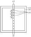
도 2는 종래의 파워라인 배치 구조를 나타내는 도면이다.2 is a view showing a conventional power line arrangement structure.
도 2를 참조하면, 종래의 파워라인(power line)은 감지 증폭기 영역(103) 내에 수직 방향으로 배치되는 다수개의 제1 파워 라인(M1 power line)(210)과 메모리 셀(101) 및 서브 워드 드라이버 영역(105)에 수평방향으로 배치되는 다수개의 제2 파워 라인(M2 power line)(220, 230, 240)으로 나뉜다. 여기서, 제1 파워 라 인(210)은 제2 파워 라인(220, 230, 240)의 하부에 위치하게 된다. 즉, 반도체 장치(100)에 필요한 전원을 공급하는 파워 라인(power line)은 2단 구조를 갖는 것이다.Referring to FIG. 2, a conventional power line includes a plurality of
파워 라인(power line)을 통하여 공급되는 전압의 레벨은 다양하게 존재한다. VP는 높은 전원 전압 레벨을 가리키며, VSS는 낮은 전원 전압 레벨을 가리킨다. VSSA는 코아로 들어가는 낮은 전원 전압 레벨을 가리킨다. VINTA는 메모리 셀(코아 셀)로 입력되는 내부 전압(Intermal Voltage)을 뜻한다. 그리고, VBL은 비트라인을 프리차지 시키는 전압 레벨을 뜻한다. 파워 라인을 통하여 공급되는 서로 다른 전압 레벨의 개수는 가변적이다. 즉, 반도체 장치를 구동시키기 위하여 필요한 전압 레벨들에 따라, 서로 다른 값을 가지는 전압 레벨의 개수가 정해지는 것이다.There are various levels of voltage supplied through the power line. VP indicates a high supply voltage level and VSS indicates a low supply voltage level. VSSA refers to the low supply voltage level entering the core. VINTA is an internal voltage input to a memory cell (core cell). VBL is a voltage level for precharging the bit line. The number of different voltage levels supplied through the power lines is variable. That is, the number of voltage levels having different values is determined according to the voltage levels required for driving the semiconductor device.
반도체 장치를 구동시키기 위해서는, 일반적으로 낮은 전원 전압(VSS) 및 코아로 입력되는 낮은 전원 전압(VSSA), 높은 전원 전압(VP), 코아로 입력되는 내부 전압(VINTA), 비트라인 프리 차지 전압(VBL)이 요구된다. 따라서, 도 2에서는 상술한 전압 레벨들을 가지는 제1 파워 라인(M1 power line)들 및 제2 파워 라인(M2 power line)들을 도시하였다. 메모리 셀 영역(101)의 내에는 다수개의 데이터 입출력 라인(GIO: global Input/output)이 존재한다.In order to drive a semiconductor device, a low power supply voltage VSS and a low power supply voltage VSSA, a high power supply voltage VP, an internal voltage VINTA and a bit line precharge voltage VBL) is required. Accordingly, FIG. 2 illustrates first power lines M1 and second power lines M2 power lines having the above-described voltage levels. In the
그리고, 구비되는 파워 라인(power line)의 개수는 이용되는 반도체 장치의 메모리 용량 등에 따라서 달라진다. 예를 들어, 256MByte의 메모리 셀을 기준으로 했을 때, 메모리 셀(101) 영역에 수평방향으로 배치되는 제2 파워 라인(240)의 개 수는 1개 내지 3개가 된다. 그리고, 352MByte의 메모리 셀을 기준으로 하면, 메모리 셀(101) 영역에 수평 방향으로 배치되는 제2 파워 라인(240)의 개수는 7개가 될 수 있다. 따라서, 제작하고자 하는 메모리의 용량에 따라서, 구비되는 제1 또는 제2 파워 라인(M1, M2 power line)의 개수를 조절하면 된다.The number of power lines provided varies depending on the memory capacity of the semiconductor device used. For example, based on 256 MByte memory cells, the number of
제1 파워 라인(210)은 감지 증폭기 영역(103)에 수직 방향으로 배치된다. 그리고, 제2 파워 라인(220, 230, 240)은 서브 워드 드라이버 영역(105) 및 메모리 셀 영역(101)에 수평방향으로 배치된다. 여기서, 종래의 반도체 장치에 있어서, 동일한 전압 레벨을 가지는 제1 파워 라인(210)과 제2 파워 라인(220, 230, 240)은 비아(via)를 통하여 메쉬(mash) 되었다. 예를 들어, 제1 파워 라인(210)의 VP 전압 레벨을 갖는 파워 라인은, 제2 파워 라인(240)의 VP 전압 레벨을 갖는 파워 라인과 비아 컨택(via contact)을 통하여 접속되는 구조를 가졌다. 그리고, 종래의 파워라인 배치구조에서는 제2 파워라인(220, 230, 240)을 통하여 공급되는 전원들을 주 전원(main power)으로 사용하였다.The
메모리 셀 영역(101)에 수직 방향으로는 워드라인 인에이블 신호 라인(NWE)(250)이 배치된다. 워드라인 인에이블 신호 라인(NWE)(250)은 제1 파워 라인(210)이 배치되는 층 또는 제2 파워 라인(220, 230, 240)이 배치되는 층, 또는 다른 층에 배치될 수 있다. 워드라인 인에이블 신호 라인(250)은 반도체 장치의 디자인 룰(Design rule), 제작 공정 등에 따라 사용자가 특정 층에 배치되도록 하면 되는 것이다. 종래의 반도체 장치에 있어서, 메모리 셀 영역(101)의 내부에는 워드라인 인에이블 신호 라인(250)에 평행하게 수직방향으로 배치되는 파워 라인이 존 재하지 않았었다.A word line enable signal line (NWE) 250 is disposed in the vertical direction in the
도 2에 도시된 종래의 파워 라인 배치 구조는 메모리 셀 영역(101), 감지 증폭기 영역(105)에 수평 방향으로 배치되는 제2 파워 라인(220, 230, 240)을 주 전원 공급 라인(main power line)으로 한다. 그리고, 같은 레벨의 전압을 인가받는 제1 파워 라인과 제2 파워 라인이 교차하는 261, 263, 265 지점 비아 컨택(via contact)이 형성되었다. 제2 파워 라인을 통해 공급되는 전압을 비아 컨택을 통하여 제1 파워 라인(210)으로 공급되는 구조를 가진 것이다.In the conventional power line arrangement shown in FIG. 2, the main power supply line includes the
비아 컨택이 많으면 많을수록, 전원을 공급하는데 있어서 발생하는 노이즈가 줄어들게 된다. 그러나, 상술한 종래의 배치 구조는 메모리 셀 영역(101)내에는 별도의 파워 라인이 구비되지 않았다. 그리고, 셀 영역(101)에서는 비아 컨택(via contact)이 존재하지 않았다. 따라서, 종래의 배치구조는 노이즈(noise)의 분산 효과가 떨어지는 문제가 있다.The more via contacts there are, the less noise there is in providing power. However, the conventional arrangement structure described above does not include a separate power line in the
그리고, 데이터 입출력 라인(GIO line)이 증가하는 경우 제2 파워 라인(240)들을 데이터 입출력 라인으로 이용하기도 하였다. 따라서, 데이터 입출력 라인(GIO line)이 증가하는 경우, 각각의 입출력 라인(GIO line) 하나에 전달되는 파워 용량(전원 용량)이 감소하였다. 즉, 파워 공급 능력이 감소되는 단점이 있는 것이다. 이러한, 파워 공급 능력의 취약은 반도체 장치의 동작 속도(speed)를 떨어뜨리고, 이는 수율감소로 이어지게 된다.In addition, when the data input / output line (GIO line) increases, the
상술한 2단 구조(제1 파워라인 및 제2 파워라인을 갖는 2개의 층에 존재하는 파워라인을 통해서 파워 공급)가 갖는 파워 취약의 문제점을 해결하기 위하여, 3단 구조를 갖는 파워 라인 구조(미도시)가 도입되었다.In order to solve the problem of power weakness of the above-described two-stage structure (power supply through the power lines existing in two layers having the first power line and the second power line), the power line structure having the three-stage structure ( Not shown).
그러나, 3단 구조를 갖는 파워 라인 구조는 파워 공급면에서는 우수하나, 이는 별도의 파워 라인 메탈 층(M3 power line)을 필요로 하므로 반도체 장치의 제작 비용 및 공정상의 어려움 등이 발생하는 문제가 있다. 또한, 3단 구조에서는 반도체 칩의 크기(size) 및 공정에서의 제작 시간 또한 증가하게 되는 단점이 있다.However, although the power line structure having the three-stage structure is excellent in terms of power supply, it requires a separate power line metal layer (M3 power line), which causes problems such as manufacturing cost and difficulty in manufacturing a semiconductor device. . In addition, the three-stage structure has a disadvantage in that the size of the semiconductor chip and the manufacturing time in the process also increase.
따라서, 칩 크기 및 제작 비용을 최소화하면서, 파워 공급 효율 및 노이즈 발생면에서 우수한 성능을 가지는 파워 라인 구조가 필요하다.Accordingly, there is a need for a power line structure having excellent performance in terms of power supply efficiency and noise generation while minimizing chip size and manufacturing cost.
본 발명이 이루고자하는 기술적 과제는 파워 공급 효율이 우수한 파워라인 배치 구조를 제공하는데 있다.The technical problem to be achieved by the present invention is to provide a power line arrangement structure excellent in power supply efficiency.
상기 기술적 과제를 달성하기 위한 본 발명의 일 실시예에 따른 파워 라인 배치 구조는 제1 영역 및 제2 영역을 구비한다.The power line arrangement structure according to the embodiment of the present invention for achieving the above technical problem has a first region and a second region.
제1 영역은 메모리 셀 영역 및 서브 워드라인 드라이버 영역에 있어서, 워드라이 인에이블 신호 라인들 사이에 평행 배치되는 다수개의 제1 파워 라인들이 배치된다.In the first region, the memory cell region and the sub wordline driver region may include a plurality of first power lines arranged in parallel between the word enable signal lines.
제2 영역은 메모리 셀 영역 및 서브 워드라인 드라이버 영역에 있어서, 상기 제1 파워 라인의 수직 방향으로 배치되는 다수개의 제2 파워 라인들이 배치된다.In the second region, the memory cell region and the sub wordline driver region may include a plurality of second power lines arranged in a vertical direction of the first power line.
제1 영역은 제2 영역의 하부에 구비되는 것을 특징으로 하며, 서로 동일한 전압 레벨을 갖는 제1 및 제2 파워 라인들은 메쉬되어 있다.The first region is provided under the second region, and the first and second power lines having the same voltage level are meshed with each other.
여기서, 메쉬는 비아를 이용하여, 서로 동일한 전압 레벨을 갖는 제1 및 제2 파워 라인을 접속시킴으로써 이루어진다.Here, the mesh is made by connecting first and second power lines having the same voltage level to each other using vias.
본 발명의 다른 실시예에 따른 파워 라인 배치 구조는 제1 영역, 제2 영역, 및 플레이트 폴리를 구비한다.A power line arrangement in accordance with another embodiment of the present invention includes a first region, a second region, and a plate pulley.
제1 영역에는 메모리 셀 영역 및 서브 워드라인 드라이버 영역에 있어서, 워드라이 인에이블 신호 라인들 사이에 평행하게 배치되는 다수개의 제1 파워 라인들이 구비된다.The first region includes a plurality of first power lines disposed in parallel between word-enabled signal lines in the memory cell region and the sub-wordline driver region.
제2 영역에는 메모리 셀 영역에 있어서, 상기 제1 영역 상부에 배치되며, 상기 제1 파워 라인에 수직하여 배치된다.In the second region, the memory cell region is disposed above the first region, and is disposed perpendicular to the first power line.
플레이트 폴리는 상기 제1 영역의 하부에 구비된다. 서로 동일한 전압 레벨을 갖는 상기 제1 및 제2 파워 라인들은 메쉬되며, 상기 제1 파워 라인들 중 바이어스 전압을 공급받는 제1 파워 라인은 상기 플레이트 폴리와 메탈 컨택으로 접속된다.Plate pulleys are provided below the first region. The first and second power lines having the same voltage level are meshed with each other, and a first power line supplied with a bias voltage among the first power lines is connected to the plate poly by a metal contact.
상기 기술적 과제를 달성하기 위한 본 발명의 다른 실시예에 따른 파워 라인 배치 구조는 제1 영역, 제2 영역, 및 제3 영역을 구비한다.According to another aspect of the present invention, there is provided a power line arrangement structure including a first region, a second region, and a third region.
제1 영역에는 메모리 셀 영역 및 서브 워드라인 드라이버 영역에 있어서, 워드라이 인에이블 신호 라인들 사이에 평행하게 배치되는 다수개의 제1 파워 라인들이 구비된다.The first region includes a plurality of first power lines disposed in parallel between word-enabled signal lines in the memory cell region and the sub-wordline driver region.
제2 영역에는 메모리 셀 영역에 있어서, 상기 제1 영역 상부에 배치되며, 상기 제1 파워 라인에 수직하여 배치된다.In the second region, the memory cell region is disposed above the first region, and is disposed perpendicular to the first power line.
제3 영역에는 메모리 셀 영역에 있어서, 상기 제1 파워 라인과 동일 방향으로 배치되는 다수개의 제3 파워 라인들이 구비된다.The third area includes a plurality of third power lines arranged in the same direction as the first power line in the memory cell area.
상기 제1 영역은 상기 제2 영역의 하부에 구비되며, 상기 제2 영역은 상기 제3 영역의 하부에 구비된다.The first area is provided below the second area, and the second area is provided below the third area.
서로 동일한 전압 레벨을 갖는 상기 제1 및 제2 파워 라인들은 메쉬되고, 서로 동일한 전압 레벨을 갖는 상기 제2 및 제3 파워 라인들은 메쉬된다.The first and second power lines having the same voltage level as each other are meshed, and the second and third power lines having the same voltage level as each other are meshed.
본 발명과 본 발명의 동작상의 이점 및 본 발명의 실시에 의하여 달성되는 목적을 충분히 이해하기 위해서는 본 발명의 바람직한 실시예를 예시하는 첨부 도면 및 도면에 기재된 내용을 참조하여야 한다.DETAILED DESCRIPTION In order to fully understand the present invention, the operational advantages of the present invention, and the objects achieved by the practice of the present invention, reference should be made to the accompanying drawings which illustrate preferred embodiments of the present invention and the contents described in the drawings.
이하, 첨부한 도면을 참조하여 본 발명이 바람직한 실시예를 설명함으로써, 본 발명을 상세히 설명한다. 각 도면에 제시된 동일한 참조부호는 동일한 부재를 나타낸다.Hereinafter, exemplary embodiments of the present invention will be described in detail with reference to the accompanying drawings. Like reference numerals in the drawings denote like elements.
도 3은 본 발명의 일 실시예에 따른 파워라인 배치 구조를 개략적으로 나타내는 도면이다.3 is a diagram schematically illustrating a power line arrangement structure according to an embodiment of the present invention.
도 3을 참조하면, 본 발명에 따른 파워라인 배치 구조는 제1 파워라인(M1 power line)(350)이 배치되는 제1 영역, 및 제2 파워 라인(M2 power line)(325, 360)이 배치되는 제2 영역을 구비한다.Referring to FIG. 3, the power line arrangement structure according to the present invention includes a first region in which a
제1 영역은 메모리 셀 영역(320) 및 서브 워드 드라이버 영역(310)을 포함한다. 제1 파워 라인(350)은 메모리 셀 영역(320) 및 서브 워드 드라이버 영역(310) 내에서 수직 방향으로 배치되는 것이다.The first region includes a
제2 영역은 메모리 셀 영역(320)에 구비된다. 그리고, 서브 워드 드라이버 영역(310), 및 비트라인 감지 증폭기(미도시)를 더 포함할 수 있다. 제2 파워 라인(325, 360)은 메모리 셀 영역(320), 서브 워드 드라이버 영역(310), 및 비트라인 감지 증폭기(미도시) 내에서 수평 방향으로 배치되는 것이다.The second region is provided in the
여기서, 제2 파워 라인(325, 360)은 제1 파워 라인(350)의 상부에 배선된다. 그리고, 동일한 전압 레벨을 가지는 제1 및 제2 파워 라인들은 교차하는 곳(370, 375)에서, 비아(via)를 통하여 접속이 이루어진다. 비아(via)를 통하여 접속(contact)이 되는 구조를 메쉬(mesh) 구조라 한다. 예를 들어, 코아 셀(core cell)로 입력되는 낮은 전원 전압(VSSA) 레벨을 갖는 제2 파워 라인(325)은 370 지점에서 동일한 전압 레벨(VSSA)을 갖는 제1 파워 라인(350)과 교차된다. 370 지점에서 제1 및 제2 파워 라인은 비아(via)를 통해서 접속이 이루어지는 것이다.Here, the
본 발명에 따른 파워라인 배치 구조는 종래의 파워라인 배치 구조에 비하여 메모리 셀 영역(320) 내에 수직방향(워드라인 인에이블 신호 라인(NWE) 방향)으로 배치되는 다수개의 제1 파워라인들(350)을 더 구비한다. 따라서, 제2 파워라인(325, 360)들과 교차하는 지점(접속(contact)되는 지점)도 증가하게 된다.The power line arrangement according to the present invention has a plurality of
제2 파워 라인(325, 360)을 주 전원(main power) 공급 라인으로 한다면, 제2 파워 라인(325, 360)과 제1 파워 라인의 교차 지점에 발생하는 접속 지점(contact)이 증가하게 한다. 접속 지점이 많을수록 저항성분이 분산되어 저항이 감소하게 되며, 노이즈(noise)의 분산 효과가 증가하게 된다. 그리고, 데이터 입출력 라인(GIO)이 증가하더라도, 제1 파워 라인을 이용한 파워의 보강이 이루어질 수 있 다. 따라서, 전원 공급 효율을 높일 수 있는 효과가 발생하는 것이다.If the
도 4는 도 3에 따른 파워 라인 배치 구조를 상세히 나타내는 도면이다.4 is a view showing in detail the power line arrangement structure according to FIG.
도 4를 참조하면, 본원의 제1 파워 라인(470)은 워드라인 인에이블 신호 라인들(490)이 배열된 방향(수직 방향)으로 배열된다. 그리고, 인접한 두 개의 워드라인 인에이블 신호 라인들(490) 사이에, 일정 간격씩 이격되어 배치된다.Referring to FIG. 4, the
도 4에 도시된 입출력 신호 라인(GIO) 및 각각의 전압 레벨 표시(VINTA, VSSA, VP, VBL 등)는 도 2에서 설명한 바와 동일하다.The input / output signal lines GIO and respective voltage level indications VINTA, VSSA, VP, VBL, etc. shown in FIG. 4 are the same as described in FIG.
동일한 전압 레벨을 가지는 제1 파워 라인(470)과 제2 파워 라인(450, 460)이 교차되는 지점에서 접속(contact)이 이뤄지는 것은 작은 원으로 도시되어 있다. 도시된 바와 같이, 본 발명에 따른 파워 라인 배치 구조는 메모리 셀 영역(320) 내에 워드 라인 인에이블 신호 라인(490)과 평행하게 배치되는 제1 파워 라인(470)을 구비함으로써, 메모리 셀 영역(320)에 다수개의 접속 지점(contact)들을 가질 수 있다.The contact made at the point where the
여기서, 감지 증폭기 영역(430)내에 존재하는 수직 방향으로 배열된 제1 파워 라인(470)들은 종래의 감지 증폭기내 배치된 파워 라인과 동일하다. 따라서, 감지 증폭기 영역(480)에 배치된 제1 파워라인(480)들의 자세한 설명은 생략한다.Here, the
제2 파워라인(450, 460)은 메모리 셀 영역(320) 및 서브 워드 드라이버 영역(310)에 수평 ??향(워드라인 인에이블 신호 라인(490)에 수직한 방향)으로 배치된다.The
가장 높은 전압 레벨을 가지는 높은 전원 전압(VP) 레벨의 제1 파워 라 인(472)은 메모리 셀 영역(320)의 정 가운데에 배치되는 것이 바람직하다. 높은 전원 전압(VP)은 전송하는 파워 량이 가장 크므로, 각 셀의 중앙에 하나씩 배치되도록 하는 것이다.The
제1 파워라인(470, 480)은 제2 파워 라인(450, 460)의 하단에 구비된다. 본 발명에 따른 파워라인 배치 구조는 2단으로 구성되는 것이다. 따라서, 3단으로 파워 라인 배치 구조를 형성하지 않고도, 저항의 감소에 따른 노이즈의 분산효과, 파워 공급 능력의 향상을 가져올 수 있다. 즉, 제1 파워 라인(470)들을 셀 영역(320)에 배치하고, 제2 파워 라인(460)과 메쉬 구조를 형성시킴으로써, 셀 영역의 파워를 보강할 수 있다.The
여기서, 제1 또는 제2 파워라인들의 개수는 이용되는 반도체 장치의 메모리 용량, 동작 속도(speed) 등에 따라서 달라진다. 따라서, 제작자는 제작하고자 하는 메모리의 사양에 따라서, 구비되는 제1 또는 제2 파워 라인(M1, M2 power line)의 개수를 조절하면 되는 것이다.Here, the number of first or second power lines depends on the memory capacity, operating speed, etc. of the semiconductor device used. Therefore, the manufacturer may adjust the number of first or second power lines M1 and M2 provided in accordance with the specification of the memory to be manufactured.
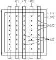
도 5a는 본 발명의 다른 실시예에 따른 파워라인 배치 구조를 나타내는 도면이다.5A is a diagram illustrating a power line arrangement structure according to another embodiment of the present invention.
도 5a를 참조하면, 본 발명의 다른 실시예에 따른 파워라인 배치 구조(500)는 도 4의 배치구조에 비하여 플레이트 폴리(PP: plate poly)(510)를 더 구비한다. 셀 영역(320)에 배치되는 하나의 제1 파워라인(472)은 플레이트 폴리(510)와 메탈 컨택(MC: metal contact)(520)을 형성한다. 여기서, 매탈 컨택이 형성되는 제1 파워라인(472)은 바이어스 전압(bias voltage)을 인가받는 파워라인이 된다. 여기서, 메탈 컨택(520)이란, 일정 기판(예를 들어, 플레이트 폴리) 위에 메탈 라인(예를 들어 472 제1 파워라인)이 배선될 때, 일정 간격마다 접속 지점을 형성시키고, 접속 지점을 금속 물질로 채우는 것으로, 당업자에게 자명한 것이라 할 것이다.5A, the
그리고, 나머지 제1 파워 라인들(471, 473, 470) 또한 플레이트 폴리(510)와 메탈 컨택(520)을 통하여 접속될 수 있다.The remaining
여기서, 바이어스 전압은 VP 전압 값을 갖는 것이 바람직하다. 바이어스 전압은 전체 전압을 바이어싱(biasing)하기 위한 것이다.Here, the bias voltage preferably has a VP voltage value. The bias voltage is for biasing the total voltage.
또한, 바이어스 전압을 인가받는 제1 파워 라인(472)은 셀의 중심에 위치하도록 하는 것이 바람직하다.In addition, the
도 5a에서 도시된 바와 같이, 본 발명의 다른 실시예에 따른 배치구조(500)는 제1 파워 라인들(471, 472, 473, 470)과 플레이트 폴리(510)를 메탈 컨택(520)을 이용해 접속시킴으로써, 전원 공급에 따라 발생하는 노이즈를 감소시킬 수 있다. 나아가, 안정적인 전원 공급을 할 수 있는 효과가 있다.As shown in FIG. 5A, the
도 5b는 도 5a의 플레이트 폴리와 바이어스 전압을 인가받는 제1 파워 라인의 컨택을 상세히 나타내는 도면이다.FIG. 5B is a diagram illustrating in detail a contact of the plate pull of FIG. 5A and a first power line to which a bias voltage is applied. FIG.
도 5b를 참조하면, 바이어스 전압을 인가받는 제1 파워라인(472)과 플레이트 폴리(510) 사이에는 일정 간격(d)으로 메탈 컨택(520)이 형성된다. 메탈 컨택(520)은 여기서, 일정 간격(d)은 반도체 장치의 디자인 룰(disign rule)에 따라서 달라진다. 디자인 룰(disign rule)이 허용하는 한 상기 간격 d를 줄이고, 메탈 컨택(520)의 개수를 증가시키면, 노이즈 분산 효과를 더 증대시킬 수 있다.Referring to FIG. 5B, a
도 5c는 도 5a의 플레이트 폴리와 제1 파워 라인들의 컨택을 상세히 나타내는 도면이다.5C is a view illustrating in detail the contact of the plate pulley and the first power lines of FIG. 5A.
제1 파워 라인(471, 472, 473)들 모두가 플레이트 폴리(510)와 메탈 컨택(520)을 통하여 접속되도록 할 수 있다.All of the
제1 파워 라인들과 플레이트 폴리(510)를 매탈 컨택을 이용해 전기적으로 접속(contact)시킴으로써, 상술한 노이즈 분산 효과의 극대화를 가져올 수 있다.By electrically contacting the first power lines and the
도 6a는 도 5a의 워드라인 배치 및 여분의 워드라인 구비를 상세히 나타내는 도면이다.FIG. 6A is a diagram illustrating in detail the word line arrangement and spare word lines of FIG. 5A.
256cell 구조, 512cell 구조, 또는 1024cell 구조와 같은 경우, 여분의 워드라인이 발생하지 않는다. 여기서, 여분의 워드라인이란, 구비된 워드라인들 중 직접적으로 워드라인으로 이용되는 않는 것을 뜻한다. 256cell 구조, 512cell 구조, 또는 1024cell 구조에 있어서 여분의 워드라인이 발생하지 않는 것은 본 발명이 속하는 기술분야에서 통상의 지식을 가진 자에게 있어서 자명하다 할 것이다. 또한 320cell, 640cell 구조와 같은 경우에는 여분의 워드라인이 발생하게 된다. 즉, 구비된 워드라인들이 모두 워드라인으로 이용되지 않고, 남는 라인들이 발생한다.In the case of a 256 cell structure, a 512 cell structure, or a 1024 cell structure, no extra word lines are generated. Here, the redundant word line means that the word lines are not directly used among the provided word lines. It will be apparent to those skilled in the art that an extra word line does not occur in a 256 cell structure, a 512 cell structure, or a 1024 cell structure. In the case of 320 cell and 640 cell structures, an extra word line is generated. That is, not all the provided word lines are used as word lines, and remaining lines are generated.
도 3, 도 4, 및 도 5a에서는 워드라인(490)이 1개씩 이격하여 구비되는 경우를 도시하였으나, 워드라인은 일정 묶음개씩 구비될 수 있다. 즉, 도 6a를 참조하면, 두개 이상의 워드라인들(예를 들어, 3개(601, 603))이 한 개의 묶음으로 구비될 수 있다.3, 4, and 5A illustrate the case where the word lines 490 are spaced one by one, the word lines may be provided in a predetermined bundle. That is, referring to FIG. 6A, two or more word lines (eg, three (601, 603)) may be provided in one bundle.
본 발명에서는, 셀의 구조상 여분의 워드라인이 발생하지 않는 경우, 추가적 인 워드라인을 구비시킨다. 그리고, 추가된 워드라인을 데이터 신호 라인(GIO) 또는 제1 파워 라인으로써 이용한다. 셀 구조상 여분의 워드라인이 발생하는 경우, 남는 워드라인을 데이터 신호라인(GIO) 또는 제1 파워 라인으로써 이용한다. 여기서, 상기 추가된 워드라인 또는 상기 남는 워드라인을 dummy 워드라인이라 한다.In the present invention, if an extra word line does not occur due to the structure of the cell, an additional word line is provided. The added word line is used as the data signal line GIO or the first power line. When an extra word line occurs in the cell structure, the remaining word line is used as the data signal line GIO or the first power line. Here, the added word line or the remaining word line is called a dummy word line.
도 6a를 참조하면, dummy 워드라인을 블록 당 워드라인을 한개 또는 그 이상개씩 추가되는 파워라인 배치구조가 도시된다. 즉, 061, 603, 및 607은 dummy 워드라인들이고, 나머지 603 워드라인들은 직접적으로 워드라인으로 이용되는 라인들이다.Referring to FIG. 6A, a power line arrangement structure in which dummy word lines are added one or more word lines per block is shown. That is, 061, 603, and 607 are dummy word lines, and the remaining 603 word lines are lines used directly as word lines.
도 6b는 도 5a의 워드라인 배치 및 여분의 워드라인 구비를 상세히 나타내는 도면이다.FIG. 6B is a diagram illustrating in detail the word line arrangement and redundant word lines of FIG. 5A.
도 6b를 참조하면, dummy 워드라인들은 셀(320)의 한쪽에 몰아서 구비하는 경우가 도시되어 있다. 즉, 650 부분에 dummy 워드라인이 배치되도록 하는 것이다. 나머지 490 부분에는 직접적으로 워드라인으로 이용되는 라인들이 배치되어 있다.Referring to FIG. 6B, a case where dummy word lines are provided on one side of the
도 6a 및 도 6b에서 예시된 배치구조 이외에도 여분의 워드라인(dummy wordline)이 배치되는 위치는 매우 다양하게 존재할 수 있으며, 이는 자명하다 할 것이다.In addition to the arrangement structure illustrated in FIGS. 6A and 6B, positions where redundant wordlines are arranged may exist in a wide variety of ways, which will be apparent.
도 7은 본 발명의 다른 실시예에 따른 파워라인 배치 구조를 나타내는 도면이다.7 is a view showing a power line arrangement according to another embodiment of the present invention.
도 7을 참조하면, 도 5a의 배치구조에 제 3영역을 더 구비시킬 수 있다. 제3 영역은 제2 파워라인들의 상위층에 구비되는 영역이다. 즉, 제3 영역은 셀 영 역(320)의 상부에 존재한다. 그리고, 서브 워드라인 드라이버 영역(450) 및/또는 감지 증폭기 영역(430)을 더 포함할 수 있다. 제3 영역에는 제3 파워라인들(710)이 배치된다. 제3 파워라인들(720)은 도시된 바와 같이 제1 파워라인들(471, 472, 473)이 배치된 방향과 동일 방향으로 배치된다.Referring to FIG. 7, a third region may be further provided in the arrangement of FIG. 5A. The third area is an area provided above the second power lines. That is, the third region exists above the
그리고, 인가받는 전압값이 서로 같은 제2 파워 라인들(460) 및 제3 파워 라인들(710)은 서로 매쉬(mesh)된다. 즉, 비아 컨택(via contact)을 이용하여 접속되는 것이다. 나머지 구성들은 도 4 내지 도 6b에 도시된 바와 동일하므로, 상세한 설명은 생략하도록 한다.The
도 8은 도 5a 또는 도 6에서 구비되는 구성들의 수직방향 배치 순서를 나타내는 도면이다.FIG. 8 is a diagram illustrating a vertical arrangement order of components provided in FIG. 5A or 6.
도 8을 참조하면, 최하층에 플레이트 폴리(PP)(820)가 구비된다. 그리고 순차로, 메탈 컨택(810), 제1 파워라인(801), 비아 컨택(811), 제2 파워라인(803), 비아 컨택(813), 및 제3 파워라인(805)이 각각 적층된다.Referring to FIG. 8, a plate poly (PP) 820 is provided at a lowermost layer. The
이상에서와 같이 도면과 명세서에서 최적 실시예가 개시되었다. 여기서 특정한 용어들이었으나, 이는 단지 본 발명을 설명하기 위한 목적에서 사용된 것이지 의미한정이나 특허청구범위에 기재된 본 발명의 범위를 제한하기 위하여 사용된 것은 아니다. 그러므로 본 기술분야의 통상의 지식을 가진 자라면 이로부터 다양한 변형 및 균등한 타 실시예가 가능하다는 점을 이해할 것이다. 따라서, 본 발명의 진정한 기술적 보호범위는 첨부된 특허청구범위의 기술적 사상에 의해 정해져야 할 것이다.As described above, optimal embodiments have been disclosed in the drawings and the specification. Although specific terms have been used herein, these terms are only used for the purpose of describing the present invention and are not intended to limit the scope of the present invention as defined in the claims or the claims. Therefore, those skilled in the art will understand that various modifications and equivalent other embodiments are possible therefrom. Therefore, the true technical protection scope of the present invention will be defined by the technical spirit of the appended claims.
상술한 바와 같이 본 발명에 따른 파워 라인 배치 구조는 반도체 칩 면적 및 제작비용을 최소화하면서도 파워 공급 능력을 향상시키고 저항발생에 따른 노이즈를 감소시킬 수 있는 장점이 있다.As described above, the power line arrangement structure according to the present invention has an advantage of improving power supply capability and reducing noise due to resistance while minimizing semiconductor chip area and manufacturing cost.
Claims (31)
Translated fromKoreanPriority Applications (1)
| Application Number | Priority Date | Filing Date | Title |
|---|---|---|---|
| US11/979,868US7808804B2 (en) | 2006-11-10 | 2007-11-09 | Power line layout |
Applications Claiming Priority (2)
| Application Number | Priority Date | Filing Date | Title |
|---|---|---|---|
| KR1020060111224 | 2006-11-10 | ||
| KR20060111224 | 2006-11-10 |
Publications (2)
| Publication Number | Publication Date |
|---|---|
| KR20080042655Atrue KR20080042655A (en) | 2008-05-15 |
| KR100885920B1 KR100885920B1 (en) | 2009-02-26 |
Family
ID=39649325
Family Applications (1)
| Application Number | Title | Priority Date | Filing Date |
|---|---|---|---|
| KR1020070052198AActiveKR100885920B1 (en) | 2006-11-10 | 2007-05-29 | Power Line Arrangement Structure of Semiconductor Device |
Country Status (1)
| Country | Link |
|---|---|
| KR (1) | KR100885920B1 (en) |
Cited By (1)
| Publication number | Priority date | Publication date | Assignee | Title |
|---|---|---|---|---|
| KR20180095173A (en)* | 2017-02-17 | 2018-08-27 | 에스케이하이닉스 주식회사 | Semiconductor memory device including power mesh structure |
Families Citing this family (3)
| Publication number | Priority date | Publication date | Assignee | Title |
|---|---|---|---|---|
| KR101157024B1 (en)* | 2010-09-03 | 2012-06-21 | 에스케이하이닉스 주식회사 | Semiconductor Integrated Circuit |
| KR102161736B1 (en) | 2014-08-13 | 2020-10-05 | 삼성전자주식회사 | System on chip, electronic apparatus including system on chip and design method of system on chip |
| KR102472376B1 (en) | 2017-10-16 | 2022-12-01 | 에스케이하이닉스 주식회사 | Three dimensional semiconductor memory device |
Family Cites Families (2)
| Publication number | Priority date | Publication date | Assignee | Title |
|---|---|---|---|---|
| KR100319627B1 (en)* | 1999-06-12 | 2002-01-05 | 김영환 | Semiconductor memory apparatus |
| KR100676200B1 (en)* | 2004-12-14 | 2007-01-30 | 삼성전자주식회사 | Memory cell array, memory device, and plate voltage supply method having plate voltage insensitive to noise |
- 2007
- 2007-05-29KRKR1020070052198Apatent/KR100885920B1/enactiveActive
Cited By (1)
| Publication number | Priority date | Publication date | Assignee | Title |
|---|---|---|---|---|
| KR20180095173A (en)* | 2017-02-17 | 2018-08-27 | 에스케이하이닉스 주식회사 | Semiconductor memory device including power mesh structure |
Also Published As
| Publication number | Publication date |
|---|---|
| KR100885920B1 (en) | 2009-02-26 |
Similar Documents
| Publication | Publication Date | Title |
|---|---|---|
| US7808804B2 (en) | Power line layout | |
| TWI620196B (en) | Flying-and interleaved bit line architecture for dual-strip static random access memory (DP-SRAM) | |
| US7391636B2 (en) | Semiconductor memory device and arrangement method thereof | |
| KR20250022083A (en) | Sub-wordline driver | |
| US5263002A (en) | Semiconductor memory device and its topography | |
| JPH02154391A (en) | semiconductor storage device | |
| US20150055393A1 (en) | Semiconductor Device Having Multi-Level Wiring Structure | |
| KR100885920B1 (en) | Power Line Arrangement Structure of Semiconductor Device | |
| US6317353B1 (en) | Semiconductor integrated circuit | |
| US6288927B1 (en) | Semiconductor memory device with column gate and equalizer circuitry | |
| JP4901515B2 (en) | Ferroelectric semiconductor memory device | |
| US7242602B2 (en) | Semiconductor memory devices having conductive line in twisted areas of twisted bit line pairs | |
| EP0788109B1 (en) | Semiconductor integrated circuit having improved wiring in input terminal | |
| KR20030043410A (en) | Semiconductor memory device having structure for minimizing coupling between global input/output lines | |
| US9443573B2 (en) | Semiconductor device including main amplifers between memory cell arrays | |
| JP2004110979A (en) | DRAM circuit and operation method thereof | |
| JPS6386186A (en) | semiconductor storage device | |
| JP3972509B2 (en) | Semiconductor memory device, semiconductor device using the same, and electronic equipment | |
| KR20120087665A (en) | Semiconductor memory apparatus | |
| US20030235096A1 (en) | High density mask ROM having flat-type bank select | |
| JP4063502B2 (en) | DRAM memory | |
| KR100702007B1 (en) | Semiconductor memory device and signal line arrangement method thereof | |
| KR960001462B1 (en) | Dynamic semiconductor memory device | |
| JP2003324160A (en) | Semiconductor memory device | |
| KR100204537B1 (en) | A semiconductor memory device having subword line and strap structure |
Legal Events
| Date | Code | Title | Description |
|---|---|---|---|
| A201 | Request for examination | ||
| PA0109 | Patent application | Patent event code:PA01091R01D Comment text:Patent Application Patent event date:20070529 | |
| PA0201 | Request for examination | ||
| PG1501 | Laying open of application | ||
| E902 | Notification of reason for refusal | ||
| PE0902 | Notice of grounds for rejection | Comment text:Notification of reason for refusal Patent event date:20080529 Patent event code:PE09021S01D | |
| AMND | Amendment | ||
| E601 | Decision to refuse application | ||
| PE0601 | Decision on rejection of patent | Patent event date:20080905 Comment text:Decision to Refuse Application Patent event code:PE06012S01D Patent event date:20080529 Comment text:Notification of reason for refusal Patent event code:PE06011S01I | |
| AMND | Amendment | ||
| J201 | Request for trial against refusal decision | ||
| PJ0201 | Trial against decision of rejection | Patent event date:20081006 Comment text:Request for Trial against Decision on Refusal Patent event code:PJ02012R01D Patent event date:20080905 Comment text:Decision to Refuse Application Patent event code:PJ02011S01I Appeal kind category:Appeal against decision to decline refusal Decision date:20081209 Appeal identifier:2008101010337 Request date:20081006 | |
| PB0901 | Examination by re-examination before a trial | Comment text:Amendment to Specification, etc. Patent event date:20081006 Patent event code:PB09011R02I Comment text:Request for Trial against Decision on Refusal Patent event date:20081006 Patent event code:PB09011R01I Comment text:Amendment to Specification, etc. Patent event date:20080728 Patent event code:PB09011R02I | |
| B701 | Decision to grant | ||
| PB0701 | Decision of registration after re-examination before a trial | Patent event date:20081209 Comment text:Decision to Grant Registration Patent event code:PB07012S01D Patent event date:20081106 Comment text:Transfer of Trial File for Re-examination before a Trial Patent event code:PB07011S01I | |
| GRNT | Written decision to grant | ||
| PR0701 | Registration of establishment | Comment text:Registration of Establishment Patent event date:20090220 Patent event code:PR07011E01D | |
| PR1002 | Payment of registration fee | Payment date:20090223 End annual number:3 Start annual number:1 | |
| PG1601 | Publication of registration | ||
| PR1001 | Payment of annual fee | Payment date:20120131 Start annual number:4 End annual number:4 | |
| FPAY | Annual fee payment | Payment date:20130131 Year of fee payment:5 | |
| PR1001 | Payment of annual fee | Payment date:20130131 Start annual number:5 End annual number:5 | |
| FPAY | Annual fee payment | Payment date:20140129 Year of fee payment:6 | |
| PR1001 | Payment of annual fee | Payment date:20140129 Start annual number:6 End annual number:6 | |
| FPAY | Annual fee payment | Payment date:20150202 Year of fee payment:7 | |
| PR1001 | Payment of annual fee | Payment date:20150202 Start annual number:7 End annual number:7 | |
| PR1001 | Payment of annual fee | Payment date:20210128 Start annual number:13 End annual number:13 | |
| PR1001 | Payment of annual fee | Payment date:20220126 Start annual number:14 End annual number:14 | |
| PR1001 | Payment of annual fee | Payment date:20230125 Start annual number:15 End annual number:15 | |
| PR1001 | Payment of annual fee | Payment date:20250124 Start annual number:17 End annual number:17 |