KR20080041458A - Internal Clock Generation Circuit and Data Driver Using It - Google Patents
Internal Clock Generation Circuit and Data Driver Using ItDownload PDFInfo
- Publication number
- KR20080041458A KR20080041458AKR1020060109578AKR20060109578AKR20080041458AKR 20080041458 AKR20080041458 AKR 20080041458AKR 1020060109578 AKR1020060109578 AKR 1020060109578AKR 20060109578 AKR20060109578 AKR 20060109578AKR 20080041458 AKR20080041458 AKR 20080041458A
- Authority
- KR
- South Korea
- Prior art keywords
- internal clock
- voltage
- bias voltage
- bias
- clock signal
- Prior art date
- Legal status (The legal status is an assumption and is not a legal conclusion. Google has not performed a legal analysis and makes no representation as to the accuracy of the status listed.)
- Withdrawn
Links
Images


Classifications
- H—ELECTRICITY
- H03—ELECTRONIC CIRCUITRY
- H03K—PULSE TECHNIQUE
- H03K5/00—Manipulating of pulses not covered by one of the other main groups of this subclass
- H03K5/22—Circuits having more than one input and one output for comparing pulses or pulse trains with each other according to input signal characteristics, e.g. slope, integral
- H03K5/24—Circuits having more than one input and one output for comparing pulses or pulse trains with each other according to input signal characteristics, e.g. slope, integral the characteristic being amplitude
- H03K5/2472—Circuits having more than one input and one output for comparing pulses or pulse trains with each other according to input signal characteristics, e.g. slope, integral the characteristic being amplitude using field effect transistors
- H03K5/2481—Circuits having more than one input and one output for comparing pulses or pulse trains with each other according to input signal characteristics, e.g. slope, integral the characteristic being amplitude using field effect transistors with at least one differential stage
- G—PHYSICS
- G09—EDUCATION; CRYPTOGRAPHY; DISPLAY; ADVERTISING; SEALS
- G09G—ARRANGEMENTS OR CIRCUITS FOR CONTROL OF INDICATING DEVICES USING STATIC MEANS TO PRESENT VARIABLE INFORMATION
- G09G3/00—Control arrangements or circuits, of interest only in connection with visual indicators other than cathode-ray tubes
- G09G3/20—Control arrangements or circuits, of interest only in connection with visual indicators other than cathode-ray tubes for presentation of an assembly of a number of characters, e.g. a page, by composing the assembly by combination of individual elements arranged in a matrix no fixed position being assigned to or needed to be assigned to the individual characters or partial characters
- G09G3/34—Control arrangements or circuits, of interest only in connection with visual indicators other than cathode-ray tubes for presentation of an assembly of a number of characters, e.g. a page, by composing the assembly by combination of individual elements arranged in a matrix no fixed position being assigned to or needed to be assigned to the individual characters or partial characters by control of light from an independent source
- G09G3/36—Control arrangements or circuits, of interest only in connection with visual indicators other than cathode-ray tubes for presentation of an assembly of a number of characters, e.g. a page, by composing the assembly by combination of individual elements arranged in a matrix no fixed position being assigned to or needed to be assigned to the individual characters or partial characters by control of light from an independent source using liquid crystals
- G—PHYSICS
- G02—OPTICS
- G02F—OPTICAL DEVICES OR ARRANGEMENTS FOR THE CONTROL OF LIGHT BY MODIFICATION OF THE OPTICAL PROPERTIES OF THE MEDIA OF THE ELEMENTS INVOLVED THEREIN; NON-LINEAR OPTICS; FREQUENCY-CHANGING OF LIGHT; OPTICAL LOGIC ELEMENTS; OPTICAL ANALOGUE/DIGITAL CONVERTERS
- G02F1/00—Devices or arrangements for the control of the intensity, colour, phase, polarisation or direction of light arriving from an independent light source, e.g. switching, gating or modulating; Non-linear optics
- G02F1/01—Devices or arrangements for the control of the intensity, colour, phase, polarisation or direction of light arriving from an independent light source, e.g. switching, gating or modulating; Non-linear optics for the control of the intensity, phase, polarisation or colour
- G02F1/13—Devices or arrangements for the control of the intensity, colour, phase, polarisation or direction of light arriving from an independent light source, e.g. switching, gating or modulating; Non-linear optics for the control of the intensity, phase, polarisation or colour based on liquid crystals, e.g. single liquid crystal display cells
- G02F1/133—Constructional arrangements; Operation of liquid crystal cells; Circuit arrangements
- G—PHYSICS
- G09—EDUCATION; CRYPTOGRAPHY; DISPLAY; ADVERTISING; SEALS
- G09G—ARRANGEMENTS OR CIRCUITS FOR CONTROL OF INDICATING DEVICES USING STATIC MEANS TO PRESENT VARIABLE INFORMATION
- G09G3/00—Control arrangements or circuits, of interest only in connection with visual indicators other than cathode-ray tubes
- G09G3/20—Control arrangements or circuits, of interest only in connection with visual indicators other than cathode-ray tubes for presentation of an assembly of a number of characters, e.g. a page, by composing the assembly by combination of individual elements arranged in a matrix no fixed position being assigned to or needed to be assigned to the individual characters or partial characters
- G09G3/34—Control arrangements or circuits, of interest only in connection with visual indicators other than cathode-ray tubes for presentation of an assembly of a number of characters, e.g. a page, by composing the assembly by combination of individual elements arranged in a matrix no fixed position being assigned to or needed to be assigned to the individual characters or partial characters by control of light from an independent source
- G09G3/36—Control arrangements or circuits, of interest only in connection with visual indicators other than cathode-ray tubes for presentation of an assembly of a number of characters, e.g. a page, by composing the assembly by combination of individual elements arranged in a matrix no fixed position being assigned to or needed to be assigned to the individual characters or partial characters by control of light from an independent source using liquid crystals
- G09G3/3611—Control of matrices with row and column drivers
- H—ELECTRICITY
- H03—ELECTRONIC CIRCUITRY
- H03K—PULSE TECHNIQUE
- H03K3/00—Circuits for generating electric pulses; Monostable, bistable or multistable circuits
- H03K3/02—Generators characterised by the type of circuit or by the means used for producing pulses
- H03K3/023—Generators characterised by the type of circuit or by the means used for producing pulses by the use of differential amplifiers or comparators, with internal or external positive feedback
- H—ELECTRICITY
- H03—ELECTRONIC CIRCUITRY
- H03K—PULSE TECHNIQUE
- H03K3/00—Circuits for generating electric pulses; Monostable, bistable or multistable circuits
- H03K3/02—Generators characterised by the type of circuit or by the means used for producing pulses
- H03K3/353—Generators characterised by the type of circuit or by the means used for producing pulses by the use, as active elements, of field-effect transistors with internal or external positive feedback
- H03K3/356—Bistable circuits
- G—PHYSICS
- G09—EDUCATION; CRYPTOGRAPHY; DISPLAY; ADVERTISING; SEALS
- G09G—ARRANGEMENTS OR CIRCUITS FOR CONTROL OF INDICATING DEVICES USING STATIC MEANS TO PRESENT VARIABLE INFORMATION
- G09G2300/00—Aspects of the constitution of display devices
- G09G2300/04—Structural and physical details of display devices
- G09G2300/0421—Structural details of the set of electrodes
- G09G2300/0426—Layout of electrodes and connections
- G—PHYSICS
- G09—EDUCATION; CRYPTOGRAPHY; DISPLAY; ADVERTISING; SEALS
- G09G—ARRANGEMENTS OR CIRCUITS FOR CONTROL OF INDICATING DEVICES USING STATIC MEANS TO PRESENT VARIABLE INFORMATION
- G09G2310/00—Command of the display device
- G09G2310/02—Addressing, scanning or driving the display screen or processing steps related thereto
- G09G2310/0264—Details of driving circuits
- G09G2310/027—Details of drivers for data electrodes, the drivers handling digital grey scale data, e.g. use of D/A converters
- G—PHYSICS
- G09—EDUCATION; CRYPTOGRAPHY; DISPLAY; ADVERTISING; SEALS
- G09G—ARRANGEMENTS OR CIRCUITS FOR CONTROL OF INDICATING DEVICES USING STATIC MEANS TO PRESENT VARIABLE INFORMATION
- G09G2310/00—Command of the display device
- G09G2310/08—Details of timing specific for flat panels, other than clock recovery
- G—PHYSICS
- G09—EDUCATION; CRYPTOGRAPHY; DISPLAY; ADVERTISING; SEALS
- G09G—ARRANGEMENTS OR CIRCUITS FOR CONTROL OF INDICATING DEVICES USING STATIC MEANS TO PRESENT VARIABLE INFORMATION
- G09G2330/00—Aspects of power supply; Aspects of display protection and defect management
- G09G2330/02—Details of power systems and of start or stop of display operation
- G—PHYSICS
- G09—EDUCATION; CRYPTOGRAPHY; DISPLAY; ADVERTISING; SEALS
- G09G—ARRANGEMENTS OR CIRCUITS FOR CONTROL OF INDICATING DEVICES USING STATIC MEANS TO PRESENT VARIABLE INFORMATION
- G09G2330/00—Aspects of power supply; Aspects of display protection and defect management
- G09G2330/06—Handling electromagnetic interferences [EMI], covering emitted as well as received electromagnetic radiation
- G—PHYSICS
- G09—EDUCATION; CRYPTOGRAPHY; DISPLAY; ADVERTISING; SEALS
- G09G—ARRANGEMENTS OR CIRCUITS FOR CONTROL OF INDICATING DEVICES USING STATIC MEANS TO PRESENT VARIABLE INFORMATION
- G09G2370/00—Aspects of data communication
- G09G2370/08—Details of image data interface between the display device controller and the data line driver circuit
- G—PHYSICS
- G09—EDUCATION; CRYPTOGRAPHY; DISPLAY; ADVERTISING; SEALS
- G09G—ARRANGEMENTS OR CIRCUITS FOR CONTROL OF INDICATING DEVICES USING STATIC MEANS TO PRESENT VARIABLE INFORMATION
- G09G3/00—Control arrangements or circuits, of interest only in connection with visual indicators other than cathode-ray tubes
- G09G3/20—Control arrangements or circuits, of interest only in connection with visual indicators other than cathode-ray tubes for presentation of an assembly of a number of characters, e.g. a page, by composing the assembly by combination of individual elements arranged in a matrix no fixed position being assigned to or needed to be assigned to the individual characters or partial characters
- G09G3/34—Control arrangements or circuits, of interest only in connection with visual indicators other than cathode-ray tubes for presentation of an assembly of a number of characters, e.g. a page, by composing the assembly by combination of individual elements arranged in a matrix no fixed position being assigned to or needed to be assigned to the individual characters or partial characters by control of light from an independent source
- G09G3/36—Control arrangements or circuits, of interest only in connection with visual indicators other than cathode-ray tubes for presentation of an assembly of a number of characters, e.g. a page, by composing the assembly by combination of individual elements arranged in a matrix no fixed position being assigned to or needed to be assigned to the individual characters or partial characters by control of light from an independent source using liquid crystals
- G09G3/3611—Control of matrices with row and column drivers
- G09G3/3648—Control of matrices with row and column drivers using an active matrix
Landscapes
- Physics & Mathematics (AREA)
- Engineering & Computer Science (AREA)
- General Physics & Mathematics (AREA)
- Chemical & Material Sciences (AREA)
- Crystallography & Structural Chemistry (AREA)
- Computer Hardware Design (AREA)
- Theoretical Computer Science (AREA)
- Nonlinear Science (AREA)
- Mathematical Physics (AREA)
- Optics & Photonics (AREA)
- Control Of Indicators Other Than Cathode Ray Tubes (AREA)
Abstract
Translated fromKoreanDescription
Translated fromKorean도 1은 본 발명의 일실시예에 따른 액정 표시 장치를 도시한 도면,1 is a view showing a liquid crystal display device according to an embodiment of the present invention;
도 2는 도 1의 데이터 드라이버를 도시한 도면,2 is a diagram illustrating a data driver of FIG. 1;
도 3은 도 2의 RSDS 수신부를 도시한 예시 회로도,3 is an exemplary circuit diagram illustrating an RSDS receiver of FIG. 2;
도 4는 도 2의 RSDS 수신부의 내부 클럭 생성부의 다른 실시예를 도시한 도면이다.FIG. 4 is a diagram illustrating another embodiment of an internal clock generator of the RSDS receiver of FIG. 2.
<도면의 주요부분에 대한 부호설명><Code Description of Main Parts of Drawing>
100: 액정 표시 장치 110: 액정 패널100: liquid crystal display 110: liquid crystal panel
120: 데이터 드라이버 122: RSDS 수신부120: data driver 122: RSDS receiver
130: 게이트 드라이버 140: 타이밍 컨트롤러130: gate driver 140: timing controller
144: RSDS 송신부 210: 바이어스 전압 공급부144: RSDS transmitter 210: bias voltage supply
212: 정전압부 214: 전류 싱크부212: constant voltage section 214: current sink section
220: 내부 클럭 생성부 222: 정전류부220: internal clock generation unit 222: constant current unit
224: 차동 증폭부 230: 바이어스 라인224: differential amplifier 230: bias line
240: 쉴드 라인240: shield line
본 발명은 액정 표시 장치에 관한 것으로서, 특히 액정 표시 장치의 내부 클럭 생성 회로 및 그것을 이용하는 데이터 드라이버에 관한 것이다.The present invention relates to a liquid crystal display device, and more particularly, to an internal clock generation circuit of a liquid crystal display device and a data driver using the same.
일반적으로 액정 표시 장치는 전계 생성 전극이 각각 형성된 박막 트랜지스터 기판과 컬러 필터 기판을 전극이 형성된 면이 마주 대하도록 배치하고 두 기판 사이에 액정을 주입한 후, 전극에 전압을 인가하여 생성되는 전기장에 의해 액정을 움직이게 함으로써, 이에 따라 달라지는 빛의 투과율에 의해 화상을 표현하는 장치이다.In general, a liquid crystal display device includes a thin film transistor substrate and a color filter substrate each having a field generating electrode disposed so that the surface on which the electrode is formed face each other, injecting a liquid crystal between the two substrates, and then applying a voltage to the electrode to generate an electric field. By moving the liquid crystal by this, it is an apparatus for representing the image by the transmittance of light that varies accordingly.
이러한 액정 표시 장치는, 데이터 라인과 게이트 라인의 교차 영역에 형성된 복수의 액정 셀을 포함하는 액정 패널, 데이터 라인에 데이터 신호를 인가하는 데이터 드라이버, 게이트 라인에 게이트 구동 신호를 인가하는 게이트 드라이버, 데이터 드라이버와 게이트 드라이버를 제어하는 타이밍 컨트롤러 및 액정 패널의 구동 전압을 공급하는 전원 공급부를 포함한다.Such a liquid crystal display includes a liquid crystal panel including a plurality of liquid crystal cells formed at an intersection region of a data line and a gate line, a data driver for applying a data signal to the data line, a gate driver for applying a gate driving signal to the gate line, and data A timing controller for controlling the driver and the gate driver, and a power supply for supplying a driving voltage of the liquid crystal panel.
전원 공급부는 외부로부터 입력되는 데이터 신호를 액정 패널에 표시하기 위하여 데이터 드라이버, 게이트 드라이버 및 타이밍 컨트롤러 등에 전원 전압(VDD), 접지 전압(VSS) 등 액정 표시 장치를 구동시키기 위한 구동 전압을 공급한다.The power supply unit supplies a driving voltage for driving the liquid crystal display, such as a power supply voltage VDD and a ground voltage VSS, to a data driver, a gate driver, and a timing controller to display a data signal input from the outside on the liquid crystal panel.
그런데 종래 전원 공급부로부터 구동 전압을 공급받아 구동하는 데이터 드라이버는 노이즈(Noise)에 의해 전원 전압(VDD)에 리플(Ripple)이 발생할 경우 내부 클럭의 생성이 지연되어 액정 패널에 비정상적인 화면이 표시되는 문제점이 있다.However, in the case of a data driver driven by a driving voltage supplied from a conventional power supply, when a ripple occurs in the power supply voltage VDD due to noise, generation of an internal clock is delayed and an abnormal screen is displayed on the liquid crystal panel. There is this.
본 발명이 이루고자 하는 기술적 과제는 인터페이스 수신부의 바이어스 라인을 쉴드하는 쉴드 라인에 바이어스 전압을 인가하여 바이어스 라인과 쉴드 라인 사이에 발생하는 기생 커패시턴스를 제거하는 내부 클럭 생성 회로 및 그것을 이용한 데이터 드라이버를 제공하는 데 있다.SUMMARY OF THE INVENTION The present invention provides an internal clock generation circuit for removing parasitic capacitance generated between a bias line and a shield line by applying a bias voltage to a shield line shielding a bias line of an interface receiver, and a data driver using the same. There is.
상기 목적을 달성하기 위하여 본 발명의 내부 클럭 생성 회로는, 전원 전압을 공급받아 바이어스 전압을 생성하는 바이어스 전압 공급부; 바이어스 전압에 응답하여 차동 클럭 신호를 내부 클럭 신호로 변환하여 출력하는 내부 클럭 생성부; 상기 바이어스 전압 공급부와 상기 내부 클럭 생성부를 전기적으로 연결하고 상기 바이어스 전압을 전달하는 바이어스 라인; 및 상기 바이어스 라인을 실드하며, 상기 바이어스 전압이 인가되는 쉴드 라인을 포함한다.In order to achieve the above object, the internal clock generation circuit of the present invention includes a bias voltage supply unit configured to generate a bias voltage by receiving a power supply voltage; An internal clock generator configured to convert the differential clock signal into an internal clock signal and output the internal clock signal in response to a bias voltage; A bias line electrically connecting the bias voltage supply unit and the internal clock generator to transfer the bias voltage; And a shield line shielding the bias line and to which the bias voltage is applied.
여기서 상기 쉴드 라인은 상기 바이어스 라인에 이격되며 상기 바이어스 라인에 수평하게 형성되는 것이 바람직하다.The shield line may be spaced apart from the bias line and formed horizontally on the bias line.
또한 상기 바이어스 전압 공급부는, 상기 전원 전압을 상기 바이어스 전압으 로 출력하는 정전압부; 및 인에이블 신호에 응답하여 상기 정전압부에 접지 전압을 인가하는 전류 싱크부를 포함한다.The bias voltage supply unit may include a constant voltage unit configured to output the power supply voltage as the bias voltage; And a current sink for applying a ground voltage to the constant voltage unit in response to the enable signal.
또한 상기 전류 싱크부는 접지 전압을 인에이블 신호로 입력받는 것이 바람직하다.In addition, the current sink unit preferably receives the ground voltage as an enable signal.
또한 상기 내부 클럭 생성부는, 상기 바이어스 전압에 응답하여 정전류를 생성하는 정전류부, 및 상기 정전류에 의해 인에이블되어 상기 차동 클럭 신호를 상기 내부 클럭 신호로 변환하여 출력하는 차동 증폭부를 포함한다.The internal clock generation unit may include a constant current unit configured to generate a constant current in response to the bias voltage, and a differential amplifier unit that is enabled by the constant current and converts the differential clock signal into the internal clock signal.
또한 상기 차동 증폭부는 크로스 커플된 두 개의 모스 트랜지스터를 포함하며, 상기 두 개의 모스 트랜지스터는 크기가 동일한 것이 바람직하다.In addition, the differential amplification unit includes two MOS transistors cross-coupled, and the two MOS transistors are preferably the same size.
또한 상기 차동 증폭부는 다이오드 연결을 가지는 제1 모스 트랜지스터와 상기 제1 모스 트랜지스터와 전류 미러 타입으로 결합되는 제2 모스 트랜지스터를 포함한다.The differential amplifier may include a first MOS transistor having a diode connection and a second MOS transistor coupled to the first MOS transistor in a current mirror type.
본 발명의 데이터 드라이버는 데이터 시작 신호에 응답하여 내부 클럭 신호를 샘플링하는 쉬프트 레지스터; 데이터 신호를 상기 샘플링된 내부 클럭에 동기시켜 저장하는 입력 레지스터; 로드 신호에 응답하여 상기 입력 레지스터에 저장된 데이터를 동시에 저장하는 저장 레지스터; 상기 저장 레지스터에 저장된 데이터를 감마 전압을 이용하여 아날로그 전압으로 변환하는 디지털 아날로그 변환기; 상기 아날로그 전압을 해당 데이터 라인에 동시에 출력하는 출력 버퍼; 및 외부로부터 입력되는 차동 클럭 신호를 상기 내부 클럭 신호로 변환하여 출력하는 인터페이스 수신부;를 포함하며, 상기 인터페이스 수신부는 전원 전압을 공급받아 바이어스 전 압을 생성하는 바이어스 전압 공급부; 바이어스 전압에 응답하여 차동 클럭 신호를 내부 클럭 신호로 변환하여 출력하는 내부 클럭 생성부; 상기 바이어스 전압 공급부와 상기 내부 클럭 생성부를 전기적으로 연결하고 상기 바이어스 전압을 전달하는 바이어스 라인; 및 상기 바이어스 라인을 실드하며, 상기 바이어스 전압이 인가되는 쉴드 라인을 포함한다.A data driver of the present invention includes a shift register for sampling an internal clock signal in response to a data start signal; An input register configured to store a data signal in synchronization with the sampled internal clock; A storage register for simultaneously storing data stored in the input register in response to a load signal; A digital analog converter for converting data stored in the storage register into an analog voltage using a gamma voltage; An output buffer for simultaneously outputting the analog voltage to a corresponding data line; And an interface receiver for converting the differential clock signal input from the outside into the internal clock signal and outputting the internal clock signal, wherein the interface receiver includes a bias voltage supply unit configured to generate a bias voltage by receiving a power supply voltage; An internal clock generator configured to convert the differential clock signal into an internal clock signal and output the internal clock signal in response to a bias voltage; A bias line electrically connecting the bias voltage supply unit and the internal clock generator to transfer the bias voltage; And a shield line shielding the bias line and to which the bias voltage is applied.
이하, 첨부한 도면을 참조하여 본 발명의 바람직한 일 실시예에 대해 상세히 설명한다.Hereinafter, with reference to the accompanying drawings will be described in detail a preferred embodiment of the present invention.
도 1은 본 발명의 일실시예에 따른 액정 표시 장치를 도시한 도면이다. 도 1에 도시된 바와 같이, 본 발명의 일실시예에 따른 액정 표시 장치(100)는 액정 패널(110), 데이터 드라이버(120), 게이트 드라이버(130), 타이밍 컨트롤러(140) 및 전원 공급부(150)를 포함한다.1 is a diagram illustrating a liquid crystal display according to an exemplary embodiment of the present invention. As shown in FIG. 1, the liquid
상기 액정 패널(110)은 컬러 필터가 형성된 상부 기판, 박막 트랜지스터가 형성된 하부 기판 및 상부 기판과 하부 기판 사이에 충진되는 액정을 포함한다. 하부 기판은 게이트 라인(GL)과 데이터 라인(DL)의 교차부에 데이터 신호를 표시하는 액정 셀(Clc)과 게이트 구동 신호에 응답하여 데이터 신호를 액정셀(Clc)에 인가하는 박막 트랜지스터(TFT)가 형성된다. 박막 트랜지스터(TFT)는 게이트 라인(GL)에 연결되는 게이트, 데이터 라인(DL)에 연결되는 소스 및 액정셀(Clc)의 화소 전극에 연결되는 드레인을 포함한다.The
상기 데이터 드라이버(120)는 게이트 구동 신호에 의해 구동되는 박막 트랜 지스터(TFT)에 데이터 신호에 해당하는 아날로그 전압을 동시에 인가하여 게이트 라인(GL) 단위로 데이터 신호를 표시한다. 이를 위해 데이터 드라이버(120)는 타이밍 컨트롤러(140)로부터 제어신호, 데이터 신호를 공급받고, 전원 공급부(150)로부터 구동 전압을 인가받는다. 여기서 구동 전압은 전원 전압(VDD) 및 접지 전압(VSS)을 포함한다. 한편 데이터 드라이버(120)는 타이밍 컨트롤러(140)의 RSDS 송신부(142)에 대응되는 RSDS 수신부(122)를 포함한다.The
여기서 RSDS(Reduced Swing Differential Signaling)는 데이터 드라이버(120)가 타이밍 컨트롤러(140)로부터 제어 신호 및 데이터 신호를 전송받기 위한 인터페이스 방식이다. 본 실시예에서 타이밍 컨트롤러(140)와 데이터 드라이버(120) 간의 인터페이스 방식은 RSDS인 경우를 예시하여 설명하지만 타이밍 컨트롤러(140)와 데이터 드라이버(120) 간의 인터페이스 방식은 이에 한정되지 아니하며, LVDS(Low Voltage Differential Signaling), mini LVDS 또는 PPDS(Point-to-Point Differential Signaling) 일 수 있다.Here, reduced swing differential signaling (RSDS) is an interface scheme for the
상기 게이트 드라이버(130)는 복수의 게이트 라인(GL)에 순차적으로 게이트 구동 신호를 인가하여 게이트 라인(GL)에 연결된 복수의 박막 트랜지스터(TFT)를 동시에 턴온시킨다. 이를 위해 게이트 드라이버(120)는 타이밍 컨트롤러(140)로부터 제어신호를 공급받고, 전원 공급부(150)로부터 구동 전압을 인가받는다.The
상기 타이밍 컨트롤러(140)는 외부에서 입력되는 데이터 신호를 데이터 드라이버(120)가 처리할 수 있는 데이터 신호로 변환하여 데이터 드라이버(120)로 공급하고, 데이터 드라이버(120)와 게이트 드라이버(130)의 동작에 필요한 제어 신호를 데이터 드라이버(120)와 게이트 드라이버(130) 각각에 공급한다. 한편 타이밍 컨트롤러(140)는 데이터 드라이버(120)의 RSDS 수신부(122)에 대응되는 RSDS 송신부(142)를 포함한다. 여기서 데이터 드라이버(120)에 공급되는 데이터 신호는 R,G,B 데이터 신호이고 제어 신호는 차동 클럭 신호(CLKP,CLKN), 수평 동기 신호(HSYNC) 및 로드 제어 신호(LOAD)를 포함한다.The
상기 전원 공급부(150)는 데이터 드라이버(120), 게이트 드라이버(130) 등에 액정 표시 장치를 구동시키기 위한 구동 전압을 공급한다. 여기서 데이터 드라이버(120)에 공급되는 구동 전압은 전원 전압(VDD), 접지 전압(VSS) 및 감마 전압(VGAMMA)을 포함한다.The
도 2는 도 1의 데이터 드라이버를 도시한 도면이다. 도 2에 도시된 바와 같이, 본 발명의 일실시예에 따른 데이터 드라이버(120)는 쉬프트 레지스터(123), 입력 레지스터(124), 저장 레지스터(125), 디지털/아날로그 변환기(126), 출력 버퍼(127) 및 RSDS 수신부(122)를 포함한다.FIG. 2 is a diagram illustrating the data driver of FIG. 1. As shown in FIG. 2, the
보다 구체적으로 쉬프트 레지스터(123)는 데이터 시작 신호(STH)로 선택된 하나의 라인에 해당하는 모든 데이터 신호(R.G.B)를 내부 클럭(ICLK)에 동기시켜 입력 레지스터(124)에 샘플링한다. 입력 레지스터(124)에 저장된 하나의 라인에 해당하는 데이터 신호는 로드 제어신호(LOAD)에 의해 저장 레지스터(125)로 동시에 전달되어 저장된다. 저장 레지스터(125)에 저장된 데이터는 감마 전압(VGAMMA)에 의해 디지털/아날로그 변환기(126)에서 데이터 신호에 해당하는 아날로그 전압으로 변환되어 출력 버퍼(127)로 입력된다. 출력 버퍼(127)는 해당 데이터 라인에 각각 해당 아날로그 전압을 동시에 출력한다.More specifically, the
상기 RSDS 수신부(122)는 타이밍 컨트롤러로부터 데이터 신호(R.G.B) 및 제어 신호(CLKP, CLKN, HSYNC)를 인가받아 쉬프트 레지스터(123) 및 입력 레지스터(124)가 처리할 수 있는 신호로 변환한다. 이를 위해 RSDS 수신부(122)는 전원 공급부로 부터 구동 전압(VDD, VSS)를 공급받는다.The
RSDS 수신부(122)는 데이터 신호(R.G.B)를 변환하는 입력 레지스터가 처리할 수 있는 데이터 신호로 변환하는 데이터 신호 변환 회로, 제어신호(HSYNC)를 쉬프트 레지스터를 제어할 수 있는 제어 신호(STH)로 변환하는 제어 신호 변환 회로 및 차동 클럭 신호(CLKP, CLKN)를 내부 클럭(ICLK)으로 변환하는 내부 클럭 생성 회로를 포함한다. 이하에서는 내부 클럭 생성 회로를 좀 더 자세하게 설명한다.The
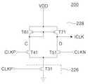
도 3은 도 2의 RSDS 수신부의 내부 클럭 생성 회로를 예시한 도면이다. 도 3에 도시된 바와 같이, RSDS 수신부의 내부 클럭 생성 회로(200)는 바이어스 전압 공급부(210), 내부 클럭 생성부(220), 바이어스 라인(230) 및 쉴드 라인(240)을 포함한다.3 is a diagram illustrating an internal clock generation circuit of the RSDS receiver of FIG. 2. As illustrated in FIG. 3, the internal
상기 바이어스 전압 공급부(210)는 전원 전압(VDD)을 공급받아 내부 클럭 생성부(220)에 일정한 바이어스 전압(VBIAS)을 인가한다. 구체적으로 바이어스 전압 공급부(210)는 전원 전압(VDD)을 바이어스 전압(VBIAS)으로 출력하는 정전압부(212)와 인에이블 신호(ENABLE)에 응답하여 정전압부(212)에 접지 전압(VSS)을 인가하는 전류 싱크부(214)를 포함한다.The bias
정전압부(212)는 전원 전압(VDD)이 인가되는 드레인, 드레인에 공통 연결되고 바이어스 라인(230)에 연결되어 바이어스 전압(VBIAS)을 출력하는 게이트, 전류 싱크부(214)에 연결되는 소스를 포함하는 다이오드 형태의 NMOS 트랜지스터(T1)일 수 있다. 전류 싱크부(214)는 정전압부(212)의 소스에 연결되는 드레인, 인에이블 신호(ENABLE)가 인가되는 게이트 및 접지 전압(VSS)이 인가되는 소스를 포함하는 NMOS 트랜지스터(T2)일 수 있다.The
상기 내부 클럭 생성부(220)는 바이어스 라인(230)을 통하여 인가되는 바이어스 전압(VBIAS)에 응답하여 타이밍 컨트롤러로부터 입력되는 차동 클럭 신호(CLKP, CLKN)를 내부 클럭 신호(ICLK)로 출력한다. 구체적으로 내부 클럭 생성부(220)는 바이어스 전압(VBIAS)에 응답하여 일정한 전류를 차동 증폭부(224)로 공급하는 정전류부(222)와 정전류부(222)로부터 일정한 전류를 공급받아 차동 클럭 신호(CLKP, CLKN)를 내부 클럭 신호(ICLK)로 생성하여 데이터 드라이버의 쉬프트 레지스터로 출력하는 차동 증폭부(224)를 포함한다.The
정전류부(222)는 전원 전압(VDD)이 인가되는 드레인, 바이어스 라인(230)에 연결되어 바아어스 전압(VBIAS)이 인가되는 게이트, 차동 증폭부(224)에 연결되는 소스를 포함하는 NMOS 트랜지스터(T3)일 수 있다.The constant
차동 증폭부(224)는 차동 클럭 신호(CLKP, CLKN)를 입력받는 NMOS 트랜지스터(T4, T5), 드레인과 게이트가 서로 크로스 커플(Cross Couple)된 NMOS 트랜지스터(T6, T7)를 포함한다. NMOS 트랜지스터 T4, T5는 드레인이 정전류부(222)의 소스 에 연결되고, 게이트로 차동 클럭 신호 CLKP, CLKN가 각각 입력되며, 소스가 NMOS 트랜지스터 T6, T7의 드레인에 각각 연결된다. NMOS 트랜지스터 T4와 T5는 동일한 크기의 트랜지스터인 것이 바람직하다. NMOS 트랜지스터 T6, T7은 드레인이 NMOS 트랜지스터 T4, T5의 소스에 각각 연결되며, 게이트가 서로의 드레인에 각각 크로스 커플되어 연결되고, 소스에 접지 전압(VSS)가 인가되도록 그라운드에 연결된다. 여기서 NMOS 트랜지스터(T4)의 소스와 NMOS 트랜지스터(T6)의 드레인이 연결된 노드 A는 차동 증폭부(224)의 출력단으로 동작한다.The
상기 바이어스 라인(230)은 바이어스 전압 공급부(210)와 내부 클럭 생성부(220)를 전기적으로 연결하고, 바이어스 전압 공급부(210)의 바이어스 전압(VBIAS)을 내부 클럭 생성부(220)로 전달한다. 구체적으로 바이어스 라인(230)은 바이어스 전압 공급부(210)의 출력단, 즉 정전압부(212)의 NMOS 트랜지스터 T1의 게이트에 연결되며, 내부 클럭 생성부(220)의 입력단, 즉 정전류부(222)의 NMOS 트랜지스터 T3의 게이트에 연결된다.The
상기 쉴드 라인(240)은 바이어스 라인(230)에 인가된 바이어스 전압(VBIAS)을 안정화하기 위해 바이어스 라인(230)에 이격되어 수평 방향으로 형성된다. 쉴드 라인(240)은 바이어스 라인(230)이 형성된 기판의 동일 평면상에 바이어스 라인(230)을 쉴드 하도록 좌우로 두 라인이 형성될 수 있다. 또한 바이어스 라인(230)이 형성된 기판이 다층(Multi-Layer)으로 형성된 경우 바이어스 라인(230)을 쉴드 하도록 상하로 두 라인이 형성될 수 있다. 기판 쉴드 라인(240)에는 바이어스 라인(230)에 인가된 바이어스 전압(VBIAS)이 인가되는 것이 바람직하다. 본 실시예에서 바이어스 전압(VBIAS)은 전원 전압(VDD)이므로 쉴드 라인(240)에는 전원 전압(VDD)이 인가된다.The
이하 RSDS 수신부의 내부 클럭 생성 회로의 동작 과정을 설명한다.Hereinafter, an operation process of the internal clock generation circuit of the RSDS receiver will be described.
먼저 바이이스 전압 공급부(210)의 동작을 설명한다. 인에이블 신호(ENABLE)가 "하이" 레벨로 인가된 경우, 전류 싱크부(214)의 NMOS 트랜지스터 T2는 턴온되어 그라운드에 연결된다. 정전압부(212)는 드레인과 게이트가 공통으로 연결된 다이오드 구조를 가지므로 NMOS 트랜지스터 T1의 문턱 전압 이상인 전원 전압(VDD)이 드레인에 인가되면 턴온된다. 따라서 전원 전압(VDD)이 인가된 드레인으로부터 그라운드를 연결하는 경로(Path)가 형성되고 형성된 경로를 따라 전류가 흐른다. 이때 바이어스 전압 공급부(210)에서 출력되는 바이어스 전압(VBIAS)은 접지 전압(VSS) 레벨이 된다.First, the operation of the vise
인에이블 신호(ENABLE)가 "로우" 레벨로 인가된 경우, 전류 싱크부(214)의 NMOS 트랜지스터 T2는 턴오프되어 그라운드와 연결이 차단된다. 따라서 전원 전압(VDD)이 인가된 드레인으로부터 그라운드를 연결하는 경로(Path)가 차단되어 전류가 흐르지 않는다. 이때 바이어스 전압 공급부(210)에서 출력되는 바이어스 전압(VBIAS)은 전원 전압(VDD) 레벨이 된다.When the enable signal ENABLE is applied at the "low" level, the NMOS transistor T2 of the
여기서 인에이블 신호(ENABLE)는 "로우" 레벨의 전압, 예를 들면 접지 전압(VSS)일 수 있다. 인에이블 신호(ENABLE)로 "로우"레벨의 전압이 인가되면, 바이어스 전압 공급부(212)는 항상 전원 전압(VDD) 레벨의 바이어스 전압(VBIAS)을 내 부 클럭 생성부(220)로 인가할 수 있다.The enable signal ENABLE may be a "low" level voltage, for example, the ground voltage VSS. When the voltage of the "low" level is applied as the enable signal ENABLE, the bias
다음으로 내부 클럭 생성부(220)의 동작을 설명한다. 바이어스 전압 공급부(210)로부터 바이어스 전압(VBIAS)이 인가되면, 정전류부(222)는 턴온되어 차동 증폭부(224)로 일정한 전류를 공급하여 차동 증폭부(224)를 인에이블 시킨다. 차동 클럭 신호 CLKP가 "하이" 레벨로 인가된 경우 NMOS 트랜지스터 T4는 턴온되어 노드 A의 전위를 상승시킨다. 노드 A에 게이트가 연결된 트랜지스터 T7은 턴온되어 노드 B를 그라운드에 연결시킨다. 이때 차동 클럭 신호 CLKN은 "로우" 레벨로 인가되어 노드 B의 전위를 상승시킬 수 있는 NMOS 트랜지스터 T5를 턴오프시킨다. 따라서 노드 B는 접지 전압(VSS) 레벨의 전위를 가지며, 노드 B에 게이트가 연결된 트랜지스터 T6는 턴오프되어 노드 A의 전위를 유지시킨다. 즉 차동 클럭 신호 CLKP가 "하이" 레벨로 인가된 경우 노드 A에 연결된 출력단은 "하이" 레벨의 내부 클럭(ICLK)을 출력한다.Next, the operation of the
차동 클럭 신호 CLKN이 "하이" 레벨로 인가된 경우 NMOS 트랜지스터 T5는 턴온되어 노드 B의 전위를 상승시킨다. 노드 B에 게이트가 연결된 트랜지스터 T6은 턴온되어 노드 A를 그라운드에 연결시킨다. 이때 차동 클럭 신호 CLKP는 "로우" 레벨로 인가되어 노드 A의 전위를 상승시킬 수 있는 NMOS 트랜지스터 T4를 턴오프시킨다. 따라서 노드 A는 접지 전압(VSS) 레벨의 전위를 가지며, 노드 A에 게이트가 연결된 트랜지스터 T7은 턴오프되어 노드 B의 전위를 유지시킨다. 즉 차동 클럭 ㅅ신호 CLKP가 "로우" 레벨로 인가된 경우 노드 A에 연결된 출력단은 "로우" 레벨의 내부 클럭(ICLK)을 출력한다. 상술한 동작을 통하여 내부 클럭 신호 생성부(220)는 차동 클럭 신호(CLKP, CLKN)로부터 내부 클럭(ICLK)를 생성한다.When the differential clock signal CLKN is applied at the "high" level, the NMOS transistor T5 is turned on to raise the potential of Node B. Transistor T6, gated at node B, is turned on to connect node A to ground. The differential clock signal CLKP is then applied to the "low" level to turn off the NMOS transistor T4, which can raise the potential of node A. Therefore, node A has a potential at the ground voltage (VSS) level, and transistor T7 having a gate connected to node A is turned off to maintain the potential of node B. That is, when the differential clock signal CLKP is applied at the "low" level, the output terminal connected to the node A outputs the internal clock ICLK at the "low" level. Through the above-described operation, the internal
다음으로 전원 전압(VDD)에 리플이 발생하는 경우 바이어스 라인(230)과 쉴드 라인(240)의 상호 관계에 대하여 설명한다. 본 발명의 일실시예에 따르는 경우 바이어스 라인(230)과 쉴드 라인(240)에는 동일한 레벨의 전압, 즉 바이어스 전압(VBIAS)이 인가되는 구조를 가진다. 따라서 전원 전압(VDD)에 리플(Ripple)이 발생하는 경우에도 바이어스 전압 공급부(210)는 내부 클럭 생성부(220)로 안정하게 바이어스 전압(VBIAS)을 인가할 수 있다. 이를 좀 더 자세하게 설명한다.Next, when the ripple occurs in the power supply voltage VDD, the relationship between the
만약 전원 전압(VDD)에 리플이 발생하는 경우 바이어스 라인(230)에 인가되는 바이어스 전압(VBIAS)과 동시에 내부 클럭 생성부(220)에 공급되는 전원 전압(VDD)에도 함께 리플이 발생하기 때문에 전원 전압(VDD)에 발생된 리플은 내부 클럭 생성부(220)의 내부 클럭 생성에 영향을 미치지 않는다. 또한 바이어스 라인(230)과 쉴드 라인(240)에 동일한 레벨의 전압이 인가되므로 전원 전압(VDD)에 생성된 리플이 감소되는 경우에 바이어스 라인(230)과 쉴드 라인(240)에 기생 커패시턴시에 의한 영향이 발생되지 않는다.If a ripple occurs in the power supply voltage VDD, a ripple also occurs in the power supply voltage VDD supplied to the
본 발명의 일실시예와는 달리 바이어스 라인(230)에 인가되는 바이어스 전압(VBIAS)과 다른 레벨의 전압을 쉴드 라인(240)에 인가하면, 전원 전압(VDD)에 리플이 감소하는 경우 바이어스 라인(230)과 쉴드 라인(240)간에 형성된 기생 커패시턴스에 의해 바이어스 전압(VBIAS)의 레벨이 흔들리게 되고, 이로 인해 내부 클럭 생성부(220)의 정전류부(222)는 일정한 전류를 차동 증폭부(224)로 공급할 수 없게 되어 내부 클럭(ICLK) 생성의 지연이 발생된다.Unlike the exemplary embodiment of the present invention, when a voltage having a different level from the bias voltage VBIAS applied to the
도 4는 도 2의 RSDS 수신부의 내부 클럭 생성부의 다른 실시예를 도시한 도면이다. 도 4에 도시된 바와 같이, 다른 실시예에 따른 RSDS 수신부의 내부 클럭 생성부(220)는 전류 미러(Current Mirror)형 차동 증폭부(228)와 그라운드에 연결된 정전류부(226)를 포함한다.FIG. 4 is a diagram illustrating another embodiment of an internal clock generator of the RSDS receiver of FIG. 2. As illustrated in FIG. 4, the
차동 증폭부(228)는 게이트가 어느 하나의 드레인에 공통 연결된 전류 미러형의 PMOS 트랜지스터(T61, T71)와 차동 클럭 신호(CLKP, CLKN)를 입력받는 NMOS 트랜지스터(T41, T51)를 포함한다. PMOS 트랜지스터 T61, T71는 소스에 전원 전압(VDD)이 인가되고, 게이트가 PMOS 트랜지스터 T61의 드레인에 공통 연결되며, 드레인이 NMOS 트랜지스터 T41, T51의 드레인에 각각 연결된다. NMOS 트랜지스터 T41, T51은 드레인이 PMOS 트랜지스터 T61, T71의 드레인에 각각 연결되며, 게이트에 차동 클럭 신호 CLKP, CLKN가 각각 입력되며, 소스에 정전류부(226)가 연결된다. NMOS 트랜지스터 T41와 T51은 동일한 크기의 트랜지스터인 것이 바람직하다.The
정전류부(226)는 드레인이 차동 증폭부(228)의 NMOS 트랜지스터 T41, T51의 소스에 공통연결되고, 게이트에 바이어스 전압(VBIAS)이 인가되며, 소스에 접지 전압(VSS)이 인가되도록 그라운드에 연결된다. 여기서 PMOS 트랜지스터(T71)의 드레인과 NMOS 트랜지스터(T51)의 드레인이 연결된 노드 D는 차동 증폭부(228)의 출력단으로 동작한다.The constant
다음으로 본 발명의 다른 실시예에 따른 RSDS 수신부의 내부 클럭 생성부(220)의 동작을 설명한다. 바이어스 전압 공급부로부터 바이어스 전압(VBIAS)이 인가되면, 정전류부(226)의 NMOS 트랜지스터(T31)는 턴온되어 차동 증폭부(228)를 인에이블 시킨다. 차동 클럭 신호 CLKP가 "하이" 레벨로 인가된 경우 NMOS 트랜지스터 T41은 턴온되어, NMOS 트랜지스터 T31을 통하여 노드 C를 그라운드에 연결시킨다. 노드 C는 접지 전압(VSS) 레벨의 전위를 가지며, 노드 C에 게이트가 연결된 PMOS 트랜지스터 T71은 턴온되어 노드 D의 전위를 상승시킨다. 이때 차동 클럭 신호 CLKN은 "로우" 레벨로 인가되어 노드 D를 그라운드에 연결시킬 수 있는 NMOS 트랜지스터 T51를 턴오프시켜 노드 D의 전위를 유지시킨다. 즉 차동 클럭 신호 CLKP가 "하이" 레벨로 인가된 경우 노드 D에 연결된 출력단은 "하이" 레벨의 내부 클럭(ICLK)을 출력한다.Next, an operation of the
차동 클럭 신호 CLKN가 "하이" 레벨로 인가된 경우 NMOS 트랜지스터 T51은 턴온되어, NMOS 트랜지스터 T31을 통하여 노드 D를 그라운드에 연결시킨다. 노드 D는 접지 전압(VSS) 레벨의 전위를 가진다. 이때 차동 클럭 신호 CLKP은 "로우" 레벨로 인가되어 노드 C를 그라운드에 연결시킬 수 있는 NMOS 트랜지스터 T41를 턴오프시켜 노드 C의 전위를 유지시킨다. 즉 차동 클럭 신호 CLKP가 "로우" 레벨로 인가된 경우 노드 D에 연결된 출력단은 "로우" 레벨의 내부 클럭(ICLK)을 출력한다.When the differential clock signal CLKN is applied at the "high" level, the NMOS transistor T51 is turned on, connecting node D to ground through the NMOS transistor T31. Node D has a potential at ground voltage (VSS) level. At this time, the differential clock signal CLKP is applied to the "low" level to turn off the NMOS transistor T41, which can connect the node C to ground, to maintain the potential of the node C. That is, when the differential clock signal CLKP is applied at the "low" level, the output terminal connected to the node D outputs the internal clock ICLK at the "low" level.
상술한 동작을 통하여 내부 클럭 신호 생성부(220)는 차동 클럭 신호(CLKP, CLKN)로부터 내부 클럭(ICLK)를 생성한다.Through the above-described operation, the internal
본 발명의 내부 클럭 생성 회로 및 데이터 드라이버는, 인터페이스 수신부의 바이어스 라인을 쉴드하는 쉴드 라인에 바이어스 전압을 인가하여 바이어스 라인과 쉴드 라인 사이에 발생하는 기생 커패시턴스를 제거한다.The internal clock generation circuit and the data driver of the present invention apply a bias voltage to the shield line that shields the bias line of the interface receiver, thereby eliminating parasitic capacitance generated between the bias line and the shield line.
따라서 전원 전압에 리플이 발생되는 경우에도 안정적으로 바이어스 전압을 내부 클럭 생성부로 인가할 수 있기 때문에 전원 전압 리플에 의한 데이터 드라이버의 오동작을 방지할 수 있는 효과가 있다.Therefore, even when a ripple occurs in the power supply voltage, the bias voltage can be stably applied to the internal clock generator, thereby preventing a malfunction of the data driver due to the power supply ripple.
이상에서 설명한 본 발명의 상세한 설명에서는 본 발명의 바람직한 실시예를 참조하여 설명하였지만, 해당 기술분야의 숙련된 당업자 또는 해당 기술분야에 통상의 지식을 갖는 자라면 후술될 특허청구범위에 기재된 본 발명의 사상 및 기술 영역으로부터 벗어나지 않는 범위 내에서 본 발명을 다양하게 수정 및 변경시킬 수 있음을 이해할 수 있을 것이다.In the detailed description of the present invention described above with reference to the preferred embodiment of the present invention, those skilled in the art or those skilled in the art having ordinary knowledge of the present invention described in the claims to be described later It will be understood that various modifications and variations can be made in the present invention without departing from the spirit and scope of the art.
따라서, 본 발명의 기술적 범위는 명세서의 상세한 설명에 기재된 내용으로 한정되는 것이 아니라 특허청구범위에 의해 정하여져야만 할 것이다.Therefore, the technical scope of the present invention should not be limited to the contents described in the detailed description of the specification but should be defined by the claims.
Claims (14)
Translated fromKoreanPriority Applications (3)
| Application Number | Priority Date | Filing Date | Title |
|---|---|---|---|
| KR1020060109578AKR20080041458A (en) | 2006-11-07 | 2006-11-07 | Internal Clock Generation Circuit and Data Driver Using It |
| US11/935,919US20080106316A1 (en) | 2006-11-07 | 2007-11-06 | Clock generator, data driver, clock generating method for liquid crystal display device |
| CNA2007101658687ACN101178882A (en) | 2006-11-07 | 2007-11-07 | Clock generator, data driver and clock generation method for liquid crystal display device |
Applications Claiming Priority (1)
| Application Number | Priority Date | Filing Date | Title |
|---|---|---|---|
| KR1020060109578AKR20080041458A (en) | 2006-11-07 | 2006-11-07 | Internal Clock Generation Circuit and Data Driver Using It |
Publications (1)
| Publication Number | Publication Date |
|---|---|
| KR20080041458Atrue KR20080041458A (en) | 2008-05-13 |
Family
ID=39359221
Family Applications (1)
| Application Number | Title | Priority Date | Filing Date |
|---|---|---|---|
| KR1020060109578AWithdrawnKR20080041458A (en) | 2006-11-07 | 2006-11-07 | Internal Clock Generation Circuit and Data Driver Using It |
Country Status (3)
| Country | Link |
|---|---|
| US (1) | US20080106316A1 (en) |
| KR (1) | KR20080041458A (en) |
| CN (1) | CN101178882A (en) |
Cited By (1)
| Publication number | Priority date | Publication date | Assignee | Title |
|---|---|---|---|---|
| US8437429B2 (en) | 2008-09-10 | 2013-05-07 | Samsung Electronics Co., Ltd. | Data processing apparatus and data processing system including the same |
Families Citing this family (5)
| Publication number | Priority date | Publication date | Assignee | Title |
|---|---|---|---|---|
| KR100971216B1 (en)* | 2008-08-25 | 2010-07-20 | 주식회사 동부하이텍 | display |
| JP2012099735A (en)* | 2010-11-04 | 2012-05-24 | Elpida Memory Inc | Semiconductor device |
| KR102714989B1 (en)* | 2019-01-09 | 2024-10-11 | 삼성디스플레이 주식회사 | Display device |
| CN110459191B (en)* | 2019-08-26 | 2021-11-16 | 京东方科技集团股份有限公司 | Shift register unit, gate drive circuit and display device |
| KR102630591B1 (en)* | 2019-12-26 | 2024-01-29 | 엘지디스플레이 주식회사 | Drive unit for display device |
- 2006
- 2006-11-07KRKR1020060109578Apatent/KR20080041458A/ennot_activeWithdrawn
- 2007
- 2007-11-06USUS11/935,919patent/US20080106316A1/ennot_activeAbandoned
- 2007-11-07CNCNA2007101658687Apatent/CN101178882A/enactivePending
Cited By (1)
| Publication number | Priority date | Publication date | Assignee | Title |
|---|---|---|---|---|
| US8437429B2 (en) | 2008-09-10 | 2013-05-07 | Samsung Electronics Co., Ltd. | Data processing apparatus and data processing system including the same |
Also Published As
| Publication number | Publication date |
|---|---|
| US20080106316A1 (en) | 2008-05-08 |
| CN101178882A (en) | 2008-05-14 |
Similar Documents
| Publication | Publication Date | Title |
|---|---|---|
| CN111048025B (en) | Shift register and display device using the same | |
| US11763751B2 (en) | Gate driving circuit and display panel including the same | |
| US9583059B2 (en) | Level shift circuit, array substrate and display device | |
| US20160225336A1 (en) | Shift register unit, its driving method, gate driver circuit and display device | |
| US9269321B2 (en) | Display panel source line driving circuitry | |
| US20150187313A1 (en) | Display device and method of initializing gate shift register of the same | |
| KR102023641B1 (en) | Shift register and method for driving the same | |
| KR102039726B1 (en) | Shift register and display device using the same | |
| KR20070119346A (en) | Gate driving circuit of liquid crystal display device and driving method thereof | |
| WO2017045346A1 (en) | Shift register unit and driving method therefor, gate drive apparatus and display apparatus | |
| CN105632446A (en) | GOA unit, driving method thereof, GOA circuit and display device | |
| JPWO2009084270A1 (en) | Auxiliary capacitance wiring drive circuit and display device | |
| CN100353460C (en) | Shift register and display panel using the shift register | |
| KR20150077896A (en) | Gate driving circuit and organic light emitting diode display device using the same | |
| KR20080041458A (en) | Internal Clock Generation Circuit and Data Driver Using It | |
| KR102225185B1 (en) | Gate Driving Unit And Touch Display Device Including The Same | |
| CN109887469B (en) | Shift register and display device including the same | |
| KR101594550B1 (en) | A scan signal generating circuit | |
| US11100876B2 (en) | Latch circuit based on thin-film transistor, pixel circuit and driving method, display apparatus | |
| US11119377B2 (en) | LCD panel and EOA module thereof | |
| KR101625456B1 (en) | Gate driver and display apparatus including the same | |
| KR20070002412A (en) | Analog sampling device of liquid crystal display | |
| JPWO2004042691A1 (en) | Sample hold circuit and image display apparatus using the same | |
| KR101354359B1 (en) | Display device | |
| CN108962142B (en) | Slew rate enhancement circuit and buffer using same |
Legal Events
| Date | Code | Title | Description |
|---|---|---|---|
| PA0109 | Patent application | Patent event code:PA01091R01D Comment text:Patent Application Patent event date:20061107 | |
| PG1501 | Laying open of application | ||
| PC1203 | Withdrawal of no request for examination | ||
| WITN | Application deemed withdrawn, e.g. because no request for examination was filed or no examination fee was paid |