KR20080025322A - Control method of power system and output voltage - Google Patents
Control method of power system and output voltageDownload PDFInfo
- Publication number
- KR20080025322A KR20080025322AKR1020070093156AKR20070093156AKR20080025322AKR 20080025322 AKR20080025322 AKR 20080025322AKR 1020070093156 AKR1020070093156 AKR 1020070093156AKR 20070093156 AKR20070093156 AKR 20070093156AKR 20080025322 AKR20080025322 AKR 20080025322A
- Authority
- KR
- South Korea
- Prior art keywords
- voltage
- current
- output voltage
- control
- external power
- Prior art date
- Legal status (The legal status is an assumption and is not a legal conclusion. Google has not performed a legal analysis and makes no representation as to the accuracy of the status listed.)
- Granted
Links
Images


Classifications
- G—PHYSICS
- G06—COMPUTING OR CALCULATING; COUNTING
- G06F—ELECTRIC DIGITAL DATA PROCESSING
- G06F1/00—Details not covered by groups G06F3/00 - G06F13/00 and G06F21/00
- G06F1/26—Power supply means, e.g. regulation thereof
- H—ELECTRICITY
- H02—GENERATION; CONVERSION OR DISTRIBUTION OF ELECTRIC POWER
- H02J—CIRCUIT ARRANGEMENTS OR SYSTEMS FOR SUPPLYING OR DISTRIBUTING ELECTRIC POWER; SYSTEMS FOR STORING ELECTRIC ENERGY
- H02J7/00—Circuit arrangements for charging or depolarising batteries or for supplying loads from batteries
- H02J7/02—Circuit arrangements for charging or depolarising batteries or for supplying loads from batteries for charging batteries from AC mains by converters
- H—ELECTRICITY
- H02—GENERATION; CONVERSION OR DISTRIBUTION OF ELECTRIC POWER
- H02J—CIRCUIT ARRANGEMENTS OR SYSTEMS FOR SUPPLYING OR DISTRIBUTING ELECTRIC POWER; SYSTEMS FOR STORING ELECTRIC ENERGY
- H02J7/00—Circuit arrangements for charging or depolarising batteries or for supplying loads from batteries
- H02J7/34—Parallel operation in networks using both storage and other DC sources, e.g. providing buffering
- H—ELECTRICITY
- H02—GENERATION; CONVERSION OR DISTRIBUTION OF ELECTRIC POWER
- H02J—CIRCUIT ARRANGEMENTS OR SYSTEMS FOR SUPPLYING OR DISTRIBUTING ELECTRIC POWER; SYSTEMS FOR STORING ELECTRIC ENERGY
- H02J2207/00—Indexing scheme relating to details of circuit arrangements for charging or depolarising batteries or for supplying loads from batteries
- H02J2207/20—Charging or discharging characterised by the power electronics converter
Landscapes
- Engineering & Computer Science (AREA)
- Power Engineering (AREA)
- Theoretical Computer Science (AREA)
- Physics & Mathematics (AREA)
- General Engineering & Computer Science (AREA)
- General Physics & Mathematics (AREA)
- Charge And Discharge Circuits For Batteries Or The Like (AREA)
- Control Of Voltage And Current In General (AREA)
- Dc-Dc Converters (AREA)
Abstract
Description
Translated fromKorean본 발명은 전원 시스템 및 출력 전압의 제어 방법에 관한 것이다.The present invention relates to a power supply system and a control method of an output voltage.
일반적으로 노트북 컴퓨터 등의 휴대형 전자기기는 탑재된 배터리 또는 접속된 AC 어댑터 등의 외부 전원에 의해 동작한다. 그리고, 전자기기에 탑재된 배터리는 외부 전원이 접속되어 있을 때에 이 외부 전원으로부터 공급되는 충전 전류에 의해 충전된다. 외부 전원의 접속시나 배터리의 장착시에 배터리에 대하여 큰 돌입 전류가 유입되기 때문에, 이 돌입 전류를 억제하는 것이 요구되고 있다.In general, portable electronic devices such as notebook computers operate by an external power supply such as a mounted battery or a connected AC adapter. The battery mounted on the electronic device is charged by the charging current supplied from the external power source when the external power source is connected. Since a large inrush current flows into the battery when the external power supply is connected or when the battery is attached, it is required to suppress the inrush current.
종래, 전자기기에는 구동 전원으로서 2차 전지가 탑재되어 있는 것이 있고, 이러한 전자기기에는 외부 전력원으로부터 공급되는 충전 전류에 의해 2차 전지를 충전하는 충전 회로가 구비되어 있다(예컨대, 특허 문헌 1 참조). 충전 회로의 동작예를 도 7에 따라 설명한다.Conventionally, some electronic devices are equipped with a secondary battery as a driving power source, and such electronic devices are provided with a charging circuit for charging the secondary battery by a charging current supplied from an external power source (for example, Patent Document 1). Reference). An operation example of the charging circuit will be described with reference to FIG. 7.
전자기기에 탑재된 충전 회로(11)에는 이 전자기기에 접속된 입력 전력 어댑터(12)로부터 직류의 어댑터 전압(VAC)이 공급되어 있다. 충전 회로(11)는 DC/DC 컨버터로서, 어댑터 전압(VAC)을 전압 변환한 전압(Vout)을 출력한다. 그리고, 충 전 회로(11)의 에러 증폭기(13∼16)가 저항(R1)에 흐르는 출력 전류(Iout)와, 배터리(BT)에 접속된 저항(R2)에 흐르는 충전 전류(Ichg)와, 배터리(BT)의 단자 전압에 기초한 제어 전류(Isc)를 출력하면, 펄스폭 변조기(PWM)(17)는 MOS 트랜지스터(T1, T2)를 온/오프하는 듀티 사이클을 변경한다. 그 듀티 사이클에 따른 출력 전력이 시스템 DC/DC 컨버터(18)를 통해 시스템 회로(19)에 공급되면서 동시에 출력 전류에 의해 배터리(BT)가 충전된다.The
[특허 문헌 1] 일본 특허 제3428955호 공보[Patent Document 1] Japanese Patent No. 3428955
그런데, 최근에는 AC 어댑터를 제어하여 그 출력 전압을 제어한다고 하는 요망이 있다. 그러나, 일반적인 충전 회로는 출력 전력에 의해 생성한 제어 전류(Isc)에 의해 스위칭을 위한 트랜지스터를 온/오프하는 듀티 사이클을 변경하는 소위 피드백 루프에 의해 출력 전력을 제어하고 있다. 따라서, 종래의 충전 회로는 도 8에 도시된 바와 같이 제어 전류(Isc)가 커지면, 출력 전압(Vout)을 낮게 하도록 제어한다. 이 때문에, 전자기기에 탑재한 펄스폭 변조기(17)와 트랜지스터(T1, T2)를 단순히 AC 어댑터에 탑재하면, 이하의 문제가 발생한다.In recent years, however, there has been a demand for controlling an AC adapter to control its output voltage. However, the general charging circuit controls the output power by a so-called feedback loop that changes the duty cycle of turning on / off the transistor for switching by the control current Isc generated by the output power. Therefore, the conventional charging circuit controls the output voltage Vout to be lowered when the control current Isc becomes large as shown in FIG. For this reason, if the
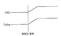
상기한 제어 방법의 경우, 배터리(BT)를 탑재하지 않는 전자기기에서는, 도 9에 도시된 바와 같이, 배터리(BT)를 충전하는 충전 전류(Ichg)가 0(제로)이다. 이 때문에, 충전 전류를 검출하는 에러 증폭기(14)의 출력 전류에 의해 제어 전류(Isc)의 전류값이 작아지고, 충전 회로는 최대의 출력 전압(Vout)을 출력한다. 그리고, 전자기기에 배터리를 장착하면, 배터리(BT)의 출력 전압보다도 높은 전압이 충전 회로로부터 출력되고 있기 때문에, 충전 전류(Ichg)가 크게 변화된다. 즉, 배터리(BT)에 대하여 큰 돌입 전류가 발생한다. 이 돌입 전류는 배터리(BT)의 허용 전류를 초과하기 때문에, 배터리(BT)가 열화할 우려가 있다.In the case of the control method described above, in the electronic device that does not mount the battery BT, as shown in FIG. 9, the charging current Ichg for charging the battery BT is 0 (zero). For this reason, the current value of the control current Isc becomes small by the output current of the
또한, 상기한 제어 방법의 경우, 배터리(BT)를 탑재한 전자기기에 교류 전원을 공급한 외부 전원을 접속하면, 그 접속했을 때에는 제어 전류(Isc)가 0(제로)이기 때문에, 충전 회로는 최대 전압을 출력하고, 상기와 마찬가지로 배터리(BT)에 대하여 큰 돌입 전류가 발생한다고 하는 문제가 있다.In addition, in the case of the control method described above, when an external power supply that supplies AC power to an electronic device equipped with a battery BT is connected, the control current Isc is 0 (zero) at that time. There is a problem that a maximum voltage is output and a large inrush current is generated for the battery BT as described above.
또한, 동작 전원 전압이 저하한 경우, 그것에 따른 충전 회로의 출력 전압이 저하하기 때문에, 낮은 동작 전원 전압에 의해 동작하는 충전 회로에 있어서 큰 제어 전류(Isc)를 흐르게 해야 한다. 이 때문에, 충전 회로가 동작적으로 전원 전압의 여유가 없어 충전 회로에 있어서 엄격한 동작 조건이 되어 버린다.In addition, when the operating power supply voltage decreases, the output voltage of the charging circuit corresponding thereto decreases, so that a large control current Isc must flow in the charging circuit operated by the low operating power supply voltage. For this reason, the charging circuit is operated and there is no margin of the power supply voltage, which results in strict operating conditions in the charging circuit.
본 발명은 상기 문제점을 해결하기 위해서 이루어진 것으로서, 그 목적은 외부 전원의 출력 전압의 제어가 가능하고, 돌입 전류를 억제할 수 있는 전원 시스템 및 출력 전압의 제어 방법을 제공하는 것에 있다.SUMMARY OF THE INVENTION The present invention has been made to solve the above problems, and an object thereof is to provide a power supply system and an output voltage control method capable of controlling an output voltage of an external power supply and suppressing an inrush current.
상기 목적을 달성하기 위해서 청구항 1에 기재한 발명은 직류의 출력 전압을 생성하는 외부 전원과, 상기 외부 전원의 출력 전압에 기초하여 동작하는 전자기기를 포함하는 전원 시스템에 있어서, 상기 외부 전원은 직류의 출력 전압을 생성하는 동시에 제어 전류에 따라 상기 출력 전압을 변경하는 전압 제어 회로를 구비하 고, 상기 전자기기는 2차 전지와, 상기 외부 전원의 출력 전압과 상기 2차 전지의 출력 전압 중 적어도 한쪽 전압에 기초하여 동작하는 시스템 회로와, 상기 2차 전지의 출력 전압과 상기 외부 전원의 출력 전류와 상기 2차 전지에 대한 충전 전류 중 적어도 하나와 검출 대상에 따른 기준 신호와의 차에 따라 상기 제어 전류를 발생시키는 검출 회로를 구비하며, 상기 전압 제어 회로는 상기 제어 전류가 최소인 경우에는 상기 출력 전압을 상기 외부 전원이 생성할 수 있는 최저 전압으로 제어하도록 하였다.In order to achieve the above object, the invention described in
검출 회로는 청구항 2에 기재한 발명과 같이, 상기 외부 전원의 출력 전력을 추가로 검출 대상으로 하여 상기 제어 전류를 생성하도록 하여도 좋다.As in the invention described in
이 구성에 따르면, 제어 전류가 공급되어 있지 않은 경우, 외부 전원은 최저 전압의 출력 전압을 생성한다. 따라서, 2차 전지를 탑재한 전자기기에 외부 전원을 접속하는 경우, 외부 전원의 출력 전압과 2차 전지의 전압과의 차가 적기 때문에, 큰 돌입 전류가 흐르는 것을 막을 수 있다. 또한, 전자기기에 2차 전지가 탑재되어 있지 않은 경우, 외부 전원은 최저 전압의 출력 전압을 전자기기에 공급한다. 이 때문에, 전자기기에 2차 전지를 장착한 경우, 2차 전지의 단자 전압과 외부 전원의 출력 전압과의 차가 적기 때문에, 2차 전지에 대한 돌입 전류가 억제된다.According to this configuration, when no control current is supplied, the external power supply produces the output voltage of the lowest voltage. Therefore, when the external power supply is connected to the electronic device equipped with the secondary battery, the difference between the output voltage of the external power supply and the voltage of the secondary battery is small, so that a large inrush current can be prevented from flowing. In addition, when the secondary battery is not mounted in the electronic device, the external power supply supplies the output voltage of the lowest voltage to the electronic device. For this reason, when the secondary battery is attached to the electronic device, the difference between the terminal voltage of the secondary battery and the output voltage of the external power supply is small, so that the inrush current to the secondary battery is suppressed.
청구항 3에 기재한 발명과 같이, 상기 검출 회로는 상기 검출 대상의 검출 결과와 상기 기준 신호와의 차에 따른 오차 전류를 발생시키는 증폭기와, 상기 증폭기에 의해 발생되는 오차 전류를 전압 변환하는 전류 전압 변환 회로와, 상기 전류 전압 변환 회로의 출력 전압이 공급되는 게이트와, 상기 출력 전압이 공급되는 제1 단자와, 단자를 통해 상기 외부 전원에 접속되는 제2 단자를 갖는 MOS 트랜지스터를 구비하고, 상기 전압 제어 회로는 상기 MOS 트랜지스터로부터 공급되는 제어 전류에 따라 상기 출력 전압을 제어한다.As in the invention described in claim 3, the detection circuit includes an amplifier for generating an error current according to a difference between the detection result of the detection target and the reference signal, and a current voltage for voltage conversion of the error current generated by the amplifier. A MOS transistor having a conversion circuit, a gate to which an output voltage of the current voltage conversion circuit is supplied, a first terminal to which the output voltage is supplied, and a second terminal to be connected to the external power source through a terminal; A voltage control circuit controls the output voltage in accordance with a control current supplied from the MOS transistor.
청구항 4에 기재한 발명과 같이, 상기 검출 회로는 상기 검출 대상의 검출 결과와 상기 기준 신호와의 차에 따른 오차 전류를 발생시키는 증폭기와, 상기 증폭기에 의해 발생되는 오차 전류를 전압 변환하는 전류 전압 변환 회로와, 상기 전류 전압 변환 회로의 출력 전압이 공급되는 게이트와, 그라운드에 접속된 제1 단자와, 단자를 통해 상기 외부 전원에 접속되는 제2 단자를 갖는 MOS 트랜지스터를 구비하고, 상기 전압 제어 회로는 상기 MOS 트랜지스터를 향해 흐르는 제어 전류에 따라 상기 출력 전압을 제어한다.As in the invention described in claim 4, the detection circuit includes an amplifier for generating an error current in accordance with a difference between the detection result of the detection target and the reference signal, and a current voltage for voltage conversion of the error current generated by the amplifier. A MOS transistor having a conversion circuit, a gate to which the output voltage of the current voltage conversion circuit is supplied, a first terminal connected to ground, and a second terminal connected to the external power supply via a terminal, wherein the voltage control The circuit controls the output voltage in accordance with a control current flowing toward the MOS transistor.
청구항 5에 기재한 발명은 외부 전원의 출력 전압을 전자기기에 공급하는 동시에 이 출력 전압을 상기 전자기기에 있어서 생성한 제어 전류에 따라 제어하는 출력 전압의 제어 방법으로서, 상기 전자기기는 상기 2차 전지의 출력 전압과 상기 외부 전원의 출력 전류와 2차 전지에 대한 충전 전류 중 적어도 하나와 검출 대상에 따른 기준 신호와의 차에 따라 상기 제어 전류를 발생시키고, 상기 외부 전원의 전압 제어 회로는 상기 제어 전류가 최소인 경우에는 상기 출력 전압을 상기 외부 전원이 생성할 수 있는 최저 전압으로 제어하도록 하였다.The invention as set forth in claim 5 is a control method of an output voltage which supplies an output voltage of an external power supply to an electronic device and simultaneously controls the output voltage according to a control current generated by the electronic device. The control current is generated according to a difference between at least one of an output voltage of a battery, an output current of the external power source and a charging current for a secondary battery, and a reference signal according to a detection target, and the voltage control circuit of the external power source When the control current is minimum, the output voltage is controlled to be the lowest voltage that the external power can generate.
상기 전자기기는 청구항 6에 기재한 발명과 같이, 상기 외부 전원의 출력 전력을 추가로 검출 대상으로 하여 상기 제어 전류를 생성하도록 하여도 좋다.As in the invention described in claim 6, the electronic device may further generate the control current by using the output power of the external power source as a detection target.
이 구성에 따르면, 제어 전류가 공급되어 있지 않은 경우, 외부 전원은 최저 전압의 출력 전압을 생성한다. 따라서, 2차 전지를 탑재한 전자기기에 외부 전원을 접속하는 경우, 외부 전원의 출력 전압과 2차 전지의 전압과의 차가 적기 때문에, 큰 돌입 전류가 흐르는 것을 막을 수 있다. 또한, 전자기기에 2차 전지가 탑재되어 있지 않은 경우, 외부 전원은 최저 전압의 출력 전압을 전자기기에 공급한다. 이 때문에, 전자기기에 2차 전지를 장착한 경우, 2차 전지의 단자 전압과 외부 전원의 출력 전압과의 차가 적기 때문에, 2차 전지에 대한 돌입 전류가 억제된다.According to this configuration, when no control current is supplied, the external power supply produces the output voltage of the lowest voltage. Therefore, when the external power supply is connected to the electronic device equipped with the secondary battery, the difference between the output voltage of the external power supply and the voltage of the secondary battery is small, so that a large inrush current can be prevented from flowing. In addition, when the secondary battery is not mounted in the electronic device, the external power supply supplies the output voltage of the lowest voltage to the electronic device. For this reason, when the secondary battery is attached to the electronic device, the difference between the terminal voltage of the secondary battery and the output voltage of the external power supply is small, so that the inrush current to the secondary battery is suppressed.
청구항 7에 기재한 발명과 같이, 상기 전자기기는 상기 검출 대상의 검출 결과와 상기 기준 신호와의 차에 따른 오차 전류를 발생시키는 증폭기와; 상기 증폭기에 의해 발생되는 오차 전류를 전압 변환하는 전류 전압 변환 회로와; 상기 전류 전압 변환 회로의 출력 전압이 공급되는 게이트와, 상기 출력 전압이 공급되는 제1 단자와, 단자를 통해 상기 외부 전원에 접속되는 제2 단자를 갖는 MOS 트랜지스터를 구비한 검출 회로를 가지며, 상기 외부 전원은 상기 MOS 트랜지스터로부터 공급되는 제어 전류에 따라 상기 출력 전압을 제어한다.As described in claim 7, the electronic device includes: an amplifier for generating an error current according to a difference between the detection result of the detection target and the reference signal; A current voltage conversion circuit for voltage converting the error current generated by the amplifier; A detection circuit having a MOS transistor having a gate to which an output voltage of the current voltage conversion circuit is supplied, a first terminal to which the output voltage is supplied, and a second terminal to be connected to the external power source through a terminal; An external power source controls the output voltage according to the control current supplied from the MOS transistor.
청구항 8에 기재한 발명과 같이, 상기 전자기기는 상기 검출 대상의 검출 결과와 상기 기준 신호와의 차에 따른 오차 전류를 발생시키는 증폭기와; 상기 증폭기에 의해 발생되는 오차 전류를 전압 변환하는 전류 전압 변환 회로와; 상기 전류 전압 변환 회로의 출력 전압이 공급되는 게이트와, 그라운드에 접속된 제1 단자와, 단자를 통해 상기 외부 전원에 접속되는 제2 단자를 갖는 MOS 트랜지스터를 구비한 검출 회로를 가지며, 상기 외부 전원은 상기 MOS 트랜지스터를 향해 흐르는 제어 전류에 따라 상기 출력 전압을 제어한다.As in the invention described in claim 8, the electronic device includes: an amplifier for generating an error current according to a difference between the detection result of the detection target and the reference signal; A current voltage conversion circuit for voltage converting the error current generated by the amplifier; A detection circuit having a MOS transistor having a gate to which an output voltage of the current voltage converting circuit is supplied, a first terminal connected to ground, and a second terminal connected to the external power supply through a terminal; Controls the output voltage according to a control current flowing toward the MOS transistor.
본 발명에 따르면, 외부 전원의 출력 전압의 제어가 가능하고, 돌입 전류를 억제할 수 있는 전원 시스템 및 출력 전압의 제어 방법을 제공할 수 있다.According to the present invention, it is possible to provide a power supply system capable of controlling the output voltage of an external power supply and suppressing an inrush current and a method of controlling the output voltage.
이하, 본 발명을 구체화한 일 실시 형태를 도 1 내지 도 4에 따라 설명한다.EMBODIMENT OF THE INVENTION Hereinafter, one Embodiment which actualized this invention is described according to FIGS.
도 1은 전원 시스템의 개략 구성도이다. 전원 시스템은 외부 전원으로서의 AC 어댑터(21)와, 그 AC 어댑터(21)에 접속된 전자기기(31)로 구성되어 있다. AC 어댑터(21)는 교류 전원(AC)에 접속되고, 이 교류 전원(AC)으로부터 공급되는 상용 교류 전압은 AC 어댑터(21)의 전압 변환 회로(22)에 입력된다. 전압 변환 회로(22)는 교류 전압을 교류-직류 변환하여 생성한 직류 전압을 출력한다. 전압 제어 회로(23)는 제어 전류(Isc)가 입력되고, 이 제어 전류(Isc)에 기초하여 직류 전압으로부터 제어한 어댑터 전압(VAC)을 생성한다. 이 어댑터 전압(VAC)은 전자기기(31)에 공급된다.1 is a schematic configuration diagram of a power supply system. The power supply system is composed of an
어댑터 전압(VAC)은 저항(R1)을 통해 시스템 DC/DC 컨버터(32)에 공급된다. 시스템 DC/DC 컨버터(32)에는 저항(R2)을 통해 2차 전지(배터리)(BT)가 접속되어 있다. 시스템 DC/DC 컨버터(32)는 어댑터 전압(VAC)과 배터리로부터 공급되는 배터리 전압에 기초하여 입력 전압을 전압 변환하여 생성한 시스템 전압(Vs)을 시스템 회로(33)에 공급한다. 따라서, 시스템 회로(33)에는 AC 어댑터(21)로부터 공급되는 전력과, 배터리(BT)로부터 공급되는 전력 중 적어도 한쪽에 의한 전력이 공급된다. 시스템 회로(33)는 전자기기(31)의 각종 기능을 제공하는 회로이다.The adapter voltage VAC is supplied to the system DC /
저항(R1) 및 저항(R2)은 배터리 검출 회로(34)에 접속되어 있다. 배터리 검출 회로(34)는 저항(R1)의 양 단자에 접속되는 동시에 저항(R2)과 배터리(BT) 사이에 접속되어 있다. 배터리 검출 회로(34)는 저항(R1)의 양 단자간의 전위차에 기초하여 이 저항(R1)에 흐르는 전류(Iout)를 검출한다. 또한, 배터리 검출 회로(34)는 저항(R2)의 양 단자간의 전위차에 기초하여 이 저항(R2)에 흐르는 전류(Ichg)를 검출한다. 또한, 배터리 검출 회로(34)는 시스템 DC/DC 컨버터(32)에 공급되는 전압[또는 어댑터 전압(VAC)]과 배터리(BT)의 단자 전압을 검출한다. 그리고, 배터리 검출 회로(34)는 검출한 전류, 전압에 기초하여 제어 전류(Isc)를 생성한다. 이 제어 전류(Isc)는 AC 어댑터(21)의 전압 제어 회로(23)에 공급된다. 따라서, AC 어댑터(21)의 전압 제어 회로(23)는 배터리 검출 회로(34)로부터 출력되는 제어 전류(Isc)에 따라 어댑터 전압(VAC)을 제어한다.The resistor R1 and the resistor R2 are connected to the
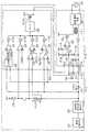
다음에, AC 어댑터(21)의 구성예를 설명한다. 도 2에 도시된 바와 같이, 전압 변환 회로(22)의 출력 단자는 제1 트랜지스터(T11)의 제1 단자(예컨대 소스)에 접속되고, 제1 트랜지스터(T11)의 제2 단자(예컨대 드레인)는 초크 코일(L1)의 제1 단자에 접속되며, 초크 코일(L1)의 제2 단자는 제1 단자(P1)에 접속되어 있다. 또한, 제1 트랜지스터(T11)의 제2 단자는 제2 트랜지스터(T12)의 제1 단자(예컨대 드레인)에 접속되고, 그 제2 트랜지스터(T12)의 제2 단자(예컨대 소스)는 그라운드에 접속되어 있다. 제1 트랜지스터(T11)의 제어 단자(게이트)와 제2 트랜지스터(T12)의 제어 단자(게이트)는 펄스폭 변조기(PWM)(24)에 접속되어 있다. 본 실시 형태에 있어서, 제1 트랜지스터(T11)는 P채널 MOS 트랜지스터이며, 제2 트랜지스터(T12)는 N 채널 MOS 트랜지스터이다. 또한, 도면에는 각 트랜지스터(T11, T12)의 보디 다이오드를 도시하고 있다.Next, a configuration example of the
상기 초크 코일(L1)의 제1 단자는 다이오드(D1)의 캐소드에 접속되고, 다이오드(D1)의 애노드는 그라운드에 접속되어 있다. 제1 단자(P1)는 평활용 콘덴서(C1)의 제1 단자에 접속되고, 콘덴서(C1)의 제2 단자는 그라운드에 접속되어 있다. 제2 단자(P2)는 그라운드에 접속되고, 제3 단자(P3)는 펄스폭 변조기(PWM)(24)에 접속되어 있다.The first terminal of the choke coil L1 is connected to the cathode of the diode D1, and the anode of the diode D1 is connected to ground. The first terminal P1 is connected to the first terminal of the smoothing capacitor C1, and the second terminal of the capacitor C1 is connected to ground. The second terminal P2 is connected to ground, and the third terminal P3 is connected to a pulse width modulator (PWM) 24.
펄스폭 변조기(24)에는 제3 단자(P3)를 통해 제어 전류(Isc)가 입력되어 있다. 펄스폭 변조기(PWM)(24)는 소정의 듀티 사이클로써 제1 트랜지스터(T11)와 제2 트랜지스터(T12)를 상보적으로 온/오프 제어한다. 제1 트랜지스터(T11)의 스위칭 동작에 의해 그 트랜지스터(T11)의 출력 전류는 초크 코일(L1) 및 콘덴서(C1)에 의해 평활된다. 여기서, 제1 트랜지스터(T11)가 온일 때에는 전압 변환 회로(22)의 출력 전압이 이 트랜지스터(T11)를 통해 LC 회로[초크 코일(L1)과 콘덴서(C1)로 이루어진 평활 회로]에 공급된다. 제1 트랜지스터(T11)가 오프되면, 다이오드(D1)를 통해 전류 경로가 형성된다. 이 때, 제1 트랜지스터(T11)가 온일 때에 초크 코일(L1)에 축적된 에너지가 제1 단자(P1)측으로 방출된다.The control current Isc is input to the
또한, 펄스폭 변조기(24)는 제어 전류(Isc)에 응답하여 듀티 사이클을 변경한다. 상세하게는, 펄스폭 변조기(24)는 제어 전류(Isc)의 전류값에 따라 제1 트랜지스터(T11)를 온하는 기간을 변화시키도록 듀티 사이클을 변경한다. AC 어댑터(21)로부터 출력되는 어댑터 전압(VAC)은 제1 트랜지스터(T11)의 온 기간에 대응 한다. 제1 트랜지스터(T11)의 온 기간이 길면, 초크 코일(L1)에 축적되는 에너지가 많아져 높은 어댑터 전압(VAC)이 출력되고, 제1 트랜지스터(T11)의 온 기간이 짧으면, 초크 코일(L1)에 축적되는 에너지가 적어져 낮은 어댑터 전압(VAC)이 출력된다.The
따라서, AC 어댑터(21)는 도 3에 도시된 바와 같이 제어 전류(Isc)에 따라 어댑터 전압(VAC)을 변경한다. 그리고, 제어 전류(Isc)가 공급되어 있지 않을 때, AC 어댑터(21)는 최저 전압의 어댑터 전압(VAC)을 출력한다. 이 때문에, 교류 전원(AC)에 접속한 AC 어댑터(21)를 전자기기(31)에 접속한 경우, 제어 전류(Isc)가 0(제로)이기 때문에, 최저 전압의 어댑터 전압(VAC)을 전자기기(31)에 공급한다. 이 때문에, 도 4에 도시된 바와 같이, 전자기기(31)에 탑재된 배터리(BT)에 대하여 큰 돌입 전류가 흐르는 것을 막을 수 있다.Therefore, the
다음에, 제어 전류(Isc)를 생성하는 구성, 즉, 전자기기(31)에 탑재된 배터리 검출 회로(34)의 구성을 설명한다.Next, the configuration for generating the control current Is, that is, the configuration of the
AC 어댑터(21)에 의해 생성된 어댑터 전압(VAC)은 전자기기(31)의 제1 단자(P11)를 통해 저항(R1)에 공급된다. 전자기기(31)의 저항(R1)에는 AC 어댑터(21)로부터 공급되는 전류(Iout)가 흐른다. 이 저항(R1)의 양 단자는 배터리 검출 회로(34)의 전류 증폭기(41)의 입력 단자에 접속되어 있다. 전류 증폭기(41)는 저항(R1)에 흐르는 전류(Iout), 즉 AC 어댑터(21)의 출력 전류를 검출하고, 그 검출 결과에 따른 전류 검출 신호(S1)를 에러 증폭기(42)에 출력한다. 에러 증폭기(42)는 반전 입력 단자에 전류 검출 신호(S1)가 입력되고, 비반전 입력 단자에 전류 기 준 신호(IOUTM)가 입력되어 있다. 전류 기준 신호(IOUTM)는 전자기기(31)에 있어서 사용되는 총 전류량에 따라 설정되어 있다. 에러 증폭기(42)는 전류 검출 신호(S1)와 전류 기준 신호(IOUTM)를 비교하고, 그 비교 결과에 따른 오차 전압을 발생한다.The adapter voltage VAC generated by the
배터리(BT)에 접속된 저항(R2)의 양 단자는 전류 증폭기(43)의 입력 단자에 접속되어 있다. 전류 증폭기(43)는 저항(R2)에 흐르는 전류(Ichg), 즉 배터리(BT) 에 대한 충전 전류(Ichg)를 검출하고, 그 전류량에 따른 충전 전류 검출 신호(S2)를 에러 증폭기(44)에 출력한다. 에러 증폭기(44)는 비반전 입력 단자에 배터리(BT)의 충전 전류에 따라 설정된 전압값의 제한 전류 신호(IDAC)가 입력되고, 반전 입력 단자에 충전 전류 검출 신호(S2)가 입력된다. 에러 증폭기(44)는 충전 전류 검출 신호(S2)의 전압과 제한 전류 신호(IDAC)의 전압과의 차를 증폭한 오차 전압을 발생한다.Both terminals of the resistor R2 connected to the battery BT are connected to the input terminal of the
저항(R2)과 배터리(BT) 사이의 접속점은 에러 증폭기(45)의 반전 입력 단자에 접속되어 있다. 그 에러 증폭기(45)의 비반전 입력 단자에는 전압 제한 신호(VDAC)가 입력된다. 에러 증폭기(45)는 배터리(BT)의 단자 전압과 전압 제한 신호(VDAC)와의 차를 증폭한 오차 전압을 발생한다.The connection point between the resistor R2 and the battery BT is connected to the inverting input terminal of the
상기 저항(R1)의 양 단자는 승산기(46)에 접속되어 있다. 승산기(46)는 저항(R1)의 단자 전압, 즉 어댑터 전압(VAC)을 검출하는 동시에 저항(R1)의 양 단자간 전압에 의해 총 전류량을 검출한다. 그리고, 승산기(46)는 어댑터 전압(VAC)과 총 전류량을 승산한 결과, 즉 총 전력량에 따른 전력 검출 신호(PWRO)를 에러 증폭 기(47)에 출력한다. 에러 증폭기(47)는 반전 입력 단자에 전력 검출 신호(PWRO)가 입력되고, 비반전 입력 단자에 전력 제한 신호(PWRM)가 입력된다. 에러 증폭기(47)는 전력 검출 신호(PWRO)와 전력 제한 신호(PWRM)의 차를 증폭한 오차 전압을 발생한다.Both terminals of the resistor R1 are connected to a
에러 증폭기(42, 44, 45, 47)의 출력 단자에는 다이오드(D11, D12, D13, D14)의 캐소드가 각각 접속되어 있다. 다이오드(D11∼D14)의 애노드는 공통 접속되는 동시에 전류 전압 변환 회로(48)에 접속되어 있다. 다이오드(D11∼D14)는 각 에러 증폭기(42, 44, 45, 47)의 출력 전압 중, 가장 큰 전압에 의존한 전류(오차 전류)를 전류 전압 변환 회로(48)에 전달한다. 이것은 각 검출값 중 가장 큰 에러(오차)의 검출값이다.The cathodes of the diodes D11, D12, D13, and D14 are connected to the output terminals of the
전류 전압 변환 회로(48)의 출력 단자에는 정전류원을 구성하는 트랜지스터(T21)의 제어 단자(게이트)가 접속되어 있다. 전류 전압 변환 회로(48)는 전류량에 비례한 전압값의 신호를 트랜지스터(T21)의 게이트에 공급한다. 이 트랜지스터(T21)는 본 실시 형태에서는 P 채널 MOS 트랜지스터로서, 소스에 어댑터 전압(VAC)이 공급되고, 드레인이 제3 단자(P13)에 접속되어 있다. 전자기기(31)의 제2 단자(P12)는 그라운드에 접속되어 있다.The control terminal (gate) of the transistor T21 constituting the constant current source is connected to the output terminal of the current
트랜지스터(T21)는 게이트에 공급되는 전압에 따른 저항체로서 동작하고, 그 저항값에 따른 제어 전류(Isc)를 흐르게 한다. 상기한 바와 같이, 트랜지스터(T21)는 P 채널 MOS 트랜지스터이기 때문에, 높은 게이트 전압에서는 저항값이 크고, 낮은 게이트 전압에서는 저항값이 작다. 따라서, 전류 전압 변환 회로(48)의 출력 전 압이 높은 경우, 즉, 검출 결과에 있어서 에러(오차)가 큰 경우, 트랜지스터(T21)는 적은 제어 전류(Isc)를 흐르게 하고, 전류 전압 변환 회로(48)의 출력 전압이 낮은 경우, 즉 검출 결과에 있어서 에러(오차)가 작은 경우, 트랜지스터(T21)는 큰 제어 전류(Isc)를 흐르게 하도록 동작한다.The transistor T21 operates as a resistor corresponding to the voltage supplied to the gate, and allows the control current Isc to flow according to the resistance value. As described above, since the transistor T21 is a P-channel MOS transistor, the resistance value is large at high gate voltage and small at low gate voltage. Therefore, when the output voltage of the current
배터리(BT)가 탑재되어 있지 않은 경우, 에러 증폭기(45)에 입력되는 단자 전압은 0(제로)이다. 또한, 에러 증폭기(44)에 의해 검출되는 충전 전류는 0이다. 따라서, 에러(오차)가 크고, 전류 전압 변환 회로(48)의 입력 전류가 크다. 이때, 트랜지스터(T21)는 적은 제어 전류(Isc)를 흐르게 하기 때문에, AC 어댑터(21)의 전압 제어 회로(23)는 낮은 어댑터 전압(VAC)을 출력한다. 이 상태에서 배터리(BT)를 장착한 경우, 배터리(BT)의 단자 전압과, AC 어댑터(21)로부터 공급되는 어댑터 전압(VAC)과의 차가 적어져 배터리(BT)에 대한 돌입 전류가 억제된다.When the battery BT is not mounted, the terminal voltage input to the
상기한 바와 같이 구성된 전원 시스템에 있어서, 동작 정지시 등과 같이 동작 전원 전압이 저하한 경우, 배터리 검출 회로(34)는 제어 전류(Isc)를 적게 하도록 동작하기 때문에, AC 어댑터(21)는 낮은 어댑터 전압(VAC)을 발생시킨다. 따라서, 배터리 검출 회로(34)에 있어서, 동작적으로 전원 전압에 여유가 생겨 동작 조건을 완화한다. 또한, AC 어댑터(21)는 낮은 어댑터 전압(VAC)을 공급하기 때문에, 낮은 입력 전압에 있어서 전자기기(31)가 동작을 정지하게 되고, 저전압시에 높은 어댑터 전압(VAC)이 공급되어 회로에 손상을 일으키는 것을 막을 수 있다.In the power supply system configured as described above, when the operating power supply voltage decreases, such as when the operation is stopped, the
이상 기술한 바와 같이, 본 실시 형태에 따르면, 이하가 효과를 발휘한다.As described above, according to the present embodiment, the following effects are obtained.
(1) AC 어댑터(21)는 제어 전류(Isc)에 따라 어댑터 전압(VAC)을 변경한다. 그리고, 제어 전류(Isc)가 공급되어 있지 않을 때, AC 어댑터(21)는 최저 전압의 어댑터 전압(VAC)을 출력한다. 이 때문에, 교류 전원(AC)에 접속한 AC 어댑터(21)를 전자기기(31)에 접속한 경우, 제어 전류(Isc)가 0(제로)이기 때문에, 최저 전압의 어댑터 전압(VAC)을 전자기기(31)에 공급한다. 이 때문에, 전자기기(31)에 탑재된 배터리(BT)에 대하여 큰 돌입 전류가 흐르는 것을 막을 수 있다.(1) The
(2) 배터리(BT)가 탑재되어 있지 않은 경우, 에러 증폭기(45)에 입력되는 단자 전압은 0(제로)이다. 또한, 에러 증폭기(44)에 의해 검출되는 충전 전류는 0이다. 따라서, 에러(오차)가 크고, 전류 전압 변환 회로(48)의 입력 전류가 크다. 이때, 트랜지스터(T21)는 적은 제어 전류(Isc)를 흐르게 하기 때문에, AC 어댑터(21)의 전압 제어 회로(23)는 낮은 어댑터 전압(VAC)을 출력한다. 이 상태에서, 배터리(BT)를 장착한 경우, 배터리(BT)의 단자 전압과, AC 어댑터(21)로부터 공급되는 어댑터 전압(VAC)과의 차가 적어져 배터리(BT)에 대한 돌입 전류를 억제할 수 있다.(2) When the battery BT is not mounted, the terminal voltage input to the
(3) 동작 정지시 등과 같이 동작 전원 전압이 저하한 경우, 배터리 검출 회로(34)는 제어 전류(Isc)를 적게 하도록 동작하기 때문에, AC 어댑터(21)는 낮은 어댑터 전압(VAC)을 발생시킨다. 따라서, 배터리 검출 회로(34)에 있어서, 동작적으로 전원 전압에 여유가 생겨 동작 조건을 완화한다. 또한, AC 어댑터(21)는 낮은 어댑터 전압(VAC)을 공급하기 때문에, 낮은 입력 전압에 있어서 전자기기(31)가 동작을 정지하게 되고, 저전압시에 높은 어댑터 전압(VAC)이 공급되어 회로에 손상을 일으키는 것을 막을 수 있다.(3) When the operating power supply voltage drops, such as when the operation stops, the
또한, 상기 실시 형태는 이하의 형태로 실시하여도 좋다.In addition, you may implement the said embodiment in the following aspects.
·상기 실시 형태에서는, 전자기기(31)의 배터리 검출 회로(34)로부터 AC 어댑터(21)에 제어 전류(Isc)를 공급하고, AC 어댑터(21)의 전압 제어 회로(23)는 제어 전류(Isc)가 제로인 경우에 어댑터 전압(VAC)을 최저 전압으로 하도록 하였지만, 배터리 검출 회로에 있어서, AC 어댑터로부터 제어 전류(Isc)를 유입시키도록 하여도 좋다. 예컨대, 도 5에 도시된 바와 같이, 배터리 검출 회로(34)는 제3 단자(P13)와 그라운드 사이에 접속된 트랜지스터(T21a)를 가지며, 이 트랜지스터(T21a)의 게이트는 전류 전압 변환 회로(48)에 접속되어 있다. 트랜지스터(T21a)는 N 채널 MOS 트랜지스터로서, 소스가 그라운드에 접속되고, 드레인이 제3 단자(P13)에 접속되어 있다. 따라서, 이 배터리 검출 회로(34)는 검출 대상에 있어서의 에러(오차)가 클 때에 AC 어댑터로부터 유입시키는 전류량을 적게 하고, 에러가 작을 때에 유입시키는 전류량을 많게 한다.In the above embodiment, the control current Isc is supplied to the
이 제어 전류(Isc)에 대하여, AC 어댑터는 제어 전류(Isc)가 0(제로)인 경우에 어댑터 전압(VAC)을 최저 전압으로 하고, 전자기기를 향해 흐르는 제어 전류(Isc)가 많아지면, 그 제어 전류(Isc)에 비례하여 어댑터 전압(VAC)을 높게 하도록 동작하면 좋다. 그 일례를 설명한다.With respect to this control current Isc, the AC adapter makes the adapter voltage VAC the lowest voltage when the control current Isc is 0 (zero), and when the control current Isc flowing toward the electronic device increases, The adapter voltage VAC may be increased in proportion to the control current Is. An example thereof will be described.
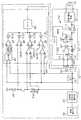
도 1에 도시된 전압 변환 회로(22)와 전압 제어 회로(23)는 도 5에 도시된 전압 변환 회로(25), 비교기(26), 트랜스(L11), 트랜지스터(T31), 기준 전원(e1), 저항(R11, R12) 및 콘덴서(C1)에 의해 구체화된다. 전압 변환 회로(25)의 입력 단자는 교류 전원(AC)에 접속되고, 전압 변환 회로(25)의 출력 단자는 트랜스(L11)의 입력측 코일에 접속되어 있다. 전압 변환 회로(25)는 교류 전원(AC)으로부터 공급되는 상용 교류 전압을 전압 변환하여 생성한 소정의 교류 전압을 트랜스(L11)의 입력측 코일에 발생시킨다.The
트랜스(L11)의 출력측 코일의 제1 단자는 제1 단자(P1)에 접속되고, 출력측 코일의 제2 단자는 트랜지스터(T31)에 접속되어 있다. 트랜지스터(T31)는 N 채널 MOS 트랜지스터로서, 소스가 그라운드에 접속되고, 드레인이 트랜스(L11)에 접속되며, 게이트가 비교기(26)의 출력 단자에 접속되어 있다.The first terminal of the output coil of the transformer L11 is connected to the first terminal P1, and the second terminal of the output coil is connected to the transistor T31. The transistor T31 is an N-channel MOS transistor with a source connected to ground, a drain connected to a transformer L11, and a gate connected to an output terminal of the
제1 단자(P1)에는 콘덴서(C1)의 제1 단자가 접속되고, 콘덴서(C1)의 제2 단자는 그라운드에 접속되며, 그 그라운드에는 제2 단자(P2)가 접속되어 있다. 또한, 제1 단자(P1)에는 저항(R11)의 제1 단자가 접속되고, 저항(R11)의 제2 단자는 저항(R12)의 제1 단자에 접속되며, 저항(R12)의 제2 단자는 그라운드에 접속되어 있다. 저항(R11)과 저항(R12) 사이의 접속점(노드)(N1)은 비교기(26)의 반전 입력 단자에 접속되고, 그 비교기(26)의 비반전 입력 단자는 기준 전원(e1)이 접속되어 있다. 또한, 비교기(26)의 반전 입력 단자, 즉 노드(N1)는 제3 단자(제어 단자)(P3)에 접속되어 있다.The first terminal of the capacitor C1 is connected to the first terminal P1, the second terminal of the capacitor C1 is connected to the ground, and the second terminal P2 is connected to the ground. In addition, a first terminal of the resistor R11 is connected to the first terminal P1, a second terminal of the resistor R11 is connected to a first terminal of the resistor R12, and a second terminal of the resistor R12 is connected. Is connected to ground. The connection point (node) N1 between the resistor R11 and the resistor R12 is connected to the inverting input terminal of the
AC 어댑터(21a)는 상기한 어댑터 전압(VAC)을 제1 단자(P1)로부터 출력한다. 그 제1 단자(P1)는 저항(R11, R12)을 통해 그라운드에 접속되어 있다. 따라서, 저항(R11, R12)은 각각의 저항값에 의해 노드(N1)에 어댑터 전압(VAC)을 분압한 분압 전압(Vn)을 발생시킨다. 또한, 노드(N1)는 제어 단자(P3)에 접속되고, 그 제어 단자(P3)로부터 제어 전류(Isc)가 입력된다. 이 제어 전류(Isc)는 저항(R12)에 흐르 는 전류량을 변화시키기 때문에, 노드(N1)에 발생하는 분압 전압(Vn)이 변경된다. 예컨대, 노드(N1)로부터 제어 단자(P3)를 향해 흐르는 제어 전류(Isc)가 감소되면, 저항(R12)을 흐르는 전류량이 증가하고, 노드(N1)의 전압(Vn)이 제어 전류(Isc)에 따른 전압만큼 상승한다. 한편, 노드(N1)로부터 제어 단자(P3)를 향해 흐르는 제어 전류(Isc)가 증가하면, 저항(R12)을 흐르는 전류량이 감소되고, 노드(N1)의 전압(Vn)이 제어 전류(Isc)에 따른 전압만큼 하강한다.The AC adapter 21a outputs the above-described adapter voltage VAC from the first terminal P1. The first terminal P1 is connected to ground via resistors R11 and R12. Accordingly, the resistors R11 and R12 generate the divided voltage Vn obtained by dividing the adapter voltage VAC at the node N1 by the respective resistance values. In addition, the node N1 is connected to the control terminal P3, and the control current Is is input from the control terminal P3. Since the control current Isc changes the amount of current flowing through the resistor R12, the divided voltage Vn generated at the node N1 is changed. For example, when the control current Isc flowing from the node N1 toward the control terminal P3 is decreased, the amount of current flowing through the resistor R12 increases, and the voltage Vn of the node N1 is the control current Isc. The voltage rises by. On the other hand, when the control current Isc flowing from the node N1 toward the control terminal P3 increases, the amount of current flowing through the resistor R12 is decreased, and the voltage Vn of the node N1 is the control current Isc. The voltage drops by.
비교기(26)는 노드(N1)의 전압(Vn)과 기준 전원(e1)에 의해 공급되는 기준 전압(Vr1)을 비교하고, 그 비교 결과에 따라 트랜지스터(T31)를 제어한다. 비교기(26)는 전압(Vn)이 기준 전압(Vr1)보다도 높은 경우에는 L 레벨의 신호를 트랜지스터(T31)의 게이트에 공급하고, 전압(Vn)이 기준 전압(Vr1)보다도 낮은 경우에는 H 레벨의 신호를 트랜지스터(T31)의 게이트에 공급한다. 트랜지스터(T31)는 L 레벨의 신호에 응답하여 오프되고, H 레벨의 신호에 응답하여 온된다. 트랜지스터(T31)가 온되면 트랜스(L11)의 출력측 코일에 교류 전류가 흐르고, 그 교류 전류가 콘덴서(C1)에 의해 평활화되어 어댑터 전압(VAC)이 생성된다. 그 어댑터 전압(VAC)을 분할한 전압(Vn)이 기준 전압(Vr1)보다도 높을 때에 트랜지스터(T31)가 오프되고, 전압(Vn)이 기준 전압(Vr1)보다도 낮을 때에 트랜지스터(T31)가 온된다. 따라서, 비교기(26)는 노드(N1)의 전압(Vn)이 기준 전압(Vr1)과 일치하도록 트랜지스터(T31)를 온/오프 제어한다.The
그 노드(N1)의 전압(Vn)은 제어 전류(Isc)에 의해 변경된다. 제어 전류(Isc)가 노드(N1)로부터 제3 단자(P3)를 향해 흐르면, 저항(R12)에 흐르는 전류가 적어 지고, 노드(N1)의 전압(Vn)이 낮아진다. 그렇게 하면, 비교기(26)는 노드(N1)의 전압(Vn)과 기준 전압(Vr1)을 일치시키도록 트랜지스터(T31)를 제어한다. 그 결과, 어댑터 전압(VAC)이 높아진다. 따라서, 제어 전류(Isc)가 흐르지 않는 경우, AC 어댑터(21a)는 어댑터 전압(VAC)을 최저 전압으로 한다.The voltage Vn of the node N1 is changed by the control current Isc. When the control current Isc flows from the node N1 toward the third terminal P3, the current flowing through the resistor R12 decreases, and the voltage Vn of the node N1 decreases. In doing so, the
·상기 각 실시 형태에 있어서, 도 2에 도시된 배터리 검출 회로(34)는 저항(R1)의 출력측 단자에 있어서의 전압(출력 전압)을 검출하도록 하였지만, 이것을 생략하여도 좋다. 즉, 승산기(46)와 에러 증폭기(47)와 다이오드(D14)를 생략한 배터리 검출 회로로 구체화하여도 좋다.In each of the above embodiments, the
·상기 각 실시 형태에서는, 제어 전류(Isc)에 대하여 어댑터 전압(VAC)을 비례적으로 제어하도록 하였지만, 제어 전류(Isc)와 어댑터 전압(VAC)과의 관계는 적절하게 변경되어도 좋다. 예컨대, 도 6(a)에 도시한 바와 같이, 제어 전류(Isc)의 증가에 따라 어댑터 전압(VAC)의 증가량을 적게 하여도 좋거나 또는 도 6(b)에 도시된 바와 같이, 제어 전류(Isc)의 증가에 따라 어댑터 전압(VAC)의 증가량을 많게 하도록 하여도 좋다. 또한, 도 6(c)에 도시된 바와 같이, 제어 전류(Isc)에 대하여 어댑터 전압(VAC)을 단계적으로 변경하도록 하여도 좋다. 또한, 도 6(d)에 도시된 바와 같이, 어댑터 전압(VAC)의 최저 전압을 0 V(제로 볼트)로 하도록 하여도 좋다. 또한, 음의 제어 전류(Isc)를 공급하도록 하여도 좋다. 또한, 도 6(e)에 도시된 바와 같이, 일정값 이상의 제어 전류(Isc)에 대하여 일정한 어댑터 전압(VAC)을 발생시키도록 하여도 좋다. 또한, 일정값 이하의 제어 전류(Isc)에 대하여 일정한 어댑터 전압(VAC)을 발생시키도록 하여도 좋다.In each of the above embodiments, the adapter voltage VAC is controlled to be proportionally controlled with respect to the control current Is, but the relationship between the control current Is and the adapter voltage VAC may be changed as appropriate. For example, as shown in FIG. 6 (a), the increase in the adapter voltage VAC may be reduced with increasing control current Is, or as shown in FIG. 6 (b), the control current ( The increase in the adapter voltage VAC may be increased with increasing Isc). In addition, as shown in FIG. 6C, the adapter voltage VAC may be changed in steps with respect to the control current Is. As shown in Fig. 6D, the lowest voltage of the adapter voltage VAC may be set to 0 V (zero volts). In addition, the negative control current Isc may be supplied. In addition, as shown in FIG. 6E, a constant adapter voltage VAC may be generated for a control current Isc of a predetermined value or more. In addition, a constant adapter voltage VAC may be generated for a control current Isc of a predetermined value or less.
·상기 각 실시 형태에서는, 제어 신호에 제어 전류를 이용하고 있었지만, 도 10에 도시된 바와 같이 전류 전압 변환 회로(48)의 출력 전압을 제어 신호로서 이용하여도 좋다.In each of the above embodiments, a control current is used for the control signal, but as shown in FIG. 10, the output voltage of the current
·상기 각 실시 형태에 있어서, AC 어댑터와 전자기기의 회로의 편성은 이들에 한정되지 않는다. 또한, AC 어댑터와 전자기기의 회로 구성은 상기 각 실시 형태에 한정되지 않는다.In each of the above embodiments, the combination of the circuit of the AC adapter and the electronic device is not limited to these. In addition, the circuit structure of an AC adapter and an electronic device is not limited to said each embodiment.
도 1은 일 실시 형태의 전원 시스템의 블록도.1 is a block diagram of a power supply system of one embodiment.
도 2는 일 실시 형태의 전원 시스템의 회로도.2 is a circuit diagram of a power supply system of one embodiment.
도 3은 일 실시 형태의 제어 전류와 어댑터 전압과의 특성도.3 is a characteristic diagram of control current and adapter voltage in one embodiment;
도 4는 일 실시 형태의 전원 시스템의 동작 파형도.4 is an operation waveform diagram of a power supply system of one embodiment;
도 5는 다른 전원 시스템의 회로도.5 is a circuit diagram of another power system.
도 6(a) 내지 도 6(e)은 다른 제어 전류와 어댑터 전압과의 특성도.6 (a) to 6 (e) are characteristic diagrams of other control currents and adapter voltages.
도 7은 종래의 전원 시스템의 회로도.7 is a circuit diagram of a conventional power supply system.
도 8은 종래의 제어 전류와 어댑터 전압과의 특성도.8 is a characteristic diagram of a conventional control current and an adapter voltage.
도 9는 종래의 전원 시스템의 동작 파형도.9 is an operational waveform diagram of a conventional power supply system.
도 10은 다른 전원 시스템의 회로도.10 is a circuit diagram of another power system.
〈도면의 주요 부분에 대한 부호의 설명〉<Explanation of symbols for main parts of drawing>
21 : AC 어댑터21: AC adapter
23 : 전압 제어 회로23: voltage control circuit
31 : 전자기기31: electronic device
33 : 시스템 회로33: system circuit
34 : 배터리 검출 회로34: battery detection circuit
48 : 전류 전압 변환 회로48: current voltage conversion circuit
BT : 2차 전지BT: Secondary Battery
Isc : 제어 전류Isc: control current
Ichg : 충전 전류Ichg: Charge Current
T21 : 트랜지스터T21: Transistor
VAC : 어댑터 전압VAC: Adapter Voltage
Claims (8)
Translated fromKoreanApplications Claiming Priority (2)
| Application Number | Priority Date | Filing Date | Title |
|---|---|---|---|
| JP2006251584AJP4984777B2 (en) | 2006-09-15 | 2006-09-15 | Power supply system and output voltage control method |
| JPJP-P-2006-00251584 | 2006-09-15 |
Publications (2)
| Publication Number | Publication Date |
|---|---|
| KR20080025322Atrue KR20080025322A (en) | 2008-03-20 |
| KR100963309B1 KR100963309B1 (en) | 2010-06-11 |
Family
ID=39188383
Family Applications (1)
| Application Number | Title | Priority Date | Filing Date |
|---|---|---|---|
| KR1020070093156AExpired - Fee RelatedKR100963309B1 (en) | 2006-09-15 | 2007-09-13 | Control method of power system and output voltage |
Country Status (5)
| Country | Link |
|---|---|
| US (1) | US7679343B2 (en) |
| JP (1) | JP4984777B2 (en) |
| KR (1) | KR100963309B1 (en) |
| CN (1) | CN101145699B (en) |
| TW (1) | TWI338832B (en) |
Cited By (1)
| Publication number | Priority date | Publication date | Assignee | Title |
|---|---|---|---|---|
| KR20170134731A (en)* | 2015-05-14 | 2017-12-06 | 로무 가부시키가이샤 | Power supply, AC adapter, AC charger, electronic equipment and power supply system |
Families Citing this family (15)
| Publication number | Priority date | Publication date | Assignee | Title |
|---|---|---|---|---|
| BRPI0700844A (en)* | 2007-03-20 | 2008-11-04 | Whirlpool Sa | electric motor driven compressor control system, electronic induction and control electric motor assembly, motor compressor arrangement and electric motor control method |
| JP2009178004A (en)* | 2008-01-28 | 2009-08-06 | Nec Electronics Corp | Power supply circuit |
| JP5332675B2 (en)* | 2008-03-31 | 2013-11-06 | 富士通セミコンダクター株式会社 | Electronic equipment and detection circuit |
| CN102013705A (en)* | 2009-09-08 | 2011-04-13 | 和硕联合科技股份有限公司 | Power supply system with power saving function and power supply method |
| US8810207B2 (en)* | 2010-11-17 | 2014-08-19 | Texas Instruments Incorporated | Communication systems and methods for transmitting communications between a charge system and an AC adapter |
| JP2012120267A (en) | 2010-11-29 | 2012-06-21 | Toshiba Corp | Charge controller |
| TWI454026B (en)* | 2011-05-24 | 2014-09-21 | Asustek Comp Inc | Power supply apparatus |
| JP5903993B2 (en)* | 2012-04-03 | 2016-04-13 | 住友電気工業株式会社 | Communications system |
| CN103779948A (en)* | 2012-10-23 | 2014-05-07 | 鸿富锦精密工业(深圳)有限公司 | Charging and discharging system and method |
| TWI513142B (en)* | 2013-04-26 | 2015-12-11 | 立錡科技股份有限公司 | Control method for supplying power |
| TWI540419B (en) | 2013-11-20 | 2016-07-01 | 鴻海精密工業股份有限公司 | Electronic device |
| CN104656724B (en)* | 2013-11-20 | 2016-05-25 | 鸿富锦精密工业(深圳)有限公司 | Electronic installation |
| TWI501064B (en)* | 2014-01-21 | 2015-09-21 | Celestica Technology Consultancy Shanghai Co Ltd | Hibrid power supply architecture |
| JP6520412B2 (en)* | 2015-06-01 | 2019-05-29 | 富士通クライアントコンピューティング株式会社 | Electronic device, power supply control device, and power supply system |
| CN109638917B (en)* | 2018-12-20 | 2023-10-13 | 上海艾为电子技术股份有限公司 | Charging circuit and electronic equipment |
Family Cites Families (10)
| Publication number | Priority date | Publication date | Assignee | Title |
|---|---|---|---|---|
| JP3368163B2 (en)* | 1996-12-18 | 2003-01-20 | インターナショナル・ビジネス・マシーンズ・コーポレーション | Power supply for electronic equipment and electronic equipment |
| JP3735999B2 (en) | 1997-02-20 | 2006-01-18 | ソニー株式会社 | Charger |
| JP4195959B2 (en)* | 1998-08-07 | 2008-12-17 | パナソニック株式会社 | Uninterruptible power system |
| JP3895496B2 (en)* | 1999-04-09 | 2007-03-22 | 富士通株式会社 | Charging control circuit, charging device, and charging control method |
| JP3428955B2 (en) | 2000-08-25 | 2003-07-22 | オーツー・マイクロ・インターナショナル・リミテッド | Buffer battery power supply system |
| TW521468B (en)* | 2001-06-14 | 2003-02-21 | Quanta Comp Inc | Charging apparatus capable of dynamically adjusting charging power |
| US6628107B1 (en)* | 2001-10-31 | 2003-09-30 | Symbol Technologies, Inc. | Power management for a portable electronic device |
| US7034413B1 (en)* | 2002-08-12 | 2006-04-25 | Network Appliance, Inc. | Holdup time extender and inrush current eliminator for switching power supplies |
| JP2006230073A (en)* | 2005-02-16 | 2006-08-31 | Canon Inc | Power supply |
| TWI299228B (en)* | 2005-05-18 | 2008-07-21 | Ite Tech Inc | Power supply conversion circuit and method thereof, and a circuitry incorporating the same |
- 2006
- 2006-09-15JPJP2006251584Apatent/JP4984777B2/ennot_activeExpired - Fee Related
- 2007
- 2007-09-07TWTW096133470Apatent/TWI338832B/ennot_activeIP Right Cessation
- 2007-09-13USUS11/898,575patent/US7679343B2/ennot_activeExpired - Fee Related
- 2007-09-13KRKR1020070093156Apatent/KR100963309B1/ennot_activeExpired - Fee Related
- 2007-09-14CNCN2007101521805Apatent/CN101145699B/ennot_activeExpired - Fee Related
Cited By (2)
| Publication number | Priority date | Publication date | Assignee | Title |
|---|---|---|---|---|
| KR20170134731A (en)* | 2015-05-14 | 2017-12-06 | 로무 가부시키가이샤 | Power supply, AC adapter, AC charger, electronic equipment and power supply system |
| US10333409B2 (en) | 2015-05-14 | 2019-06-25 | Rohm Co., Ltd. | Power delivery device, AC adapter, AC charger, electronic apparatus and power delivery system |
Also Published As
| Publication number | Publication date |
|---|---|
| TW200828004A (en) | 2008-07-01 |
| CN101145699B (en) | 2011-01-12 |
| US20080068871A1 (en) | 2008-03-20 |
| US7679343B2 (en) | 2010-03-16 |
| JP4984777B2 (en) | 2012-07-25 |
| JP2008072877A (en) | 2008-03-27 |
| CN101145699A (en) | 2008-03-19 |
| KR100963309B1 (en) | 2010-06-11 |
| TWI338832B (en) | 2011-03-11 |
Similar Documents
| Publication | Publication Date | Title |
|---|---|---|
| KR100963309B1 (en) | Control method of power system and output voltage | |
| US8829864B2 (en) | Current driver circuit | |
| KR100744592B1 (en) | Dc-dc converter, dc-dc converter control circuit, and dc-dc converter control method | |
| CN202798467U (en) | DC/DC converter, power supply device applying DC/DC converter, and electronic device | |
| EP3282571B1 (en) | Power converter with extended hold-up time | |
| US6661684B2 (en) | AC-to-DC converter | |
| CN105515418A (en) | PFC shutdown circuit for light load | |
| KR101086104B1 (en) | Detection circuit and power system | |
| JP4963068B2 (en) | Power factor correction circuit | |
| JP2010088150A (en) | Charger | |
| JP2001078370A (en) | Charger and charging control circuit | |
| KR20080076730A (en) | Detection circuit and power system | |
| JP2009247101A (en) | Charger device | |
| US9837845B2 (en) | Charging controlling circuit and charging controlling system | |
| US20120268090A1 (en) | Switching power supply device | |
| CN118539758A (en) | Charging control for resonant converters | |
| JP2010172154A (en) | Power supply control circuit, power supply control method, and electronic device | |
| US20120182000A1 (en) | Soft start circuit | |
| JP5332675B2 (en) | Electronic equipment and detection circuit | |
| CN113489296A (en) | Active compensation control circuit and method | |
| JP2020120514A (en) | Voltage conversion device | |
| US8890485B2 (en) | Charger circuit | |
| JP2006325330A (en) | Power system | |
| HK1157946B (en) | Circuit and method for determining a current | |
| HK1157946A1 (en) | Circuit and method for determining a current |
Legal Events
| Date | Code | Title | Description |
|---|---|---|---|
| A201 | Request for examination | ||
| PA0109 | Patent application | St.27 status event code:A-0-1-A10-A12-nap-PA0109 | |
| PA0201 | Request for examination | St.27 status event code:A-1-2-D10-D11-exm-PA0201 | |
| PG1501 | Laying open of application | St.27 status event code:A-1-1-Q10-Q12-nap-PG1501 | |
| N231 | Notification of change of applicant | ||
| PN2301 | Change of applicant | St.27 status event code:A-3-3-R10-R13-asn-PN2301 St.27 status event code:A-3-3-R10-R11-asn-PN2301 | |
| P11-X000 | Amendment of application requested | St.27 status event code:A-2-2-P10-P11-nap-X000 | |
| P13-X000 | Application amended | St.27 status event code:A-2-2-P10-P13-nap-X000 | |
| D13-X000 | Search requested | St.27 status event code:A-1-2-D10-D13-srh-X000 | |
| D14-X000 | Search report completed | St.27 status event code:A-1-2-D10-D14-srh-X000 | |
| E902 | Notification of reason for refusal | ||
| PE0902 | Notice of grounds for rejection | St.27 status event code:A-1-2-D10-D21-exm-PE0902 | |
| R18-X000 | Changes to party contact information recorded | St.27 status event code:A-3-3-R10-R18-oth-X000 | |
| E701 | Decision to grant or registration of patent right | ||
| PE0701 | Decision of registration | St.27 status event code:A-1-2-D10-D22-exm-PE0701 | |
| PN2301 | Change of applicant | St.27 status event code:A-3-3-R10-R13-asn-PN2301 St.27 status event code:A-3-3-R10-R11-asn-PN2301 | |
| GRNT | Written decision to grant | ||
| PR0701 | Registration of establishment | St.27 status event code:A-2-4-F10-F11-exm-PR0701 | |
| PR1002 | Payment of registration fee | St.27 status event code:A-2-2-U10-U11-oth-PR1002 Fee payment year number:1 | |
| PG1601 | Publication of registration | St.27 status event code:A-4-4-Q10-Q13-nap-PG1601 | |
| FPAY | Annual fee payment | Payment date:20130524 Year of fee payment:4 | |
| PR1001 | Payment of annual fee | St.27 status event code:A-4-4-U10-U11-oth-PR1001 Fee payment year number:4 | |
| PN2301 | Change of applicant | St.27 status event code:A-5-5-R10-R11-asn-PN2301 | |
| PN2301 | Change of applicant | St.27 status event code:A-5-5-R10-R14-asn-PN2301 | |
| FPAY | Annual fee payment | Payment date:20140526 Year of fee payment:5 | |
| PR1001 | Payment of annual fee | St.27 status event code:A-4-4-U10-U11-oth-PR1001 Fee payment year number:5 | |
| R18-X000 | Changes to party contact information recorded | St.27 status event code:A-5-5-R10-R18-oth-X000 | |
| FPAY | Annual fee payment | Payment date:20151023 Year of fee payment:6 | |
| PR1001 | Payment of annual fee | St.27 status event code:A-4-4-U10-U11-oth-PR1001 Fee payment year number:6 | |
| LAPS | Lapse due to unpaid annual fee | ||
| PC1903 | Unpaid annual fee | St.27 status event code:A-4-4-U10-U13-oth-PC1903 Not in force date:20160605 Payment event data comment text:Termination Category : DEFAULT_OF_REGISTRATION_FEE | |
| R18-X000 | Changes to party contact information recorded | St.27 status event code:A-5-5-R10-R18-oth-X000 | |
| PC1903 | Unpaid annual fee | St.27 status event code:N-4-6-H10-H13-oth-PC1903 Ip right cessation event data comment text:Termination Category : DEFAULT_OF_REGISTRATION_FEE Not in force date:20160605 |