KR20080023907A - Electrophoretic display device and manufacturing method thereof - Google Patents
Electrophoretic display device and manufacturing method thereofDownload PDFInfo
- Publication number
- KR20080023907A KR20080023907AKR1020060088033AKR20060088033AKR20080023907AKR 20080023907 AKR20080023907 AKR 20080023907AKR 1020060088033 AKR1020060088033 AKR 1020060088033AKR 20060088033 AKR20060088033 AKR 20060088033AKR 20080023907 AKR20080023907 AKR 20080023907A
- Authority
- KR
- South Korea
- Prior art keywords
- electrophoretic
- electrode
- transfer
- transfer film
- display panel
- Prior art date
- Legal status (The legal status is an assumption and is not a legal conclusion. Google has not performed a legal analysis and makes no representation as to the accuracy of the status listed.)
- Withdrawn
Links
Images


Classifications
- G—PHYSICS
- G02—OPTICS
- G02F—OPTICAL DEVICES OR ARRANGEMENTS FOR THE CONTROL OF LIGHT BY MODIFICATION OF THE OPTICAL PROPERTIES OF THE MEDIA OF THE ELEMENTS INVOLVED THEREIN; NON-LINEAR OPTICS; FREQUENCY-CHANGING OF LIGHT; OPTICAL LOGIC ELEMENTS; OPTICAL ANALOGUE/DIGITAL CONVERTERS
- G02F1/00—Devices or arrangements for the control of the intensity, colour, phase, polarisation or direction of light arriving from an independent light source, e.g. switching, gating or modulating; Non-linear optics
- G02F1/01—Devices or arrangements for the control of the intensity, colour, phase, polarisation or direction of light arriving from an independent light source, e.g. switching, gating or modulating; Non-linear optics for the control of the intensity, phase, polarisation or colour
- G02F1/165—Devices or arrangements for the control of the intensity, colour, phase, polarisation or direction of light arriving from an independent light source, e.g. switching, gating or modulating; Non-linear optics for the control of the intensity, phase, polarisation or colour based on translational movement of particles in a fluid under the influence of an applied field
- G02F1/1675—Constructional details
- G02F1/1679—Gaskets; Spacers; Sealing of cells; Filling or closing of cells
- G—PHYSICS
- G02—OPTICS
- G02F—OPTICAL DEVICES OR ARRANGEMENTS FOR THE CONTROL OF LIGHT BY MODIFICATION OF THE OPTICAL PROPERTIES OF THE MEDIA OF THE ELEMENTS INVOLVED THEREIN; NON-LINEAR OPTICS; FREQUENCY-CHANGING OF LIGHT; OPTICAL LOGIC ELEMENTS; OPTICAL ANALOGUE/DIGITAL CONVERTERS
- G02F1/00—Devices or arrangements for the control of the intensity, colour, phase, polarisation or direction of light arriving from an independent light source, e.g. switching, gating or modulating; Non-linear optics
- G02F1/01—Devices or arrangements for the control of the intensity, colour, phase, polarisation or direction of light arriving from an independent light source, e.g. switching, gating or modulating; Non-linear optics for the control of the intensity, phase, polarisation or colour
- G02F1/165—Devices or arrangements for the control of the intensity, colour, phase, polarisation or direction of light arriving from an independent light source, e.g. switching, gating or modulating; Non-linear optics for the control of the intensity, phase, polarisation or colour based on translational movement of particles in a fluid under the influence of an applied field
- G02F1/166—Devices or arrangements for the control of the intensity, colour, phase, polarisation or direction of light arriving from an independent light source, e.g. switching, gating or modulating; Non-linear optics for the control of the intensity, phase, polarisation or colour based on translational movement of particles in a fluid under the influence of an applied field characterised by the electro-optical or magneto-optical effect
- G02F1/167—Devices or arrangements for the control of the intensity, colour, phase, polarisation or direction of light arriving from an independent light source, e.g. switching, gating or modulating; Non-linear optics for the control of the intensity, phase, polarisation or colour based on translational movement of particles in a fluid under the influence of an applied field characterised by the electro-optical or magneto-optical effect by electrophoresis
- G—PHYSICS
- G02—OPTICS
- G02F—OPTICAL DEVICES OR ARRANGEMENTS FOR THE CONTROL OF LIGHT BY MODIFICATION OF THE OPTICAL PROPERTIES OF THE MEDIA OF THE ELEMENTS INVOLVED THEREIN; NON-LINEAR OPTICS; FREQUENCY-CHANGING OF LIGHT; OPTICAL LOGIC ELEMENTS; OPTICAL ANALOGUE/DIGITAL CONVERTERS
- G02F1/00—Devices or arrangements for the control of the intensity, colour, phase, polarisation or direction of light arriving from an independent light source, e.g. switching, gating or modulating; Non-linear optics
- G02F1/01—Devices or arrangements for the control of the intensity, colour, phase, polarisation or direction of light arriving from an independent light source, e.g. switching, gating or modulating; Non-linear optics for the control of the intensity, phase, polarisation or colour
- G02F1/165—Devices or arrangements for the control of the intensity, colour, phase, polarisation or direction of light arriving from an independent light source, e.g. switching, gating or modulating; Non-linear optics for the control of the intensity, phase, polarisation or colour based on translational movement of particles in a fluid under the influence of an applied field
- G02F1/1675—Constructional details
- G02F1/16757—Microcapsules
- G—PHYSICS
- G02—OPTICS
- G02F—OPTICAL DEVICES OR ARRANGEMENTS FOR THE CONTROL OF LIGHT BY MODIFICATION OF THE OPTICAL PROPERTIES OF THE MEDIA OF THE ELEMENTS INVOLVED THEREIN; NON-LINEAR OPTICS; FREQUENCY-CHANGING OF LIGHT; OPTICAL LOGIC ELEMENTS; OPTICAL ANALOGUE/DIGITAL CONVERTERS
- G02F1/00—Devices or arrangements for the control of the intensity, colour, phase, polarisation or direction of light arriving from an independent light source, e.g. switching, gating or modulating; Non-linear optics
- G02F1/01—Devices or arrangements for the control of the intensity, colour, phase, polarisation or direction of light arriving from an independent light source, e.g. switching, gating or modulating; Non-linear optics for the control of the intensity, phase, polarisation or colour
- G02F1/13—Devices or arrangements for the control of the intensity, colour, phase, polarisation or direction of light arriving from an independent light source, e.g. switching, gating or modulating; Non-linear optics for the control of the intensity, phase, polarisation or colour based on liquid crystals, e.g. single liquid crystal display cells
- G02F1/133—Constructional arrangements; Operation of liquid crystal cells; Circuit arrangements
- G02F1/1333—Constructional arrangements; Manufacturing methods
- G02F1/1341—Filling or closing of cells
- G—PHYSICS
- G02—OPTICS
- G02F—OPTICAL DEVICES OR ARRANGEMENTS FOR THE CONTROL OF LIGHT BY MODIFICATION OF THE OPTICAL PROPERTIES OF THE MEDIA OF THE ELEMENTS INVOLVED THEREIN; NON-LINEAR OPTICS; FREQUENCY-CHANGING OF LIGHT; OPTICAL LOGIC ELEMENTS; OPTICAL ANALOGUE/DIGITAL CONVERTERS
- G02F2203/00—Function characteristic
- G02F2203/34—Colour display without the use of colour mosaic filters
Landscapes
- Physics & Mathematics (AREA)
- Nonlinear Science (AREA)
- General Physics & Mathematics (AREA)
- Optics & Photonics (AREA)
- Health & Medical Sciences (AREA)
- Life Sciences & Earth Sciences (AREA)
- Chemical & Material Sciences (AREA)
- Chemical Kinetics & Catalysis (AREA)
- Electrochemistry (AREA)
- Molecular Biology (AREA)
- Electrochromic Elements, Electrophoresis, Or Variable Reflection Or Absorption Elements (AREA)
Abstract
Translated fromKoreanDescription
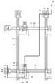
Translated fromKorean도 1은 본 발명의 한 실시예에 따른 전기 영동 표시 장치의 구조를 도시한 배치도이고,1 is a layout view illustrating a structure of an electrophoretic display device according to an exemplary embodiment of the present invention.
도 2는 도1의 전기 영동 표시 소자를 II-II' 선에 따라 자른 단면도이고,FIG. 2 is a cross-sectional view of the electrophoretic display device of FIG. 1 taken along line II-II ',
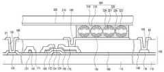
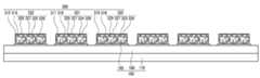
도 3은 본 발명의 한 실시예에 따른 전기 영동 표시 장치의 3개의 화소 영역을 도시한 단면도,3 is a cross-sectional view illustrating three pixel areas of an electrophoretic display device according to an exemplary embodiment of the present invention;
도 4a 내지 도 4i는 본 발명의 한 실시예에 따른 전기 영동 표시 장치의 제조 방법을 순차적으로 도시한 단면도이고,4A to 4I are cross-sectional views sequentially illustrating a method of manufacturing an electrophoretic display device according to an exemplary embodiment of the present invention.
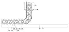
도 5는 본 발명의 한 실시예에 따른 전기 영동 표시 장치의 다른 제조 방법을 나타낸 단면도이고,5 is a cross-sectional view illustrating another manufacturing method of an electrophoretic display device according to an exemplary embodiment of the present invention.
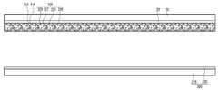
도 6은 본 발명의 다른 실시예에 따른 전기 영동 표시 장치의 3개의 화소 영역을 도시한 단면도이고,6 is a cross-sectional view illustrating three pixel areas of an electrophoretic display device according to another exemplary embodiment of the present invention.
도 7 및 도 8은 본 발명의 다른 실시예에 따른 전기 영동 표시 장치의 제조 방법을 순차적으로 도시한 단면도이다.7 and 8 are cross-sectional views sequentially illustrating a method of manufacturing an electrophoretic display device according to another exemplary embodiment of the present invention.
<도면의 주요 부분에 대한 부호의 설명><Explanation of symbols for the main parts of the drawings>
10, 11, 12, 13: 전사용 기판 20: 열 변환막10, 11, 12, 13: Transfer substrate 20: Heat conversion film
30: 도포 부재 100: 박막트랜지스터 표시판30: coating member 100: thin film transistor display panel
110: 절연 기판 121: 게이트선110: insulating substrate 121: gate line
124: 게이트 전극 129: 게이트선의 끝부분124: gate electrode 129: end of gate line
140: 게이트 절연막 151: 선형 반도체층140: gate insulating film 151: linear semiconductor layer
161: 선형 저항성 접촉 부재 171: 데이터선161: linear ohmic contact 171: data line
173: 소스 전극 175: 드레인 전극173: source electrode 175: drain electrode
179: 데이터선의 끝부분 180: 보호막179: end of the data line 180: protective film
181, 182, 185: 접촉구 190: 화소 전극181, 182, and 185: contact hole 190: pixel electrode
200: 공통 전극 표시판 210: 절연 기판200: common electrode display panel 210: insulating substrate
220: 공통 전극 301, 301: 전기 영동부220:
310, 311, 312, 313: 전사 필름 315: 전사 필름 형성 물질310, 311, 312, and 313: transfer film 315: transfer film forming material
316: 자외선 경화제 320, 321, 322, 330: 전기 영동 부재316:
323, 324, 325, 326, 328: 전기 영동 입자323, 324, 325, 326, 328: electrophoretic particles
327: 분산매 329: 캡슐327: dispersion medium 329: capsule
본 발명은 전기 영동 표시 장치 및 그 제조 방법에 관한 것이다.The present invention relates to an electrophoretic display device and a manufacturing method thereof.
최근 기존의 브라운관을 대체하여 액정표시장치, 유기 전계 발광 장치(OLED) 및 전기 영동 표시 장치(ELECTROPHORETIC DISPLAY) 등의 평판(flat panel)형 표시 장치가 많이 사용되고 있다.Recently, flat panel displays such as liquid crystal displays, organic light emitting diodes (OLEDs), and electrophoretic displays (ELECTROPHORETIC DISPLAYs) have been used in place of existing CRTs.
이 중 전기 영동 표시 장치는 화소 전극 및 공통 전극에 인가된 전압에 따라 양 또는 음의 전하를 띠며 소정의 색상을 갖는 전기 영동 입자가 회전하거나, 화소 전극 또는 공통 전극 가까이로 이동하는 방식으로 원하는 색상을 표현한다.Among these, the electrophoretic display device has a desired color in such a manner that electrophoretic particles having a predetermined color rotate or move near the pixel electrode or the common electrode, having a positive or negative charge depending on the voltage applied to the pixel electrode and the common electrode. Express
이러한 전기 영동 표시 장치의 제조 과정을 살펴보면 먼저 전기 영동 입자 및 전기 영동 입자가 분산된 분산매를 가두고 있는 마이크로 캡슐(microcapsule)을 포함하는 전기 영동 부재를 마련한다. 그런 다음 제1 표시판의 화소 전극 또는 화소 전극에 대응하는 제2 표시판의 공통 전극 중 어느 하나에 바인더(binder)를 도포하고 도포된 바인더에 전기 영동 부재를 배치시키거나, 전기 영동 부재가 분산되어 있는 바인더를 도포한다. 그런 다음 바인더를 경화하면 전기 영동 부재가 화소 전극 또는 공통 전극에 부착 고정된다. 이 후 부착 고정된 전기 영동 부재 위에 부착되지 않은 공통 전극 또는 화소 전극이 위치하도록 제2 표시판 또는 제1 표시판을 밀착하는 공정을 거친다.Referring to the manufacturing process of the electrophoretic display device, an electrophoretic member including a microcapsule containing an electrophoretic particle and a dispersion medium in which the electrophoretic particle is dispersed is prepared. Then, a binder is applied to either the pixel electrode of the first display panel or the common electrode of the second display panel corresponding to the pixel electrode, and the electrophoretic member is disposed on the applied binder, or the electrophoretic member is dispersed. Apply the binder. Then, when the binder is cured, the electrophoretic member is attached and fixed to the pixel electrode or the common electrode. Thereafter, the second display panel or the first display panel may be in close contact with each other so that the common electrode or the pixel electrode, which is not attached, is positioned on the attached and fixed electrophoretic member.
그러나 바인더를 이용하여 전기 영동 부재를 화소 전극 또는 공통 전극에 부착하는 공정은 복잡하며, 화소 전극 또는 공통 전극의 원하는 부분에 정확하게 바인더를 도포하고 전기 영동 부재를 부착하는 것이 용이하지 않아 전기 영동 표시 장치의 제조 효율이 떨어지고 제조된 전기 영동 표시 장치의 표시 성능이 저하되는 문제점이 있다.However, the process of attaching the electrophoretic member to the pixel electrode or the common electrode using a binder is complicated, and it is not easy to apply the binder to the desired portion of the pixel electrode or the common electrode accurately and attach the electrophoretic member to the electrophoretic display device. There is a problem that the manufacturing efficiency of the degradation and the display performance of the manufactured electrophoretic display device is lowered.
따라서, 본 발명이 이루고자 하는 기술적 과제는 이러한 문제점을 해결하여 제조 효율과 표시 성능이 우수한 전기 영동 표시 장치 및 그 제조 방법을 제공하는데 있다. Accordingly, an object of the present invention is to solve the above problems and to provide an electrophoretic display device having excellent manufacturing efficiency and display performance and a method of manufacturing the same.
본 발명에 따른 전기 영동 표시 장치는 제1 전극을 포함하는 제1 표시판, 상기 제1 전극과 마주하는 제2 전극을 포함하는 제2 표시판, 그리고 상기 제1 전극과 상기 제2 전극 사이에 위치하며, 상기 제1 전극 또는 상기 제2 전극에 레이저 열 전사(laser induced thermal imaging; LITI)법에 의해 부착되어 있으며, 전기 영동 부재와 상기 전기 영동 부재를 분산 고정하는 전사 필름을 포함하는 전기 영동부를 포함한다.An electrophoretic display device according to the present invention includes a first display panel including a first electrode, a second display panel including a second electrode facing the first electrode, and positioned between the first electrode and the second electrode. And an electrophoretic part attached to the first electrode or the second electrode by a laser induced thermal imaging (LITI) method, the electrophoretic part including an electrophoretic member and a transfer film dispersing and fixing the electrophoretic member. do.
상기 전기 영동 부재는, 흰색을 갖는 제1 전기 영동 입자, 검은색을 갖는 제2 전기 영동 입자, 상기 제1 및 제2 전기 영동 입자가 분산되어 있는 분산매, 그리고 상기 제1 및 제2 전기 영동 입자 및 상기 분산매를 가두고 있는 캡슐을 포함할 수 있다.The electrophoretic member may include a first electrophoretic particle having white color, a second electrophoretic particle having black color, a dispersion medium in which the first and second electrophoretic particles are dispersed, and the first and second electrophoretic particle And it may include a capsule containing the dispersion medium.
상기 전기 영동 부재는, 적색, 녹색 및 청색 중 어느 하나의 색을 갖거나 노란색, 마젠타(magenta), 시안(cyan) 중 어느 하나의 색을 갖는 전기 영동 입자, 상기 전기 영동 입자가 분산되어 있는 분산매, 그리고 상기 전기 영동 입자 및 상기 분산매를 가두고 있는 캡슐을 포함할 수 있다.The electrophoretic member may include electrophoretic particles having any one of red, green, and blue colors, or any one of yellow, magenta, and cyan, and a dispersion medium in which the electrophoretic particles are dispersed. And it may include a capsule containing the electrophoretic particles and the dispersion medium.
상기 전기 영동 부재는, 상기 분산매에 분산되어 있으며 검은색을 갖는 추가의 전기 영동 입자를 더 포함할 수 있다.The electrophoretic member may further include additional electrophoretic particles dispersed in the dispersion medium and having a black color.
상기 전사 필름은 자외선 경화제가 포함된 유기 필름일 수 있다.The transfer film may be an organic film including an ultraviolet curing agent.
상기 제1 전극은 공통 전극이며, 상기 제2 전극은 화소 전극일 수 있다.The first electrode may be a common electrode, and the second electrode may be a pixel electrode.
또한, 본 발명에 따른 전기 영동 표시 장치의 제조 방법은 전사용 기판 위에 열 변환막을 형성하는 단계, 상기 열 변환막 위에 전기 영동 부재가 분산되어 있는 전사 필름을 형성하는 단계, 제1 전극이 형성되어 있는 제1 표시판을 마련하여 상기 제1 표시판과 상기 전사용 기판을 정렬하는 단계, 레이저 열 전사(laser induced thermal imaging; LITI)법에 의해 상기 전사 필름의 소정 부분을 상기 제1 전극 위로 전사하는 단계, 그리고 제2 전극이 형성되어 있는 제2 표시판을 마련하여 상기 제2 전극과 전사된 상기 전사 필름이 대응하도록 상기 제2 표시판과 전사된 상기 전사 필름을 정렬하고 상호 밀착하는 단계를 포함한다.In addition, the method of manufacturing an electrophoretic display device according to the present invention comprises the steps of: forming a heat conversion film on a transfer substrate; forming a transfer film having an electrophoretic member dispersed on the heat conversion film; and forming a first electrode. Arranging the first display panel and the transfer substrate, and transferring a predetermined portion of the transfer film onto the first electrode by laser induced thermal imaging (LITI). And arranging and adhering the second display panel on which the second electrode is formed to align the second display panel and the transferred film so as to correspond to the transfer film transferred to the second electrode.
상기 전사 필름을 형성하는 단계는, 상기 전사용 기판 위에 전기 영동 부재가 분산되어 있는 전사 필름 형성 물질을 도포하는 단계와 도포된 상기 전사 필름 형성 물질을 경화하는 단계를 포함할 수 있다.The forming of the transfer film may include applying a transfer film forming material having an electrophoretic member dispersed on the transfer substrate and curing the applied transfer film forming material.
도포된 상기 전사 필름 형성 물질의 경화는 자외선 경화를 통해 이루어질 수 있다.Curing of the applied transfer film forming material may be made through ultraviolet curing.
상기 전사 필름의 소정 부분을 상기 제1 전극 위로 전사하는 단계와 상기 제2 표시판과 전사된 상기 전사 필름을 정렬하고 상호 밀착하는 단계 사이에, 전사된 상기 전사 필름의 소정 부분을 경화하는 단계를 더 포함할 수 있다.Curing the predetermined portion of the transferred transfer film between transferring the predetermined portion of the transfer film onto the first electrode and aligning and closely contacting the transfer film transferred to the second display panel. It may include.
전사된 상기 전사 필름의 소정 부분의 경화는 자외선 경화를 통해 이루어질 수 있다.Curing of a predetermined portion of the transferred transfer film may be performed through ultraviolet curing.
상기 레이저 열 전사(laser induced thermal imaging; LITI)법에 사용되는 레이저는 적외선 레이저일 수 있다.The laser used in the laser induced thermal imaging (LITI) method may be an infrared laser.
상기 적외선 레이저는 파장이 760nm 내지 1200nm일 수 있다.The infrared laser may have a wavelength of 760 nm to 1200 nm.
상기 전기 영동 부재는, 흰색을 갖는 제1 전기 영동 입자, 검은색을 갖는 제2 전기 영동 입자, 상기 제1 및 제2 전기 영동 입자가 분산되어 있는 분산매, 그리고 상기 제1 및 제2 전기 영동 입자 및 상기 분산매를 가두고 있는 캡슐을 포함할 수 있다.The electrophoretic member may include a first electrophoretic particle having white color, a second electrophoretic particle having black color, a dispersion medium in which the first and second electrophoretic particles are dispersed, and the first and second electrophoretic particle And it may include a capsule containing the dispersion medium.
상기 전기 영동 부재는, 적색, 녹색 및 청색 중 어느 하나의 색을 갖거나 노란색, 마젠타(magenta), 시안(cyan) 중 어느 하나의 색을 갖는 전기 영동 입자, 상기 전기 영동 입자가 분산되어 있는 분산매, 그리고 상기 전기 영동 입자 및 상기 분산매를 가두고 있는 캡슐을 포함할 수 있다.The electrophoretic member may include electrophoretic particles having any one of red, green, and blue colors, or any one of yellow, magenta, and cyan, and a dispersion medium in which the electrophoretic particles are dispersed. And it may include a capsule containing the electrophoretic particles and the dispersion medium.
상기 전기 영동 부재는, 상기 분산매에 분산되어 있으며 검은색을 갖는 추가의 전기 영동 입자를 더 포함할 수 있다.The electrophoretic member may further include additional electrophoretic particles dispersed in the dispersion medium and having a black color.
상기 전사용 기판은 제1 내지 제 3 전사용 기판을 포함하며, 상기 전사 필름을 형성하는 단계는, 제1 전사용 기판 위에 형성된 열 변환막 위에 적색을 갖는 제1 전기 영동 입자를 포함하는 전기 영동 부재가 분산 고정되어 있는 제1 전사 필름을 형성하는 단계, 제2 전사용 기판 위에 형성된 열 변환막 위에 녹색을 갖는 제2 전기 영동 입자를 포함하는 전기 영동 부재가 분산 고정되어 있는 제2 전사 필름을 형성하는 단계, 그리고 제3 전사용 기판 위에 형성된 열 변환막 위에 청색을 갖는 제3 전기 영동 입자를 포함하는 전기 영동 부재가 분산 고정되어 있는 제3 전사 필름을 형성하는 단계를 포함할 수 있다.The transfer substrate includes first to third transfer substrates, and the forming of the transfer film may include electrophoresis including first electrophoretic particles having red color on a heat conversion film formed on the first transfer substrate. Forming a first transfer film in which the member is dispersedly fixed, and a second transfer film in which the electrophoretic member including the second electrophoretic particles having green color is dispersedly fixed on the heat conversion film formed on the second transfer substrate. And forming a third transfer film on which the electrophoretic member including the third electrophoretic particles having blue color is dispersed and fixed on the heat conversion film formed on the third transfer substrate.
상기 전사용 기판은 제1 내지 제 3 전사용 기판을 포함하며, 상기 전사 필름을 형성하는 단계는, 제1 전사용 기판 위에 형성된 열 변환막 위에 노란색을 갖는 제1 전기 영동 입자를 포함하는 전기 영동 부재가 분산 고정되어 있는 제1 전사 필름을 형성하는 단계, 제2 전사용 기판 위에 형성된 열 변환막 위에 마젠타(magenta)를 갖는 제2 전기 영동 입자를 포함하는 전기 영동 부재가 분산 고정되어 있는 제2 전사 필름을 형성하는 단계, 그리고 제3 전사용 기판 위에 형성된 열 변환막 위에 시안(cyan)을 갖는 제3 전기 영동 입자를 포함하는 전기 영동 부재가 분산 고정되어 있는 제3 전사 필름을 형성하는 단계를 포함할 수 있다.The transfer substrate includes first to third transfer substrates, and the forming of the transfer film may include electrophoresis including first electrophoretic particles having yellow color on a heat conversion film formed on the first transfer substrate. Forming a first transfer film in which the member is dispersed and fixed, and a second electrophoretic member in which the electrophoretic member including second electrophoretic particles having magenta is dispersed and fixed on the heat conversion film formed on the second transfer substrate. Forming a transfer film, and forming a third transfer film on which the electrophoretic member including the third electrophoretic particles having cyan is dispersed and fixed on the heat conversion film formed on the third transfer substrate. It may include.
상기 전사용 기판과 상기 제1 표시판을 정렬하는 단계는, 상기 제1 표시판과 상기 제1 전사용 기판을 정렬하는 단계, 상기 제1 표시판과 상기 제2 전사용 기판을 정렬하는 단계, 그리고 상기 제1 표시판과 상기 제3 전사용 기판을 정렬하는 단계를 포함할 수 있다.The alignment of the transfer substrate and the first display panel may include: aligning the first display panel and the first transfer substrate, aligning the first display panel and the second transfer substrate, and The method may include arranging the first display panel and the third transfer substrate.
상기 전사 필름의 소정 부분을 상기 제1 전극 위로 전사하는 단계는, 상기 제1 전사 필름의 소정 부분을 상기 제1 전극의 대응 부분 위로 전사하는 단계, 상기 제2 전사 필름의 소정 부분을 전사된 상기 제1 전사 필름의 소정 부분에 이웃하도록 상기 제1 전극의 대응 부분 위로 전사하는 단계, 그리고 상기 제3 전사 필름의 소정 부분을 전사된 상기 제2 전사 필름의 소정 부분에 이웃하도록 상기 제1 전극의 대응 부분 위로 전사하는 단계를 포함할 수 있다.Transferring a predetermined portion of the transfer film onto the first electrode may include transferring a predetermined portion of the first transfer film onto a corresponding portion of the first electrode, and transferring the predetermined portion of the second transfer film. Transferring over a corresponding portion of the first electrode to be adjacent to a predetermined portion of a first transfer film, and transferring a predetermined portion of the third transfer film to a predetermined portion of the transferred second transfer film And transferring onto the corresponding portion.
상기 제1 전극은 공통 전극이며, 상기 제2 전극은 화소 전극일 수 있다.The first electrode may be a common electrode, and the second electrode may be a pixel electrode.
상기 제1 전극은 화소 전극이며, 상기 제2 전극은 공통 전극일 수 있다.The first electrode may be a pixel electrode, and the second electrode may be a common electrode.
이하에서는 첨부한 도면을 참고로 하여 본 발명의 실시예에 대하여 본 발명이 속하는 기술 분야에서 통상의 지식을 가진 자가 용이하게 실시할 수 있도록 상세히 설명한다. 그러나 본 발명은 여러 가지 상이한 형태로 구현될 수 있으며 여기에서 설명하는 실시예에 한정되지 않는다.DETAILED DESCRIPTION Hereinafter, exemplary embodiments of the present invention will be described in detail with reference to the accompanying drawings so that those skilled in the art may easily implement the present invention. As those skilled in the art would realize, the described embodiments may be modified in various different ways, all without departing from the spirit or scope of the present invention.
도면에서 여러 층 및 영역을 명확하게 표현하기 위하여 두께를 확대하여 나타내었다. 명세서 전체를 통하여 유사한 부분에 대해서는 동일한 도면 부호를 붙였다. 층, 막, 영역, 판 등의 부분이 다른 부분 "위에" 있다고 할 때, 이는 다른 부분 "바로 위에" 있는 경우뿐 아니라 그 중간에 또 다른 부분이 있는 경우도 포함한다. 반대로 어떤 부분이 다른 부분 "바로 위에" 있다고 할 때에는 중간에 다른 부분이 없는 것을 뜻한다.In the drawings, the thickness of layers, films, panels, regions, etc., are exaggerated for clarity. Like parts are designated by like reference numerals throughout the specification. When a part of a layer, film, region, plate, etc. is said to be "on" another part, this includes not only the other part being "right over" but also another part in the middle. On the contrary, when a part is "just above" another part, there is no other part in the middle.
그러면 첨부한 도면을 참고로 하여 본 발명의 여러 실시예에 따른 전기 영동 표시 장치 및 그 제조 방법에 대하여 설명한다.Next, an electrophoretic display device and a manufacturing method thereof according to various embodiments of the present invention will be described with reference to the accompanying drawings.
먼저 본 발명의 한 실시예에 따른 전기 영동 표시 장치에 대하여 도 1 내지 도3을 참고로 하여 상세하게 설명한다.First, an electrophoretic display device according to an exemplary embodiment of the present invention will be described in detail with reference to FIGS. 1 to 3.
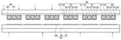
도 1은 본 발명의 한 실시예에 따른 전기 영동 표시 장치의 구조를 도시한 배치도이고, 도 2는 도 1의 전기 영동 표시 장치를 II-II' 선에 따라 자른 단면도이고, 도 3은 본 발명의 한 실시예에 따른 전기 영동 표시 장치의 3개의 화소 영역을 도시한 단면도이다.1 is a layout view illustrating a structure of an electrophoretic display device according to an exemplary embodiment of the present invention, FIG. 2 is a cross-sectional view of the electrophoretic display device of FIG. 1 taken along line II-II ′, and FIG. 3 is a cross-sectional view illustrating three pixel areas of an electrophoretic display device according to an exemplary embodiment.
본 발명의 한 실시예에 따른 전기 영동 표시 장치는 박막 트랜지스터 표시판(100)과 이와 마주보고 있는 공통 전극 표시판(200) 및 양 표시판(100, 200) 사 이에 위치하며 레이저 열 전사(laser induced thermal imaging; LITI)법에 의해 형성된 전기 영동부(300)을 포함한다.The electrophoretic display device according to an exemplary embodiment of the present invention is positioned between the thin film
먼저, 박막 트랜지스터 표시판(100)에 대해 설명한다.First, the thin film
도 1 내지 도 3에서 도시한 바와 같이, 투명한 유리 등으로 이루어진 절연 기판(110) 위에 게이트 신호를 전달하는 복수의 게이트선(gate line)(121)이 형성되어 있다. 게이트선(121)은 가로 방향으로 뻗어 있으며, 각 게이트선(121)은 복수의 게이트 전극(gate electrode)(124) 및 다른 층이나 외부 회로와의 연결을 위한 넓은 끝부분(129)을 포함한다.As illustrated in FIGS. 1 to 3, a plurality of
게이트선(121)은 알루미늄과 알루미늄 합금 등 알루미늄 계열의 금속, 은과 은 합금 등 은 계열의 금속, 구리와 구리 합금 등 구리 계열의 금속, 몰리브덴과 몰리브덴 합금 등 몰리브덴 계열의 금속, 크롬, 티타늄, 탄탈륨 따위로 이루어지는 것이 바람직하다. 게이트선(121)은 물리적 성질이 다른 두 개의 막, 즉 하부막(도시하지 않음)과 그 위의 상부막(도시하지 않음)을 포함할 수 있다. 상부막은 게이트선(121)의 신호 지연이나 전압 강하를 줄일 수 있도록 낮은 비저항(resistivity)의 금속, 예를 들면 알루미늄(Al)이나 알루미늄 합금 등 알루미늄 계열의 금속으로 이루어진다. 이와는 달리, 하부막은 다른 물질, 특히 ITO(indium tin oxide) 및 IZO(indium zinc oxide)와의 접촉 특성이 우수한 물질, 이를테면 몰리브덴(Mo), 몰리브덴 합금, 크롬(Cr) 등으로 이루어진다. 하부막과 상부막의 조합의 예로는 크롬/알루미늄-네오디뮴(Nd) 합금을 들 수 있다.The
게이트선(121)은 단일막 구조를 가지거나 세 층 이상을 포함할 수 있다.The
게이트선(121) 위에는 질화규소(SiNx) 따위로 이루어진 게이트 절연막(gate insulating layer)(140)이 형성되어 있다.A
게이트 절연막(140) 상부에는 수소화 비정질 규소(hydrogenated amorphous silicon) 등으로 이루어진 복수의 선형 반도체층(151)이 형성되어 있다. 선형 반도체층(151)은 세로 방향으로 뻗어 있으며, 게이트 전극(124)을 향하여 뻗어 나온 복수의 돌출부(extension)(154)를 포함한다. 또한, 선형 반도체층(151)은 게이트선(121)과 만나는 지점 부근에서 폭이 커져서 게이트선(121)의 넓은 면적을 덮고 있다.A plurality of linear semiconductor layers 151 made of hydrogenated amorphous silicon or the like are formed on the
반도체층(151)의 상부에는 실리사이드(silicide) 또는 n형 불순물이 고농도로 도핑되어 있는 n+ 수소화 비정질 규소 따위의 물질로 이루어진 복수의 선형 및 섬형 저항성 접촉 부재(ohmic contact)(161, 165)가 형성되어 있다. 선형 접촉 부재(161)는 복수의 돌출부(163)를 가지고 있으며, 상기 돌출부(163)와 섬형 접촉 부재(165)는 쌍을 이루어 반도체층(151)의 돌출부(154) 위에 위치한다.A plurality of linear and island ohmic
저항성 접촉 부재(163, 165) 및 게이트 절연막(140) 위에는 각각 복수의 데이터선(data line)(171), 복수의 드레인 전극(drain electrode)(175)이 형성되어 있다.A plurality of
데이터선(171)은 세로 방향으로 뻗어 게이트선(121)과 교차하며 데이터 전압(data voltage)을 전달한다. 각 데이터선(171)은 게이트 전극(124)을 향하여 뻗어 J자형으로 굽은 복수의 소스 전극(source electrode)(173)과 다른 층 또는 외부 구동 회로와의 접속을 위한 넓은 끝부분(179)을 포함한다. 한 쌍의 소스 전 극(173)과 드레인 전극(175)은 서로 분리되어 있으며 게이트 전극(124)에 대하여 서로 반대쪽에 위치되어 있다.The
데이터선(171) 및 드레인 전극(175)은 크롬 또는 몰리브덴 계열의 금속, 탄탈륨 및 티타늄 등 내화성 금속으로 이루어지는 것이 바람직하며, 몰리브덴(Mo), 몰리브덴 합금, 크롬(Cr) 따위의 하부막(도시하지 않음)과 그 위에 위치한 알루미늄 계열 금속인 상부막(도시하지 않음)으로 이루어진 다층막 구조를 가질 수 있다.The
게이트 전극(124), 소스 전극(173) 및 드레인 전극(175)은 반도체층(151)의 돌출부(154)와 함께 박막 트랜지스터(Thin Film Transistor, TFT)를 이루며, 박막 트랜지스터의 채널(channel)은 소스 전극(173)과 드레인 전극(175) 사이의 돌출부(154)에 형성되어 있다.The
저항성 접촉 부재(161, 165)는 그 아래의 반도체층(151)과 그 상부의 소스 전극(173) 및 드레인 전극(175) 사이에 존재하며 접촉 저항을 낮추어 주는 역할을 한다.The
선형 반도체층(151)은 소스 전극(173)과 드레인 전극(175) 사이를 비롯하여 데이터선(171) 및 드레인 전극(175)에 가리지 않고 노출된 부분을 가지고 있으며, 대부분의 영역에서 선형 반도체층(151)의 폭이 데이터선(171)의 폭보다 작지만 전술한 바와 같이 게이트선(121)과 만나는 부분에서 폭이 커져서 게이트선(121)과 데이터선(171) 사이의 절연을 강화한다.The
데이터선(171), 드레인 전극(175) 및 노출된 반도체층(151) 위에는 평탄화 특성이 우수하며 감광성(photosensitivity)을 가지는 유기 물질, 플라즈마 화학 기 상 증착(Plasma Enhanced Chemical Vapor Deposition, PECVD)으로 형성되는 a-Si:C:O, a-Si:O:F 등의 저유전율 절연 물질, 또는 무기 물질인 질화 규소(SiNx) 따위로 이루어진 보호막(passivation layer)(180)이 단일층 또는 복수층으로 형성되어 있다. 예컨대, 유기 물질로 형성하는 경우에는 소스 전극(173)과 드레인 전극(175) 사이의 반도체층(154)이 노출된 부분으로 보호막(180)의 유기 물질이 접촉하는 것을 방지하기 위하여, 유기막의 하부에 질화규소(SiNx) 또는 산화규소(SiO2)로 이루어진 절연막(도시하지 않음)이 추가로 형성될 수도 있다.On the
보호막(180)에는 게이트선(121)의 끝부분(129), 드레인 전극(175) 및 데이터선(171)의 끝부분(179)을 각각 노출시키는 복수의 접촉구(contact hole)(181, 185, 182)가 형성되어 있다.The
보호막(180) 위에는 ITO 또는 IZO로 이루어지거나 불투명한 금속으로 이루어진 복수의 화소 전극(pixel electrode)(190) 및 복수의 접촉 보조 부재(contact assistant)(81, 82)가 형성되어 있다.On the
화소 전극(190)은 접촉구(185)를 통하여 드레인 전극(175)과 물리적ㅇ전기적으로 연결되어 드레인 전극(175)으로부터 데이터 전압을 받아 각 전기 영동 부재 (320, 321, 322)에 데이터 전압을 인가한다.The
접촉 보조 부재(81, 82)는 접촉구(181, 182)를 통하여 게이트선(121)의 끝부분(129) 및 데이터선(171)의 끝부분(179)과 각각 연결된다. 접촉 보조 부재(81, 82)는 게이트선(121) 및 데이터선(171)의 끝부분과 구동 집적 회로와 같은 외부 장 치와의 접착성을 보완하고 이들을 보호한다.The contact
다음으로 전기 영동부(300)를 설명한다.Next, the
전기 영동부(300)는 각각의 화소 전극(190) 위에 레이저 열 전사(laser induced thermal imaging; LITI)법에 의해 형성되어 있는 전사 필름(310, 311, 312)과 각 전사 필름(310, 311, 312) 내에 분산 고정되어 있는 전기 영동 부재(320, 321, 322)를 포함한다.The
전사 필름(310, 311, 312)은 서로 다른 복수의 화소 전극(190) 위에 교대로 반복적으로 배치되어 있는 제1 전사 필름(310), 제2 전사 필름(311), 제3 전사 필름(312)을 포함하며, 자외선 경화제(316)를 포함하는 유기 필름으로 이루어져 있다.The
전기 영동 부재(320, 321, 322)는 서로 다른 복수의 화소 전극(190) 위에 교대로 반복적으로 배치되어 있는 제1 전기 영동 부재(320), 제2 전기 영동 부재(321) 및 제3 전기 영동 부재(322)를 포함한다.The
제1 전사 필름(310) 내에 분산 고정 되어 있는 제1 전기 영동 부재(320)는 적색 전기 영동 입자(323), 검은색 전기 영동 입자(326), 전기 영동 입자(323, 326)가 분산되어 있는 분산매(327) 및 이들(323, 326, 327)을 가두고 있는 캡슐(capsule, 329)을 포함한다.The
적색 전기 영동 입자(323)는 적색을 나타내며, 음의 전하를 띄는 대전 입자이다.The red
검은색 전기 영동 입자(326)는 검은색을 나타내며, 양의 전하를 띄는 대전 입자이다.The black
적색 전기 영동 입자(323) 및 검은색 전기 영동 입자(326)는 상기와 반대로 각각 양의 전하와 음의 전하를 띌 수도 있다.The red
제2 전사 필름(311) 내에 분산 고정 되어 있는 제2 전기 영동 부재(321) 및 제3 전사 필름(312) 내에 분산 고정 되어 있는 제3 전기 영동 부재(322)는 적색 전기 영동 입자(323) 대신에 각각 녹색 전기 영동 입자(324)와 청색 전기 영동 입자(325)를 포함하는 것을 제외하고는 제1 전기 영동 부재(320)와 동일하다.The
여기서, 녹색 전기 영동 입자(324)는 녹색을 나타내며, 음의 전하를 띄는 대전 입자이다. 또한 청색 전기 영동 입자(325)는 청색을 나타내며, 음의 전하를 띄는 대전 입자이다.Here, the green
제2 전기 영동 부재(321)의 녹색 전기 영동 입자(324) 및 검은색 전기 영동 입자(326)는 상기와 반대로 각각 양의 전하와 음의 전하를 띌 수도 있다. 또한 제3 전기 영동 부재(322)의 청색 전기 영동 입자(325) 및 검은색 전기 영동 입자(326)의 경우도 마찬가지로 각각 양의 전하와 음의 전하를 띌 수도 있다.The green
한편 적색 전기 영동 입자(323), 녹색 전기 영동 입자(324) 및 청색 전기 영동 입자(325)는 각각 노란색을 갖는 전기 영동 입자, 마젠타(magenta)를 갖는 전기 영동 입자, 시안(cyan)을 갖는 전기 영동 입자로 대체되어도 무방하다.Meanwhile, the red
분산매(327)는 각 전기 영동 입자(323, 324, 325, 326)를 분산하며, 투명색이나검은색을 띌 수 있다. 분산매(327)가 검은색을 띄는 경우 분산매(327)를 이용하여 검은색을 표현할 수 있기 때문에 각 전기 영동 부재(320, 321, 322)에 포함된 검은색 전기 영동 입자(326)는 생략할 수 있다.The
캡슐(329)은 각 전기 영동 입자(323, 324, 325, 326)와 분산매(327)를 가두고 있으며 이로 인해 각 전기 영동 입자(323, 324, 325, 326)는 캡슐(329) 내부에서만 색상 표현을 위한 유동이 가능하다.The
다음으로 공통 전극 표시판(200)에 대해 설명한다.Next, the common
공통 전극 표시판(200)은 전기 영동부(300) 위에 형성되어 있으며, 투명한 절연 기판(210)과 절연 기판(210) 위에 형성되어 있는 공통 전극(220)을 포함한다.The common
공통 전극(220)은 ITO 또는 IZO 이루어진 투명 전극으로서 각 전기 영동 부재 (320, 321, 322)에 공통 전압을 인가한다.The
공통 전압(common voltage)을 인가하는 공통 전극(220)은 데이터 전압을 인가하는 화소 전극(190)과 함께 각 전기 영동 부재 (320, 321, 322)에 전기장을 생성한다. 생성된 전기장은 각 전사 필름(310, 311, 312)에 의해 분산 고정되어 있는 각 전기 영동 부재(320, 321, 322)의 전기 영동 입자(323, 324, 325, 326)의 위치를 변화시켜 원하는 색상의 화상을 표시한다.The
이하에서는 본 발명의 한 실시예에 따른 전기 영동 표시 장치가 여러 가지 색상의 화상을 표시하는 방법에 대해 구체적으로 설명한다.Hereinafter, a method of displaying an image of various colors by the electrophoretic display device according to an exemplary embodiment of the present invention will be described in detail.
전기 영동 표시 장치의 드레인 전극(175)을 통해 화소 전극(190)에 음의 전압이 인가되고 공통 전극(220)에 양의 전압이 인가되는 경우를 설명한다.A case in which a negative voltage is applied to the
이 경우 캡슐(329) 내의 분산매(327)에 불규칙하게 분산되어 있으며 음 전하를 띄는 적색, 녹색, 청색 전기 영동 입자(323, 324, 325)는 양의 전압이 인가된 공통 전극(220)으로 이동하여 배열하게 된다. 한편, 양 전하를 띄는 검은색 전기 영동 입자(326)는 음의 전압이 인가된 화소 전극(190)으로 이동하여 배열하게 된다. 이러한 배열에 의해 공통 전극 표시판(200)을 통과하여 입사된 외부광은 각 전기 영동 입자(323, 324, 325)에 의해 반사되면서 화소 영역 별로 각 전기 영동 입자(323, 324, 325)가 띄는 각각의 색상을 외부로 표시한다. 이때 흰색은 적색, 녹색, 청색 전기 영동 입자(323, 324, 325)가 표시하는 각 색상의 가법 혼색을 통해 표시된다.In this case, the red, green, and blue
다음으로 전기 영동 표시 장치의 드레인 전극(175)을 통해 화소 전극(190)에 양의 전압이 인가되고 공통 전극(220)에 음의 전압이 인가되는 경우를 설명한다.Next, a case in which a positive voltage is applied to the
이 경우 분산매(327)에 불규칙하게 분산되어 있으며 각각 음 전하를 띄는 적색, 녹색, 청색 전기 영동 입자(323, 324, 325)는 양의 전압이 인가된 화소 전극(190)으로 이동하여 배열하게 된다. 한편 양 전하를 띄는 검은색 전기 영동 입자(326)는 음의 전압이 인가된 공통 전극(220)으로 이동하여 배열하게 된다.In this case, the red, green, and blue
이러한 배열로 인해 외부로부터 공통 전극 표시판(200)을 통과하여 입사된 외부광은 검은색 전기 영동 입자(326)에 흡수되면서 검은색을 표시한다.Due to this arrangement, the external light incident through the
한편, 각 화소 전극(190)은 서로 다른 크기의 양 또는 음의 전압을 인가할 수 있기 때문에 각 화소 전극(190) 별로 각 전기 영동 입자(323, 324, 325, 326)의 배열을 다르게 할 수 있다. 이를 통해 원하는 색상의 표현이 가능하게 된다.On the other hand, since each
이하에서는 본 발명의 한 실시예에 따른 전기 영동 표시 장치의 제조 방법에 대하여 도 1 내지 도 3 및 도 4a 내지 도 4i를 참조하여 상세히 설명한다.Hereinafter, a method of manufacturing an electrophoretic display device according to an exemplary embodiment of the present invention will be described in detail with reference to FIGS. 1 to 3 and 4A to 4I.
도 4a 내지 도 4i는 본 발명의 한 실시예에 따른 전기 영동 표시 장치의 제조 방법을 순차적으로 도시한 단면도이다.4A through 4I are cross-sectional views sequentially illustrating a method of manufacturing an electrophoretic display device according to an exemplary embodiment of the present invention.
먼저, 도 4a에 도시한 바와 같이 제1 전사용 기판(10) 위에 열 변환막(20)을 형성한다. 또한 제2 전사용 기판(도 4f의 11에 해당) 및 제3 전사용 기판(도 4h의 12에 해당) 위에도 각각 열 변환막(20)을 형성한다.First, as illustrated in FIG. 4A, a
여기서 각 전사용 기판(10, 11, 12)은 투명한 유리 또는 플라스틱 등으로 이루어진 절연 기판이다.Here, each
열 변환막(20)은 각 전사용 기판(10, 11, 12)으로 조사된 레이저의 빛 에너지를 열에너지로 바꾸어 열에너지를 각 전사 필름(310, 311, 312)의 일부에 공급한다. 이에 따라 전사 필름(310, 311, 312) 중 열에너지를 공급 받은 부분은 공급된 열에 의해 유동성을 가지게 되어 공통 전극 표시판(200)으로 전사된다.The
열 변환막(20)은 코팅에 의해 형성된 프탈로 시아닌(phthalocyanine) 또는 나프탈로 시아닌 (naphtalocyanine) 등의 유기물일 수 있다. 또한 열 변환막(20)은 증착에 의해 형성되며 검은색을 갖는(blackened) 은(Ag) 등의 금속 등을 포함할 수 있다.The
그런 다음 도 4b에 도시한 바와 같이 제1 전사용 기판(10) 위에 형성된 열 변환막(20) 위에 적색 및 검은색 전기 영동 입자(323, 326)를 포함하는 제1 전기 영동 부재(320) 및 자외선 경화제(316)가 분산된 액상 또는 젤 상태의 전사 필름 형성 물질(315)을 도포 부재(30)를 이용하여 도포한다.Then, as shown in FIG. 4B, the
마찬가지 방법으로 제2 전사용 기판(11) 위에 형성된 열 변환막(20) 위에 녹 색 및 검은색 전기 영동 입자(324, 326)를 포함하는 제2 전기 영동 부재(321) 및 자외선 경화제(316)가 포함된 액상 또는 젤 상태의 전사 필름 형성 물질(315)을 도포 부재(30)를 이용하여 도포한다.In the same manner, the
또한 제3 전사용 기판(12) 위에 형성된 열 변환막(20) 위에 청색 및 검은색 전기 영동 입자(325, 326)를 포함하는 제3 전기 영동 부재(322) 및 자외선 경화제(316)가 포함된 액상 또는 젤 상태의 전사 필름 형성 물질(315)을 도포 부재(30)를 이용하여 도포한다.In addition, the
그런 다음 도 4c에 도시한 바와 같이 제1 전사용 기판(10) 위에 도포된 액상 또는 젤 상태의 전사 필름 형성 물질(315)을 자외선을 이용하여 경화함으로써 경화된 제1 전사 필름(310)을 형성한다.Then, as shown in FIG. 4C, the hardened
마찬가지 방법으로 제2 전사용 기판(11) 및 제3 전사용 기판(12) 위에 도포된 액상 또는 젤 상태의 전사 필름 형성 물질(315)을 자외선을 이용하여 경화함으로써 각각 경화된 제2 전사 필름(311, 도 4f 참조) 및 제3 전사 필름(312, 도4h 참조)를 형성한다.In the same manner, the second transfer film cured by curing the transfer
각 전사 필름(310, 311, 312)의 경화는 자외선을 이용하지 않고 건조에 의해서도 가능하다.Hardening of each
그런 다음 도 4d에 도시한 바와 같이 공통 전극(220)이 형성되어 있는 공통 전극 표시판(200)을 마련한 후, 공통 전극(220)과 제1 전사 필름(310)이 마주하도록 공통 전극 표시판(200) 위에 제1 전사용 기판(10)을 정렬한 후, 도 4e에서 보는 바와 같이 레이저 열 전사(laser induced thermal imaging; LITI)법에 의해 제1 전 사 필름(310)의 소정 부분을 공통 전극(220)의 대응 부분 위로 전사한다.Then, as shown in FIG. 4D, after the common
여기서, 공통 전극(220)의 대응 부분은 후속 공정에 의해 마주하는 복수의 화소 전극(190) 중에서 제1 전기 영동 부재(320)가 위치하게 되는 화소 전극(190)에 대응되는 부분이기도 하다.Here, the corresponding portion of the
레이저 열 전사(laser induced thermal imaging; LITI)법에 의해 제1 전사 필름(310)의 소정 부분을 공통 전극(220)의 대응 부분 위로 전사하는 과정을 자세히 살펴본다.A process of transferring a predetermined portion of the
먼저 레이저 조사 부재(미도시)를 이용하여 공통 전극 표시판(200)의 상부에서 제1 전사 필름(310)의 소정 부분을 향해 레이저를 조사한다. 레이저 조사 부재(미도시)에 의해 조사되는 레이저는 이에 한정되는 것은 아니나 에너지의 강도 및 조사 시간 등을 고려하여 파장이 760nm 내지 1200nm 를 갖는 적외선 레이저가 바람직하다.First, a laser is irradiated toward a predetermined portion of the
제1 전사 필름(310)의 소정 부분을 향해 조사된 레이저는 투명한 제1 전사용 기판(10)을 통과한 후 열 변환막(20)의 소정 부분에 조사되게 된다. 레이저가 조사된 열 변환막(20)의 소정 부분은 레이저의 빛 에너지를 열 에너지로 변환하여 변환된 열 에너지를 제1 전사 필름(310)의 소정 부분으로 공급하게 된다. 이에 따라 열 변환막(20)의 소정 부분으로부터 열을 공급받은 제1 전사 필름(310)의 대응 부분은 경화 상태를 유지하는 제1 전사 필름(310)의 다른 부분과 달리 유동성을 가지게 되어 아래로 이탈함으로써 공통 전극(220)의 소정 부분 위로 전사되게 된다. 전사되는 제1 전사 필름(310)은 제1 전기 영동 부재(320)을 포함하고 있기 때문에 제 1 전기 영동 부재(320)도 함께 공통 전극(220)의 소정 부분으로 전사된다.The laser irradiated toward a predetermined portion of the
그런 다음 전사된 제1 전사 필름(310)의 소정 부분에 자외선을 조사하여 경화하면 공통 전극(220)의 소정 부분에 각각 적색 또는 검은색 색상을 표현할 수 있는 제1 전기 영동 부재(320)가 부착된다. 한편 전사된 제1 전사 필름(310)의 소정 부분의 경화는 자외선을 이용하지 않고 건조에 의해 이루어질 수도 있다.Then, when a predetermined portion of the transferred
이 후 도 4f에 도시한 바와 같이 공통 전극(220)과 제2 전사 필름(311)이 마주하도록 공통 전극 표시판(200) 위에 제2 전사용 기판(11)을 정렬한 후, 도 4g에 도시한 바와 같이 레이저 열 전사(laser induced thermal imaging; LITI)법에 의해 제2 전사 필름(311)의 소정 부분을 전사된 제1 전사 필름(310)의 소정 부분에 이웃하도록 공통 전극(220)의 소정 부분으로 전사하고 경화한다. 이를 통해 공통 전극(220)의 소정 부분에 제1 전기 영동 부재(320)와 이웃하는 제2 전기 영동 부재(321)가 부착된다.Thereafter, as illustrated in FIG. 4F, the
그런 다음 도 4h에 도시한 바와 같이 공통 전극(220)과 제3 전사 필름(312)이 마주하도록 공통 전극 표시판(200) 위에 제3 전사용 기판(12)을 정렬한 후, 도 4i에 도시한 바와 같이 레이저 열 전사(laser induced thermal imaging; LITI)법에 의해 제3 전사 필름(312)의 소정 부분을 전사된 제1 전사 필름(310)의 소정 부분 및 전사된 제2 전사 필름(311)의 소정 부분에 각각 이웃하도록 공통 전극(220)의 소정 부분으로 전사하고 경화한다. 이를 통해 공통 전극(220)의 소정 부분에 제1 전기 영동 부재(320) 및 제 2전기 영동 부재(321)와 각각 이웃하는 제3 전기 영동 부재(322)가 부착된다. 이를 통해 전기 영동부(300)가 완성된다.Then, as illustrated in FIG. 4H, the
이 후 도 4j에 도시한 바와 같이 공지의 방법으로 제조된 박막 트랜지스터 표시판(100)을 마련하여 전기 영동부(300)의 제1 내지 제3 전사 필름(310, 311, 312) 중 어느 하나가 각 화소 전극(190)에 대응 위치하도록 양 표시판(100, 200)을 정렬하고 상호 가압한다. 가압을 통해 각 화소 전극(190)과 제1 내지 제3 전사 필름(310, 311, 312) 중 어느 하나를 각각 상호 밀착하면 도 1 내지 도 3에 도시한 본 발명의 한 실시예에 따른 전기 영동 표시 장치가 완성된다.Thereafter, as shown in FIG. 4J, a thin film
본 발명의 한 실시예에 따른 전기 영동 표시 장치의 제조 방법에 의하면, 레이저 열 전사(laser induced thermal imaging; LITI)법을 이용하여 용이하게 각 화소 전극(190)과 공통 전극 사이에 전기 영동 부재(320, 321, 322)를 형성할 수 있다. 따라서 전기 영동 표시 장치의 제조 효율 및 제조의 정확도를 향상시킬 수 있다. 또한 이를 통해 제조 효율과 표시 성능이 우수한 전기 영동 표시 장치가 제공된다.According to a method of manufacturing an electrophoretic display device according to an exemplary embodiment of the present invention, an electrophoretic member (e.g., a gap between a
이하에서는 본 발명의 한 실시예에 따른 전기 영동 표시 장치의 다른 제조 방법을 도 5를 참조하여 설명한다.Hereinafter, another manufacturing method of an electrophoretic display device according to an exemplary embodiment of the present invention will be described with reference to FIG. 5.
도 5는 본 발명의 한 실시예에 따른 전기 영동 표시 장치의 다른 제조 방법을 나타낸 단면도이다.5 is a cross-sectional view illustrating another manufacturing method of an electrophoretic display device according to an exemplary embodiment of the present invention.
도 5에 도시한 본 발명의 한 실시예에 따른 전기 영동 표시 장치의 다른 제조 방법은 공통 전극(220)이 아닌 박막 트랜지스터 표시판(100)의 각 화소 전극(190)에 제1 내지 제3 전사 필름(310, 311, 312) 중 어느 하나를 레이저 열 전사(laser induced thermal imaging; LITI)법에 의해 전사하며, 전사된 제1 내지 제 3 전사 필름(310, 311, 312)과 공통 전극(220)을 상호 밀착하는 것을 제외하고는 도 4a 내지 4j에 도시한 본 발명의 한 실시예에 따른 전기 영동 표시 장치의 제조 방법과 동일하다.Another manufacturing method of the electrophoretic display device according to the exemplary embodiment illustrated in FIG. 5 may include first to third transfer films on the
도 5에 도시한 본 발명의 한 실시예에 따른 전기 영동 표시 장치의 다른 제조 방법에 의해서도 도 4a 내지 4j에 도시한 본 발명의 한 실시예에 따른 전기 영동 표시 장치의 제조 방법과 동일한 효과를 얻을 수 있다.Another manufacturing method of the electrophoretic display device according to the exemplary embodiment shown in FIG. 5 may have the same effect as the manufacturing method of the electrophoretic display apparatus according to the exemplary embodiment shown in FIGS. 4A to 4J. Can be.
이하에서는 본 발명의 다른 실시예에 따른 전기 영동 표시 장치를 도 6을 참조하여 설명한다. 도 6은 본 발명의 다른 실시예에 따른 전기 영동 표시 장치의 3개의 화소 영역을 도시한 단면도이다.Hereinafter, an electrophoretic display device according to another exemplary embodiment of the present invention will be described with reference to FIG. 6. 6 is a cross-sectional view illustrating three pixel areas of an electrophoretic display device according to another exemplary embodiment.
본 발명의 다른 실시예에 따른 전기 영동 표시 장치는 전기 영동부(301)의 전기 영동 부재(330)가 모두 흰색을 표시하는 흰색 전기 영동 입자(328)와 검은색을 표시하는 검은색 전기 영동 입자(326)를 포함하는 것을 제외하고는 도 1 내지 도 3에 도시한 본 발명의 한 실시예에 따른 전기 영동 표시 장치와 동일하다.In the electrophoretic display device according to another exemplary embodiment of the present invention, all of the
따라서 본 발명의 다른 실시예에 따른 전기 영동 표시 장치는 본 발명의 한 실시예에 도시한 전기 영동 표시 장치와 달리 흑백 색상 표현만이 가능하다.Accordingly, the electrophoretic display device according to another exemplary embodiment of the present invention may display only black and white colors, unlike the electrophoretic display device illustrated in the exemplary embodiment of the present invention.
이하에서는 본 발명의 다른 실시예에 따른 전기 영동 표시 장치의 제조 방법을 도 7 및 도 8을 참조하여 설명한다.Hereinafter, a method of manufacturing an electrophoretic display device according to another exemplary embodiment of the present invention will be described with reference to FIGS. 7 and 8.
도 7 및 도 8은 본 발명의 다른 실시예에 따른 전기 영동 표시 장치의 제조 방법을 순차적으로 도시한 단면도이다.7 and 8 are cross-sectional views sequentially illustrating a method of manufacturing an electrophoretic display device according to another exemplary embodiment of the present invention.
본 발명의 다른 실시예에 따른 전기 영동 표시 장치는 앞서 설명한 바와 같 이전기 영동부(301)의 전기 영동 부재(330)가 모두 흰색을 표시하는 흰색 전기 영동 입자(328)와 검은색을 표시하는 검은색 전기 영동 입자(326)를 포함하고 있다. 따라서 그 제조 방법은 도 7에 도시한 바와 같이 하나의 전사용 기판(13)에만 열 변환막(20)을 형성하고 열 변환막(20) 위에 도포 및 경화 공정을 통해 전기 영동 부재(330)를 분산 고정하는 전사 필름(313)을 형성하면 된다.In the electrophoretic display device according to another embodiment of the present invention, as described above, the
그런 다음 도 8에 도시한 바와 같이 레이저 열 전사(laser induced thermal imaging; LITI)법에 의해 전사용 기판(13) 위에 형성된 전사 필름(313)의 소정 부분을 공통 전극(220)의 대응 부분으로 한번의 전사 공정을 통해 전사하여 전기 영동부(301)를 형성할 수 있다.Then, as shown in FIG. 8, a predetermined portion of the
본 발명의 다른 실시예에 따른 전기 영동 표시 장치 및 그 제조 방법에 의해서도 본 발명의 한 실시예에 따른 전기 영동 표시 장치 및 그 제조 방법과 동일한 효과를 얻을 수 있다.An electrophoretic display device and a method of manufacturing the same according to another exemplary embodiment of the present invention may have the same effects as those of the electrophoretic display and the method of manufacturing the same.
이상에서 본 발명의 바람직한 실시예에 대하여 상세하게 설명하였지만 본 발명의 권리범위는 이에 한정되는 것은 아니고 다음의 청구범위에서 정의하고 있는 본 발명의 기본 개념을 이용한 당업자의 여러 변형 및 개량 형태 또한 본 발명의 권리범위에 속하는 것이다.Although the preferred embodiments of the present invention have been described in detail above, the scope of the present invention is not limited thereto, and various modifications and improvements of those skilled in the art using the basic concepts of the present invention defined in the following claims are also provided. It belongs to the scope of rights.
이상과 같이, 본 발명에 의하면, 제조 효율과 표시 성능이 우수한 전기 영동 표시 장치 및 그 제조 방법이 제공된다.As mentioned above, according to this invention, the electrophoretic display apparatus excellent in manufacturing efficiency and display performance, and its manufacturing method are provided.
Claims (24)
Translated fromKoreanPriority Applications (2)
| Application Number | Priority Date | Filing Date | Title |
|---|---|---|---|
| KR1020060088033AKR20080023907A (en) | 2006-09-12 | 2006-09-12 | Electrophoretic display device and manufacturing method thereof |
| US11/853,620US20080062119A1 (en) | 2006-09-12 | 2007-09-11 | Electrophoretic display and method of manufacture |
Applications Claiming Priority (1)
| Application Number | Priority Date | Filing Date | Title |
|---|---|---|---|
| KR1020060088033AKR20080023907A (en) | 2006-09-12 | 2006-09-12 | Electrophoretic display device and manufacturing method thereof |
Publications (1)
| Publication Number | Publication Date |
|---|---|
| KR20080023907Atrue KR20080023907A (en) | 2008-03-17 |
Family
ID=39169088
Family Applications (1)
| Application Number | Title | Priority Date | Filing Date |
|---|---|---|---|
| KR1020060088033AWithdrawnKR20080023907A (en) | 2006-09-12 | 2006-09-12 | Electrophoretic display device and manufacturing method thereof |
Country Status (2)
| Country | Link |
|---|---|
| US (1) | US20080062119A1 (en) |
| KR (1) | KR20080023907A (en) |
Cited By (2)
| Publication number | Priority date | Publication date | Assignee | Title |
|---|---|---|---|---|
| KR100925272B1 (en)* | 2008-11-14 | 2009-11-05 | 한국생산기술연구원 | Method and apparatus for fine particle injection of electronic paper using laser |
| KR100937150B1 (en)* | 2008-06-04 | 2010-01-15 | 한국생산기술연구원 | Electronic paper display device manufacturing method |
Families Citing this family (3)
| Publication number | Priority date | Publication date | Assignee | Title |
|---|---|---|---|---|
| WO2011048923A1 (en)* | 2009-10-21 | 2011-04-28 | Semiconductor Energy Laboratory Co., Ltd. | E-book reader |
| TWI600958B (en)* | 2012-03-09 | 2017-10-01 | 元太科技工業股份有限公司 | Electrophoretic display panel and manufacturing method thereof |
| JP7335388B2 (en)* | 2021-01-05 | 2023-08-29 | イー インク コーポレイション | The process of producing electro-optic displays |
Family Cites Families (7)
| Publication number | Priority date | Publication date | Assignee | Title |
|---|---|---|---|---|
| JP4590663B2 (en)* | 1999-10-29 | 2010-12-01 | セイコーエプソン株式会社 | Manufacturing method of color filter |
| US6933098B2 (en)* | 2000-01-11 | 2005-08-23 | Sipix Imaging Inc. | Process for roll-to-roll manufacture of a display by synchronized photolithographic exposure on a substrate web |
| US6545797B2 (en)* | 2001-06-11 | 2003-04-08 | Sipix Imaging, Inc. | Process for imagewise opening and filling color display components and color displays manufactured thereof |
| US7158282B2 (en)* | 2000-03-03 | 2007-01-02 | Sipix Imaging, Inc. | Electrophoretic display and novel process for its manufacture |
| JP4059034B2 (en)* | 2001-08-20 | 2008-03-12 | セイコーエプソン株式会社 | Electrophoresis device, electronic apparatus, and method of manufacturing the electrophoresis device |
| US7038656B2 (en)* | 2002-08-16 | 2006-05-02 | Sipix Imaging, Inc. | Electrophoretic display with dual-mode switching |
| KR101133759B1 (en)* | 2004-12-28 | 2012-04-09 | 삼성전자주식회사 | Electrophoretic indication Display and Method for Manufacturing the same |
- 2006
- 2006-09-12KRKR1020060088033Apatent/KR20080023907A/ennot_activeWithdrawn
- 2007
- 2007-09-11USUS11/853,620patent/US20080062119A1/ennot_activeAbandoned
Cited By (2)
| Publication number | Priority date | Publication date | Assignee | Title |
|---|---|---|---|---|
| KR100937150B1 (en)* | 2008-06-04 | 2010-01-15 | 한국생산기술연구원 | Electronic paper display device manufacturing method |
| KR100925272B1 (en)* | 2008-11-14 | 2009-11-05 | 한국생산기술연구원 | Method and apparatus for fine particle injection of electronic paper using laser |
Also Published As
| Publication number | Publication date |
|---|---|
| US20080062119A1 (en) | 2008-03-13 |
Similar Documents
| Publication | Publication Date | Title |
|---|---|---|
| KR101765274B1 (en) | Liquid crystal display panel | |
| KR20080030154A (en) | Method of driving electrophoretic display | |
| US7436578B2 (en) | Electrophoretic display and manufacturing method thereof | |
| US10032809B2 (en) | Method of manufacturing display device including light blocking portion on planarization layer protrusion | |
| US8049952B2 (en) | Electrophoretic display and the manufacturing method thereof | |
| KR20080023913A (en) | Electrophoretic display device and driving method thereof | |
| CN101276118B (en) | Display device and method of manufacturing the same | |
| KR101598540B1 (en) | Reflective display device and method of manufacturing the same | |
| US11769758B2 (en) | Light emitting diode array containing a black matrix and an optical bonding layer and method of making the same | |
| KR20080023907A (en) | Electrophoretic display device and manufacturing method thereof | |
| KR101337255B1 (en) | Electrophoretic display and method for manufacturing thereof | |
| US10247992B2 (en) | Display device | |
| JP2007072457A (en) | Liquid crystal display device and manufacturing method thereof | |
| KR20100059448A (en) | Thin film transistor array panel and manufacturing method thereof | |
| KR20080046960A (en) | Electrophoretic display device and manufacturing method thereof | |
| CN100394271C (en) | Color filter substrate for liquid crystal display and method of fabricating the same | |
| KR101747721B1 (en) | Liquid crystal display device and manufacturing method thereof | |
| KR20100076822A (en) | Electrophoretic display device and method for fabricating the same | |
| KR101742125B1 (en) | Method of fabrication electrophoretic display deivce | |
| JP5105776B2 (en) | Method for manufacturing thin film transistor element for liquid crystal display device | |
| KR20080014384A (en) | Electrophoresis display | |
| KR101007689B1 (en) | LCD Display | |
| KR101748702B1 (en) | Composite of partition, electrophoretic display deivce and method of fabrication thereof | |
| KR20090061498A (en) | Manufacturing Method of Electrophoretic Display | |
| KR20030047132A (en) | Method of forming spacers in liquid crystal display device |
Legal Events
| Date | Code | Title | Description |
|---|---|---|---|
| PA0109 | Patent application | Patent event code:PA01091R01D Comment text:Patent Application Patent event date:20060912 | |
| PG1501 | Laying open of application | ||
| PC1203 | Withdrawal of no request for examination | ||
| WITN | Application deemed withdrawn, e.g. because no request for examination was filed or no examination fee was paid |