KR20080010796A - OLED display and driving method thereof - Google Patents
OLED display and driving method thereofDownload PDFInfo
- Publication number
- KR20080010796A KR20080010796AKR1020060071315AKR20060071315AKR20080010796AKR 20080010796 AKR20080010796 AKR 20080010796AKR 1020060071315 AKR1020060071315 AKR 1020060071315AKR 20060071315 AKR20060071315 AKR 20060071315AKR 20080010796 AKR20080010796 AKR 20080010796A
- Authority
- KR
- South Korea
- Prior art keywords
- voltage
- driving
- current
- data
- gray
- Prior art date
- Legal status (The legal status is an assumption and is not a legal conclusion. Google has not performed a legal analysis and makes no representation as to the accuracy of the status listed.)
- Ceased
Links
Images


Classifications
- G—PHYSICS
- G09—EDUCATION; CRYPTOGRAPHY; DISPLAY; ADVERTISING; SEALS
- G09G—ARRANGEMENTS OR CIRCUITS FOR CONTROL OF INDICATING DEVICES USING STATIC MEANS TO PRESENT VARIABLE INFORMATION
- G09G3/00—Control arrangements or circuits, of interest only in connection with visual indicators other than cathode-ray tubes
- G09G3/20—Control arrangements or circuits, of interest only in connection with visual indicators other than cathode-ray tubes for presentation of an assembly of a number of characters, e.g. a page, by composing the assembly by combination of individual elements arranged in a matrix no fixed position being assigned to or needed to be assigned to the individual characters or partial characters
- G09G3/22—Control arrangements or circuits, of interest only in connection with visual indicators other than cathode-ray tubes for presentation of an assembly of a number of characters, e.g. a page, by composing the assembly by combination of individual elements arranged in a matrix no fixed position being assigned to or needed to be assigned to the individual characters or partial characters using controlled light sources
- G09G3/30—Control arrangements or circuits, of interest only in connection with visual indicators other than cathode-ray tubes for presentation of an assembly of a number of characters, e.g. a page, by composing the assembly by combination of individual elements arranged in a matrix no fixed position being assigned to or needed to be assigned to the individual characters or partial characters using controlled light sources using electroluminescent panels
- G09G3/32—Control arrangements or circuits, of interest only in connection with visual indicators other than cathode-ray tubes for presentation of an assembly of a number of characters, e.g. a page, by composing the assembly by combination of individual elements arranged in a matrix no fixed position being assigned to or needed to be assigned to the individual characters or partial characters using controlled light sources using electroluminescent panels semiconductive, e.g. using light-emitting diodes [LED]
- G09G3/3208—Control arrangements or circuits, of interest only in connection with visual indicators other than cathode-ray tubes for presentation of an assembly of a number of characters, e.g. a page, by composing the assembly by combination of individual elements arranged in a matrix no fixed position being assigned to or needed to be assigned to the individual characters or partial characters using controlled light sources using electroluminescent panels semiconductive, e.g. using light-emitting diodes [LED] organic, e.g. using organic light-emitting diodes [OLED]
- G09G3/3225—Control arrangements or circuits, of interest only in connection with visual indicators other than cathode-ray tubes for presentation of an assembly of a number of characters, e.g. a page, by composing the assembly by combination of individual elements arranged in a matrix no fixed position being assigned to or needed to be assigned to the individual characters or partial characters using controlled light sources using electroluminescent panels semiconductive, e.g. using light-emitting diodes [LED] organic, e.g. using organic light-emitting diodes [OLED] using an active matrix
- G09G3/3233—Control arrangements or circuits, of interest only in connection with visual indicators other than cathode-ray tubes for presentation of an assembly of a number of characters, e.g. a page, by composing the assembly by combination of individual elements arranged in a matrix no fixed position being assigned to or needed to be assigned to the individual characters or partial characters using controlled light sources using electroluminescent panels semiconductive, e.g. using light-emitting diodes [LED] organic, e.g. using organic light-emitting diodes [OLED] using an active matrix with pixel circuitry controlling the current through the light-emitting element
- G—PHYSICS
- G09—EDUCATION; CRYPTOGRAPHY; DISPLAY; ADVERTISING; SEALS
- G09G—ARRANGEMENTS OR CIRCUITS FOR CONTROL OF INDICATING DEVICES USING STATIC MEANS TO PRESENT VARIABLE INFORMATION
- G09G2320/00—Control of display operating conditions
- G09G2320/04—Maintaining the quality of display appearance
- G09G2320/043—Preventing or counteracting the effects of ageing
- G09G2320/048—Preventing or counteracting the effects of ageing using evaluation of the usage time
- G—PHYSICS
- G09—EDUCATION; CRYPTOGRAPHY; DISPLAY; ADVERTISING; SEALS
- G09G—ARRANGEMENTS OR CIRCUITS FOR CONTROL OF INDICATING DEVICES USING STATIC MEANS TO PRESENT VARIABLE INFORMATION
- G09G2320/00—Control of display operating conditions
- G09G2320/08—Arrangements within a display terminal for setting, manually or automatically, display parameters of the display terminal
- G—PHYSICS
- G09—EDUCATION; CRYPTOGRAPHY; DISPLAY; ADVERTISING; SEALS
- G09G—ARRANGEMENTS OR CIRCUITS FOR CONTROL OF INDICATING DEVICES USING STATIC MEANS TO PRESENT VARIABLE INFORMATION
- G09G2330/00—Aspects of power supply; Aspects of display protection and defect management
- G09G2330/12—Test circuits or failure detection circuits included in a display system, as permanent part thereof
- G—PHYSICS
- G09—EDUCATION; CRYPTOGRAPHY; DISPLAY; ADVERTISING; SEALS
- G09G—ARRANGEMENTS OR CIRCUITS FOR CONTROL OF INDICATING DEVICES USING STATIC MEANS TO PRESENT VARIABLE INFORMATION
- G09G3/00—Control arrangements or circuits, of interest only in connection with visual indicators other than cathode-ray tubes
- G09G3/20—Control arrangements or circuits, of interest only in connection with visual indicators other than cathode-ray tubes for presentation of an assembly of a number of characters, e.g. a page, by composing the assembly by combination of individual elements arranged in a matrix no fixed position being assigned to or needed to be assigned to the individual characters or partial characters
- G09G3/2092—Details of a display terminals using a flat panel, the details relating to the control arrangement of the display terminal and to the interfaces thereto
- G—PHYSICS
- G09—EDUCATION; CRYPTOGRAPHY; DISPLAY; ADVERTISING; SEALS
- G09G—ARRANGEMENTS OR CIRCUITS FOR CONTROL OF INDICATING DEVICES USING STATIC MEANS TO PRESENT VARIABLE INFORMATION
- G09G3/00—Control arrangements or circuits, of interest only in connection with visual indicators other than cathode-ray tubes
- G09G3/20—Control arrangements or circuits, of interest only in connection with visual indicators other than cathode-ray tubes for presentation of an assembly of a number of characters, e.g. a page, by composing the assembly by combination of individual elements arranged in a matrix no fixed position being assigned to or needed to be assigned to the individual characters or partial characters
- G09G3/22—Control arrangements or circuits, of interest only in connection with visual indicators other than cathode-ray tubes for presentation of an assembly of a number of characters, e.g. a page, by composing the assembly by combination of individual elements arranged in a matrix no fixed position being assigned to or needed to be assigned to the individual characters or partial characters using controlled light sources
- G09G3/30—Control arrangements or circuits, of interest only in connection with visual indicators other than cathode-ray tubes for presentation of an assembly of a number of characters, e.g. a page, by composing the assembly by combination of individual elements arranged in a matrix no fixed position being assigned to or needed to be assigned to the individual characters or partial characters using controlled light sources using electroluminescent panels
- G09G3/32—Control arrangements or circuits, of interest only in connection with visual indicators other than cathode-ray tubes for presentation of an assembly of a number of characters, e.g. a page, by composing the assembly by combination of individual elements arranged in a matrix no fixed position being assigned to or needed to be assigned to the individual characters or partial characters using controlled light sources using electroluminescent panels semiconductive, e.g. using light-emitting diodes [LED]
- G09G3/3208—Control arrangements or circuits, of interest only in connection with visual indicators other than cathode-ray tubes for presentation of an assembly of a number of characters, e.g. a page, by composing the assembly by combination of individual elements arranged in a matrix no fixed position being assigned to or needed to be assigned to the individual characters or partial characters using controlled light sources using electroluminescent panels semiconductive, e.g. using light-emitting diodes [LED] organic, e.g. using organic light-emitting diodes [OLED]
- G09G3/3275—Details of drivers for data electrodes
- G09G3/3291—Details of drivers for data electrodes in which the data driver supplies a variable data voltage for setting the current through, or the voltage across, the light-emitting elements
Landscapes
- Engineering & Computer Science (AREA)
- Physics & Mathematics (AREA)
- Computer Hardware Design (AREA)
- General Physics & Mathematics (AREA)
- Theoretical Computer Science (AREA)
- Control Of El Displays (AREA)
- Electroluminescent Light Sources (AREA)
- Control Of Indicators Other Than Cathode Ray Tubes (AREA)
Abstract
Translated fromKoreanDescription
Translated fromKorean도 1은 본 발명의 한 실시예에 따른 유기 발광 표시 장치의 블록도.1 is a block diagram of an organic light emitting diode display according to an exemplary embodiment of the present invention.
도 2는 본 발명의 한 실시예에 따른 유기 발광 표시 장치의 한 화소에 대한 등가 회로도.2 is an equivalent circuit diagram of one pixel of an organic light emitting diode display according to an exemplary embodiment of the present invention.
도 3은 본 발명의 한 실시예에 따른 유기 발광 표시 장치의 계조 전압 생성부에서 출력되는 기준 계조 전압의 예를 도시하는 그래프.3 is a graph illustrating an example of a reference gray voltage output from a gray voltage generator of an organic light emitting diode display according to an exemplary embodiment of the present invention.
도 4는 본 발명의 한 실시예에 따른 유기 발광 표시 장치 중 계조 전압 생성부의 한 예를 도시하는 도면.4 is a diagram illustrating an example of a gray voltage generator of an organic light emitting diode display according to an exemplary embodiment of the present invention.
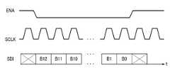
도 5는 도 4에 도시한 계조 전압 생성부의 구동 신호를 도시하는 파형도.FIG. 5 is a waveform diagram showing a drive signal of a gray voltage generator shown in FIG. 4; FIG.
<도면 부호의 설명><Description of Drawing>
Gi: 게이트선Dj: 데이터선Gi : Gate line Dj : Data line
300: 표시판400: 게이트 구동부300: display panel 400: gate driver
500: 데이터 구동부600: 신호 제어부500: data driver 600: signal controller
700: 전압 생성부800: 계조 전압 생성부700: voltage generator 800: gray voltage generator
900: 전류 감지부910: 전류 측정 회로900: current sensing unit 910: current measurement circuit
920: 아날로그-디지털 변환기920: analog to digital converter
본 발명은 표시 장치 및 그 구동 방법에 관한 것으로서, 더욱 상세하게는 유기 발광 표시 장치 및 그 구동 방법에 관한 것이다.The present invention relates to a display device and a driving method thereof, and more particularly, to an organic light emitting display device and a driving method thereof.
근래 들어 유기 발광 표시 장치는 액정 표시 장치(liquid crystal display, LCD)와 함께 평판 표시 장치로서 주목 받고 있다. 능동형(active matrix) 유기 발광 표시 장치는 유기 발광 다이오드(organic light emitting diode, OLED)와 유기 발광 다이오드에 전류를 공급해주는 구동 박막 트랜지스터(thin film transistor, TFT)를 포함한다.Recently, the organic light emitting diode display has attracted attention as a flat panel display along with a liquid crystal display (LCD). An active matrix organic light emitting display device includes an organic light emitting diode (OLED) and a driving thin film transistor (TFT) that supplies current to the organic light emitting diode.
박막 트랜지스터는 활성층(active layer)의 종류에 따라 다결정 규소(poly silicon) 박막 트랜지스터와 비정질 규소(amorphous silicon) 박막 트랜지스터 등으로 구분된다. 다결정 규소 박막 트랜지스터를 채용한 유기 발광 표시 장치는 여러 가지 장점이 있어서 널리 사용되고 있으나 박막 트랜지스터의 제조 공정이 복잡하고 균일성이 떨어진다. 반면 비정질 규소 박막 트랜지스터를 채용한 유기 발광 표시 장치는 대화면을 얻기 용이하고, 다결정 규소 박막 트랜지스터를 채용한 유기 발광 표시 장치보다 제조 공정 수효도 상대적으로 적다.The thin film transistor is classified into a polysilicon thin film transistor and an amorphous silicon thin film transistor according to the type of the active layer. The organic light emitting diode display employing the polysilicon thin film transistor has many advantages, but is widely used. However, the manufacturing process of the thin film transistor is complicated and inferior in uniformity. On the other hand, an organic light emitting diode display employing an amorphous silicon thin film transistor is easy to obtain a large screen and has a relatively smaller manufacturing process than an organic light emitting diode display employing a polysilicon thin film transistor.
한편, 구동 박막 트랜지스터의 제어 단자에는 정극성의 전압이 지속적으로 인가되며, 비정질 규소 박막 트랜지스터의 경우 이러한 지속적인 전압 인가에 따라 문턱 전압이 높아진다. 문턱 전압이 높아지면 이전과 동일한 제어 전압이 박막 트랜지스터에 인가되더라도 박막 트랜지스터가 구동하는 전류가 줄어들며 이에 따라 유기 발광 다이오드의 휘도 또한 낮아진다.On the other hand, a positive voltage is continuously applied to the control terminal of the driving thin film transistor, and in the case of the amorphous silicon thin film transistor, the threshold voltage is increased according to the continuous voltage application. When the threshold voltage is increased, even if the same control voltage is applied to the thin film transistor, the current driven by the thin film transistor is reduced, thereby lowering the luminance of the organic light emitting diode.
그뿐 아니라, 유기 발광 다이오드 자체도 시간이 흐름에 따라 성능이 나빠져서 이전과 동일한 구동 전류가 들어와도 휘도가 낮아진다.In addition, the organic light emitting diode itself deteriorates with time, and thus the luminance is lowered even when the same driving current is applied.
이러한 구동 박막 트랜지스터 및 유기 발광 다이오드의 성능 저하로 인하 휘도 하강을 보상하기 위하여 여러 가지 화소 회로가 제안되었다. 그러나 현재까지 제안된 화소 회로는 대부분 박막 트랜지스터, 축전기 및 배선 등을 다수 포함하고 있어서 화소의 개구율이 낮다.Various pixel circuits have been proposed to compensate for the lowered luminance drop due to the degradation of the driving thin film transistor and the organic light emitting diode. However, the pixel circuits proposed to date include many thin film transistors, capacitors, and wirings, so that the aperture ratio of the pixels is low.
본 발명이 이루고자 하는 기술적 과제는 유기 발광 표시 장치의 개구율을 줄이지 않고도 시간이 흐름에 따른 휘도 하강을 보상하여, 표시 장치의 수명을 연장하는 것이다.The technical problem to be achieved by the present invention is to compensate for the decrease in luminance over time without reducing the aperture ratio of the organic light emitting display device, thereby extending the life of the display device.
본 발명의 한 실시예에 따른 유기 발광 표시 장치는 행렬로 배열되어 있으며 스위칭 트랜지스터와 구동 트랜지스터를 각각 포함하는 복수의 화소, 상기 스위칭 트랜지스터에 연결되어 있으며 상기 화소에 데이터 전압을 전달하는 복수의 데이터선, 상기 구동 트랜지스터에 구동 전압을 전달하는 구동 전압선, 상기 구동 전압선에 구동 전압을 인가하는 전압 생성부, 상기 전압 생성부로부터 상기 구동 전압선으로 흐르는 구동 전류를 감지하는 전류 감지부, 상기 구동 전류의 변화량에 따라 값이 달라지는 계조 전압을 생성하는 계조 전압 생성부, 그리고 상기 계조 전압에 기초하여 입력 영상 신호를 데이터 전압으로 변환하여 상기 데이터선에 인가하는 데이터 구동부를 포함한다.The organic light emitting diode display according to the exemplary embodiment of the present invention includes a plurality of pixels arranged in a matrix, each pixel including a switching transistor and a driving transistor, and a plurality of data lines connected to the switching transistor and transferring a data voltage to the pixel. A driving voltage line transferring a driving voltage to the driving transistor, a voltage generating unit applying a driving voltage to the driving voltage line, a current sensing unit sensing a driving current flowing from the voltage generating unit to the driving voltage line, and a change amount of the driving current And a gray voltage generator for generating a gray voltage having a different value according to the first, and a data driver converting an input image signal into a data voltage based on the gray voltage and applying the gray voltage to the data line.
상기 구동 전류에 해당하는 데이터를 기준 전류에 해당하는 데이터와 비교하여 상기 구동 전류의 변화량을 산출하고, 상기 구동 전류의 변화량에 따라 상기 계조 전압 생성부를 제어하는 신호 제어부를 더 포함할 수 있다.The apparatus may further include a signal controller configured to calculate a change amount of the drive current by comparing the data corresponding to the drive current with data corresponding to a reference current, and to control the gray voltage generator according to the change amount of the drive current.
상기 신호 제어부는 상기 구동 전류를 측정할 때, 상기 기준 계조 전압의 수준을 유지하도록 상기 계조 전압 생성부를 제어할 수 있다.The signal controller may control the gray voltage generator to maintain the level of the reference gray voltage when the driving current is measured.
상기 신호 제어부는 상기 구동 전류를 측정할 때, 상기 기준 계조 전압을 초기값으로 만들도록 상기 계조 전압 생성부를 제어할 수 있다.The signal controller may control the gray voltage generator to set the reference gray voltage as an initial value when the driving current is measured.
상기 전류 감지부는 상기 구동 전류에 관한 신호를 디지털 값으로 바꾸어 상기 신호 제어부에 전달하는 아날로그-디지털 변환기를 포함할 수 있다.The current sensing unit may include an analog-to-digital converter that converts a signal related to the driving current into a digital value and transmits the signal to the signal controller.
상기 구동 전류는 상기 복수의 화소에 동일한 데이터 전압이 인가된 상태에서 측정될 수 있다.The driving current may be measured while the same data voltage is applied to the plurality of pixels.
상기 데이터 전압은 소정 계조에 대응하는 데이터 전압일 수 있다.The data voltage may be a data voltage corresponding to a predetermined gray scale.
상기 소정의 계조는 최고 계조 또는 중간 계조일 수 있다.The predetermined gray level may be the highest gray level or the middle gray level.
상기 구동 전류는 상기 유기 발광 표시 장치가 턴 온된 직후 또는 턴 오프된 직후에 측정될 수 있다.The driving current may be measured immediately after the organic light emitting diode display is turned on or immediately after it is turned off.
상기 구동 전류는 서로 다른 세가지 색상에 해당하는 입력 영상 신호 각각의 경우에 산출될 수 있다.The driving current may be calculated for each input image signal corresponding to three different colors.
상기 서로 다른 세가지 색상은 적색, 녹색 및 청색일 수 있다.The three different colors may be red, green, and blue.
상기 구동 전류의 변화량이 증가함에 따라 상기 기준 계조 전압의 값이 높아질 수 있다.As the amount of change in the driving current increases, the value of the reference gray voltage may increase.
본 발명의 다른 실시예에 따른 유기 발광 표시 장치의 구동 방법은 행렬로 배열된 복수의 화소, 상기 화소에 연결되어 있는 복수의 구동 전압선, 상기 구동 전압선에 구동 전압을 인가하는 전압 생성부를 포함하는 유기 발광 표시 장치의 구동 방법으로서, 상기 전압 생성부와 상기 구동 전압선 사이에 흐르는 구동 전류를 측정하는 단계, 상기 구동 전류와 기준 전류를 비교하여 전류 변화량을 산출하는 단계, 그리고 상기 전류 변화량에 따라 기준 계조 전압을 생성하는 단계를 포함한다.According to another aspect of the present invention, there is provided a method of driving an organic light emitting diode display, including a plurality of pixels arranged in a matrix, a plurality of driving voltage lines connected to the pixels, and a voltage generator configured to apply a driving voltage to the driving voltage lines. A driving method of a light emitting display device, the method comprising: measuring a driving current flowing between the voltage generating unit and the driving voltage line, comparing the driving current with a reference current, calculating a current change amount, and a reference gray scale according to the current change amount Generating a voltage.
상기 전류 변화량이 커질수록 상기 기준 계조 전압의 값도 높아질 수 있다.As the amount of change of current increases, the value of the reference gray voltage may also increase.
상기 구동 전류의 측정 시점은 상기 유기 발광 표시 장치가 턴 온된 직후 또는 턴 오프된 직후일 수 있다.The measurement time of the driving current may be immediately after the organic light emitting diode display is turned on or immediately after it is turned off.
상기 구동 전류는 상기 복수의 화소에 동일한 데이터 전압이 인가된 상태에서 측정될 수 있다.The driving current may be measured while the same data voltage is applied to the plurality of pixels.
상기 데이터 전압은 최고 계조 또는 중간 계조에 해당하는 데이터 전압일 수 있다.The data voltage may be a data voltage corresponding to the highest gray level or the middle gray level.
그러면 첨부한 도면을 참고로 하여 본 발명의 실시예에 대하여 본 발명이 속하는 기술 분야에서 통상의 지식을 가진 자가 용이하게 실시할 수 있도록 상세히 설명한다. 그러나 본 발명은 여러 가지 상이한 형태로 구현될 수 있으며 여기에서 설명하는 실시예에 한정되지 않는다.DETAILED DESCRIPTION Hereinafter, exemplary embodiments of the present invention will be described in detail with reference to the accompanying drawings so that those skilled in the art may easily implement the present invention. As those skilled in the art would realize, the described embodiments may be modified in various different ways, all without departing from the spirit or scope of the present invention.
도면에서 여러 층 및 영역을 명확하게 표현하기 위하여 두께를 확대하여 나타내었다. 명세서 전체를 통하여 유사한 부분에 대해서는 동일한 도면 부호를 붙였다. 층, 막, 영역, 판 등의 부분이 다른 부분 "위에" 있다고 할 때, 이는 다른 부분 "바로 위에" 있는 경우뿐 아니라 그 중간에 또 다른 부분이 있는 경우도 포함한다. 반대로 어떤 부분이 다른 부분 "바로 위에" 있다고 할 때에는 중간에 다른 부분이 없는 것을 뜻한다.In the drawings, the thickness of layers, films, panels, regions, etc., are exaggerated for clarity. Like parts are designated by like reference numerals throughout the specification. When a part of a layer, film, region, plate, etc. is said to be "on" another part, this includes not only the other part being "right over" but also another part in the middle. On the contrary, when a part is "just above" another part, there is no other part in the middle.
먼저, 도 1 및 도 2를 참고로 하여 본 발명의 한 실시예에 따른 유기 발광 표시 장치에 대하여 설명한다.First, an organic light emitting diode display according to an exemplary embodiment of the present invention will be described with reference to FIGS. 1 and 2.
도 1은 본 발명의 한 실시예에 따른 유기 발광 표시 장치의 블록도이고, 도 2는 본 발명의 한 실시예에 따른 유기 발광 표시 장치에서 한 화소의 등가 회로도이다.1 is a block diagram of an organic light emitting diode display according to an exemplary embodiment of the present invention, and FIG. 2 is an equivalent circuit diagram of one pixel in the organic light emitting diode display according to an exemplary embodiment of the present invention.
도 1에 도시한 바와 같이, 본 발명의 한 실시예에 따른 유기 발광 표시 장치는 표시판(display panel)(300), 주사 구동부(scanning driver)(400), 데이터 구동부(data driver)(500), 전압 생성부(voltage generator)(700), 계조 전압 생성부(gray voltage generator)(800), 전류 감지부(current sensing unit)(900) 및 신호 제어부(signal controller)(600)를 포함한다.As illustrated in FIG. 1, an organic light emitting diode display according to an exemplary embodiment of the present invention may include a
표시판(300)은 복수의 신호선(G1-Gn, D1-Dm), 구동 전압선(driving voltage line)(VL), 그리고 이들에 연결되어 있으며 대략 행렬(matrix)의 형태로 배열된 복 수의 화소(pixel)(PX)를 포함한다.The
신호선은 주사 신호를 전달하는 복수의 주사 신호선(scanning line)(G1-Gn) 및 데이터 전압을 전달하는 데이터선(data line)(D1-Dm)을 포함한다. 주사 신호선(G1-Gn)은 대략 행 방향으로 뻗어 있으며 서로가 거의 평행하고 데이터선(D1-Dm)은 대략 열 방향으로 뻗어 있으며 서로가 거의 평행하다.The signal line includes a plurality of scanning lines G1 -Gn for transmitting a scan signal and data lines D1 -Dm for transmitting a data voltage. The scan signal lines G1 -Gn extend substantially in the row direction and are substantially parallel to each other, and the data lines D1 -Dm extend substantially in the column direction and are substantially parallel to each other.
구동 전압선(VL)은 구동 전압(Vdd)을 전달하며, 줄기선(VLm)과 이로부터 갈라진 복수의 가지선(VLb)을 포함한다. 줄기선(VLm)은 대략 행 방향으로 뻗어 있으며, 가지선(VLb)은 대략 열 방향으로 뻗어 있다. 그러나 줄기선(VLm)이 열 방향으로, 가지선(VLb)이 행 방향으로 뻗을 수도 있으며, 그 외에도 여러 가지 형태로 구현될 수 있다.The driving voltage line VL transfers the driving voltage Vdd and includes a stem line VLm and a plurality of branch lines VLb split therefrom. Stem line VLm extends in a substantially row direction, and branch line VLb extends in a substantially column direction. However, the stem line VLm may extend in the column direction, the branch line VLb may extend in the row direction, and may be embodied in various forms.
도 2에 도시한 바와 같이, 각 화소(PX), 예를 들면 i 번째 주사 신호선(Gi)과 j번째 데이터선(Dj)에 연결되어 있는 화소(PX)는 유기 발광 소자(organic light emitting element)(LD), 구동 트랜지스터(driving transistor)(Qd), 유지 축전기(storage capacitor)(Cst) 및 스위칭 트랜지스터(switching transistor)(Qs)를 포함한다.As illustrated in FIG. 2, each pixel PX, for example, the pixel PX connected to the i-th scan signal line Gi and the j-th data line Dj is an organic light emitting device. element LD, a driving transistor Qd, a storage capacitor Cst, and a switching transistor Qs.
스위칭 트랜지스터(Qs)는 제어 단자(control terminal), 입력 단자(input terminal) 및 출력 단자(output terminal)를 가지는데, 제어 단자는 주사 신호선(Gi)과 연결되어 있고, 입력 단자는 데이터선(Dj)과 연결되어 있으며, 출력 단자 는 구동 트랜지스터(Qd)와 연결되어 있다. 스위칭 트랜지스터(Qs)는 주사 신호선(Gi)에 인가되는 주사 신호에 응답하여 데이터선(Dj)에 인가되는 데이터 전압을 전달한다.The switching transistor Qs has a control terminal, an input terminal, and an output terminal. The control terminal is connected to the scan signal line Gi , and the input terminal is a data line ( Dj ) and the output terminal is connected to the driving transistor Qd. A switching transistor (Qs) transfers the data voltage to be applied to the response to the scanning signals applied to scanning signal lines (Gi) the data lines (Dj).
구동 트랜지스터(Qd) 또한 제어 단자, 입력 단자 및 출력 단자를 가지는데, 제어 단자는 스위칭 트랜지스터(Qs)와 연결되어 있고, 입력 단자는 구동 전압선(VL)의 가지선(VLb)과 연결되어 있으며, 출력 단자는 유기 발광 소자(LD)와 연결되어 있다. 구동 트랜지스터(Qd)는 제어 단자와 출력 단자 사이에 걸리는 전압에 따라 그 크기가 달라지는 출력 전류(ILD)를 흘린다.The driving transistor Qd also has a control terminal, an input terminal, and an output terminal. The control terminal is connected to the switching transistor Qs, and the input terminal is connected to the branch line VLb of the driving voltage line VL. The output terminal is connected to the organic light emitting element LD. The driving transistor Qd flows an output current ILD whose magnitude varies depending on the voltage applied between the control terminal and the output terminal.
유지 축전기(Cst)는 구동 트랜지스터(Qd)의 제어 단자와 입력 단자 사이에 연결되어 있다. 유지 축전기(Cst)는 구동 트랜지스터(Qd)의 제어 단자에 인가되는 데이터 전압을 충전하고 스위칭 트랜지스터(Qs)가 턴 오프된 뒤에도 이를 유지한다.The storage capacitor Cst is connected between the control terminal and the input terminal of the driving transistor Qd. The storage capacitor Cst charges the data voltage applied to the control terminal of the driving transistor Qd and maintains it even after the switching transistor Qs is turned off.
유기 발광 소자(LD)는 유기 발광 다이오드(OLED)로서 구동 트랜지스터(Qd)의 출력 단자에 연결되어 있는 애노드(anode)와 공통 전압(Vcom)에 연결되어 있는 캐소드(cathode)를 가진다. 애노드는 두 개의 주사 신호선(G1-Gn)과 두 개의 데이터선(D1-Dm)으로 구획되는 영역 내에 대략 위치하는 화소 전극(pixel electrode)(도시하지 않음)일 수 있으며, 캐소드는 표시판(300)의 전면(全面)에 형성되어 있는 공통 전극(common electrode)(도시하지 않음)의 일부일 수 있다. 유기 발광 소 자(LD)는 구동 트랜지스터(Qd)의 출력 전류(ILD)에 따라 세기를 달리하여 발광함으로써 영상을 표시한다.The organic light emitting element LD is an organic light emitting diode OLED and has an anode connected to an output terminal of the driving transistor Qd and a cathode connected to a common voltage Vcom. The anode may be a pixel electrode (not shown) located approximately in an area partitioned by two scan signal lines G1 -Gn and two data lines D1 -Dm , and the cathode is The
유기 발광 소자(LD)는 기본색(primary color) 중 하나의 빛을 내거나, 기본색과 백색 중 하나의 빛을 낼 수 있다. 기본색의 예로는 적색, 녹색, 청색의 삼원색을 들 수 있으며 이들 삼원색의 공간적 합으로 원하는 색상을 표시한다. 이와는 달리, 모든 화소(PX)의 유기 발광 소자(LD)가 백색의 빛을 낼 수 있으며, 일부 화소(PX)는 유기 발광 소자(LD)에서 나오는 백색광을 기본색광 중 어느 하나로 바꿔주는 색필터(도시하지 않음)를 더 포함할 수 있다.The organic light emitting element LD may emit light of one of primary colors or one of primary colors and white. Examples of the primary colors include three primary colors of red, green, and blue, and the desired color is represented by a spatial sum of these three primary colors. On the contrary, the organic light emitting element LD of all the pixels PX may emit white light, and some pixels PX convert the white light emitted from the organic light emitting element LD into one of the primary color light. Not shown).
스위칭 트랜지스터(Qs) 및 구동 트랜지스터(Qd)는 비정질 규소 또는 다결정 규소로 만들어진 n-채널 전계 효과 트랜지스터(field effect transistor, FET)이다. 그러나 스위칭 트랜지스터(Qs)와 구동 트랜지스터(Qd) 중 적어도 하나는 p-채널 전계 효과 트랜지스터일 수 있다. 또한, 트랜지스터(Qs, Qd), 축전기(Cst) 및 유기 발광 소자(LD)의 연결 관계가 바뀔 수 있다.The switching transistor Qs and the driving transistor Qd are n-channel field effect transistors (FETs) made of amorphous silicon or polycrystalline silicon. However, at least one of the switching transistor Qs and the driving transistor Qd may be a p-channel field effect transistor. In addition, the connection relationship between the transistors Qs and Qd, the capacitor Cst, and the organic light emitting element LD may be changed.
다시 도 1을 참조하면, 계조 전압 생성부(800)는 화소(PX)의 휘도와 관련된 복수의 기준 계조 전압을 생성한다. 기준 계조 전압의 수효는 전체 계조의 수효보다 작고, 그 전압값은 시간에 따라 변화하며 신호 제어부(600)의 제어에 따라 표시 장치의 휘도 감소에 대한 보상값이 반영되어 있다.Referring back to FIG. 1, the
주사 구동부(400)는 표시판(300)의 주사 신호선(G1-Gn)에 연결되어 스위칭 트랜지스터(Qs)를 턴온시킬 수 있는 고전압(Von)과 턴 오프시킬 수 있는 저전 압(Voff)의 조합으로 이루어진 주사 신호를 주사 신호선(G1-Gn)에 인가한다.The
데이터 구동부(500)는 표시판(300)의 데이터선(D1-Dm)에 연결되어 있으며, 계조 전압 생성부(800)로부터 받은 기준 계조 전압을 분압하여 데이터 전압을 생성하고 이를 데이터선(D1-Dm)에 인가한다.The
전압 생성부(700)는 표시판(300)의 구동 전압선(VL)과 연결되어 있으며, 구동 전압(Vdd)을 생성하여 구동 전압선(VL)에 인가한다. 또한 전압 생성부(700)는 표시판(300)에 공통 전압(Vcom)을 인가한다.The
전류 감지부(900)는 전압 생성부(700)와 구동 전압선(VL) 사이에 흐르는 구동 전류(Idd)를 감지하며, 전류 측정 회로(current measurement circuit)(910) 및 아날로그-디지털 변환기(analog-to-digital converter)(920)를 포함한다.The
전류 측정 회로(910)는 전압 생성부(700)로부터 구동 전압선(VL)으로 흐르는 구동 전류(Idd)를 측정하여 이에 대응하는 아날로그 전류 측정 신호(AI)를 생성한다. 전류 측정 회로(910)가 생성한 아날로그 전류 측정 신호(AI)는 전압 신호일 수 있으며, 전류 측정 회로(910)는 구동 전압선(VL)과 직접 연결되어 구동 전압선(VL) 자체에 흐르는 전류를 측정할 수도 있다.The
아날로그-디지털 변환기(ADC)(920)는 전류 측정 회로(910)로부터 받은 아날로그 전류 측정 신호(AI)를 디지털 전류 측정 신호(DI)로 변환한다.The analog-to-digital converter (ADC) 920 converts the analog current measurement signal AI received from the
신호 제어부(600)는 주사 구동부(400), 데이터 구동부(500), 계조 전압 생성부(800) 및 전류 감지부(900) 등을 제어한다.The
이러한 구동 장치(400, 500, 600, 700, 800, 900) 각각은 신호선(G1-Gn, D1-Dm) 및 박막 트랜지스터(Q) 스위칭 소자(Q) 따위와 함께 액정 표시판(300)에 집적될 수도 있다. 이와는 달리 이들 구동 장치(400, 500, 600, 700, 800, 900)가 적어도 하나의 집적 회로 칩의 형태로 표시판(300) 위에 직접 장착되거나, 가요성 인쇄 회로막(flexible printed circuit film)(도시하지 않음) 위에 장착되어 TCP(tape carrier package)의 형태로 표시판(300)에 부착되거나, 별도의 인쇄 회로 기판(printed circuit board)(도시하지 않음) 위에 장착될 수도 있다. 또한, 구동 장치(400, 500, 600, 700, 800, 900)는 단일 칩으로 집적될 수 있으며, 이 경우 이들 중 적어도 하나 또는 이들을 이루는 적어도 하나의 회로 소자가 단일 칩 바깥에 있을 수 있다.Each of the driving
그러면 이러한 유기 발광 표시 장치의 동작에 대하여 상세하게 설명한다.Next, the operation of the organic light emitting diode display will be described in detail.
신호 제어부(600)는 외부의 그래픽 제어기(도시하지 않음)로부터 입력 영상 신호(R, G, B) 및 이의 표시를 제어하는 입력 제어 신호를 수신한다. 입력 영상 신호(R, G, B)는 각 화소(PX)의 휘도(luminance) 정보를 담고 있으며 휘도는 정해진 수효, 예를 들면 1024(=210), 256(=28) 또는 64(=26) 개의 계조(gray)를 가지고 있다. 입력 제어 신호의 예로는 수직 동기 신호(Vsync)와 수평 동기 신호(Hsync), 메인 클록 신호(MCLK), 데이터 인에이블 신호(DE) 등이 있다.The
신호 제어부(600)는 입력 영상 신호(R, G, B)와 입력 제어 신호를 기초로 입력 영상 신호(R, G, B)를 표시판(300)의 동작 조건에 맞게 적절히 처리하여 출력 영상 신호(DAT)를 생성하고 주사 제어 신호(CONT1), 데이터 제어 신호(CONT2), 계조 전압 제어 신호(CONT3) 및 전류 감지 제어 신호(CONT4) 등을 생성한다. 신호 제어부(600)는 주사 제어 신호(CONT1)를 게이트 구동부(400)로, 계조 전압 제어 신호(CONT3)를 계조 전압 생성부(800)로, 전류 감지 제어 신호(CONT4)를 전류 감지부(900)로 각각 내보내고, 데이터 제어 신호(CONT2)와 출력 영상 신호(DAT)를 데이터 구동부(500)로 내보낸다.The
주사 제어 신호(CONT1)는 고전압(Von)의 주사 시작을 지시하는 주사 시작 신호(STV)와 고전압(Von)의 출력 주기를 제어하는 적어도 하나의 클록 신호를 포함한다. 주사 제어 신호(CONT1)는 또한 게이트 온 전압(Von)의 지속 시간을 한정하는 출력 인에이블 신호(OE)를 더 포함할 수 있다.The scan control signal CONT1 includes a scan start signal STV for instructing the scan start of the high voltage Von and at least one clock signal for controlling the output period of the high voltage Von. The scan control signal CONT1 may also further include an output enable signal OE that defines the duration of the gate-on voltage Von.
데이터 제어 신호(CONT2)는 한 행의 화소(PX)에 대한 디지털 영상 신호(DAT)의 전송 시작을 알리는 수평 동기 시작 신호(STH)와 데이터선(D1-Dm)에 아날로그 데이터 전압을 인가하라는 로드 신호(LOAD) 및 데이터 클록 신호(HCLK)를 포함한다.The data control signal CONT2 applies an analog data voltage to the horizontal synchronizing start signal STH and the data lines D1 -Dm indicating the start of transmission of the digital image signal DAT for one row of pixels PX. Includes a load signal LOAD and a data clock signal HCLK.
계조 전압 제어 신호(CONT3)는 기준 계조 전압 생성에 필요한 정보를 주는 디지털 신호인 감마 데이터(gamma data)를 포함한다.The gray voltage control signal CONT3 includes gamma data, which is a digital signal that provides information necessary for generating a reference gray voltage.
계조 전압 생성부(800)는 신호 제어부(600)로부터의 계조 전압 제어 신호(CONT3)에 따라 기준 계조 전압을 생성하여 이를 데이터 구동부(500)에 제공한다.The
신호 제어부(600)로부터의 데이터 제어 신호(CONT2)에 따라 데이터 구동 부(500)는 한 행의 화소에 대한 출력 영상 데이터(DAT)를 수신하고, 기준 계조 전압을 분압하여 출력 영상 데이터(DAT)에 대응하는 아날로그 데이터 전압을 생성한 후 이를 해당 데이터선(D1-Dm)에 인가한다.In response to the data control signal CONT2 from the
주사 구동부(400)는 신호 제어부(600)로부터의 주사 제어 신호(CONT1)에 따라 주사 신호선(G1-Gn)에 인가되는 주사 신호를 고전압(Von)으로 변환한다. 그러면, 이 주사 신호선(G1-Gn)에 연결된 스위칭 트랜지스터(Qs)가 턴 온되어 데이터선(D1-Dm)에 인가된 데이터 전압을 해당 화소(PX)의 구동 트랜지스터(Qd)의 제어 단자에 인가한다.The
구동 트랜지스터(Qd)에 인가된 데이터 전압은 축전기(Cst)에 충전되고 스위칭 트랜지스터(Qs)가 오프되더라도 충전된 전압은 유지된다. 데이터 전압이 인가된 구동 트랜지스터(Qd)는 턴온되어, 데이터 전압에 의존하는 값을 가지는 출력 전류(ILD)를 출력한다. 그리고 유기 발광 소자(LD)는 구동 전류(ILD)의 크기에 따라 변하는 세기로 발광하며 이에 따라 해당 화소(PX)는 영상을 표시한다.The data voltage applied to the driving transistor Qd is charged in the capacitor Cst and the charged voltage is maintained even when the switching transistor Qs is turned off. The driving transistor Qd to which the data voltage is applied is turned on to output an output current ILD having a value dependent on the data voltage. In addition, the organic light emitting element LD emits light having an intensity varying according to the size of the driving current ILD . Accordingly, the corresponding pixel PX displays an image.
1 수평 주기(또는 "1H")[수평 동기 신호(Hsync), 데이터 인에이블 신호(DE)의 한 주기]가 지나면 데이터 구동부(500)와 주사 구동부(400)는 다음 행의 화소(PX)에 대하여 동일한 동작을 반복한다. 이러한 방식으로, 한 프레임(frame) 동안 모든 주사 신호선(G1-Gn)에 대하여 차례로 주사 신호를 인가하여, 모든 화소(PX)에 데이터 전압을 인가한다. 한 프레임이 끝나면 다음 프레임이 시작되고 다음 프 레임에서도 동일한 동작을 반복한다.After one horizontal period (or "1H") (one period of the horizontal synchronization signal Hsync and the data enable signal DE) has passed, the
한편, 구동 트랜지스터(Qd)의 출력 전류(ILD)는 구동 전압선(VL)의 가지선(VLb)으로부터 공통 전압(Vcom) 쪽으로 흐르며, 이에 따라 전압 생성부(900)로부터 구동 전압선(VL)으로 흐르는 전류(Idd)(이하 구동 전류라 한다.)가 생긴다. 구동 트랜지스터(Qd)의 출력 전류(ILD)는 시간이 흐름에 따른 구동 트랜지스터(Qd)의 성능 저하로 인하여 점점 줄어들고 이에 따라 구동 전류(ILD) 또한 줄어든다. 따라서 구동 전류(ILD)의 변화량을 알면 구동 트랜지스터(Qd)의 열화 정도를 알 수 있다.On the other hand, the output current ILD of the driving transistor Qd flows from the branch line VLb of the driving voltage line VL toward the common voltage Vcom, and thus from the
본 실시예에서는 구동 전류(ILD)를 측정하고 이에 기초하여 계조 전압 생성부(800)가 생성하는 기준 계조 전압의 값을 보정함으로써 화소(PX)에 인가되는 데이터 전압의 크기를 바꿔준다. 이와 같이 하면, 동일한 입력 영상 신호(R, G, B)에 대하여 구동 트랜지스터(Qd)의 출력 전류(ILD)가 일정하게 되고 유기 발광 소자(LD)의 휘도 또한 일정해진다.In the present exemplary embodiment, the magnitude of the data voltage applied to the pixel PX is changed by measuring the driving current ILD and correcting the value of the reference gray voltage generated by the
이러한 기준 계조 전압의 값 보정 과정에 대하여 상세하게 설명한다.The process of correcting the value of the reference gray voltage will be described in detail.
먼저, 전류 측정 회로(910)는 전압 생성부(900)과 구동 전압선(VL) 사이에 흐르는 구동 전류(Idd)를 측정한다.First, the
구동 전류(Idd)의 측정은 유기 발광 표시 장치를 사용한 지 일정한 시간이 흐른 후부터 시작할 수 있으며, 측정 시점은 사용자가 유기 발광 표시 장치를 켠 직후 또는 끈 직후일 수 있다. 또한 구동 전류(ILD)의 측정은 모든 화소(PX)에 동일한 데이터 전압이 인가된 상태에서 이루어질 수 있다. 이 때의 데이터 전압은 소정 계조, 이를테면 최고 계조 또는 중간 계조에 대응하는 데이터 전압일 수 있다. 모든 화소(PX)에 동일한 데이터 전압을 인가하면 비정상적인 영상이 표시되지만, 사용자가 유기 발광 표시 장치를 켜거나 끈 직후에는 유기 발광 표시 장치가 정상적인 영상인 영상을 표시하는 것이 아니므로 표시에 지장을 주지 않는다.The measurement of the driving current Idd may begin after a certain time has passed since the organic light emitting diode display was used, and the measurement time point may be immediately after the user turns on or immediately turns off the organic light emitting diode display. In addition, the measurement of the driving current ILD may be performed while the same data voltage is applied to all the pixels PX. In this case, the data voltage may be a data voltage corresponding to a predetermined gray level, for example, a highest gray level or a middle gray level. When the same data voltage is applied to all the pixels PX, an abnormal image is displayed. However, immediately after the user turns on or turns off the organic light emitting diode display, the organic light emitting diode display does not display a normal image. Do not.
구동 전류(ILD)의 측정을 위한 이러한 동작은 신호 제어부(600)에서 수행할 수 있다. 예를 들어 신호 제어부(600)는 사용자가 유기 발광 표시 장치를 켜는/끄는 스위치 온/오프 신호가 들어오면 외부에서 들어오는 입력 영상 신호(R, G, B)를 차단하고 앞서 설명한 소정 계조를 가지는 출력 영상 신호(DAT)를 데이터 구동부(500)에 전송한다. 이와 동시에 신호 제어부(600)는 전류 감지 제어 신호(CONT4)를 통하여 전류 감지부(900)가 구동 전류(ILD)를 감지하도록 한다.This operation for measuring the driving current ILD may be performed by the
전류 측정 회로(910)는 측정한 구동 전류(Idd)에 대응하는 아날로그 전류 측정 신호(AI)를 생성하여 아날로그-디지털 변환기(920)로 출력한다. 그러면 아날로그-디지털 변환기(920)는 아날로그 전류 측정 신호(AI)를 디지털 전류 측정 신호(DI)로 변환하여 신호 제어부(600)에 출력한다.The
신호 제어부(600)는 아날로그-디지털 변환기(920)로부터 받은 디지털 전류 측정 신호(DI)를 미리 기억되어 있는 기준 데이터와 비교하고 그 비교 결과에 따라 계조 전압 제어 신호(CONT3)인 감마 데이터를 바꾼다. 예를 들면 신호 제어 부(600)는 디지털 전류 측정 신호(DI)와 기준 데이터의 차이를 구하고 이에 따라 감마 데이터를 바꿀 수 있다.The
여기에서 기준 데이터는 예를 들어 유기 발광 표시 장치를 처음 사용할 때 구동 전류(Idd)를 측정하고 이를 디지털 전류 측정 신호(DI)로 변환한 디지털 값일 수 있다. 이와는 달리 유기 발광 표시 장치의 제품 특성에 따라 제조 과정에서 미리 정한 값일 수도 있다.The reference data may be, for example, a digital value obtained by measuring the driving current Idd and converting the driving current Idd into a digital current measurement signal DI when the organic light emitting diode display is first used. Alternatively, the value may be predetermined in the manufacturing process according to the product characteristics of the OLED display.
계조 전압 생성부(800)는 신호 제어부(600)로부터의 감마 데이터에 따라 데이터 구동부(500)에 제공하는 기준 계조 전압의 값을 바꾸며, 이에 따라 데이터 구동부(500)가 생성하는 데이터 전압 또한 그 값이 달라진다.The
그러면 도 3을 참고하여 본 발명의 한 실시예에 따른 유기 발광 표시 장치의 기준 계조 전압의 한 예에 대하여 상세하게 설명한다.Next, an example of the reference gray voltage of the organic light emitting diode display according to the exemplary embodiment of the present invention will be described in detail with reference to FIG. 3.
도 3은 본 발명의 한 실시예에 따른 유기 발광 표시 장치의 계조 전압의 예를 계조의 함수로 도시한 그래프이다.3 is a graph showing an example of a gray voltage of an organic light emitting diode display according to an exemplary embodiment of the present invention as a function of gray scale.
도 3을 참고하면, x 축은 첫 번째 계조에서부터 64 번째 계조까지 총 64 계조를 표시하며 y 축은 0과 1 사이로 규격화한(normalized) 계조 전압이다. 본 발명의 실시예에 따른 계조 전압 생성부(800)가 생성하는 기준 계조 전압은 이중 몇 개의 계조에 대한 계조 전압일 수 있다.Referring to FIG. 3, the x axis represents a total of 64 gray levels from the first gray level to the 64th gray level, and the y axis is a gray voltage normalized between 0 and 1. The reference gray voltage generated by the
유기 발광 표시 장치를 처음 사용할 때에는 70% 곡선을 따라 계조 전압을 값을 정할 수 있다. 이 곡선에 따르면 최대 계조인 64 번째 계조에서 기준 계조 전압이 0.7이다.When the organic light emitting diode display is used for the first time, a gray voltage may be determined along a 70% curve. According to this curve, the reference gray voltage is 0.7 at the 64th gray scale, which is the maximum gray scale.
유기 발광 표시 장치를 사용한 기간이 늘어날수록 구동 전류(ILD)가 점점 떨어지므로 기준 계조 전압의 수준은 점점 높아져서, 80% 곡선, 90% 곡선, 결국은 100% 곡선에 이르게 된다.As the duration of using the organic light emitting diode display device increases, the driving current ILD gradually decreases, and thus the level of the reference gray voltage is gradually increased to reach an 80% curve, a 90% curve, and eventually a 100% curve.
이와 같이 기준 계조 전압의 수준이 높아지면 동일한 계조에 대한 데이터 전압의 수준도 높아진다. 이때, 동일한 계조에 대해서 동일한 구동 전류(Idd)가 흐르도록 기준 계조 전압의 수준을 조절해주면, 동일한 계조에 대해서 동일한 휘도를 유지할 수 있다.As the level of the reference gray voltage increases, the level of data voltages for the same gray level also increases. In this case, if the level of the reference gray voltage is adjusted such that the same driving current Idd flows for the same gray level, the same brightness may be maintained for the same gray level.
예를 들어, 구동 전류(Idd)를 측정할 때 신호 제어부(600)는 계조 전압 생성부(800)를 제어하여 기준 계조 전압을 모두 초기값으로 만들 수 있다. 그런 상태에서 신호 제어부(600)는 앞서 설명한 소정 계조의 영상 신호를 데이터 구동부(500)로 보내어 화소(PX)들을 발광시켜 구동 전류(Idd)를 측정한다. 그러면, 디지털 전류 측정 신호(DI)와 기준 데이터의 차이는 구동 트랜지스터(Qd)의 절대적인 성능 저하 정도를 반영한 값이 된다. 따라서, 신호 제어부(600)가 측정 신호(DI)와 기준 데이터의 차이에 해당하는 감마 데이터를 룩업 테이블(도시하지 않음) 등에서 찾아 계조 전압 생성부(900)에 보냄으로써 기준 계조 전압을 보정할 수 있다.For example, when measuring the driving current Idd, the
이와는 달리, 신호 제어부(600)는 구동 전류(Idd)를 측정할 때 계조 전압 생성부(800)가 생성하는 기준 계조 전압의 수준을 그대로 유지하도록 할 수 있다. 예를 들어 기준 계조 전압이 그 전에 이미 보정이 되어 있는 상태라도 그 상태를 그대로 유지하는 것이다. 그러면, 각 화소(PX)에 인가되는 데이터 전압도 어느 정 도 보정된 값이 될 것이고, 디지털 전류 측정 신호(DI)와 기준 데이터의 차이는 구동 트랜지스터(Qd)의 절대적인 성능 저하를 반영하는 것이 아니라 이전에 보정한 상태를 기준으로 하여 구동 트랜지스터(Qd)의 성능 저하가 어느 정도 있었는지를 반영한다. 이와 같은 경우에는 디지털 전류 측정 신호(DI)와 기준 데이터의 차이가 없어질 때까지 기준 계조 전압을 계속 높여주면 된다. 이제 도 3 및 도 4를 참고하여 본 발명의 한 실시예에 따른 유기 발광 표시 장치의 계조 전압 생성부의 한 예에 대하여 상세하게 설명한다.In contrast, the
도 3은 본 발명의 한 실시예에 따른 액정 표시 장치 중 계조 전압 생성부가 구현된 집적 회로 칩의 한 예를 도시하는 도면이고, 도 4는 도 3의 계조 전압 생성부에 사용되는 신호의 파형도이다.3 is a diagram illustrating an integrated circuit chip in which a gray voltage generator is implemented in a liquid crystal display according to an exemplary embodiment of the present invention, and FIG. 4 is a waveform diagram of a signal used in the gray voltage generator of FIG. 3. to be.
도 3을 참고하면, 본 발명의 한 실시예에 따른 계조 전압 생성부(800) 칩은 클록 신호가 입력되는 직렬 클록 단자(SCLK), 기준 전압 입력 단자(REFH, REFL), 접지 단자(GND), 직렬 데이터 입력 신호가 입력되는 직렬 데이터 입력 단자(SDI), 인에이블 신호가 입력되는 인에이블 단자(ENA), 그리고 8개의 기준 계조 전압 출력 단자(OUTA, OUTB, OUTC, OUTD, OUTE, OUTF, OUTG, OUTH) 등을 포함한다.Referring to FIG. 3, a
기준 전압 입력 단자(REFH, REFL)에는 접지 전압과 더불어 기준 계조 전압을 만드는 기준이 되는 기준 전압(VREFH, VREFL)이 인가되며, 기준 전압(VREFH, VREFL)은 상대적으로 높은 상위 기준 전압(VREFH)과 상대적으로 낮은 하위 기준 전압(VREFL)의 쌍으로 이루어져 있다.The reference voltage input terminal (REFH, REFL) there is the applied reference voltage (VREFH, VREFL) serving as a reference to create a reference gradation voltage with the ground voltage, the reference voltage (VREFH, VREFL) is relatively high the upper reference It consists of a pair of voltage VREFH and a relatively low lower reference voltage VREFL .
직렬 데이터 입력 신호(SDI)는 기준 계조 전압을 생성하는 정보를 담은 데이터로서, 일반적으로 신호 제어부(600)로부터 공급받으며, 기준 계조 전압의 출력 단자를 정하는 3 비트와 기준 계조 전압의 수치를 정하는 10 비트를 포함할 수 있다. 이 밖에도 계조 전압 생성부(800)의 동작을 제어하는 디지털 신호를 더 포함할 수도 있다.The serial data input signal SDI is data containing information for generating a reference gray voltage. The serial data input signal SDI is generally supplied from the
다음 표 1은 도 3의 계조 전압 생성부의 동작을 설명하기 위한 표이다. 표 1을 도 3 및 도 4와 함께 설명한다.Table 1 below is a table for describing the operation of the gray voltage generator of FIG. 3. Table 1 is described with FIG. 3 and FIG.

인에이블 신호(ENA)가 로우 레벨인 구간 동안이 직렬 데이터 입력 신호(SDI)의 유효 구간이 된다.A period during which the enable signal ENA is at a low level becomes a valid period of the serial data input signal SDI.
직렬 데이터 입력 신호(SDI)의 12 번째 비트, 11 번째 비트 및 10 번째 비트(B12, B11, B10)는 도 6에서 A2, A1, A0로 표현되어 있으며, 기준 계조 전압의 출력 단자를 결정한다. 예를 들어, 도 6과 같이 A2, A1, A0이 000이면 기준 계조 전압의 출력 단자는 첫 번째 출력 단자(OUTA)로 지정되고, 011이면 세 번째 출력 단자(OUTC)로 지정되고, 111이면 여덟 번째 출력 단자(OUTH)로 지정된다.The 12th, 11th, and 10th bits B12, B11, and B10 of the serial data input signal SDI are represented by A2, A1, and A0 in FIG. 6 and determine an output terminal of the reference gray voltage. For example, as shown in FIG. 6, when A2, A1, and A0 are 000, the output terminal of the reference gray voltage is designated as the first output terminal OUTA, if it is 011, it is designated as the third output terminal OUTC, and if it is 111, eight Output terminal OUTH.
직렬 데이터 입력 신호(SDI)의 9 번째 비트 내지 0 번째 비트(B9~B0)는 도 6에서 D9, D8, D7, D6, D5, D4, D3, D2, D1 및 D0으로 표시되어 있으며, 이는 출력되는 기준 계조 전압의 값을 결정하는 이진 감마 데이터(GAMMA DATA)를 나타낸다. 이진 감마 데이터를 십진수로 고치면, 예를 들어, 0000000000은 0, 1111111111은 1023, 1000000000은 512, 1000000001은 513, 0000011111은 31이다.The 9th to 0th bits B9 to B0 of the serial data input signal SDI are denoted as D9, D8, D7, D6, D5, D4, D3, D2, D1 and D0 in FIG. Binary gamma data (GAMMA DATA) for determining the value of the reference gray scale voltage to be shown. For example, 0000000000 is 0, 1111111111 is 1023, 1000000000 is 512, 1000000001 is 513, and 0000011111 is 31.
계조 전압 생성부(800)는 감마 데이터(GAMMA DATA)를 다음의 수학식 1에 넣어 기준 계조 전압을 계산한 후, 해당 출력 단자(OUTA, OUTB, OUTC, OUTD, OUTE, OUTF, OUTG, OUTH)를 통하여 출력한다.The

여기서 VOUT은 기준 계조 전압 출력 단자(OUTA, OUTB, OUTC, OUTD, OUTE, OUTF, OUTG, OUTH)로 출력되는 기준 계조 전압이다.Here, VOUT is a reference gray voltage output to the reference gray voltage output terminals OUTA, OUTB, OUTC, OUTD, OUTE, OUTF, OUTG, and OUTH.
본 발명에 따르면, 유기 발광 표시 장치의 개구율을 감소하지 않고 시간에 따른 휘도 감소를 보상하여, 표시 장치의 수명을 연장한다.According to the present invention, the luminance decreases with time without compromising the aperture ratio of the organic light emitting diode display, thereby extending the life of the display apparatus.
Claims (17)
Translated fromKoreanPriority Applications (2)
| Application Number | Priority Date | Filing Date | Title |
|---|---|---|---|
| KR1020060071315AKR20080010796A (en) | 2006-07-28 | 2006-07-28 | OLED display and driving method thereof |
| US11/770,512US20080024526A1 (en) | 2006-07-28 | 2007-06-28 | Organic light emitting diode display and driving method thereof |
Applications Claiming Priority (1)
| Application Number | Priority Date | Filing Date | Title |
|---|---|---|---|
| KR1020060071315AKR20080010796A (en) | 2006-07-28 | 2006-07-28 | OLED display and driving method thereof |
Publications (1)
| Publication Number | Publication Date |
|---|---|
| KR20080010796Atrue KR20080010796A (en) | 2008-01-31 |
Family
ID=38985729
Family Applications (1)
| Application Number | Title | Priority Date | Filing Date |
|---|---|---|---|
| KR1020060071315ACeasedKR20080010796A (en) | 2006-07-28 | 2006-07-28 | OLED display and driving method thereof |
Country Status (2)
| Country | Link |
|---|---|
| US (1) | US20080024526A1 (en) |
| KR (1) | KR20080010796A (en) |
Cited By (2)
| Publication number | Priority date | Publication date | Assignee | Title |
|---|---|---|---|---|
| KR101101594B1 (en)* | 2010-08-20 | 2012-01-02 | 한국과학기술원 | Organic light emitting diode driving device |
| KR20140140964A (en)* | 2013-05-30 | 2014-12-10 | 삼성디스플레이 주식회사 | Display device and protecting method of the same |
Families Citing this family (16)
| Publication number | Priority date | Publication date | Assignee | Title |
|---|---|---|---|---|
| KR100962916B1 (en)* | 2008-08-06 | 2010-06-10 | 삼성모바일디스플레이주식회사 | Driver IC and organic light emitting display device using the same |
| JP2010049523A (en)* | 2008-08-22 | 2010-03-04 | Mitsubishi Electric Corp | Constant current switching power supply device, method of driving the same, light source drive device, method of driving the same, and image display device |
| JP5531496B2 (en)* | 2009-08-18 | 2014-06-25 | セイコーエプソン株式会社 | Image processing apparatus, display system, electronic apparatus, and image processing method |
| JP5471165B2 (en)* | 2009-08-26 | 2014-04-16 | セイコーエプソン株式会社 | Image processing apparatus, display system, electronic apparatus, and image processing method |
| JP5577812B2 (en)* | 2010-04-15 | 2014-08-27 | セイコーエプソン株式会社 | Image processing apparatus, display system, electronic apparatus, and image processing method |
| KR101990975B1 (en) | 2012-04-13 | 2019-06-19 | 삼성전자 주식회사 | Gradation voltage generator and display driving apparatus |
| KR102033374B1 (en)* | 2012-12-24 | 2019-10-18 | 엘지디스플레이 주식회사 | Organic light emitting display device and method for driving the same |
| KR102101182B1 (en)* | 2013-12-23 | 2020-04-16 | 엘지디스플레이 주식회사 | Organic light emitting display device |
| CN104036721B (en)* | 2014-05-15 | 2017-01-18 | 京东方科技集团股份有限公司 | Organic-light-emitting-diode display panel, and driving method and display device thereof |
| KR102306070B1 (en)* | 2015-04-06 | 2021-09-29 | 삼성디스플레이 주식회사 | Organic light emitting display device and mtehod of driving the same |
| KR102422053B1 (en)* | 2015-04-17 | 2022-07-19 | 삼성디스플레이 주식회사 | Data compensation device and display device including the same |
| KR102419876B1 (en)* | 2015-08-21 | 2022-07-12 | 삼성디스플레이 주식회사 | Method of compensatting degradation and display device performing the same |
| US10593243B2 (en)* | 2018-05-07 | 2020-03-17 | Novatek Microelectronics Corp. | Display driver, display apparatus, and operative method thereof for remedying mura effect and non-uniformity |
| CN110010057B (en)* | 2019-04-25 | 2021-01-22 | 京东方科技集团股份有限公司 | Pixel driving circuit, pixel driving method and display device |
| KR102711084B1 (en)* | 2019-11-26 | 2024-10-02 | 삼성디스플레이 주식회사 | Display device and method of operating the same |
| KR20230134047A (en)* | 2022-03-11 | 2023-09-20 | 삼성디스플레이 주식회사 | Display device and driving method thereof |
Citations (4)
| Publication number | Priority date | Publication date | Assignee | Title |
|---|---|---|---|---|
| KR20020063524A (en)* | 2001-01-29 | 2002-08-03 | 가부시키가이샤 한도오따이 에네루기 켄큐쇼 | Light emitting device |
| KR20060012986A (en)* | 2004-08-05 | 2006-02-09 | 삼성에스디아이 주식회사 | Light emitting display device and driving method thereof |
| KR20060017311A (en)* | 2004-08-20 | 2006-02-23 | 삼성에스디아이 주식회사 | Light emitting display device and brightness control method |
| KR20070015829A (en)* | 2005-08-01 | 2007-02-06 | 한양대학교 산학협력단 | Data driving circuit, light emitting display device and driving method thereof |
Family Cites Families (9)
| Publication number | Priority date | Publication date | Assignee | Title |
|---|---|---|---|---|
| JP3767877B2 (en)* | 1997-09-29 | 2006-04-19 | 三菱化学株式会社 | Active matrix light emitting diode pixel structure and method thereof |
| TWI248319B (en)* | 2001-02-08 | 2006-01-21 | Semiconductor Energy Lab | Light emitting device and electronic equipment using the same |
| TWI221268B (en)* | 2001-09-07 | 2004-09-21 | Semiconductor Energy Lab | Light emitting device and method of driving the same |
| US6911781B2 (en)* | 2002-04-23 | 2005-06-28 | Semiconductor Energy Laboratory Co., Ltd. | Light emitting device and production system of the same |
| JP4230746B2 (en)* | 2002-09-30 | 2009-02-25 | パイオニア株式会社 | Display device and display panel driving method |
| US7161566B2 (en)* | 2003-01-31 | 2007-01-09 | Eastman Kodak Company | OLED display with aging compensation |
| JP4235045B2 (en)* | 2003-06-24 | 2009-03-04 | 株式会社 日立ディスプレイズ | Driving method of display device |
| JP4033149B2 (en)* | 2004-03-04 | 2008-01-16 | セイコーエプソン株式会社 | Electro-optical device, driving circuit and driving method thereof, and electronic apparatus |
| US7696965B2 (en)* | 2006-06-16 | 2010-04-13 | Global Oled Technology Llc | Method and apparatus for compensating aging of OLED display |
- 2006
- 2006-07-28KRKR1020060071315Apatent/KR20080010796A/ennot_activeCeased
- 2007
- 2007-06-28USUS11/770,512patent/US20080024526A1/ennot_activeAbandoned
Patent Citations (4)
| Publication number | Priority date | Publication date | Assignee | Title |
|---|---|---|---|---|
| KR20020063524A (en)* | 2001-01-29 | 2002-08-03 | 가부시키가이샤 한도오따이 에네루기 켄큐쇼 | Light emitting device |
| KR20060012986A (en)* | 2004-08-05 | 2006-02-09 | 삼성에스디아이 주식회사 | Light emitting display device and driving method thereof |
| KR20060017311A (en)* | 2004-08-20 | 2006-02-23 | 삼성에스디아이 주식회사 | Light emitting display device and brightness control method |
| KR20070015829A (en)* | 2005-08-01 | 2007-02-06 | 한양대학교 산학협력단 | Data driving circuit, light emitting display device and driving method thereof |
Cited By (2)
| Publication number | Priority date | Publication date | Assignee | Title |
|---|---|---|---|---|
| KR101101594B1 (en)* | 2010-08-20 | 2012-01-02 | 한국과학기술원 | Organic light emitting diode driving device |
| KR20140140964A (en)* | 2013-05-30 | 2014-12-10 | 삼성디스플레이 주식회사 | Display device and protecting method of the same |
Also Published As
| Publication number | Publication date |
|---|---|
| US20080024526A1 (en) | 2008-01-31 |
Similar Documents
| Publication | Publication Date | Title |
|---|---|---|
| KR20080010796A (en) | OLED display and driving method thereof | |
| EP3657482B1 (en) | Display device and method of driving the same | |
| US10847086B2 (en) | Organic light-emitting diode display device | |
| US9858862B2 (en) | Display device and method for driving the display device | |
| US9530357B2 (en) | Gradation voltage generator and display driving apparatus | |
| KR20200134584A (en) | Display driving circuit and display device comprising thereof | |
| KR101452210B1 (en) | Display device and driving method thereof | |
| KR20080006291A (en) | Display device and driving method thereof | |
| EP1158483A2 (en) | Solid-state display with reference pixel | |
| EP1887550A2 (en) | System and method for reducing mura defects | |
| US11538396B2 (en) | Display device, drive circuit, and driving method | |
| KR20150077171A (en) | Organic light emitting diode display and method for driving the same | |
| KR20150064787A (en) | Organic lighting emitting device and method for compensating degradation thereof | |
| KR101765798B1 (en) | liquid crystal display device and method of driving the same | |
| KR101606766B1 (en) | flat panel display device and driving method the same | |
| KR101142281B1 (en) | Organic electro luminescent display and driving method of the same | |
| CN114677962B (en) | Display device for preventing degradation and compensation method thereof | |
| US11688320B2 (en) | Gamma amplifier including track period, and gamma voltage generator having the same | |
| US20080117196A1 (en) | Display device and driving method thereof | |
| KR20180132362A (en) | Orgainc light emitting diode display device and timing tuning method thereof | |
| KR101621329B1 (en) | Organic electroluminescent display device and method of driving the same | |
| KR100932988B1 (en) | Display device and driving method thereof | |
| KR101315382B1 (en) | Driving apparatus for display device and display device including the same | |
| KR20150026048A (en) | Organic light emitting diode display and method for driving the same | |
| KR20210082702A (en) | Display device, driving circuit and driving method |
Legal Events
| Date | Code | Title | Description |
|---|---|---|---|
| PA0109 | Patent application | Patent event code:PA01091R01D Comment text:Patent Application Patent event date:20060728 | |
| PG1501 | Laying open of application | ||
| A201 | Request for examination | ||
| PA0201 | Request for examination | Patent event code:PA02012R01D Patent event date:20110608 Comment text:Request for Examination of Application Patent event code:PA02011R01I Patent event date:20060728 Comment text:Patent Application | |
| E902 | Notification of reason for refusal | ||
| PE0902 | Notice of grounds for rejection | Comment text:Notification of reason for refusal Patent event date:20120713 Patent event code:PE09021S01D | |
| N231 | Notification of change of applicant | ||
| PN2301 | Change of applicant | Patent event date:20120913 Comment text:Notification of Change of Applicant Patent event code:PN23011R01D | |
| E601 | Decision to refuse application | ||
| PE0601 | Decision on rejection of patent | Patent event date:20120925 Comment text:Decision to Refuse Application Patent event code:PE06012S01D Patent event date:20120713 Comment text:Notification of reason for refusal Patent event code:PE06011S01I |