KR20080005716A - Pattern formation method of semiconductor device - Google Patents
Pattern formation method of semiconductor deviceDownload PDFInfo
- Publication number
- KR20080005716A KR20080005716AKR1020060064400AKR20060064400AKR20080005716AKR 20080005716 AKR20080005716 AKR 20080005716AKR 1020060064400 AKR1020060064400 AKR 1020060064400AKR 20060064400 AKR20060064400 AKR 20060064400AKR 20080005716 AKR20080005716 AKR 20080005716A
- Authority
- KR
- South Korea
- Prior art keywords
- pattern
- layer
- rich polymer
- photoresist
- reflection film
- Prior art date
- Legal status (The legal status is an assumption and is not a legal conclusion. Google has not performed a legal analysis and makes no representation as to the accuracy of the status listed.)
- Granted
Links
Images


Classifications
- G—PHYSICS
- G03—PHOTOGRAPHY; CINEMATOGRAPHY; ANALOGOUS TECHNIQUES USING WAVES OTHER THAN OPTICAL WAVES; ELECTROGRAPHY; HOLOGRAPHY
- G03F—PHOTOMECHANICAL PRODUCTION OF TEXTURED OR PATTERNED SURFACES, e.g. FOR PRINTING, FOR PROCESSING OF SEMICONDUCTOR DEVICES; MATERIALS THEREFOR; ORIGINALS THEREFOR; APPARATUS SPECIALLY ADAPTED THEREFOR
- G03F7/00—Photomechanical, e.g. photolithographic, production of textured or patterned surfaces, e.g. printing surfaces; Materials therefor, e.g. comprising photoresists; Apparatus specially adapted therefor
- G03F7/70—Microphotolithographic exposure; Apparatus therefor
- G03F7/70425—Imaging strategies, e.g. for increasing throughput or resolution, printing product fields larger than the image field or compensating lithography- or non-lithography errors, e.g. proximity correction, mix-and-match, stitching or double patterning
- G03F7/70466—Multiple exposures, e.g. combination of fine and coarse exposures, double patterning or multiple exposures for printing a single feature
- H—ELECTRICITY
- H01—ELECTRIC ELEMENTS
- H01L—SEMICONDUCTOR DEVICES NOT COVERED BY CLASS H10
- H01L21/00—Processes or apparatus adapted for the manufacture or treatment of semiconductor or solid state devices or of parts thereof
- H01L21/02—Manufacture or treatment of semiconductor devices or of parts thereof
- H01L21/04—Manufacture or treatment of semiconductor devices or of parts thereof the devices having potential barriers, e.g. a PN junction, depletion layer or carrier concentration layer
- H01L21/18—Manufacture or treatment of semiconductor devices or of parts thereof the devices having potential barriers, e.g. a PN junction, depletion layer or carrier concentration layer the devices having semiconductor bodies comprising elements of Group IV of the Periodic Table or AIIIBV compounds with or without impurities, e.g. doping materials
- H01L21/30—Treatment of semiconductor bodies using processes or apparatus not provided for in groups H01L21/20 - H01L21/26
- H01L21/31—Treatment of semiconductor bodies using processes or apparatus not provided for in groups H01L21/20 - H01L21/26 to form insulating layers thereon, e.g. for masking or by using photolithographic techniques; After treatment of these layers; Selection of materials for these layers
- H01L21/3105—After-treatment
- H01L21/311—Etching the insulating layers by chemical or physical means
- H01L21/31144—Etching the insulating layers by chemical or physical means using masks
- G—PHYSICS
- G03—PHOTOGRAPHY; CINEMATOGRAPHY; ANALOGOUS TECHNIQUES USING WAVES OTHER THAN OPTICAL WAVES; ELECTROGRAPHY; HOLOGRAPHY
- G03F—PHOTOMECHANICAL PRODUCTION OF TEXTURED OR PATTERNED SURFACES, e.g. FOR PRINTING, FOR PROCESSING OF SEMICONDUCTOR DEVICES; MATERIALS THEREFOR; ORIGINALS THEREFOR; APPARATUS SPECIALLY ADAPTED THEREFOR
- G03F7/00—Photomechanical, e.g. photolithographic, production of textured or patterned surfaces, e.g. printing surfaces; Materials therefor, e.g. comprising photoresists; Apparatus specially adapted therefor
- G03F7/70—Microphotolithographic exposure; Apparatus therefor
- G03F7/70425—Imaging strategies, e.g. for increasing throughput or resolution, printing product fields larger than the image field or compensating lithography- or non-lithography errors, e.g. proximity correction, mix-and-match, stitching or double patterning
- G03F7/70433—Layout for increasing efficiency or for compensating imaging errors, e.g. layout of exposure fields for reducing focus errors; Use of mask features for increasing efficiency or for compensating imaging errors
- H—ELECTRICITY
- H01—ELECTRIC ELEMENTS
- H01L—SEMICONDUCTOR DEVICES NOT COVERED BY CLASS H10
- H01L21/00—Processes or apparatus adapted for the manufacture or treatment of semiconductor or solid state devices or of parts thereof
- H01L21/02—Manufacture or treatment of semiconductor devices or of parts thereof
- H01L21/027—Making masks on semiconductor bodies for further photolithographic processing not provided for in group H01L21/18 or H01L21/34
- H01L21/033—Making masks on semiconductor bodies for further photolithographic processing not provided for in group H01L21/18 or H01L21/34 comprising inorganic layers
- H01L21/0334—Making masks on semiconductor bodies for further photolithographic processing not provided for in group H01L21/18 or H01L21/34 comprising inorganic layers characterised by their size, orientation, disposition, behaviour, shape, in horizontal or vertical plane
- H01L21/0337—Making masks on semiconductor bodies for further photolithographic processing not provided for in group H01L21/18 or H01L21/34 comprising inorganic layers characterised by their size, orientation, disposition, behaviour, shape, in horizontal or vertical plane characterised by the process involved to create the mask, e.g. lift-off masks, sidewalls, or to modify the mask, e.g. pre-treatment, post-treatment
- H—ELECTRICITY
- H01—ELECTRIC ELEMENTS
- H01L—SEMICONDUCTOR DEVICES NOT COVERED BY CLASS H10
- H01L21/00—Processes or apparatus adapted for the manufacture or treatment of semiconductor or solid state devices or of parts thereof
- H01L21/02—Manufacture or treatment of semiconductor devices or of parts thereof
- H01L21/027—Making masks on semiconductor bodies for further photolithographic processing not provided for in group H01L21/18 or H01L21/34
- H01L21/033—Making masks on semiconductor bodies for further photolithographic processing not provided for in group H01L21/18 or H01L21/34 comprising inorganic layers
- H01L21/0334—Making masks on semiconductor bodies for further photolithographic processing not provided for in group H01L21/18 or H01L21/34 comprising inorganic layers characterised by their size, orientation, disposition, behaviour, shape, in horizontal or vertical plane
- H01L21/0338—Process specially adapted to improve the resolution of the mask
Landscapes
- Engineering & Computer Science (AREA)
- General Physics & Mathematics (AREA)
- Physics & Mathematics (AREA)
- Manufacturing & Machinery (AREA)
- Condensed Matter Physics & Semiconductors (AREA)
- Computer Hardware Design (AREA)
- Microelectronics & Electronic Packaging (AREA)
- Power Engineering (AREA)
- Inorganic Chemistry (AREA)
- Chemical & Material Sciences (AREA)
- Exposure Of Semiconductors, Excluding Electron Or Ion Beam Exposure (AREA)
- Photosensitive Polymer And Photoresist Processing (AREA)
- Drying Of Semiconductors (AREA)
Abstract
Translated fromKoreanDescription
Translated fromKorean도 1a 내지 도 1e는 종래 네거티브 톤(negative tone)의 이중 패터닝 공정 과정을 개략적으로 도시한 단면도이다.1A to 1E are schematic cross-sectional views illustrating a conventional double patterning process of a negative tone.
도 2a 내지 도 2e는 종래 포지티브 톤(positive tone)의 이중 패터닝 공정 과정을 개략적으로 도시한 단면도이다.2A through 2E are cross-sectional views schematically illustrating a process of dual patterning of a conventional positive tone.
도 3a 내지 도 3h는 본 발명에 따른 패턴 형성 방법 중 네거티브 톤의 이중 패터닝 공정 과정을 개략적으로 도시한 단면도이다.3A to 3H are cross-sectional views schematically illustrating a double patterning process of a negative tone in the pattern forming method according to the present invention.
도 4a 내지 도 4g는 본 발명에 따른 패턴 형성 방법 중 포지티브 톤의 이중 패터닝 공정 과정을 개략적으로 도시한 단면도이다.4A to 4G are cross-sectional views schematically illustrating a double patterning process of a positive tone in the pattern forming method according to the present invention.
<도면의 주요 부분에 대한 부호 설명><Description of the symbols for the main parts of the drawings>
11,21,31,41 ; 반도체 기판, 12,22 ; 비정질 탄소층,11,21,31,41;
13,23 ; SiON층, 14,24 ; 폴리하드마스크층,13,23; SiON layer, 14,24; Poly Hard Mask Layer,
15,17,25,27,33,35,43,46 ; 실리콘을 포함하는 반사방지막(Si-ARC),15,17,25,27,33,35,43,46; Anti-reflective film (Si-ARC) containing silicon,
16,18,26,28,34,36,44,47 ; 감광막,16,18,26,28,34,36,44,47; Photoresist,
32,42,45 ; C-리치(rich) 폴리머층, 12',22' ; 비정질 탄소층 패턴,32,42,45; C-rich polymer layer, 12 ', 22'; Amorphous carbon layer pattern,
13',23' ; SiON층 패턴, 14',14",24' ; 폴리하드마스크 패턴,13 ', 23'; SiON layer pattern, 14 ', 14 ", 24'; poly hardmask pattern,
15',25',27',33',35',43',46' ; 실리콘을 포함하는 반사방지막 패턴,15 ', 25', 27 ', 33', 35 ', 43', 46 '; Anti-reflective pattern comprising silicon,
16',18',26',28',34',36',44',47' ; 감광막 패턴,16 ', 18', 26 ', 28', 34 ', 36', 44 ', 47'; Photoresist pattern,
32',32",42' ; C-리치 폴리머층,32 ', 32 ", 42'; C-rich polymer layer,
본 발명은 반도체 소자의 패턴 형성 방법에 관한 것으로서, 보다 상세하게는 반도체 공정 중 리소그래피(Lithography) 공정의 해상 한계를 뛰어 넘는 패턴 형성 방법에 관한 것이다.BACKGROUND OF THE
디자인 룰(design rule)이 감소함에 따라 현재 개구수(numerical aperture, NA) 1.0 이하인 ArF 노광 장비의 한계상 통상적인 1회의 노광으로는 50 nm 이하의 라인/스페이스 패턴을 형성할 수 없다. 그리하여, 리소그래피 공정에서 해상도를 향상시키고 공정 마진(margin)을 확장하기 위한 일환으로 이중 패터닝(double patterning) 공정에 대한 연구가 활발히 진행되고 있다. 이중 패터닝 공정이란 감광제가 도포된 웨이퍼 상에 두개의 마스크를 이용하여 각기 노광한 후 현상하는 공정으로서, 단순한 라인이나 콘택(contact)이 아닌 복잡한 패턴을 보다 쉽게 노광하거나 밀한(dense) 패턴과 소한(isolated) 패턴을 각기 노광하여 공정 마진을 확장하는데 주로 이용되고 있다. 이중 패터닝 공정은 패턴 주기의 두 배의 주기를 갖도록 패턴을 노광하고 식각한 후 그 사이 사이에 똑같이 두 배 주기를 갖는 두 번째 패턴을 노광하고 식각하는 방식으로 수행된다. 첫번째 마스크 공정과 식각 공 정 후에 두번째 마스크 공정과 식각 공정을 수행함으로써 오버레이(overlay) 측정이 가능하여 정렬불량(misalign)과 같은 단점을 개선할 수 있고, 원하는 해상도를 얻을 수 있지만, 추가 공정 수가 많아져 공정이 복잡하게 되는 단점을 가지고 있다.As the design rule decreases, due to the limitation of ArF exposure equipment having a current numerical aperture (NA) of 1.0 or less, a typical single exposure cannot form a line / space pattern of 50 nm or less. Thus, research has been actively conducted on double patterning processes as part of improving resolution and expanding process margins in lithography processes. The double patterning process is a process in which two masks are exposed on a photosensitive agent-coated wafer and then developed. The double patterning process easily exposes complex patterns, rather than simple lines or contacts, or dense patterns. It is mainly used to expand the process margin by exposing each pattern separately. The double patterning process is performed by exposing and etching the pattern to have twice the period of the pattern period, and then exposing and etching the second pattern having the same double period in between. By performing the second mask process and the etching process after the first mask process and the etching process, overlay measurement can be performed, which can reduce the disadvantages such as misalignment and achieve the desired resolution, but the number of additional processes is large. The disadvantage is that the process becomes complicated.
상기 이중 패터닝 공정은 네거티브 톤과 포지티브 톤으로 각기 수행될 수 있는데, 네거티브 톤의 이중 패터닝 공정은 첫번째 마스크 공정에서 형성된 패턴을 두번째 마스크 공정에서 제거하여 원하는 패턴을 형성시키는 방법이며, 포지티브 톤의 이중 패터닝 공정은 첫번째 마스크 공정과 두번째 마스크 공정에서 형성한 패턴을 합쳐서 원하는 패턴을 형성하는 방법이다.The double patterning process may be performed in a negative tone and a positive tone, respectively. The double patterning process of negative tones is a method of forming a desired pattern by removing the pattern formed in the first mask process in the second mask process, and double patterning of positive tones. The process is a method of forming a desired pattern by combining the patterns formed in the first mask process and the second mask process.
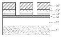
도 1a 내지 도 1e에 종래 네거티브 톤의 이중 패터닝 공정 과정을 개략적으로 도시하였다.1A to 1E schematically illustrate the process of a double patterning process of a conventional negative tone.
도 1a 및 도 1b를 참조하면, 반도체 기판(11) 상부에 비정질 탄소층(12), SiON층(13), 폴리하드마스크층(14), 제1 반사방지막(15) 및 제1 감광막(16)을 순차적으로 형성한 후, 제1 노광마스크(미도시)를 이용하여 전체 표면의 제1 영역을 노광하고, 노광된 제1 감광막(16)을 현상하여 제1 감광막 패턴(16')을 형성한다. 이때, 네거티브 톤의 이중 패터닝 공정이므로 스페이스 부분이 좁은 형태로 패턴이 형성된다. 상기 제1 감광막 패턴(16')을 식각방지막으로 하부 제1 반사방지막(15) 및 폴리하드마스크층(14)을 식각하여 폴리하드마스크 패턴(14')을 형성한다.1A and 1B, an
도 1c를 참조하면, 상기 폴리하드마스크 패턴(14') 상부에 제2 반사방지막(17) 및 제2 감광막(18)을 순차적으로 형성한 후, 제2 노광마스크(미도시)를 이 용하여 상기 제1 영역과 겹치지 않도록 교번으로 전체 표면의 제2 영역을 노광하고 상기 제2 감광막(18)을 현상하여 제2 감광막 패턴(18')을 형성한다.Referring to FIG. 1C, after the second
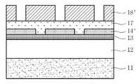
도 1d를 참조하면, 상기 제2 감광막 패턴(18')을 식각방지막으로 하부 제2 반사방지막(17) 및 폴리하드마스크층(14')을 식각하여 폴리하드마스크 패턴(14")을 형성한다.Referring to FIG. 1D, the lower second
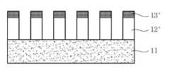
도 1e를 참조하면, 상기 폴리하드마스크 패턴(14")을 식각방지막으로 하부 SiON층(13) 및 비정질 탄소층(12)을 식각하여 원하는 미세패턴을 형성한다.Referring to FIG. 1E, the
또한, 도 2a 내지 도 2e에 종래 포지티브 톤의 이중 패터닝 공정 과정을 개략적으로 도시하였다.2a to 2e schematically illustrate a double patterning process of a conventional positive tone.
도 2a 및 도 2b를 참조하면, 반도체 기판(21) 상부에 비정질 탄소층(22), SiON층(23), 폴리하드마스크층(24), 제1 반사방지막(25) 및 제1 감광막(26)을 순차적으로 형성한 후, 제1 노광마스크(미도시)를 이용하여 전체 표면의 제1 영역을 노광하고, 노광된 제1 감광막(26)을 현상하여 제1 감광막 패턴(26')을 형성한다. 이때, 포지티브 톤의 이중 패터닝 공정이므로 라인 부분이 좁은 형태로 패턴이 형성된다. 상기 제1 감광막 패턴(26')을 식각방지막으로 하부 제1 반사방지막(25) 및 폴리하드마스크층(24)을 식각하여 폴리하드마스크 패턴(24')을 형성한다.2A and 2B, an
도 2c를 참조하면, 상기 폴리하드마스크 패턴(24') 상부에 제2 반사방지막(27) 및 제2 감광막(28)을 순차적으로 형성한 후, 제2 노광마스크(미도시)를 이용하여 상기 제1 영역과 겹치지 않도록 교번으로 전체 표면의 제2 영역을 노광하고 상기 제2 감광막(28)을 현상하여 제2 감광막 패턴(28')을 형성한다.Referring to FIG. 2C, after the second
도 2d를 참조하면, 상기 제2 감광막 패턴(28')을 식각방지막으로 하부 제2 반사방지막(27)을 식각하여 폴리하드마스크 패턴(24') 및 반사방지막 패턴(27')을 형성한다.Referring to FIG. 2D, the lower second
도 2e를 참조하면, 상기 폴리하드마스크 패턴(24') 및 반사방지막 패턴(27')을 식각방지막으로 하부 SiON층(23) 및 비정질 탄소층(22)을 식각하여 원하는 미세패턴을 형성한다.Referring to FIG. 2E, the
상기 네거티브 톤과 포지티브 톤의 이중 패터닝 공정에서, 폴리하드마스크를 하부물질의 식각방지막으로 사용하는 이중 패터닝 공정은 하부층과의 식각 선택비상 폴리하드마스크의 두께가 1,000 Å 이상 되어야 하므로, 통상의 반사방지용 조성물로는 단차가 형성된 폴리하드마스크 마루에 기판 반사율이 1.0% 이하로 코팅되는 두께로 반사방지막을 형성할 수 없어 종래에 적용되던 폴리-실리콘, 텅스텐, 질화막, 산화막 하드마스크를 배리어로 사용하는 구조 대신 상기와 같이 SiON/비정질 탄소층을 사용하는 구조를 적용할 수밖에 없다. 이는 네거티브 톤과 포지티브 톤 모두 비정질 탄소층 증착, 경사(bevel) 식각, SiON 증착, 식각 공정이 추가되어야만 하므로 공정수가 복잡해지고, 또한 화학기상증착법(chemical vapor deposition, CVD)을 이용하므로 제조 원가가 높아지는 단점이 있다. 아울러, 웨이퍼마다 두개의 마스크가 적용되기 때문에 쓰루풋(throughput) 저하는 물론, 셀 영역에서 해상도 한계에 근접한 패턴을 형성시키는 경우 디자인 룰이 감소함에 따라 공간 이미지(aerial image)가 중첩되어 원하는 해상도를 얻을 수 없게 된다. 또한, 마스크 배열시 오차로 인한 정렬불량도 큰 문제이다.In the double patterning process of the negative tone and the positive tone, the double patterning process using the polyhard mask as an etch barrier of the underlying material, the thickness of the etch selective emergency polyhard mask with the underlying layer should be more than 1,000 Å, the conventional anti-reflection As the composition, it is not possible to form an anti-reflection film with a thickness of which the substrate reflectance is coated at 1.0% or less on the poly hardmask floor having a step, and thus a structure using a poly-silicon, tungsten, nitride film, and oxide hard mask conventionally applied as a barrier Instead, there is no choice but to apply a structure using a SiON / amorphous carbon layer as described above. This is because both the negative tone and the positive tone require the addition of amorphous carbon layer deposition, bevel etching, SiON deposition, and etching processes, which increases the number of processes and increases the manufacturing cost due to the use of chemical vapor deposition (CVD). There are disadvantages. In addition, since two masks are applied to each wafer, throughput is reduced, and when a pattern near the resolution limit is formed in the cell area, the spatial image overlaps as the design rule decreases to obtain a desired resolution. It becomes impossible. In addition, misalignment due to an error in mask arrangement is also a big problem.
본 발명은 상기와 같은 종래 반도체 소자의 패턴 형성 방법 상의 문제점을 해결하기 위하여 안출된 것으로서, 실리콘을 포함하는 반사방지막 및 C-리치 폴리머를 이용하여 이중 패터닝 공정을 수행하는 것을 특징으로 하는 반도체 소자의 패턴 형성 방법을 제공하는 것을 목적으로 한다.The present invention has been made to solve the above problems in the conventional method of forming a pattern of a semiconductor device, the semiconductor device, characterized in that to perform a double patterning process using an anti-reflection film containing silicon and C-rich polymer It is an object to provide a pattern formation method.
본 발명의 반도체 소자의 패턴 형성 방법은, 반도체 기판 상부에 C-리치 폴리머, 실리콘을 포함하는 반사방지막 및 감광막을 순차적으로 형성한 후, 이중 패터닝 공정을 수행하는 것을 특징으로 한다. 상기 패터닝 공정은 네거티브 톤과 포지티브 톤의 이중 패터닝 공정 모두에 제한없이 적용될 수 있다.The method of forming a pattern of a semiconductor device according to the present invention is characterized in that a double patterning process is performed after sequentially forming an anti-reflection film and a photoresist including C-rich polymer and silicon on the semiconductor substrate. The patterning process can be applied without limitation to both the double patterning process of negative tone and positive tone.
본 명세서에 있어서, "실리콘을 포함하는 반사방지막"은 충분한 양의 실리콘을 포함하여 식각 선택비를 증진시키는 하드 마스크 역할과 패턴의 균일도 향상을 위해 193 nm ArF 파장에서 흡광도가 있는 물질을 함유하여 하부 반사방지막 역할을 동시에 할 수 있다. 실리콘을 포함하는 반사방지막은 CF4 류의 가스로 건식 식각되는 것은 물론이며 별도의 습식 화학물질(wet chemical)로도 제거될 수 있다. 또한, "C-리치 폴리머"는 탄소의 함량이 80wt% 이상인 물질로서, 비정질 탄소층의 대체 물질로 연구되고 있다. 상기 물질 모두 우수한 평탄화 성질을 갖고 있다. 실리콘을 포함하는 반사방지막 및 C-리치 폴리머 모두 스핀 코팅(spin coating) 공정을 적용하여 형성시키므로 제조 원가가 감소되고 TAT (turn-around time)가 빠른 장점이 있다.In the present specification, the "anti-reflective film containing silicon" includes a sufficient amount of silicon to serve as a hard mask to enhance the etch selectivity and to include a material having an absorbance at 193 nm ArF wavelength to improve pattern uniformity. Can act as an anti-reflection film at the same time. An anti-reflection film that includes silicon is not to be dry etched with a CF4 gas flow as well and can be removed to as a separate liquid chemical (wet chemical). In addition, "C-rich polymer" is a material having a carbon content of more than 80wt%, has been studied as an alternative to the amorphous carbon layer. All of these materials have excellent planarization properties. Since both the anti-reflection film and the C-rich polymer formed of silicon are formed by applying a spin coating process, manufacturing cost is reduced and turn-around time is fast.
이하, 첨부된 도면을 참고하여 본 발명을 상세히 설명한다.Hereinafter, with reference to the accompanying drawings will be described in detail the present invention.
본 발명의 반도체 소자의 패턴 형성 방법 중 네거티브 톤의 이중 패터닝 공정은The double patterning process of negative tone in the pattern formation method of the semiconductor device of the present invention
(1) 반도체 기판 상부에 피식각층, C-리치 폴리머층, 실리콘을 포함하는 제1 반사방지막 및 제1 감광막을 순차적으로 형성한 후, 상기 제1 감광막을 노광 및 현상하여 제1 감광막 패턴을 형성하는 단계;(1) sequentially forming an etched layer, a C-rich polymer layer, a first antireflection film containing silicon and a first photoresist film on the semiconductor substrate, and then exposing and developing the first photoresist film to form a first photoresist film pattern. Doing;
(2) 상기 제1 감광막 패턴을 식각 방지막으로 제1 반사방지막 및 C-리치 폴리머층을 식각하여 C-리치 폴리머층 패턴을 형성하는 단계;(2) etching the first anti-reflection film and the C-rich polymer layer using the first photoresist pattern as an etch stop layer to form a C-rich polymer layer pattern;
(3) 상기 C-리치 폴리머층 패턴 상부에 실리콘을 포함하는 제2 반사방지막 및 제2 감광막을 순차적으로 형성하고, 제1 반사방지막 패턴과 겹치지 않는 영역을 노광 후 현상하여 제2 감광막 패턴을 형성하는 단계;(3) sequentially forming a second anti-reflection film and a second photoresist film containing silicon on the C-rich polymer layer pattern, and developing a second photoresist pattern by exposing and developing a region that does not overlap the first anti-reflection film pattern. Doing;
(4) 상기 제2 감광막 패턴을 식각 방지막으로 제2 반사방지막 및 C-리치 폴리머층을 식각하여 C-리치 폴리머층 패턴을 형성하는 단계; 및(4) etching the second anti-reflection film and the C-rich polymer layer using the second photoresist pattern as an etch stop layer to form a C-rich polymer layer pattern; And
(5) 상기 C-리치 폴리머 패턴 사이에 존재하는 반사방지막 물질을 제거한 후 상기 C-리치 폴리머층 패턴을 식각방지막으로 하부 피식각층을 식각하여 피식각층 패턴을 형성하는 단계를 포함한다.(5) removing the anti-reflection film material present between the C-rich polymer patterns and then etching the lower etched layer using the C-rich polymer layer pattern as an etch stop layer to form an etched layer pattern.
도 3a 내지 도 3h에 본 발명에 따른 반도체 소자의 패턴 형성 방법 중 네거티브 톤의 이중 패터닝 공정 과정을 도시하였다.3A to 3H illustrate a double tone patterning process of negative tones in a method of forming a semiconductor device according to the present invention.
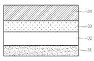
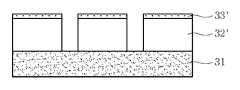
도 3a 및 도 3b를 참조하면, 실리콘 질화막 등의 하부 물질(미도시)이 형성 된 반도체 기판(31) 상부에 C-리치 폴리머층(32), 실리콘을 포함하는 제1 반사방지막(33)을 식각 선택비를 확보하기에 적당한 두께로 순차적으로 형성시킨 후 그 상부에 제1 감광막(34)을 형성한다. 이때, 상기 C-리치 폴리머층(32) 및 제1 반사방지막(33)은 바람직하게는 스핀 온(Spin on) 코팅 공정으로 형성된다. 제1 노광마스크(미도시)를 이용하여 전체 표면의 제1 영역을 노광하고, 노광된 제1 감광막(34)을 현상하여 제1 감광막 패턴(34')을 형성한다. 이때, 네거티브 톤의 이중 패터닝 공정이므로 스페이스 부분이 좁은 형태로 패턴이 형성되며, 패턴 주기의 두배의 주기를 갖도록 패턴을 형성한다.3A and 3B, a C-
도 3c를 참조하면, 상기 제1 감광막 패턴(34')을 식각방지막으로 하부 제1 반사방지막(33)을 식각하여 제1 반사방지막 패턴(33')을 형성하고, 제1 반사방지막 패턴(33')을 식각방지막으로 하부 C-리치 폴리머층(32)을 식각하여 C-리치 폴리머층 패턴(32')을 형성한다. 이때, 제1 반사방지막(33) 식각시에는 CF4, O2 가스를 단독으로 사용하거나 또는 이들을 조합하여 사용하는 것이 바람직하며, C-리치 폴리머층(32) 식각시에는 O2, N2, H2 가스를 단독으로 사용하거나 또는 이들을 조합하여 사용하는 것이 바람직하다. C-리치 폴리머층의 식각이 완료되었을 때 C-리치 폴리머층 패턴(32') 위에는 제1 반사방지막 패턴(33')이 약간 남아 있을 수도 있다.Referring to FIG. 3C, the lower
도 3d 및 도 3e를 참조하면, 별도의 습식 화학물질을 사용하여 제1 반사방지막 패턴(33') 만을 선택적으로 제거하거나 또는 이를 제거하지 않은 후, 상기 C-리 치 폴리머층 패턴(32') 상부에 식각 선택비를 확보하기에 적당한 두께로 실리콘을 포함하는 제2 반사방지막(35) 및 제2 감광막(36)을 순차적으로 형성한 후, 제2 노광마스크(미도시)를 이용하여 상기 제1 영역과 겹치지 않도록 교번으로 전체 표면의 제2 영역을 노광하고 상기 제2 감광막(36)을 현상하여 제2 감광막 패턴(36')을 형성한다.Referring to FIGS. 3D and 3E, the C-rich
도 3f 및 도 3g를 참조하면, 상기 제2 감광막 패턴(36')을 식각방지막으로 하부 제2 반사방지막(35)을 식각하여 제2 반사방지막 패턴(35')을 형성하고, 제2 반사방지막 패턴(35')을 식각방지막으로 하부 C-리치 폴리머층(32')을 식각하여 C-리치 폴리머층 패턴(32")을 형성한다. 이때, 제2 반사방지막(35) 식각시에는 CF4, O2 가스를 단독으로 사용하거나 또는 이들을 조합하여 사용하는 것이 바람직하며, C-리치 폴리머층(32') 식각시에는 O2, N2, H2 가스를 단독으로 사용하거나 또는 이들을 조합하여 사용하는 것이 바람직하다.3F and 3G, the
도 3h를 참조하면, 제1 영역의 노광 및 식각 공정시 형성된 패턴에 채워져 있는 반사방지막을 상기 반사방지막 만을 선택적으로 제거할 수 있는 화합물을 이용하여 제거한다. 이때, 상기 화합물로는 불소, 알칼리계 화합물, 또는 이들의 조합 중에서 임의로 선택될 수 있다. 이후, 상기 C-리치 폴리머층 패턴(32")을 식각 방지막으로 실리콘 질화막 등의 하부 물질(미도시)을 식각한다.Referring to FIG. 3H, the anti-reflection film filled in the pattern formed during the exposure and etching process of the first region is removed using a compound capable of selectively removing the anti-reflection film. In this case, the compound may be optionally selected from fluorine, an alkali compound, or a combination thereof. Subsequently, a lower material (not shown) such as a silicon nitride layer is etched using the C-rich
또한, 본 발명의 반도체 소자의 패턴 형성 방법 중 포지티브 톤의 이중 패터닝 공정은In addition, the double patterning process of the positive tone in the pattern formation method of the semiconductor device of the present invention
(1) 반도체 기판 상부에 피식각층, C-리치 폴리머층, 실리콘을 포함하는 제1 반사방지막 및 제1 감광막을 순차적으로 형성한 후, 상기 제1 감광막을 노광 및 현상하여 제1 감광막 패턴을 형성하는 단계;(1) sequentially forming an etched layer, a C-rich polymer layer, a first antireflection film containing silicon and a first photoresist film on the semiconductor substrate, and then exposing and developing the first photoresist film to form a first photoresist film pattern. Doing;
(2) 상기 제1 감광막 패턴을 식각 방지막으로 제1 반사방지막을 식각하여 제1 반사방지막 패턴을 형성하고, 상기 제1 반사방지막 패턴 상부에 제2 C-리치 폴리머층, 실리콘을 포함하는 제2 반사방지막 및 제2 감광막을 순차적으로 형성하는 단계;(2) forming a first anti-reflection film pattern by etching the first anti-reflection film using the first photoresist pattern as an etch stop layer, and including a second C-rich polymer layer and silicon on the first anti-reflection film pattern Sequentially forming an anti-reflection film and a second photosensitive film;
(3) 제1 반사방지막 패턴과 겹치지 않는 영역을 노광 후 현상하여 제2 감광막 패턴을 형성하고, 제2 감광막 패턴을 식각 방지막으로 제2 반사방지막 및 C-리치 폴리머층을 식각하여 C-리치 폴리머층 패턴을 형성하는 단계; 및(3) The second photoresist pattern is formed by exposing and developing a region that does not overlap the first antireflection film pattern, and the second antireflection film and the C-rich polymer layer are etched using the second photoresist pattern as an etch stop layer to form a C-rich polymer. Forming a layer pattern; And
(4) 상기 C-리치 폴리머층 패턴을 식각방지막으로 하부 피식각층을 식각하여 피식각층 패턴을 형성하는 단계를 포함한다.(4) forming the etched layer pattern by etching the lower etched layer using the C-rich polymer layer pattern as an etch stop layer.
도 4a 내지 도 4g에 본 발명에 따른 반도체 소자의 패턴 형성 방법 중 포지티브 톤의 이중 패터닝 공정 과정을 도시하였다.4A to 4G illustrate a double tone patterning process of positive tones in a method of forming a semiconductor device according to the present invention.
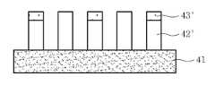
도 4a 및 도 4b를 참조하면, 실리콘 질화막 등의 하부 물질(미도시)이 형성된 반도체 기판(41) 상부에 제1 C-리치 폴리머층(42), 실리콘을 포함하는 제1 반사방지막(43)을 식각 선택비를 확보하기에 적당한 두께로 순차적으로 형성시킨 후 그 상부에 제1 감광막(44)을 형성한다. 이때, 상기 제1 C-리치 폴리머층(42) 및 제1 반사방지막(43)은 바람직하게는 스핀 온 코팅 공정으로 형성된다. 제1 노광마스크(미도시)를 이용하여 전체 표면의 제1 영역을 노광하고, 노광된 제1 감광막(44) 을 현상하여 제1 감광막 패턴(44')을 형성한다. 이때, 포지티브 톤의 이중 패터닝 공정이므로 라인 부분이 좁은 형태로 패턴이 형성되며, 패턴 주기의 두배의 주기를 갖도록 패턴을 형성한다.4A and 4B, a first C-
도 4c를 참조하면, 상기 제1 감광막 패턴(44')을 식각방지막으로 하부 제1 반사방지막(43)을 식각하여 제1 반사방지막 패턴(43')을 형성하고, 이후 남아 있는 감광막은 시너(thinner)로 제거한다. 실리콘을 포함하는 반사방지막(43)과 C-리치 폴리머층(42)은 일반적으로 감광제의 베이크(bake) 온도보다 고온인 200℃ 이상에서 베이크하여 가교결합 되므로 시너의 처리에 의해서는 제거되지 않는다. 이때, 제1 반사방지막(43) 식각시에는 CF4, O2 가스를 단독으로 사용하거나 또는 이들을 조합하여 사용하는 것이 바람직하다.Referring to FIG. 4C, the first
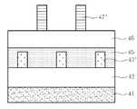
도 4d 및 도 4e를 참조하면, 상기 제1 반사방지막 패턴(43') 상부에 제2 C-리치 폴리머층(45), 실리콘을 포함하는 제2 반사방지막(46) 및 제2 감광막(47)을 순차적으로 형성한 후, 제2 노광마스크(미도시)를 이용하여 상기 제1 영역과 겹치지 않도록 교번으로 전체 표면의 제2 영역을 노광하고 상기 제2 감광막(47)을 현상하여 제2 감광막 패턴(47')을 형성한다. 상기 C-리치 폴리머는 우수한 평탄화 성질을 갖고 있기 때문에 제1 반사방지막 패턴(43') 위로 평탄하게 코팅된다.4D and 4E, the second C-
도 4f를 참조하면, 상기 제2 감광막 패턴(47')을 식각방지막으로 하부 제2 반사방지막(46)을 식각하여 제2 반사방지막 패턴(46')을 형성한다. 이때, 제2 반사방지막(46) 식각시에는 CF4, O2 가스를 단독으로 사용하거나 또는 이들을 조합하 여 사용하는 것이 바람직하다.Referring to FIG. 4F, the
도 4g를 참조하면, 제2 반사방지막 패턴(46')을 식각방지막으로 하부 C-리치 폴리머층(42,45)을 식각하여 C-리치 폴리머층 패턴(42')을 형성한다. 이때, C-리치 폴리머층(42,45) 식각시에는 O2, N2, H2 가스를 단독으로 사용하거나 또는 이들을 조합하여 사용하는 것이 바람직하다. 이 때, 식각할 C-리치 폴리머층(42,45)의 두께가 높아 식각 선택비상 제2 반사방지막 패턴(46')이 완전히 제거되고 C-리치 폴리머층(42,45)이 드러나 식각될 가능성도 있으나, 상기 도 4f에 도시된 공정에서 CD (Critical Dimension)가 결정되기 때문에 C-리치 폴리머층(42,45)이 식각되더라도 CD의 변화는 없게 된다. 이후, 상기 C-리치 폴리머층 패턴(42')을 식각 방지막으로 실리콘 질화막 등의 하부 물질(미도시)을 식각한다.Referring to FIG. 4G, the lower C-rich polymer layers 42 and 45 are etched using the second
상기에서 살펴본 바와 같이, 본 발명의 패턴 형성 방법은 이중 패터닝 공정을 이용함으로써 노광 장비의 해상한계 이하의 패턴을 용이하게 형성할 수 있으며, 또한 우수한 평탄화 성질을 갖고 있는 C-리치 폴리머와 식각 선택비를 증진시키는 하드 마스크 역할과 패턴의 균일도 향상을 동시에 충족시킬 수 있는 실리콘을 포함하는 반사방지막을 사용함으로써 제조 원가를 감소시키고 TAT가 빠른 장점이 있다.As described above, the pattern forming method of the present invention can easily form a pattern below the resolution limit of the exposure equipment by using the double patterning process, and also has a C-rich polymer having an excellent planarization property and an etching selectivity. By using an anti-reflection film containing silicon that can simultaneously satisfy the role of the hard mask and improve the uniformity of the pattern, the manufacturing cost is reduced and the TAT is fast.
Claims (7)
Translated fromKoreanPriority Applications (2)
| Application Number | Priority Date | Filing Date | Title |
|---|---|---|---|
| KR1020060064400AKR100876808B1 (en) | 2006-07-10 | 2006-07-10 | Pattern formation method of semiconductor device |
| US11/739,651US20080009138A1 (en) | 2006-07-10 | 2007-04-24 | Method for forming pattern of a semiconductor device |
Applications Claiming Priority (1)
| Application Number | Priority Date | Filing Date | Title |
|---|---|---|---|
| KR1020060064400AKR100876808B1 (en) | 2006-07-10 | 2006-07-10 | Pattern formation method of semiconductor device |
Publications (2)
| Publication Number | Publication Date |
|---|---|
| KR20080005716Atrue KR20080005716A (en) | 2008-01-15 |
| KR100876808B1 KR100876808B1 (en) | 2009-01-07 |
Family
ID=38919587
Family Applications (1)
| Application Number | Title | Priority Date | Filing Date |
|---|---|---|---|
| KR1020060064400AExpired - Fee RelatedKR100876808B1 (en) | 2006-07-10 | 2006-07-10 | Pattern formation method of semiconductor device |
Country Status (2)
| Country | Link |
|---|---|
| US (1) | US20080009138A1 (en) |
| KR (1) | KR100876808B1 (en) |
Cited By (4)
| Publication number | Priority date | Publication date | Assignee | Title |
|---|---|---|---|---|
| KR100979245B1 (en)* | 2008-11-06 | 2010-08-31 | 주식회사 하이닉스반도체 | Method of manufacturing semiconductor device |
| KR101064525B1 (en)* | 2008-04-25 | 2011-09-14 | 도쿄엘렉트론가부시키가이샤 | An etching mask formation method, an etching method, and the manufacturing method of the semiconductor device containing this etching method |
| KR101120184B1 (en)* | 2010-05-07 | 2012-02-27 | 주식회사 하이닉스반도체 | Method for forming the pattern of semiconductor device |
| US8173357B2 (en) | 2008-04-25 | 2012-05-08 | Tokyo Electron Limited | Method of forming etching mask, etching method using the etching mask, and method of fabricating semiconductor device including the etching method |
Families Citing this family (18)
| Publication number | Priority date | Publication date | Assignee | Title |
|---|---|---|---|---|
| US20080286698A1 (en)* | 2007-05-18 | 2008-11-20 | Haoren Zhuang | Semiconductor device manufacturing methods |
| KR100919564B1 (en)* | 2007-06-29 | 2009-10-01 | 주식회사 하이닉스반도체 | Method for Forming Fine Pattern of Semiconductor Device |
| NL1035771A1 (en)* | 2007-08-20 | 2009-02-23 | Asml Netherlands Bv | Lithographic Method and Method for Testing a Lithographic Apparatus. |
| KR101269054B1 (en)* | 2007-09-28 | 2013-05-29 | 삼성전자주식회사 | Method of forming fine patterns of semiconductor device |
| US8293460B2 (en)* | 2008-06-16 | 2012-10-23 | Applied Materials, Inc. | Double exposure patterning with carbonaceous hardmask |
| US20100055624A1 (en)* | 2008-08-26 | 2010-03-04 | Tokyo Electron Limited | Method of patterning a substrate using dual tone development |
| US8257911B2 (en)* | 2008-08-26 | 2012-09-04 | Tokyo Electron Limited | Method of process optimization for dual tone development |
| US9626511B2 (en)* | 2008-08-26 | 2017-04-18 | Symantec Corporation | Agentless enforcement of application management through virtualized block I/O redirection |
| US8129080B2 (en)* | 2008-09-19 | 2012-03-06 | Tokyo Electron Limited | Variable resist protecting groups |
| US8197996B2 (en)* | 2008-09-19 | 2012-06-12 | Tokyo Electron Limited | Dual tone development processes |
| JP2010199519A (en)* | 2009-02-27 | 2010-09-09 | Elpida Memory Inc | Pattern forming method |
| US8568964B2 (en)* | 2009-04-27 | 2013-10-29 | Tokyo Electron Limited | Flood exposure process for dual tone development in lithographic applications |
| US8574810B2 (en)* | 2009-04-27 | 2013-11-05 | Tokyo Electron Limited | Dual tone development with a photo-activated acid enhancement component in lithographic applications |
| CN102455591A (en)* | 2010-10-14 | 2012-05-16 | 京东方科技集团股份有限公司 | Thin film pattern and manufacturing method of array substrate |
| US8298953B2 (en)* | 2010-12-20 | 2012-10-30 | Infineon Technologies Ag | Method for defining a separating structure within a semiconductor device |
| US8728721B2 (en) | 2011-08-08 | 2014-05-20 | Micron Technology, Inc. | Methods of processing substrates |
| US8962484B2 (en)* | 2011-12-16 | 2015-02-24 | Taiwan Semiconductor Manufacturing Company, Ltd. | Method of forming pattern for semiconductor device |
| CN116741626A (en)* | 2022-03-04 | 2023-09-12 | 长鑫存储技术有限公司 | Preparation method of semiconductor structure and semiconductor structure |
Family Cites Families (7)
| Publication number | Priority date | Publication date | Assignee | Title |
|---|---|---|---|---|
| KR100223325B1 (en)* | 1995-12-15 | 1999-10-15 | 김영환 | Method for manufacturing fine pattern of semiconductor device |
| US6605545B2 (en)* | 2001-06-01 | 2003-08-12 | United Microelectronics Corp. | Method for forming hybrid low-K film stack to avoid thermal stress effect |
| US7226853B2 (en)* | 2001-12-26 | 2007-06-05 | Applied Materials, Inc. | Method of forming a dual damascene structure utilizing a three layer hard mask structure |
| KR100506876B1 (en)* | 2002-10-25 | 2005-08-04 | 주식회사 하이닉스반도체 | Manufacturing method for semiconductor device |
| KR100584042B1 (en)* | 2003-12-30 | 2006-05-29 | 동부일렉트로닉스 주식회사 | Pattern Formation Method |
| KR20050074759A (en)* | 2004-01-14 | 2005-07-19 | 주식회사 하이닉스반도체 | Method of forming ultra fine contact hole for semiconductor device |
| KR100539257B1 (en)* | 2004-04-07 | 2005-12-27 | 삼성전자주식회사 | Semiconductor structure for forming pattern and method for forming pattern |
- 2006
- 2006-07-10KRKR1020060064400Apatent/KR100876808B1/ennot_activeExpired - Fee Related
- 2007
- 2007-04-24USUS11/739,651patent/US20080009138A1/ennot_activeAbandoned
Cited By (4)
| Publication number | Priority date | Publication date | Assignee | Title |
|---|---|---|---|---|
| KR101064525B1 (en)* | 2008-04-25 | 2011-09-14 | 도쿄엘렉트론가부시키가이샤 | An etching mask formation method, an etching method, and the manufacturing method of the semiconductor device containing this etching method |
| US8173357B2 (en) | 2008-04-25 | 2012-05-08 | Tokyo Electron Limited | Method of forming etching mask, etching method using the etching mask, and method of fabricating semiconductor device including the etching method |
| KR100979245B1 (en)* | 2008-11-06 | 2010-08-31 | 주식회사 하이닉스반도체 | Method of manufacturing semiconductor device |
| KR101120184B1 (en)* | 2010-05-07 | 2012-02-27 | 주식회사 하이닉스반도체 | Method for forming the pattern of semiconductor device |
Also Published As
| Publication number | Publication date |
|---|---|
| US20080009138A1 (en) | 2008-01-10 |
| KR100876808B1 (en) | 2009-01-07 |
Similar Documents
| Publication | Publication Date | Title |
|---|---|---|
| KR100876808B1 (en) | Pattern formation method of semiconductor device | |
| US7354847B2 (en) | Method of trimming technology | |
| US7540970B2 (en) | Methods of fabricating a semiconductor device | |
| US9373580B2 (en) | Dual hard mask lithography process | |
| TWI424469B (en) | Double patterning strategy for contact hole and trench | |
| KR101087835B1 (en) | Method of forming fine pattern of semiconductor device | |
| KR101004691B1 (en) | Method of forming fine pattern of semiconductor device | |
| JP2004153125A (en) | Method of forming processing mask and method of manufacturing semiconductor device | |
| KR20070076793A (en) | Method of forming fine pattern of semiconductor device | |
| KR20070005912A (en) | Structures including variable antireflective coatings and methods of forming the same | |
| JP2009071306A (en) | Method for forming micropattern in semiconductor device | |
| CN112017946A (en) | Forming method of semiconductor structure and transistor | |
| TW201916101A (en) | Method for forming openings in underlayer | |
| US7396751B2 (en) | Method for manufacturing semiconductor device | |
| KR100843899B1 (en) | Manufacturing method of semiconductor device | |
| US8524608B1 (en) | Method for fabricating a patterned structure of a semiconductor device | |
| CN111640657B (en) | Semiconductor device and method of forming the same | |
| CN101188188A (en) | patterning method | |
| TWI443758B (en) | Method of forming gate conductor structures | |
| CN103441067B (en) | Be applied to the double-pattern forming method of grid line end cutting | |
| KR20070113604A (en) | Method of forming fine pattern of semiconductor device | |
| TWI515768B (en) | Lithography patterning method and double patterning method | |
| US8129094B2 (en) | Method for manufacturing a semiconductor device | |
| US11309184B2 (en) | Semiconductor structure and formation method thereof | |
| TWI473205B (en) | Method for forming contact hole |
Legal Events
| Date | Code | Title | Description |
|---|---|---|---|
| PA0109 | Patent application | St.27 status event code:A-0-1-A10-A12-nap-PA0109 | |
| R17-X000 | Change to representative recorded | St.27 status event code:A-3-3-R10-R17-oth-X000 | |
| A201 | Request for examination | ||
| P11-X000 | Amendment of application requested | St.27 status event code:A-2-2-P10-P11-nap-X000 | |
| P13-X000 | Application amended | St.27 status event code:A-2-2-P10-P13-nap-X000 | |
| PA0201 | Request for examination | St.27 status event code:A-1-2-D10-D11-exm-PA0201 | |
| PG1501 | Laying open of application | St.27 status event code:A-1-1-Q10-Q12-nap-PG1501 | |
| D13-X000 | Search requested | St.27 status event code:A-1-2-D10-D13-srh-X000 | |
| D14-X000 | Search report completed | St.27 status event code:A-1-2-D10-D14-srh-X000 | |
| E902 | Notification of reason for refusal | ||
| PE0902 | Notice of grounds for rejection | St.27 status event code:A-1-2-D10-D21-exm-PE0902 | |
| P11-X000 | Amendment of application requested | St.27 status event code:A-2-2-P10-P11-nap-X000 | |
| P13-X000 | Application amended | St.27 status event code:A-2-2-P10-P13-nap-X000 | |
| E701 | Decision to grant or registration of patent right | ||
| PE0701 | Decision of registration | St.27 status event code:A-1-2-D10-D22-exm-PE0701 | |
| GRNT | Written decision to grant | ||
| PR0701 | Registration of establishment | St.27 status event code:A-2-4-F10-F11-exm-PR0701 | |
| PR1002 | Payment of registration fee | St.27 status event code:A-2-2-U10-U11-oth-PR1002 Fee payment year number:1 | |
| PG1601 | Publication of registration | St.27 status event code:A-4-4-Q10-Q13-nap-PG1601 | |
| LAPS | Lapse due to unpaid annual fee | ||
| PC1903 | Unpaid annual fee | St.27 status event code:A-4-4-U10-U13-oth-PC1903 Not in force date:20111224 Payment event data comment text:Termination Category : DEFAULT_OF_REGISTRATION_FEE | |
| PN2301 | Change of applicant | St.27 status event code:A-5-5-R10-R13-asn-PN2301 St.27 status event code:A-5-5-R10-R11-asn-PN2301 | |
| PC1903 | Unpaid annual fee | St.27 status event code:N-4-6-H10-H13-oth-PC1903 Ip right cessation event data comment text:Termination Category : DEFAULT_OF_REGISTRATION_FEE Not in force date:20111224 | |
| PN2301 | Change of applicant | St.27 status event code:A-5-5-R10-R13-asn-PN2301 St.27 status event code:A-5-5-R10-R11-asn-PN2301 | |
| PN2301 | Change of applicant | St.27 status event code:A-5-5-R10-R13-asn-PN2301 St.27 status event code:A-5-5-R10-R11-asn-PN2301 |