KR20070121403A - Electrophoretic display device and manufacturing method thereof - Google Patents
Electrophoretic display device and manufacturing method thereofDownload PDFInfo
- Publication number
- KR20070121403A KR20070121403AKR1020060056435AKR20060056435AKR20070121403AKR 20070121403 AKR20070121403 AKR 20070121403AKR 1020060056435 AKR1020060056435 AKR 1020060056435AKR 20060056435 AKR20060056435 AKR 20060056435AKR 20070121403 AKR20070121403 AKR 20070121403A
- Authority
- KR
- South Korea
- Prior art keywords
- electrophoretic
- display device
- electrophoretic particles
- color
- particles
- Prior art date
- Legal status (The legal status is an assumption and is not a legal conclusion. Google has not performed a legal analysis and makes no representation as to the accuracy of the status listed.)
- Withdrawn
Links
Images


Classifications
- G—PHYSICS
- G02—OPTICS
- G02F—OPTICAL DEVICES OR ARRANGEMENTS FOR THE CONTROL OF LIGHT BY MODIFICATION OF THE OPTICAL PROPERTIES OF THE MEDIA OF THE ELEMENTS INVOLVED THEREIN; NON-LINEAR OPTICS; FREQUENCY-CHANGING OF LIGHT; OPTICAL LOGIC ELEMENTS; OPTICAL ANALOGUE/DIGITAL CONVERTERS
- G02F1/00—Devices or arrangements for the control of the intensity, colour, phase, polarisation or direction of light arriving from an independent light source, e.g. switching, gating or modulating; Non-linear optics
- G02F1/01—Devices or arrangements for the control of the intensity, colour, phase, polarisation or direction of light arriving from an independent light source, e.g. switching, gating or modulating; Non-linear optics for the control of the intensity, phase, polarisation or colour
- G02F1/13—Devices or arrangements for the control of the intensity, colour, phase, polarisation or direction of light arriving from an independent light source, e.g. switching, gating or modulating; Non-linear optics for the control of the intensity, phase, polarisation or colour based on liquid crystals, e.g. single liquid crystal display cells
- G02F1/133—Constructional arrangements; Operation of liquid crystal cells; Circuit arrangements
- G02F1/1333—Constructional arrangements; Manufacturing methods
- G02F1/133377—Cells with plural compartments or having plurality of liquid crystal microcells partitioned by walls, e.g. one microcell per pixel
- G—PHYSICS
- G02—OPTICS
- G02F—OPTICAL DEVICES OR ARRANGEMENTS FOR THE CONTROL OF LIGHT BY MODIFICATION OF THE OPTICAL PROPERTIES OF THE MEDIA OF THE ELEMENTS INVOLVED THEREIN; NON-LINEAR OPTICS; FREQUENCY-CHANGING OF LIGHT; OPTICAL LOGIC ELEMENTS; OPTICAL ANALOGUE/DIGITAL CONVERTERS
- G02F1/00—Devices or arrangements for the control of the intensity, colour, phase, polarisation or direction of light arriving from an independent light source, e.g. switching, gating or modulating; Non-linear optics
- G02F1/01—Devices or arrangements for the control of the intensity, colour, phase, polarisation or direction of light arriving from an independent light source, e.g. switching, gating or modulating; Non-linear optics for the control of the intensity, phase, polarisation or colour
- G02F1/165—Devices or arrangements for the control of the intensity, colour, phase, polarisation or direction of light arriving from an independent light source, e.g. switching, gating or modulating; Non-linear optics for the control of the intensity, phase, polarisation or colour based on translational movement of particles in a fluid under the influence of an applied field
- G02F1/1675—Constructional details
- G02F1/1679—Gaskets; Spacers; Sealing of cells; Filling or closing of cells
- G02F1/1681—Gaskets; Spacers; Sealing of cells; Filling or closing of cells having two or more microcells partitioned by walls, e.g. of microcup type
- G—PHYSICS
- G02—OPTICS
- G02F—OPTICAL DEVICES OR ARRANGEMENTS FOR THE CONTROL OF LIGHT BY MODIFICATION OF THE OPTICAL PROPERTIES OF THE MEDIA OF THE ELEMENTS INVOLVED THEREIN; NON-LINEAR OPTICS; FREQUENCY-CHANGING OF LIGHT; OPTICAL LOGIC ELEMENTS; OPTICAL ANALOGUE/DIGITAL CONVERTERS
- G02F1/00—Devices or arrangements for the control of the intensity, colour, phase, polarisation or direction of light arriving from an independent light source, e.g. switching, gating or modulating; Non-linear optics
- G02F1/01—Devices or arrangements for the control of the intensity, colour, phase, polarisation or direction of light arriving from an independent light source, e.g. switching, gating or modulating; Non-linear optics for the control of the intensity, phase, polarisation or colour
- G02F1/165—Devices or arrangements for the control of the intensity, colour, phase, polarisation or direction of light arriving from an independent light source, e.g. switching, gating or modulating; Non-linear optics for the control of the intensity, phase, polarisation or colour based on translational movement of particles in a fluid under the influence of an applied field
- G02F1/166—Devices or arrangements for the control of the intensity, colour, phase, polarisation or direction of light arriving from an independent light source, e.g. switching, gating or modulating; Non-linear optics for the control of the intensity, phase, polarisation or colour based on translational movement of particles in a fluid under the influence of an applied field characterised by the electro-optical or magneto-optical effect
- G02F1/167—Devices or arrangements for the control of the intensity, colour, phase, polarisation or direction of light arriving from an independent light source, e.g. switching, gating or modulating; Non-linear optics for the control of the intensity, phase, polarisation or colour based on translational movement of particles in a fluid under the influence of an applied field characterised by the electro-optical or magneto-optical effect by electrophoresis
- G—PHYSICS
- G02—OPTICS
- G02F—OPTICAL DEVICES OR ARRANGEMENTS FOR THE CONTROL OF LIGHT BY MODIFICATION OF THE OPTICAL PROPERTIES OF THE MEDIA OF THE ELEMENTS INVOLVED THEREIN; NON-LINEAR OPTICS; FREQUENCY-CHANGING OF LIGHT; OPTICAL LOGIC ELEMENTS; OPTICAL ANALOGUE/DIGITAL CONVERTERS
- G02F1/00—Devices or arrangements for the control of the intensity, colour, phase, polarisation or direction of light arriving from an independent light source, e.g. switching, gating or modulating; Non-linear optics
- G02F1/01—Devices or arrangements for the control of the intensity, colour, phase, polarisation or direction of light arriving from an independent light source, e.g. switching, gating or modulating; Non-linear optics for the control of the intensity, phase, polarisation or colour
- G02F1/165—Devices or arrangements for the control of the intensity, colour, phase, polarisation or direction of light arriving from an independent light source, e.g. switching, gating or modulating; Non-linear optics for the control of the intensity, phase, polarisation or colour based on translational movement of particles in a fluid under the influence of an applied field
- G02F1/1675—Constructional details
- G02F1/16756—Insulating layers
- G—PHYSICS
- G02—OPTICS
- G02F—OPTICAL DEVICES OR ARRANGEMENTS FOR THE CONTROL OF LIGHT BY MODIFICATION OF THE OPTICAL PROPERTIES OF THE MEDIA OF THE ELEMENTS INVOLVED THEREIN; NON-LINEAR OPTICS; FREQUENCY-CHANGING OF LIGHT; OPTICAL LOGIC ELEMENTS; OPTICAL ANALOGUE/DIGITAL CONVERTERS
- G02F1/00—Devices or arrangements for the control of the intensity, colour, phase, polarisation or direction of light arriving from an independent light source, e.g. switching, gating or modulating; Non-linear optics
- G02F1/01—Devices or arrangements for the control of the intensity, colour, phase, polarisation or direction of light arriving from an independent light source, e.g. switching, gating or modulating; Non-linear optics for the control of the intensity, phase, polarisation or colour
- G02F1/165—Devices or arrangements for the control of the intensity, colour, phase, polarisation or direction of light arriving from an independent light source, e.g. switching, gating or modulating; Non-linear optics for the control of the intensity, phase, polarisation or colour based on translational movement of particles in a fluid under the influence of an applied field
- G02F1/1675—Constructional details
- G02F1/1676—Electrodes
- G02F1/16766—Electrodes for active matrices
- G—PHYSICS
- G02—OPTICS
- G02F—OPTICAL DEVICES OR ARRANGEMENTS FOR THE CONTROL OF LIGHT BY MODIFICATION OF THE OPTICAL PROPERTIES OF THE MEDIA OF THE ELEMENTS INVOLVED THEREIN; NON-LINEAR OPTICS; FREQUENCY-CHANGING OF LIGHT; OPTICAL LOGIC ELEMENTS; OPTICAL ANALOGUE/DIGITAL CONVERTERS
- G02F1/00—Devices or arrangements for the control of the intensity, colour, phase, polarisation or direction of light arriving from an independent light source, e.g. switching, gating or modulating; Non-linear optics
- G02F1/01—Devices or arrangements for the control of the intensity, colour, phase, polarisation or direction of light arriving from an independent light source, e.g. switching, gating or modulating; Non-linear optics for the control of the intensity, phase, polarisation or colour
- G02F1/165—Devices or arrangements for the control of the intensity, colour, phase, polarisation or direction of light arriving from an independent light source, e.g. switching, gating or modulating; Non-linear optics for the control of the intensity, phase, polarisation or colour based on translational movement of particles in a fluid under the influence of an applied field
- G02F1/1675—Constructional details
- G02F1/1679—Gaskets; Spacers; Sealing of cells; Filling or closing of cells
- G—PHYSICS
- G02—OPTICS
- G02F—OPTICAL DEVICES OR ARRANGEMENTS FOR THE CONTROL OF LIGHT BY MODIFICATION OF THE OPTICAL PROPERTIES OF THE MEDIA OF THE ELEMENTS INVOLVED THEREIN; NON-LINEAR OPTICS; FREQUENCY-CHANGING OF LIGHT; OPTICAL LOGIC ELEMENTS; OPTICAL ANALOGUE/DIGITAL CONVERTERS
- G02F1/00—Devices or arrangements for the control of the intensity, colour, phase, polarisation or direction of light arriving from an independent light source, e.g. switching, gating or modulating; Non-linear optics
- G02F1/01—Devices or arrangements for the control of the intensity, colour, phase, polarisation or direction of light arriving from an independent light source, e.g. switching, gating or modulating; Non-linear optics for the control of the intensity, phase, polarisation or colour
- G02F1/13—Devices or arrangements for the control of the intensity, colour, phase, polarisation or direction of light arriving from an independent light source, e.g. switching, gating or modulating; Non-linear optics for the control of the intensity, phase, polarisation or colour based on liquid crystals, e.g. single liquid crystal display cells
- G02F1/133—Constructional arrangements; Operation of liquid crystal cells; Circuit arrangements
- G02F1/1333—Constructional arrangements; Manufacturing methods
- G02F1/1341—Filling or closing of cells
- G—PHYSICS
- G02—OPTICS
- G02F—OPTICAL DEVICES OR ARRANGEMENTS FOR THE CONTROL OF LIGHT BY MODIFICATION OF THE OPTICAL PROPERTIES OF THE MEDIA OF THE ELEMENTS INVOLVED THEREIN; NON-LINEAR OPTICS; FREQUENCY-CHANGING OF LIGHT; OPTICAL LOGIC ELEMENTS; OPTICAL ANALOGUE/DIGITAL CONVERTERS
- G02F1/00—Devices or arrangements for the control of the intensity, colour, phase, polarisation or direction of light arriving from an independent light source, e.g. switching, gating or modulating; Non-linear optics
- G02F1/01—Devices or arrangements for the control of the intensity, colour, phase, polarisation or direction of light arriving from an independent light source, e.g. switching, gating or modulating; Non-linear optics for the control of the intensity, phase, polarisation or colour
- G02F1/165—Devices or arrangements for the control of the intensity, colour, phase, polarisation or direction of light arriving from an independent light source, e.g. switching, gating or modulating; Non-linear optics for the control of the intensity, phase, polarisation or colour based on translational movement of particles in a fluid under the influence of an applied field
- G02F1/1675—Constructional details
- G02F2001/1678—Constructional details characterised by the composition or particle type
- G—PHYSICS
- G02—OPTICS
- G02F—OPTICAL DEVICES OR ARRANGEMENTS FOR THE CONTROL OF LIGHT BY MODIFICATION OF THE OPTICAL PROPERTIES OF THE MEDIA OF THE ELEMENTS INVOLVED THEREIN; NON-LINEAR OPTICS; FREQUENCY-CHANGING OF LIGHT; OPTICAL LOGIC ELEMENTS; OPTICAL ANALOGUE/DIGITAL CONVERTERS
- G02F2201/00—Constructional arrangements not provided for in groups G02F1/00 - G02F7/00
- G02F2201/12—Constructional arrangements not provided for in groups G02F1/00 - G02F7/00 electrode
- G02F2201/121—Constructional arrangements not provided for in groups G02F1/00 - G02F7/00 electrode common or background
Landscapes
- Physics & Mathematics (AREA)
- Nonlinear Science (AREA)
- Optics & Photonics (AREA)
- General Physics & Mathematics (AREA)
- Chemical & Material Sciences (AREA)
- Chemical Kinetics & Catalysis (AREA)
- Electrochemistry (AREA)
- Molecular Biology (AREA)
- Life Sciences & Earth Sciences (AREA)
- Health & Medical Sciences (AREA)
- Mathematical Physics (AREA)
- Crystallography & Structural Chemistry (AREA)
- Electrochromic Elements, Electrophoresis, Or Variable Reflection Or Absorption Elements (AREA)
Abstract
Translated fromKoreanDescription
Translated fromKorean도1은 본 발명의 한 실시예에 따른 전기 영동 표시 장치의 구조를 도시한 배치도이고, 1 is a layout view illustrating a structure of an electrophoretic display device according to an exemplary embodiment of the present invention.
도2는 도1의 전기 영동 표시 소자를 II-II' 선에 따라 자른 단면도이고,FIG. 2 is a cross-sectional view of the electrophoretic display device of FIG. 1 taken along line II-II ',
도3a 내지 도3g는 본 발명의 한 실시예에 따른 전기 영동 표시 장치의 제조 방법을 순차적으로 도시한 단면도이고,3A to 3G are cross-sectional views sequentially illustrating a method of manufacturing an electrophoretic display device according to an exemplary embodiment of the present invention.
도4는 본 발명의 다른 실시예에 따른 전기 영동 표시 장치의 단면도이고,4 is a cross-sectional view of an electrophoretic display device according to another exemplary embodiment of the present invention.
도5는 본 발명의 다른 실시예에 따른 전기 영동 표시 장치의 단면도이고,5 is a cross-sectional view of an electrophoretic display device according to another exemplary embodiment of the present invention.
도6은 본 발명의 다른 실시예에 따른 전기 영동 표시 장치의 단면도, 및6 is a cross-sectional view of an electrophoretic display device according to another exemplary embodiment of the present invention; and
도7은 본 발명의 다른 실시예에 따른 전기 영동 표시 장치의 단면도이다.7 is a cross-sectional view of an electrophoretic display device according to another exemplary embodiment of the present invention.
<도면의 주요 부분에 대한 부호의 설명><Explanation of symbols for the main parts of the drawings>
1, 2, 3, 4, 5: 전기 영동 표시 장치1, 2, 3, 4, 5: electrophoresis display
100, 101, 102, 103: 박막트랜지스터 표시판100, 101, 102, 103: thin film transistor display panel
110: 절연기판 121: 게이트선110: insulation substrate 121: gate line
124: 게이트 전극 129: 게이트선의 끝부분124: gate electrode 129: end of gate line
140: 게이트 절연막 151: 선형 반도체층140: gate insulating film 151: linear semiconductor layer
161: 선형 저항성 접촉 부재 171: 데이터선161: linear ohmic contact 171: data line
173: 소스 전극 175: 드레인 전극173: source electrode 175: drain electrode
179: 데이터선의 끝부분 180: 보호막179: end of the data line 180: protective film
181, 182, 185: 접촉구 190: 화소 전극181, 182, and 185: contact hole 190: pixel electrode
191: 격벽 200: 공통 전극 표시판191: barrier 200: common electrode display panel
210: 절연 기판 220: 공통 전극210: insulating substrate 220: common electrode
230: 유기막 300: 잉크230: organic film 300: ink
310, 311, 312, 313: 전기 영동 부재310, 311, 312, 313: electrophoretic member
314, 315: 전기 영동 입자 317, 318: 분산매314, 315:
319: 캡슐319: capsule
본 발명은 전기 영동 표시 장치 및 그 제조 방법에 관한 것이다.The present invention relates to an electrophoretic display device and a manufacturing method thereof.
최근 기존의 브라운관을 대체하여 액정표시장치, 유기 전계 발광 장치(OLED) 및 전기 영동 표시 장치(ELECTROPORETIC DISPLAY) 등의 평판(flat panel)형 표시 장치가 많이 사용되고 있다.Recently, flat panel displays such as liquid crystal displays, organic light emitting diodes (OLEDs), and electrophoretic displays (ELECTROPORETIC DISPLAYs) have been used in place of existing CRTs.
이 중 전기 영동 표시 장치는 화소 전극 및 공통 전극에 인가된 전압에 따라 양 또는 음의 전하를 띠며 소정의 색상을 갖는 전기 영동 입자가 회전하거나, 화소 전극 또는 공통 전극 가까이로 이동하는 방식으로 원하는 색상을 표현한다.Among these, the electrophoretic display device has a desired color in such a manner that electrophoretic particles having a predetermined color rotate or move near the pixel electrode or the common electrode, having a positive or negative charge depending on the voltage applied to the pixel electrode and the common electrode. Express
이러한 전기 영동 표시 장치의 제조는 전기 영동 입자 및 전기 영동 입자가 분산된 분산매를 가두고 있는 마이크로 캡슐(microcapsule)을 제조한 후 이 마이크로 캡슐을 박막트랜지스터 표시판의 화소 전극 상에 배치시키는 공정을 통해 이루어진다.The electrophoretic display device is manufactured by manufacturing a microcapsule containing electrophoretic particles and a dispersion medium in which the electrophoretic particles are dispersed, and then placing the microcapsule on the pixel electrode of the thin film transistor array panel. .
그러나 전기 영동 표시 장치의 제조에 있어서 전기 영동 입자 및 전기 영동 입자가 분산된 분산매를 갖는 마이크로 캡슐을 제조하기가 용이하지 않아 제조 효율이 떨어지는 문제점이 있다. 또한 마이크로 캡슐을 제조하였더라도 박막트랜지스터 표시판의 화소 전극 상에 정확하게 배치하는 것이 용이하지 않아 표시 성능이 저하되는 문제점이 있다.However, in manufacturing an electrophoretic display device, it is not easy to manufacture a microcapsule having electrophoretic particles and a dispersion medium in which the electrophoretic particles are dispersed. In addition, even if the microcapsule is manufactured, it is not easy to accurately arrange the pixel electrode of the thin film transistor array panel, thereby degrading display performance.
따라서, 본 발명이 이루고자 하는 기술적 과제는 이러한 문제점을 해결하여 제조 효율과 표시 성능이 우수한 전기 영동 표시 장치 및 그 제조 방법을 제공하는데 있다.Accordingly, an aspect of the present invention is to solve the above problems and to provide an electrophoretic display device having excellent manufacturing efficiency and display performance and a method of manufacturing the same.
본 발명에 따른 전기 영동 표시 장치는 절연 기판 위에 형성되어 있는 박막트랜지스터, 상기 박막트랜지스터와 전기적으로 연결되어 있는 화소 전극, 상기 화소 전극 간을 구분하는 격벽, 상기 격벽 사이에 노출된 상기 화소 전극 위에 형성되어 있으며 전기 영동 부재가 분산되어 있는 잉크, 그리고 상기 잉크 및 상기 격벽 위에 형성되어 있으며 공통 전극을 갖는 공통 전극 표시판을 포함한다.An electrophoretic display device according to an exemplary embodiment of the present invention includes a thin film transistor formed on an insulating substrate, a pixel electrode electrically connected to the thin film transistor, a partition wall separating the pixel electrodes, and a pixel electrode exposed between the partition walls. And an ink in which the electrophoretic member is dispersed, and a common electrode display panel formed on the ink and the partition wall and having a common electrode.
상기 잉크 및 상기 공통 전극 사이에 형성되어 있는 유기막을 더 포함할 수 있다.The method may further include an organic layer formed between the ink and the common electrode.
상기 격벽은 유기 절연 물질 및 무기 절연 물질 중 적어도 어느 하나를 포함하여 이루어질 수 있다.The partition wall may include at least one of an organic insulating material and an inorganic insulating material.
상기 격벽은 격자 모양으로 형성될 수 있다.The partition wall may be formed in a lattice shape.
전기 영동 부재를 포함하는 상기 잉크는 젯팅(jetting) 부재에 의한 드로핑(dropping)에 의해 형성될 수 있다.The ink including the electrophoretic member may be formed by dropping by a jetting member.
상기 전기 영동 부재는 전기 영동 입자를 포함할 수 있다.The electrophoretic member may include electrophoretic particles.
상기 전기 영동 입자는, 청색, 녹색 및 적색 중 어느 하나의 색을 갖는 제1 전기 영동 입자, 그리고 검은색을 갖는 제2 전기 영동 입자를 포함할 수 있다.The electrophoretic particles may include first electrophoretic particles having any one of blue, green, and red colors, and second electrophoretic particles having black color.
상기 전기 영동 입자는, 옐로(yellow), 마젠타(magenta), 시안(cyan) 중 어느 하나의 색을 갖는 제3 전기 영동입자, 그리고 검은색을 갖는 제4 전기 영동 입자를 포함할 수 있다.The electrophoretic particles may include third electrophoretic particles having any one of yellow, magenta, and cyan, and fourth electrophoretic particles having black color.
상기 전기 영동 입자는 청색, 녹색 및 적색 중 어느 하나의 색을 가지며, 상기 잉크는 검은색을 가질 수 있다.The electrophoretic particles may have any one of blue, green, and red colors, and the ink may have black color.
상기 전기 영동 입자는 옐로(yellow), 마젠타(magenta), 시안(cyan) 중 어느 하나의 색을 가지며, 상기 잉크는 검은색을 가질 수 있다.The electrophoretic particles may have any one color of yellow, magenta, and cyan, and the ink may have black color.
상기 전기 영동 부재는, 상기 전기 영동 입자가 분산되어 있는 분산매, 그리고 상기 전기 영동 입자 및 상기 분산매를 가두고 있는 캡슐을 더 포함할 수 있다.The electrophoretic member may further include a dispersion medium in which the electrophoretic particles are dispersed, and a capsule containing the electrophoretic particles and the dispersion medium.
상기 전기 영동 입자는, 청색, 녹색 및 적색 중 어느 하나의 색을 갖는 제1 전기 영동 입자, 그리고 검은색을 갖는 제2 전기 영동 입자를 포함할 수 있다.The electrophoretic particles may include first electrophoretic particles having any one of blue, green, and red colors, and second electrophoretic particles having black color.
상기 전기 영동 입자는, 옐로(yellow), 마젠타(magenta), 시안(cyan) 중 어느 하나의 색을 갖는 제3 전기 영동입자, 그리고 검은색을 갖는 제4 전기 영동 입자를 포함할 수 있다.The electrophoretic particles may include third electrophoretic particles having any one of yellow, magenta, and cyan, and fourth electrophoretic particles having black color.
상기 전기 영동 입자는 청색, 녹색 및 적색 중 어느 하나의 색을 가지며, 상기 분산매는 검은색을 가질 수 있다.The electrophoretic particles may have any one of blue, green, and red colors, and the dispersion medium may have black color.
상기 전기 영동 입자는 옐로(yellow), 마젠타(magenta), 시안(cyan) 중 어 느 하나의 색을 가지며, 상기 분산매는 검은색을 가질 수 있다.The electrophoretic particles may have any one color of yellow, magenta, and cyan, and the dispersion medium may have a black color.
또한, 본 발명에 따른 전기 영동 표시 장치의 제조 방법은 절연 기판 위에 박막트랜지스터 및 상기 박막트랜지스터와 전기적으로 연결되는 화소 전극을 형성하는 단계, 상기 화소 전극 간을 구분하는 격벽을 형성하는 단계, 상기 격벽 사이에 노출된 상기 화소 전극 위에 전기 영동 부재가 분산되어 있는 잉크를 드로핑하는 단계, 절연기판 상에 공통 전극을 형성하여 공통 전극 표시판을 마련하는 단계, 그리고 드로핑된 상기 잉크 및 상기 격벽 위에 상기 공통 전극 표시판을 밀착하는 단계를 포함한다.In addition, the method of manufacturing an electrophoretic display device according to the present invention comprises the steps of forming a thin film transistor and a pixel electrode electrically connected to the thin film transistor on an insulating substrate, forming a partition wall separating the pixel electrodes, the partition wall Dropping an ink having an electrophoretic member dispersed thereon on the pixel electrode exposed in between, forming a common electrode on an insulating substrate to provide a common electrode display panel, and on the dropped ink and the partition wall And contacting the common electrode display panel.
상기 공통 전극 표시판을 마련하는 단계는 상기 공통 전극 위에 유기막을 형성하는 단계를 더 포함할 수 있다.The preparing of the common electrode display panel may further include forming an organic layer on the common electrode.
상기 격벽을 형성하는 단계에서, 상기 격벽은 유기 절연 물질 및 무기 절연 물질 중 적어도 어느 하나를 포함하여 형성할 수 있다.In the forming of the partition wall, the partition wall may include at least one of an organic insulating material and an inorganic insulating material.
상기 격벽을 형성하는 단계에서, 상기 격벽은 격자 모양으로 형성할 수 있다.In the forming of the partition wall, the partition wall may be formed in a grid shape.
상기 잉크를 드로핑하는 단계는, 젯팅(jetting) 부재를 이용하여 수행할 수 있다.Dropping the ink may be performed by using a jetting member.
상기 전기 영동 부재는 전기 영동 입자를 포함할 수 있다.The electrophoretic member may include electrophoretic particles.
상기 전기 영동 입자는, 청색, 녹색 및 적색 중 어느 하나의 색을 갖는 제1 전기 영동 입자, 그리고 검은색을 갖는 제2 전기 영동 입자를 포함할 수 있다.The electrophoretic particles may include first electrophoretic particles having any one of blue, green, and red colors, and second electrophoretic particles having black color.
상기 전기 영동 입자는, 옐로(yellow), 마젠타(magenta), 시안(cyan) 중 어느 하나의 색을 갖는 제3 전기 영동입자, 그리고 검은색을 갖는 제4 전기 영동 입자를 포함할 수 있다.The electrophoretic particles may include third electrophoretic particles having any one of yellow, magenta, and cyan, and fourth electrophoretic particles having black color.
상기 전기 영동 입자는 청색, 녹색 및 적색 중 어느 하나의 색을 가지며, 상기 잉크는 검은색을 가질 수 있다.The electrophoretic particles may have any one of blue, green, and red colors, and the ink may have black color.
상기 전기 영동 입자는 옐로(yellow), 마젠타(magenta), 시안(cyan) 중 어느 하나의 색을 가지며, 상기 잉크는 검은색을 가질 수 있다.The electrophoretic particles may have any one color of yellow, magenta, and cyan, and the ink may have black color.
상기 전기 영동 부재는, 상기 전기 영동 입자가 분산되어 있는 분산매, 그리고상기 전기 영동 입자 및 상기 분산매를 가두고 있는 캡슐을 더 포함할 수 있다.The electrophoretic member may further include a dispersion medium in which the electrophoretic particles are dispersed, and a capsule containing the electrophoretic particles and the dispersion medium.
상기 전기 영동 입자는, 청색, 녹색 및 적색 중 어느 하나의 색을 갖는 제1 전기 영동 입자, 그리고 검은색을 갖는 제2 전기 영동 입자를 포함할 수 있다.The electrophoretic particles may include first electrophoretic particles having any one of blue, green, and red colors, and second electrophoretic particles having black color.
상기 전기 영동 입자는, 옐로(yellow), 마젠타(magenta), 시안(cyan) 중 어느 하나의 색을 갖는 제3 전기 영동입자, 그리고 검은색을 갖는 제4 전기 영동 입자를 포함할 수 있다.The electrophoretic particles may include third electrophoretic particles having any one of yellow, magenta, and cyan, and fourth electrophoretic particles having black color.
상기 전기 영동 입자는 청색, 녹색 및 적색 중 어느 하나의 색을 가지며, 상 기 분산매는 검은색을 가질 수 있다.The electrophoretic particles may have any one color of blue, green, and red, and the dispersion medium may have black color.
상기 전기 영동 입자는 옐로(yellow), 마젠타(magenta), 시안(cyan) 중 어 느 하나의 색을 가지며, 상기 분산매는 검은색을 가질 수 있다.The electrophoretic particles may have any one color of yellow, magenta, and cyan, and the dispersion medium may have a black color.
이하에서는 첨부한 도면을 참고로 하여 본 발명의 실시예에 대하여 본 발명이 속하는 기술 분야에서 통상의 지식을 가진 자가 용이하게 실시할 수 있도록 상세히 설명한다. 그러나 본 발명은 여러 가지 상이한 형태로 구현될 수 있으며 여기에서 설명하는 실시예에 한정되지 않는다.DETAILED DESCRIPTION Hereinafter, exemplary embodiments of the present invention will be described in detail with reference to the accompanying drawings so that those skilled in the art may easily implement the present invention. As those skilled in the art would realize, the described embodiments may be modified in various different ways, all without departing from the spirit or scope of the present invention.
도면에서 여러 층 및 영역을 명확하게 표현하기 위하여 두께를 확대하여 나타내었다. 명세서 전체를 통하여 유사한 부분에 대해서는 동일한 도면 부호를 붙였다. 층, 막, 영역, 판 등의 부분이 다른 부분 “위에” 있다고 할 때, 이는 다른 부분 “바로 위에” 있는 경우뿐 아니라 그 중간에 또 다른 부분이 있는 경우도 포함한다. 반대로 어떤 부분이 다른 부분 “바로 위에” 있다고 할 때에는 중간에 다른 부분이 없는 것을 뜻한다.In the drawings, the thickness of layers, films, panels, regions, etc., are exaggerated for clarity. Like parts are designated by like reference numerals throughout the specification. When a part of a layer, film, area, plate, etc. is said to be "on" another part, this includes not only the other part "directly" but also another part in the middle. On the contrary, when a part is “just above” another part, there is no other part in the middle.
그러면 첨부한 도면을 참고로 하여 본 발명의 여러 실시예에 따른 전기 영동 표시 장치 및 그 제조 방법에 대하여 설명한다.Next, an electrophoretic display device and a manufacturing method thereof according to various embodiments of the present invention will be described with reference to the accompanying drawings.
먼저 본 발명의 한 실시예에 따른 전기 영동 표시 장치에 대하여 도 1 및 도2를 참고로 하여 상세하게 설명한다.First, an electrophoretic display device according to an exemplary embodiment of the present invention will be described in detail with reference to FIGS. 1 and 2.
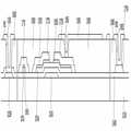
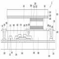
도1은 본 발명의 한 실시예에 따른 전기 영동 표시 장치의 구조를 도시한 배치도이고, 도2는 도1의 전기 영동 표시 장치를 II-II' 선에 따라 자른 단면도이다.FIG. 1 is a layout view illustrating a structure of an electrophoretic display device according to an exemplary embodiment. FIG. 2 is a cross-sectional view of the electrophoretic display device of FIG. 1 taken along line II-II ′.
본 실시예에 따른 전기 영동 표시 장치(1)는 박막 트랜지스터 표시판(100)과 이와 마주보고 있는 공통 전극 표시판(200)을 포함한다.The
먼저, 박막 트랜지스터 표시판(100)에 대해 설명한다.First, the thin film
도1 및 도2에서 보이는 바와 같이, 투명한 유리 등으로 이루어진 절연 기판(110) 위에 게이트 신호를 전달하는 복수의 게이트선(gate line)(121)이 형성되어 있다. 게이트선(121)은 가로 방향으로 뻗어 있으며, 각 게이트선(121)은 복수의 게이트 전극(gate electrode)(124) 및 다른 층이나 외부 회로와의 연결을 위한 넓은 끝부분(129)을 포함한다.As shown in FIGS. 1 and 2, a plurality of
게이트선(121)은 알루미늄과 알루미늄 합금 등 알루미늄 계열의 금속, 은과 은 합금 등 은 계열의 금속, 구리와 구리 합금 등 구리 계열의 금속, 몰리브덴과 몰리브덴 합금 등 몰리브덴 계열의 금속, 크롬, 티타늄, 탄탈륨 따위로 이루어지는 것이 바람직하다. 게이트선(121)은 물리적 성질이 다른 두 개의 막, 즉 하부막(도시하지 않음)과 그 위의 상부막(도시하지 않음)을 포함할 수 있다. 상부막은 게이트선(121)의 신호 지연이나 전압 강하를 줄일 수 있도록 낮은 비저항(resistivity)의 금속, 예를 들면 알루미늄(Al)이나 알루미늄 합금 등 알루미늄 계열의 금속으로 이루어진다. 이와는 달리, 하부막은 다른 물질, 특히 ITO(indium tin oxide) 및 IZO(indium zinc oxide)와의 접촉 특성이 우수한 물질, 이를테면 몰리브덴(Mo), 몰리브덴 합금, 크롬(Cr) 등으로 이루어진다. 하부막과 상부막의 조합의 예로는 크롬/알루미늄-네오디뮴(Nd) 합금을 들 수 있다.The
게이트선(121)은 단일막 구조를 가지거나 세 층 이상을 포함할 수 있다.The
게이트선(121) 위에는 질화규소(SiNx) 따위로 이루어진 게이트 절연막(gate insulating layer)(140)이 형성되어 있다.A
게이트 절연막(140) 상부에는 수소화 비정질 규소(hydrogenated amorphous silicon) 등으로 이루어진 복수의 선형 반도체층(151)이 형성되어 있다. 선형 반도체층(151)은 세로 방향으로 뻗어 있으며, 게이트 전극(124)을 향하여 뻗어 나온 복수의 돌출부(extension)(154)를 포함한다. 또한, 선형 반도체층(151)은 게이트선(121)과 만나는 지점 부근에서 폭이 커져서 게이트선(121)의 넓은 면적을 덮고 있다.A plurality of linear semiconductor layers 151 made of hydrogenated amorphous silicon or the like are formed on the
반도체층(151)의 상부에는 실리사이드(silicide) 또는 n형 불순물이 고농도로 도핑되어 있는 n+ 수소화 비정질 규소 따위의 물질로 이루어진 복수의 선형 및 섬형 저항성 접촉 부재(ohmic contact)(161, 165)가 형성되어 있다. 선형 접촉 부재(161)는 복수의 돌출부(163)를 가지고 있으며, 상기 돌출부(163)와 섬형 접촉 부재(165)는 쌍을 이루어 반도체층(151)의 돌출부(154) 위에 위치한다.A plurality of linear and island ohmic
저항성 접촉 부재(163, 165) 및 게이트 절연막(140) 위에는 각각 복수의 데이터선(data line)(171), 복수의 드레인 전극(drain electrode)(175)이 형성되어 있다.A plurality of
데이터선(171)은 세로 방향으로 뻗어 게이트선(121)과 교차하며 데이터 전압(data voltage)을 전달한다. 각 데이터선(171)은 게이트 전극(124)을 향하여 뻗어 J자형으로 굽은 복수의 소스 전극(source electrode)(173)과 다른 층 또는 외부 구동 회로와의 접속을 위한 넓은 끝부분(179)을 포함한다. 한 쌍의 소스 전극(173)과 드레인 전극(175)은 서로 분리되어 있으며 게이트 전극(124)에 대하여 서로 반대쪽에 위치되어 있다.The
데이터선(171) 및 드레인 전극(175)은 크롬 또는 몰리브덴 계열의 금속, 탄탈륨 및 티타늄 등 내화성 금속으로 이루어지는 것이 바람직하며, 몰리브덴(Mo), 몰리브덴 합금, 크롬(Cr) 따위의 하부막(도시하지 않음)과 그 위에 위치한 알루미늄 계열 금속인 상부막(도시하지 않음)으로 이루어진 다층막 구조를 가질 수 있다.The
게이트 전극(124), 소스 전극(173) 및 드레인 전극(175)은 반도체층(151)의 돌출부(154)와 함께 박막 트랜지스터(Thin Film Transistor, TFT)를 이루며, 박막 트랜지스터의 채널(channel)은 소스 전극(173)과 드레인 전극(175) 사이의 돌출부(154)에 형성되어 있다.The
저항성 접촉 부재(161, 165)는 그 아래의 반도체층(151)과 그 상부의 소스 전극(173) 및 드레인 전극(175) 사이에 존재하며 접촉 저항을 낮추어 주는 역할을 한다.The
선형 반도체층(151)은 소스 전극(173)과 드레인 전극(175) 사이를 비롯하여 데이터선(171) 및 드레인 전극(175)에 가리지 않고 노출된 부분을 가지고 있으며, 대부분의 영역에서 선형 반도체층(151)의 폭이 데이터선(171)의 폭보다 작지만 전술한 바와 같이 게이트선(121)과 만나는 부분에서 폭이 커져서 게이트선(121)과 데이터선(171) 사이의 절연을 강화한다.The
데이터선(171), 드레인 전극(175) 및 노출된 반도체층(151) 위에는 평탄화 특성이 우수하며 감광성(photosensitivity)을 가지는 유기 물질, 플라즈마 화학 기상 증착(Plasma Enhanced Chemical Vapor Deposition, PECVD)으로 형성되는 a- Si:C:O, a-Si:O:F 등의 저유전율 절연 물질, 또는 무기 물질인 질화규소(SiNx) 따위로 이루어진 보호막(passivation layer)(180)이 단일층 또는 복수층으로 형성되어 있다. 예컨대, 유기 물질로 형성하는 경우에는 소스 전극(173)과 드레인 전극(175) 사이의 반도체층(154)이 노출된 부분으로 보호막(180)의 유기 물질이 접촉하는 것을 방지하기 위하여, 유기막의 하부에 질화규소(SiNx) 또는 산화규소(SiO2)로 이루어진 절연막(도시하지 않음)이 추가로 형성될 수도 있다.On the
보호막(180)에는 게이트선(121)의 끝부분(129), 드레인 전극(175) 및 데이터선(171)의 끝부분(179)을 각각 노출시키는 복수의 접촉구(contact hole)(181, 185, 182)가 형성되어 있다.The
보호막(180) 위에는 ITO 또는 IZO로 이루어진 복수의 화소 전극(pixel electrode)(190) 및 복수의 접촉 보조 부재(contact assistant)(81, 82)가 형성되어 있다.A plurality of
화소 전극(190)은 접촉구(185)를 통하여 드레인 전극(175)과 물리적·전기적으로 연결되어 드레인 전극(175)으로부터 데이터 전압을 받는다.The
데이터 전압이 인가된 화소 전극(190)은 공통 전압(common voltage)을 인가 받는 공통 전극 표시판(200)의 공통 전극(220)과 함께 전기장을 생성함으로써 잉크(300)에 분산되어 있는 전기 영동 부재(310)인 전기 영동 입자(314, 315)의 위치를 변화시킴으로써 원하는 색상을 표현한다.The
접촉 보조 부재(81, 82)는 접촉구(181, 182)를 통하여 게이트선(121)의 끝부 분(129) 및 데이터선(171)의 끝부분(179)과 각각 연결된다. 접촉 보조 부재(81, 82)는 게이트선(121) 및 데이터선(171)의 끝부분과 구동 집적 회로와 같은 외부 장치와의 접착성을 보완하고 이들을 보호한다.The
보호막(180) 상부에는 유기 절연 물질 및 무기 절연 물질 중 적어도 어느 하나를 포함하며, 화소 전극(190) 간을 구분하는 격벽(191)이 형성되어 있다. 격벽(191)은 화소 전극(190)의 가장자리 주변을 둘러싸서 전기 영동 부재(310)가 분산되어 있는 잉크(300)가 충진될 영역을 한정한다.The
격벽(191)에 둘러싸인 화소 전극(190) 위의 영역에는 전기 영동 부재(310)가 분산되어 있는 잉크(300)가 충진되어 있다.An
잉크(300)는 화소 전극(190) 위의 영역에 전기 영동 부재(310)를 드로핑하기 위한 드로핑 용매이다. 또한 잉크(300)는 전기 영동 부재(310)가 화소 전극(190) 위의 영역에 드로핑된 후 전기 영동 부재(310)를 화소전극(190)과 공통 전극(220)에 가해지는 전압에 따라 유동하게 하는 분산매이다. 잉크(300)는 본 실시예에서는 투명한 용매를 사용하고 있다.The
잉크(300)에 분산되어 있는 전기 영동 부재(310)는 제1 전기 영동 입자(314)와 제2 전기 영동 입자(315)를 포함하고 있다.The
제1 전기 영동 입자(314)는 음의 전하를 띄는 대전 입자로서 적색, 녹색 및 청색 중 어느 하나의 색을 가지거나 또는 옐로(yellow), 마젠타(magenta), 시안(cyan) 중 어느 하나의 색을 가진다. 적색, 녹색 및 청색 또는 옐로(yellow), 마젠타(magenta), 시안(cyan) 중 어느 하나의 색을 갖는 각 제1 전기 영동 입 자(314)는 복수의 화소 전극(190) 위의 영역에 순서대로 반복적으로 배치되어 있다.The first
제2 전기 영동 입자(315)는 검은색을 가지며, 양의 전하를 띄는 대전 입자이다.The second
제1 전기 영동 입자(314) 및 제2 전기 영동 입자(315)는 상기와 반대로 각각 양의 전하와 음의 전하를 띌 수도 있다.The first
다음으로 박막 트랜지스터 표시판(100)에 대향 배치되어 있는 공통 전극 표시판(200)에 대해 설명한다.Next, the common
공통 전극 표시판(200)은 격벽(191)에 둘러싸인 화소 전극(190) 위의 영역에 충진되어 있는 잉크(300)가 외부로 누출되지 않도록 격벽(191)에 완전히 밀착되어 있다. 공통 전극 표시판(200)은 절연 기판(210)과 절연 기판(210) 위에 균일한 두께로 형성되어 있는 공통 전극(270)을 포함한다.The common
공통 전극(270)은 ITO 또는 IZO 이루어진 투명 전극으로서 전기 영동 부재(310)에 공통 전압을 인가한다.The common electrode 270 is a transparent electrode made of ITO or IZO and applies a common voltage to the
이하에서는 본 발명의 한 실시예에 따른 전기 영동 표시 장치(1)가 여러 가지 색상의 화상을 표시하는 방법에 대해 설명한다.Hereinafter, a method of displaying an image of various colors by the
전기 영동 표시 장치(1)의 드레인 전극(175)을 통해 화소 전극(190)에 음의 전압이 인가되고 공통 전극(220)에 양의 전압이 인가되는 경우를 설명한다.A case in which a negative voltage is applied to the
이 경우 잉크(300)에 불규칙하게 분산되어 있으며 음 전하를 띄는 제1 전기 영동 입자(314)는 양의 전압이 인가된 공통 전극(220)으로 이동하여 배열하게 된 다. 한편, 양 전하를 띄는 제2 전기 영동 입자(315)는 음의 전압이 인가된 화소 전극(190)으로 이동하여 배열하게 된다. 배열이 이루어지면 공통 전극 표시판(200)을 통과하여 입사된 외부광은 제1 전기 영동 입자(314)에 반사되면서 각 화소 영역 별로 전기 영동 입자(314)가 갖는 색을 외부로 표시하게 된다.In this case, the first
다음으로 전기 영동 표시 장치(1)의 드레인 전극(175)을 통해 화소 전극(190)에 양의 전압이 인가되고 공통 전극(220)에 음의 전압이 인가되는 경우를 설명한다.Next, a case in which a positive voltage is applied to the
이 경우 잉크(300)에 불규칙하게 분산되어 있으며 음 전하를 띄는 제1 전기 영동 입자(314)는 양의 전압이 인가된 화소 전극(190)으로 이동하여 배열하게 된다. 한편, 양 전하를 띄는 제2 전기 영동 입자(315)는 음의 전압이 인가된 공통 전극(220)으로 이동하여 배열하게 된다.In this case, the first
이로 인해 외부로부터 공통 전극 표시판(200)을 가로질러 입사된 외부광은 검은색을 갖는 제2전기 영동 입자(314)에 반사되면서 외부로 검은색을 표시하게 된다.As a result, the external light incident from the outside across the common
본 발명의 한 실시예에 따른 전기 영동 표시 장치(1)에 따르면, 화소 전극(190) 간을 구획하는 격벽(191)을 형성함으로써 전기 영동 부재(310)을 분산시킨 잉크(300)를 드로핑에 의한 간편한 방법으로 화소 전극(190) 위의 영역에 충진 할 수 있다. 따라서 화소 전극(190) 상의 전기 영동 부재(310)를 용이하면서도 정확하게 배치할 수 있어 제조 효율 및 표시 성능을 향상할 수 있다. 또한 전기 영동 입자 및 분산매를 가두는 캡슐을 별도로 제조할 필요가 없기 때문에 제조 효율을 더욱 향상시킬 수 있다.According to the
이하에서는 본 발명의 한 실시예에 따른 전기 영동 표시 장치(1)의 제조 방법에 대하여 도1 및 도2, 도3a 내지 도3g를 참조하여 상세히 설명한다.Hereinafter, a method of manufacturing the
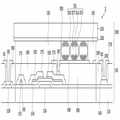
도3a 내지 도3g는 본 발명의 한 실시예에 따른 전기 영동 표시 장치의 제조 방법을 순차적으로 도시한 단면도이다.3A to 3G are cross-sectional views sequentially illustrating a method of manufacturing an electrophoretic display device according to an exemplary embodiment of the present invention.
먼저, 절연 기판(110) 위에 스퍼터링(sputtering) 등의 방법으로 알루미늄과 알루미늄 합금 등 알루미늄 계열의 금속, 은과 은 합금 등 은 계열의 금속, 구리와 구리 합금 등 구리 계열의 금속, 몰리브덴과 몰리브덴 합금 등 몰리브덴 계열의 금속, 크롬, 티타늄, 탄탈륨 등으로 이루어진 도전막을 형성한다.First, aluminum-based metals such as aluminum and aluminum alloys, silver-based metals such as silver and silver alloys, copper-based metals such as copper and copper alloys, molybdenum and molybdenum alloys on the insulating
이후 도 3a에 도시한 바와 같이 사진 식각 공정으로 도전막을 식각하여 복수의 게이트 전극(124) 및 외부회로와 연결하기 위한 게이트선의 끝부분(129)을 포함하는 복수의 게이트선(121)을 형성한다.Thereafter, as illustrated in FIG. 3A, the conductive layer is etched by a photolithography process to form a plurality of
다음 도3b에 도시한 바와 같이, 게이트선(121)을 덮도록 LPCVD(low temperature chemical vapor deposition), PECVE(plasma enhanced chemical vapor deposition)의 방법으로 게이트 절연막(140), 수소화 비정질 규소막, N+가 도핑된 비정질 규소막을 차례로 적층하고, 수소화 비정질 규소막, N+가 도핑된 비정질 규소막을 패터닝하여 복수의 돌출부(154)를 포함하는 선형 반도체층(151) 및 복수의 저항성 접촉 패턴(164)을 형성한다. 게이트 절연막(140)은 질화규소 따위로 형성한다.Next, as shown in FIG. 3B, the
다음 크롬 또는 몰리브덴 계열의 금속, 탄탈륨 및 티타늄 등 내화성 금속으 로 이루어진 도전막을 스퍼터링 따위로 적층한다.Next, a conductive film made of refractory metals such as chromium or molybdenum-based metals, tantalum and titanium is laminated by sputtering.
이후 도3c에 도시한 바와 같이, 사진 식각 공정으로 도전막을 식각하여 복수의 소스 전극(173) 및 데이터선의 끝부분(179)를 포함하는 데이터선(171)과 복수의 드레인 전극(175)을 형성한다.3C, the conductive layer is etched by a photolithography process to form the
그러고 데이터선(171) 및 드레인 전극(175)으로 가려지지 않은 저항성 접촉 패턴(164) 부분을 제거하여, 저항성 접촉 패턴(164)을 두 개의 저항성 접촉 부재(163, 165)로 분리하는 한편, 둘 사이의 반도체층(154) 부분을 노출시킨다. 이어, 노출된 반도체층(154)의 표면을 안정화시키기 위하여 산소 플라스마를 실시하는 것이 바람직하다.Then, the portion of the ohmic contact pattern 164 that is not covered by the
다음으로, 도 3d에 도시한 바와 같이, 평탄화 특성이 우수하며 감광성을 가지는 유기물질, 플라즈마 화학 기상 증착(PECVD)으로 형성되는 a-Si:C:O, a-Si:O:F 등의 저유전율 절연물질, 또는 무기물질인 질화규소(SiNx) 따위를 단일층 또는 복수층으로 형성하여 보호막(passivation layer)(180)을 형성한다.Next, as shown in FIG. 3D, organic materials having excellent planarization characteristics and photosensitivity, such as a-Si: C: O and a-Si: O: F formed by plasma chemical vapor deposition (PECVD), may be used. A
그 다음, 보호막(180) 위에 포토 레지스트를 도포한 후 광마스크를 통하여 포토 레지스트를 노광 현상하여 포토 레지스트 패턴을 형성한 후 포토 레지스트 패턴을 이용한 사진 식각 공정으로 보호막(180) 및 게이트 절연막(140)을 패터닝하여 복수의 접촉구(181, 185, 182)를 형성한다.Next, after the photoresist is applied on the
그 다음, 도 3e에 도시한 바와 같이, 보호막(180) 위에 ITO 또는 IZO를 스퍼터링으로 적층하고 사진 식각 공정으로 복수의 화소 전극(190)과 복수의 접촉 보조 부재(81, 82)를 형성한다.Next, as illustrated in FIG. 3E, ITO or IZO is stacked on the
그 다음, 도3f에 도시한 바와 같이, 보호막(180) 및 화소 전극(190) 상에 유기 절연 물질 및 무기 절연 물질 중 적어도 어느 하나를 포함하는 격벽 물질을 형성한다. 이 후 사진 식각 공정을 통한 패터닝을 통해 화소 전극(190) 간을 구분하며 화소 전극(190) 위의 영역을 드러내는 격자 모양의 격벽(191)을 형성한다.3F, a barrier material including at least one of an organic insulating material and an inorganic insulating material is formed on the
이 후 도3g에서 보는 바와 같이 젯팅 부재(10)를 이용하여 격벽(191) 사이에 노출된 화소 전극(190) 위에 전기 영동 부재(310)가 분산되어 있는 잉크(300)를 드로핑하여 격벽(191)에 의해 정의된 화소 전극(190) 위의 영역을 충진한다.Thereafter, as shown in FIG. 3G, the
그런 다음 공통 전극(220)이 형성되어 있는 공통 전극 표시판(200)을 마련하여 박막 트랜지스터 표시판(100)의 격벽(191)에 밀착시키면 도2에 도시한 전기 영동 표시 장치(1)가 완성된다.Then, the common
본 발명의 한 실시예에 따른 전기 영동 표시 장치(1)의 제조 방법에 의하면, 화소 전극(190) 간을 구획하는 격벽(191)을 형성함으로써 젯팅 부재(10)를 이용하여 간편하게 화소 전극(190) 위의 영역에 전기 영동 부재(310)를 위치시킬 수 있다. 따라서 화소 전극(190) 위에 전기 영동 부재(310)를 용이하면서도 정확하게 위치시킬 수 있어 제조 효율 및 표시 성능을 향상할 수 있다.According to the manufacturing method of the
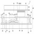
이하에서는 본 발명의 다른 실시예에 따른 전기 영동 표시 장치(2)를 도4를 참조하여 설명한다. 도4는 본 발명의 다른 실시예에 따른 전기 영동 표시 장치의 단면도이다.Hereinafter, an electrophoretic display device 2 according to another exemplary embodiment of the present invention will be described with reference to FIG. 4. 4 is a cross-sectional view of an electrophoretic display device according to another exemplary embodiment of the present invention.
본 발명의 다른 실시예에 따른 전기 영동 표시 장치(2)는 공통 전극 표시판(201)이 공통 전극(220) 위에 형성된 유기막(230)을 더 포함하고 있는 것을 제외 하고는 도1 및 2에 도시한 본 발명의 한 실시예에 따른 전기 영동 표시 장치(1)와 동일하다.The electrophoretic display 2 according to another exemplary embodiment of the present invention is illustrated in FIGS. 1 and 2 except that the common
본 발명의 다른 실시예에 따른 전기 영동 표시 장치(2)에 의하면 공통 전극(220) 위에 유기막(230)을 더 형성함으로써 공통전극 표시판(201)과 격벽(191)과의 밀착력을 더 높일 수 있다.According to the electrophoretic display 2 according to another exemplary embodiment of the present invention, the organic layer 230 is further formed on the
이하에서는 본 발명의 다른 실시예에 따른 전기 영동 표시 장치(3)를 도5를 참조하여 설명한다. 도5는 본 발명의 다른 실시예에 따른 전기 영동 표시 장치의 단면도이다.Hereinafter, an electrophoretic display 3 according to another exemplary embodiment of the present invention will be described with reference to FIG. 5. 5 is a cross-sectional view of an electrophoretic display device according to another exemplary embodiment of the present invention.
본 발명의 다른 실시예에 따른 전기 영동 표시 장치(3)는 도1 및 도2에 도시한 본 발명의 한 실시예에 따른 전기 영동 표시 장치(1)와 달리 박막 트랜지스터 표시판(101)의 잉크(300)에 분산되어 있는 전기 영동 부재(311)가 제1 전기 영동 입자(314) 및 제2 전기 영동 입자(315)가 분산되어 있는 투명한 분산매(317)와 이들을 가두고 있는 캡슐(319)을 더 포함하고 있다.The electrophoretic display device 3 according to another exemplary embodiment of the present invention is different from the
이러한 구성의 차이를 보이는 이유는 젯팅 부재(10)를 통해 잉크(300)와 함께 드로핑되는 전기 영동 부재(311)가 전기 영동 입자(314, 315)만으로 구성될 수도 있으나, 전기 영동 입자(314, 315)와 전기 영동 입자(314, 315)가 분산되어 있는 투명한 분산매(317)를 내부에 포함하는 캡슐(319)로 구성될 수도 있기 때문이다.The reason for the difference in this configuration is that the
이하에서는 본 발명의 다른 실시예에 따른 전기 영동 표시 장치(4)를 도6을 참조하여 설명한다. 도6은 본 발명의 다른 실시예에 따른 전기 영동 표시 장치의 단면도이다.Hereinafter, an electrophoretic display 4 according to another exemplary embodiment of the present invention will be described with reference to FIG. 6. 6 is a cross-sectional view of an electrophoretic display device according to another exemplary embodiment of the present invention.
본 발명의 다른 실시예에 따른 전기 영동 표시 장치(4)는 도1 및 도2에 도시한 본 발명의 한 실시예에 따른 전기 영동 표시 장치(1)와 달리 전기 영동 부재(312)가 음의 전하를 띄는 대전 입자로서 적색, 녹색 및 청색 중 어느 하나의 색을 가지거나 또는 옐로(yellow), 마젠타(magenta), 시안(cyan) 중 어느 하나의 색을 가지는 한 종류의 전기 영동 입자(314)만으로 구성되어 있다. 또한 잉크(300)는 투명이 아니라 검은색을 갖도록 구성되어 있다.In the electrophoretic display device 4 according to another exemplary embodiment of the present invention, unlike the
본 발명의 다른 실시예에 따른 전기 영동 표시 장치(4)는 전기 영동 입자(314)가 갖는 색상을 표시하기 위해서 화소 전극(190)에 음의 전압을 인가하고 공통 전극(220)에 양의 전압을 인가하여 음 전하를 띄는 전기 영동 입자(314)가 공통 전극(220)으로 이동하여 배열되도록 한다. 한편, 검은 색을 표시하기 위해서는 화소 전극(190)에 양의 전압의 인가하고 공통 전극(220)에 음의 전압을 인가하여 음 전하를 띄는 전기 영동 입자(314)가 화소 전극(190)으로 이동하여 배열되도록 한다. 이를 통해 외부광이 검은색을 갖는 잉크(300)로 입사된 후 다시 반사되어 나가게 되어 검은색 화상이 표시 되게 된다.The electrophoretic display 4 according to another exemplary embodiment of the present invention applies a negative voltage to the
전기 영동 입자(314)는 양 전하를 띌 수도 있으며 이 경우 색상 표현을 위해서 화소 전극(190)과 공통 전극(220)에 인가되는 전압을 상기와 반대로 인가하면 된다.The
이하에서는 본 발명의 다른 실시예에 따른 전기 영동 표시 장치(5)를 도7을 참조하여 설명한다. 도7은 본 발명의 다른 실시예에 따른 전기 영동 표시 장치의 단면도이다.Hereinafter, an electrophoretic display 5 according to another exemplary embodiment of the present invention will be described with reference to FIG. 7. 7 is a cross-sectional view of an electrophoretic display device according to another exemplary embodiment of the present invention.
본 발명의 다른 실시예에 따른 전기 영동 표시 장치(5)는 도5에 도시한 본 발명의 다른 실시예에 따른 전기 영동 표시 장치(3)와 달리 분산매(318)에 분산된 전기 영동 입자(314)가 한 종류만으로 구성되어 있다. 또한 분산매(318)는 검은색을 갖도록 구성되어 있다. 여기서, 전기 영동 입자(314)는 음의 전하를 띄는 대전 입자로서 적색, 녹색 및 청색 중 어느 하나의 색을 가지거나 또는 옐로(yellow), 마젠타(magenta), 시안(cyan) 중 어느 하나의 색을 갖는다.Electrophoretic display device 5 according to another embodiment of the present invention is
본 발명의 다른 실시예에 따른 전기 영동 표시 장치(5)는 전기 영동 입자(314)가 갖는 각 색상을 표시하기 위해서는 화소 전극(190)에 음의 전압을 인가하고 공통 전극(220)에 양의 전압을 인가하여 음 전하를 띄는 전기 영동 입자(314)가 공통 전극(220)으로 이동하여 배열되도록 한다. 한편, 검은색을 표시하기 위해서는 화소 전극(190)에 양의 전압을 인가하고 공통 전극(220)에 음의 전압을 인가하여 음 전하를 띄는 전기 영동 입자(314)가 화소 전극(190)으로 이동하여 배열되도록 한다. 이를 통해 외부광이 검은색을 갖는 분산매(318)로 입사된 후 다시 반사되어 나가게 되어 검은색 화상이 표시 되게 된다.In order to display each color of the
전기 영동 입자(314)는 양 전하를 띌 수도 있으며 이 경우 색상 표현을 위해서 화소 전극(190)과 공통 전극(220)에 인가되는 전압을 상기와 반대로 인가하면 된다.The
도4 내지 도7에 도시한 본 발명의 다른 실시예들에 따른 전기 영동 표시 장치(2, 3, 4, 5)에 의해서도 화소 전극(190) 간을 구획하는 격벽(191)을 형성함으로 써 잉크젯 프린팅 등의 방법을 이용하여 간편하게 화소 전극(190) 위의 영역에 전기 영동 부재(311, 312, 313)를 위치시킬 수 있다. 따라서 화소 전극(190) 위에 전기 영동 부재(311, 312, 313)를 용이하면서도 정확하게 배치할 수 있어 제조 효율 및 표시 성능을 향상할 수 있다.The inkjet is formed by forming the
이상에서 본 발명의 바람직한 실시예에 대하여 상세하게 설명하였지만 본 발명의 권리범위는 이에 한정되는 것은 아니고 다음의 청구범위에서 정의하고 있는 본 발명의 기본 개념을 이용한 당업자의 여러 변형 및 개량 형태 또한 본 발명의 권리범위에 속하는 것이다.Although the preferred embodiments of the present invention have been described in detail above, the scope of the present invention is not limited thereto, and various modifications and improvements of those skilled in the art using the basic concepts of the present invention defined in the following claims are also provided. It belongs to the scope of rights.
이상과 같이, 본 발명에 의하면, 용이하면서도 정밀한 방법으로 제조되어 제조 효율과 표시 성능이 우수한 전기 영동 표시 장치 및 그 제조방법이 제공된다.As described above, the present invention provides an electrophoretic display device manufactured by an easy and precise method and excellent in manufacturing efficiency and display performance, and a manufacturing method thereof.
Claims (30)
Translated fromKoreanPriority Applications (5)
| Application Number | Priority Date | Filing Date | Title |
|---|---|---|---|
| KR1020060056435AKR20070121403A (en) | 2006-06-22 | 2006-06-22 | Electrophoretic display device and manufacturing method thereof |
| US11/552,345US7436578B2 (en) | 2006-06-22 | 2006-10-24 | Electrophoretic display and manufacturing method thereof |
| CNA2006101470476ACN101093335A (en) | 2006-06-22 | 2006-11-13 | Electrophoretic display and manufacturing method thereof |
| EP07008172AEP1870769A1 (en) | 2006-06-22 | 2007-04-21 | Electrophoretic display and manufacturing method thereof |
| JP2007161514AJP2008003598A (en) | 2006-06-22 | 2007-06-19 | Electrophoretic display device and manufacturing method thereof |
Applications Claiming Priority (1)
| Application Number | Priority Date | Filing Date | Title |
|---|---|---|---|
| KR1020060056435AKR20070121403A (en) | 2006-06-22 | 2006-06-22 | Electrophoretic display device and manufacturing method thereof |
Publications (1)
| Publication Number | Publication Date |
|---|---|
| KR20070121403Atrue KR20070121403A (en) | 2007-12-27 |
Family
ID=38010261
Family Applications (1)
| Application Number | Title | Priority Date | Filing Date |
|---|---|---|---|
| KR1020060056435AWithdrawnKR20070121403A (en) | 2006-06-22 | 2006-06-22 | Electrophoretic display device and manufacturing method thereof |
Country Status (5)
| Country | Link |
|---|---|
| US (1) | US7436578B2 (en) |
| EP (1) | EP1870769A1 (en) |
| JP (1) | JP2008003598A (en) |
| KR (1) | KR20070121403A (en) |
| CN (1) | CN101093335A (en) |
Cited By (4)
| Publication number | Priority date | Publication date | Assignee | Title |
|---|---|---|---|---|
| KR20110074245A (en)* | 2009-12-24 | 2011-06-30 | 엘지디스플레이 주식회사 | Electrophoretic display device and manufacturing method thereof |
| US8441711B2 (en) | 2008-09-23 | 2013-05-14 | Lg Display Co., Ltd. | Electrophoretic display device and method of fabricating the same |
| KR101285638B1 (en)* | 2008-09-23 | 2013-07-12 | 엘지디스플레이 주식회사 | Electrophoretic display device and method of fabricating the same |
| CN115116403A (en)* | 2022-08-29 | 2022-09-27 | 惠科股份有限公司 | E-ink screen and control method, device and computer-readable storage medium thereof |
Families Citing this family (13)
| Publication number | Priority date | Publication date | Assignee | Title |
|---|---|---|---|---|
| KR101362035B1 (en)* | 2007-05-09 | 2014-02-11 | 엘지디스플레이 주식회사 | method for manufacturing flexible display substrate |
| JP5371341B2 (en)* | 2007-09-21 | 2013-12-18 | 株式会社半導体エネルギー研究所 | Electrophoretic display device |
| KR100936874B1 (en)* | 2007-12-18 | 2010-01-14 | 삼성모바일디스플레이주식회사 | Method for manufacturing thin film transistor and method for manufacturing organic light emitting display device comprising thin film transistor |
| KR20100138762A (en)* | 2009-06-24 | 2010-12-31 | 가시오게산키 가부시키가이샤 | Electrophoretic display |
| US20110090143A1 (en)* | 2009-10-20 | 2011-04-21 | Seung-Han Paek | Electrophoretic display device and fabrication method thereof |
| CN101699343B (en)* | 2009-11-09 | 2012-01-25 | 友达光电股份有限公司 | Electrophoretic display pixel and display device |
| US8638492B2 (en)* | 2010-01-12 | 2014-01-28 | Delta Electronics, Inc. | Display cell, display apparatus and method for making same |
| TWI461809B (en)* | 2010-07-06 | 2014-11-21 | Lg Display Co Ltd | Electrophoretic display device and method of manufacturing same |
| TWI457679B (en)* | 2011-06-03 | 2014-10-21 | E Ink Holdings Inc | Electrophoretic display |
| US8804228B1 (en)* | 2012-12-28 | 2014-08-12 | Google Inc. | Thermal regulation of balloon payload using electronic ink |
| JP5765369B2 (en)* | 2013-05-22 | 2015-08-19 | 大日本印刷株式会社 | Reflective display device |
| CN109115625A (en)* | 2018-10-08 | 2019-01-01 | 西南石油大学 | A kind of shale hydration dynamic changes of strength variation test new equipment |
| KR102781957B1 (en)* | 2020-07-07 | 2025-03-18 | 삼성전자주식회사 | Display module and method for manufacturing thereof |
Family Cites Families (17)
| Publication number | Priority date | Publication date | Assignee | Title |
|---|---|---|---|---|
| JP4058785B2 (en) | 1997-11-26 | 2008-03-12 | ブラザー工業株式会社 | Rewritable seat |
| EP1557714B1 (en) | 1998-04-10 | 2013-11-06 | E Ink Corporation | Full color reflective display with multichromatic sub-pixels |
| JP4385438B2 (en) | 1999-05-14 | 2009-12-16 | ブラザー工業株式会社 | Recording medium, electrophoretic display device, and control method of recording medium |
| US6545797B2 (en) | 2001-06-11 | 2003-04-08 | Sipix Imaging, Inc. | Process for imagewise opening and filling color display components and color displays manufactured thereof |
| JP4006925B2 (en)* | 2000-05-30 | 2007-11-14 | セイコーエプソン株式会社 | Method for manufacturing electrophoretic display device |
| JP3805180B2 (en)* | 2000-09-14 | 2006-08-02 | 株式会社東芝 | Display element |
| TW550529B (en) | 2001-08-17 | 2003-09-01 | Sipix Imaging Inc | An improved electrophoretic display with dual-mode switching |
| EP1478973B1 (en)* | 2002-02-19 | 2008-07-23 | Koninklijke Philips Electronics N.V. | Electrophoretic display device |
| KR100482472B1 (en) | 2002-02-20 | 2005-04-14 | 비오이 하이디스 테크놀로지 주식회사 | Apparatus for electrophoretic display and method for manufacturing the same |
| JP2003315845A (en) | 2002-04-22 | 2003-11-06 | Toppan Printing Co Ltd | Electrophoretic display panel and method of manufacturing the same |
| JP4154175B2 (en) | 2002-05-31 | 2008-09-24 | キヤノン株式会社 | Method for manufacturing electrophoretic display element |
| JP2004170903A (en)* | 2002-10-31 | 2004-06-17 | Canon Inc | Electrophoretic display |
| JP4125096B2 (en) | 2002-11-15 | 2008-07-23 | キヤノン株式会社 | Method for manufacturing electrophoretic display device |
| KR100951351B1 (en)* | 2003-04-22 | 2010-04-08 | 삼성전자주식회사 | Thin film transistor array panel and electrophoretic display device including the same |
| KR20050000680A (en) | 2003-06-24 | 2005-01-06 | 엘지.필립스 엘시디 주식회사 | In Plain Electrophoretic Display Device |
| JP2005107466A (en) | 2003-09-29 | 2005-04-21 | Takeshi Aoki | Electrophoretic and magnetophoretic display device in which one microcapsule is capable of displaying four or five colors |
| KR101133759B1 (en)* | 2004-12-28 | 2012-04-09 | 삼성전자주식회사 | Electrophoretic indication Display and Method for Manufacturing the same |
- 2006
- 2006-06-22KRKR1020060056435Apatent/KR20070121403A/ennot_activeWithdrawn
- 2006-10-24USUS11/552,345patent/US7436578B2/enactiveActive
- 2006-11-13CNCNA2006101470476Apatent/CN101093335A/enactivePending
- 2007
- 2007-04-21EPEP07008172Apatent/EP1870769A1/ennot_activeWithdrawn
- 2007-06-19JPJP2007161514Apatent/JP2008003598A/enactivePending
Cited By (5)
| Publication number | Priority date | Publication date | Assignee | Title |
|---|---|---|---|---|
| US8441711B2 (en) | 2008-09-23 | 2013-05-14 | Lg Display Co., Ltd. | Electrophoretic display device and method of fabricating the same |
| KR101285638B1 (en)* | 2008-09-23 | 2013-07-12 | 엘지디스플레이 주식회사 | Electrophoretic display device and method of fabricating the same |
| KR20110074245A (en)* | 2009-12-24 | 2011-06-30 | 엘지디스플레이 주식회사 | Electrophoretic display device and manufacturing method thereof |
| CN115116403A (en)* | 2022-08-29 | 2022-09-27 | 惠科股份有限公司 | E-ink screen and control method, device and computer-readable storage medium thereof |
| US12142234B2 (en) | 2022-08-29 | 2024-11-12 | HKC Corporation Limited | Electronic ink screen and control method therefor and control device therefor |
Also Published As
| Publication number | Publication date |
|---|---|
| US7436578B2 (en) | 2008-10-14 |
| CN101093335A (en) | 2007-12-26 |
| US20070297039A1 (en) | 2007-12-27 |
| EP1870769A1 (en) | 2007-12-26 |
| JP2008003598A (en) | 2008-01-10 |
Similar Documents
| Publication | Publication Date | Title |
|---|---|---|
| KR20070121403A (en) | Electrophoretic display device and manufacturing method thereof | |
| US8884303B2 (en) | TFT substrate including a data insulating layer with contact hole overlapping channel region | |
| KR101374890B1 (en) | Method for driving electrophoretic display | |
| KR101720524B1 (en) | Liquid Crystal Display Device and Method for manufacturing the same | |
| US8729612B2 (en) | Active matrix substrate and method for manufacturing the same | |
| KR20080023913A (en) | Electrophoretic display device and driving method thereof | |
| CN207265054U (en) | A kind of array base palte, display panel and display device | |
| JP2006293312A (en) | Electrophoretic display device | |
| KR20120053295A (en) | Thin film transistor array panel and display device including the same, and manufacturing method thereof | |
| KR20080110347A (en) | Electrophoretic display device and manufacturing method thereof | |
| US7858986B2 (en) | Thin film transistor array panel and method for manufacturing the same | |
| KR20160128518A (en) | Display device and manufacturing method thereof | |
| KR101337255B1 (en) | Electrophoretic display and method for manufacturing thereof | |
| US20160349583A1 (en) | Display device | |
| KR20120077563A (en) | Array substrate and manufacturing method for array substrate | |
| US9915844B2 (en) | Liquid crystal display and method of manufacturing the same | |
| KR20100116006A (en) | Thin film transistor substrate and method of fabricating the same | |
| KR20080023907A (en) | Electrophoretic display device and manufacturing method thereof | |
| KR20080073573A (en) | Liquid crystal panel and its manufacturing method | |
| KR20080046960A (en) | Electrophoretic display device and manufacturing method thereof | |
| KR20080047672A (en) | Electrophoretic display device and manufacturing method thereof | |
| KR20190128023A (en) | Display device and manufacturing method thereof | |
| KR20080068348A (en) | Manufacturing method of display device | |
| KR20080014384A (en) | Electrophoresis display | |
| JP2010114160A (en) | Semiconductor element, method of manufacturing the same, and display device |
Legal Events
| Date | Code | Title | Description |
|---|---|---|---|
| PA0109 | Patent application | Patent event code:PA01091R01D Comment text:Patent Application Patent event date:20060622 | |
| PG1501 | Laying open of application | ||
| PC1203 | Withdrawal of no request for examination | ||
| WITN | Application deemed withdrawn, e.g. because no request for examination was filed or no examination fee was paid |