KR20070117788A - Display substrate, manufacturing method thereof and display device having same - Google Patents
Display substrate, manufacturing method thereof and display device having sameDownload PDFInfo
- Publication number
- KR20070117788A KR20070117788AKR1020060051867AKR20060051867AKR20070117788AKR 20070117788 AKR20070117788 AKR 20070117788AKR 1020060051867 AKR1020060051867 AKR 1020060051867AKR 20060051867 AKR20060051867 AKR 20060051867AKR 20070117788 AKR20070117788 AKR 20070117788A
- Authority
- KR
- South Korea
- Prior art keywords
- layer
- pixel
- electrode
- inorganic insulating
- organic
- Prior art date
- Legal status (The legal status is an assumption and is not a legal conclusion. Google has not performed a legal analysis and makes no representation as to the accuracy of the status listed.)
- Withdrawn
Links
Images


Classifications
- G—PHYSICS
- G02—OPTICS
- G02F—OPTICAL DEVICES OR ARRANGEMENTS FOR THE CONTROL OF LIGHT BY MODIFICATION OF THE OPTICAL PROPERTIES OF THE MEDIA OF THE ELEMENTS INVOLVED THEREIN; NON-LINEAR OPTICS; FREQUENCY-CHANGING OF LIGHT; OPTICAL LOGIC ELEMENTS; OPTICAL ANALOGUE/DIGITAL CONVERTERS
- G02F1/00—Devices or arrangements for the control of the intensity, colour, phase, polarisation or direction of light arriving from an independent light source, e.g. switching, gating or modulating; Non-linear optics
- G02F1/01—Devices or arrangements for the control of the intensity, colour, phase, polarisation or direction of light arriving from an independent light source, e.g. switching, gating or modulating; Non-linear optics for the control of the intensity, phase, polarisation or colour
- G02F1/13—Devices or arrangements for the control of the intensity, colour, phase, polarisation or direction of light arriving from an independent light source, e.g. switching, gating or modulating; Non-linear optics for the control of the intensity, phase, polarisation or colour based on liquid crystals, e.g. single liquid crystal display cells
- G02F1/133—Constructional arrangements; Operation of liquid crystal cells; Circuit arrangements
- G02F1/136—Liquid crystal cells structurally associated with a semi-conducting layer or substrate, e.g. cells forming part of an integrated circuit
- G—PHYSICS
- G02—OPTICS
- G02F—OPTICAL DEVICES OR ARRANGEMENTS FOR THE CONTROL OF LIGHT BY MODIFICATION OF THE OPTICAL PROPERTIES OF THE MEDIA OF THE ELEMENTS INVOLVED THEREIN; NON-LINEAR OPTICS; FREQUENCY-CHANGING OF LIGHT; OPTICAL LOGIC ELEMENTS; OPTICAL ANALOGUE/DIGITAL CONVERTERS
- G02F1/00—Devices or arrangements for the control of the intensity, colour, phase, polarisation or direction of light arriving from an independent light source, e.g. switching, gating or modulating; Non-linear optics
- G02F1/01—Devices or arrangements for the control of the intensity, colour, phase, polarisation or direction of light arriving from an independent light source, e.g. switching, gating or modulating; Non-linear optics for the control of the intensity, phase, polarisation or colour
- G02F1/13—Devices or arrangements for the control of the intensity, colour, phase, polarisation or direction of light arriving from an independent light source, e.g. switching, gating or modulating; Non-linear optics for the control of the intensity, phase, polarisation or colour based on liquid crystals, e.g. single liquid crystal display cells
- G02F1/133—Constructional arrangements; Operation of liquid crystal cells; Circuit arrangements
- G02F1/1333—Constructional arrangements; Manufacturing methods
- G02F1/1335—Structural association of cells with optical devices, e.g. polarisers or reflectors
- G02F1/133509—Filters, e.g. light shielding masks
- G02F1/133514—Colour filters
- H—ELECTRICITY
- H10—SEMICONDUCTOR DEVICES; ELECTRIC SOLID-STATE DEVICES NOT OTHERWISE PROVIDED FOR
- H10D—INORGANIC ELECTRIC SEMICONDUCTOR DEVICES
- H10D30/00—Field-effect transistors [FET]
- H10D30/60—Insulated-gate field-effect transistors [IGFET]
- H10D30/67—Thin-film transistors [TFT]
Landscapes
- Physics & Mathematics (AREA)
- Nonlinear Science (AREA)
- Mathematical Physics (AREA)
- Chemical & Material Sciences (AREA)
- Crystallography & Structural Chemistry (AREA)
- General Physics & Mathematics (AREA)
- Optics & Photonics (AREA)
- Engineering & Computer Science (AREA)
- Microelectronics & Electronic Packaging (AREA)
- Liquid Crystal (AREA)
Abstract
Translated fromKoreanDescription
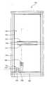
Translated fromKorean도 1은 본 발명의 일 실시예에 따른 표시 기판을 나타낸 평면도이다.1 is a plan view illustrating a display substrate according to an exemplary embodiment of the present invention.
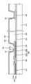
도 2는 도 1의 Ⅰ-Ⅰ'선을 따라 절단한 단면도이다.FIG. 2 is a cross-sectional view taken along the line II ′ of FIG. 1.
도 3은 본 발명의 다른 실시예에 따른 표시 기판을 나타낸 평면도이다.3 is a plan view illustrating a display substrate according to another exemplary embodiment of the present invention.
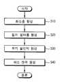
도 4는 본 발명의 일 실시예에 따른 표시 기판의 제조 방법을 나타낸 흐름도이다.4 is a flowchart illustrating a method of manufacturing a display substrate according to an exemplary embodiment of the present invention.
도 5 내지 도 9는 도 4에 도시된 표시 기판의 제조 과정을 나타낸 공정도들이다.5 through 9 are process diagrams illustrating a manufacturing process of the display substrate illustrated in FIG. 4.
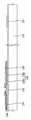
도 10은 본 발명의 일 실시예에 따른 표시 장치를 나타낸 단면도이다.10 is a cross-sectional view illustrating a display device according to an exemplary embodiment of the present invention.
<도면의 주요 부분에 대한 부호의 설명><Explanation of symbols for the main parts of the drawings>
100 : 표시 기판 200 : 화소층100
220 : 화소부230 : 박막 트랜지스터층220: pixel portion 230: thin film transistor layer
231 : 스토리지 전극234 : 게이트 절연막231: storage electrode 234: gate insulating film
240 : 보호막300 : 유기막240: protective film 300: organic film
400 : 무기절연막500 : 화소 전극400: inorganic insulating film 500: pixel electrode
700 : 대향 기판720 : 공통 전극700: opposing substrate 720: common electrode
본 발명은 표시 기판, 이의 제조 방법 및 이를 갖는 표시 장치에 관한 것으로, 더욱 상세하게는 잔상 등의 표시 불량을 방지할 수 있는 표시 기판, 이의 제조 방법 및 이를 갖는 표시 장치에 관한 것이다.The present invention relates to a display substrate, a method of manufacturing the same, and a display device having the same, and more particularly, to a display substrate, a method of manufacturing the same, and a display device having the same, which can prevent display defects such as an afterimage.
일반적으로, 액정표시장치는 박막 트랜지스터(Thin Film Transistor : 이하, TFT) 기판, TFT 기판과 대향하도록 결합된 컬러필터(Color Filter) 기판 및 두 기판 사이에 배치된 액정층을 포함한다.In general, a liquid crystal display includes a thin film transistor (TFT) substrate, a color filter substrate coupled to face the TFT substrate, and a liquid crystal layer disposed between the two substrates.
TFT 기판은 다수의 화소들을 독립적으로 구동시키기 위하여 절연 기판 상에 형성된 신호 배선, 박막 트랜지스터 및 화소 전극 등을 포함한다. 컬러필터 기판은 적색(R), 녹색(G), 청색(B)의 컬러필터들로 이루어진 컬러필터층 및 화소 전극에 대향하는 공통 전극을 포함한다.The TFT substrate includes a signal wiring, a thin film transistor, a pixel electrode, and the like formed on an insulating substrate to independently drive a plurality of pixels. The color filter substrate includes a color filter layer made of color filters of red (R), green (G), and blue (B), and a common electrode facing the pixel electrode.
액정표시장치는 TFT 기판과 컬러필터 기판의 결합 정밀도에 따라 표시 품질에 상당한 영향을 받는다. TFT 기판과 컬러필터 기판의 결합시 얼라인 미스가 발생되면 액정표시장치의 표시 품질이 저하된다.The liquid crystal display device is significantly influenced by the display quality depending on the bonding accuracy of the TFT substrate and the color filter substrate. If an alignment miss occurs when the TFT substrate and the color filter substrate are combined, the display quality of the liquid crystal display is degraded.
얼라인 미스로 인한 액정표시장치의 품질 저하를 방지하기 위하여, 최근에는 TFT 기판 상에 컬러필터층이 형성된 COA(Color filter On Array) 구조의 액정표시장치가 제안된 바 있다.In order to prevent deterioration of the quality of the liquid crystal display due to misalignment, recently, a liquid crystal display having a color filter on array (COA) structure in which a color filter layer is formed on a TFT substrate has been proposed.
그러나, COA 구조의 액정표시장치에서는 화소 전극들 사이의 개구된 영역을 통해 컬러필터층으로부터 유출되는 불순물 성분들이 액정을 오염시켜 잔상을 유발시키는 문제점이 있다.However, in the liquid crystal display of the COA structure, impurity components flowing out of the color filter layer through the open areas between the pixel electrodes contaminate the liquid crystal and cause an afterimage.
또한, 화소 전극 아래에 평탄화막으로서 유기막을 사용하는 고개구율 구조에서도 유기막을 통해 유출되는 불순물 성분들이 액정을 오염시켜 잔상을 유발시키는 문제점이 존재한다.In addition, even in a high-aperture-rate structure using an organic film as a planarization film under the pixel electrode, impurity components flowing out through the organic film contaminate the liquid crystal and cause an afterimage.
따라서, 본 발명은 이와 같은 문제점을 감안한 것으로써, 본 발명은 잔상 등의 표시 불량을 제거하여 표시 품질을 향상시킬 수 있는 표시 기판을 제공한다.Accordingly, the present invention has been made in view of such a problem, and the present invention provides a display substrate capable of improving display quality by removing display defects such as afterimages.
또한, 본 발명은 상기한 표시 기판의 제조 방법을 제공한다.Moreover, this invention provides the manufacturing method of said display substrate.
또한, 본 발명은 상기한 표시 기판을 갖는 표시 장치를 제공한다.In addition, the present invention provides a display device having the display substrate described above.
본 발명의 일 특징에 따른 표시 기판은 박막 트랜지스터층, 보호막, 유기막, 무기절연막 및 화소 전극을 포함한다. 상기 박막 트랜지스터층은 게이트 라인, 게이트 절연막을 통해 상기 게이트 라인과 절연되어 교차하는 데이터 라인, 상기 게이트 라인 및 데이터 라인과 연결된 박막 트랜지스터 및 스토리지 전극을 포함한다. 상기 보호막은 상기 박막 트랜지스터층을 커버하며, 상기 유기막은 상기 보호막 상에 형성된다. 상기 무기절연막은 상기 유기막 상에 100℃ ~ 250℃의 저온 증착 공정을 통해 형성된다. 상기 화소 전극은 상기 무기절연막 상에 형성되며, 상기 무기절연막, 유기막 및 보호막에 형성된 콘택 홀을 통해 상기 박막 트랜지스터와 연결된다.A display substrate according to an aspect of the present invention includes a thin film transistor layer, a protective film, an organic film, an inorganic insulating film, and a pixel electrode. The thin film transistor layer includes a gate line, a data line insulated from and crosses the gate line through a gate insulating layer, a thin film transistor connected to the gate line and the data line, and a storage electrode. The passivation layer covers the thin film transistor layer, and the organic layer is formed on the passivation layer. The inorganic insulating film is formed on the organic film through a low temperature deposition process of 100 ℃ ~ 250 ℃. The pixel electrode is formed on the inorganic insulating layer and is connected to the thin film transistor through contact holes formed in the inorganic insulating layer, the organic layer, and the protective layer.
상기 유기막은 상기 스토리지 전극에 대응하여 형성된 홀을 포함한다. 상기 화소 전극은 상기 홀이 형성된 영역에서 상기 무기절연막, 상기 보호막 및 상기 게이트 절연막을 사이에 두고 상기 스토리지 전극과 대향하여 스토리지 커패시터를 형성한다.The organic layer includes a hole formed corresponding to the storage electrode. The pixel electrode forms a storage capacitor to face the storage electrode with the inorganic insulating film, the passivation film, and the gate insulating film interposed therebetween in a region where the hole is formed.
상기 유기막은 일 실시예로, 표시 기판의 평탄화를 위한 평탄화막으로 구성된다. 상기 유기막은 다른 실시예로, 색의 구현을 위한 컬러필터로 구성된다.In one embodiment, the organic layer includes a planarization layer for planarization of a display substrate. In another embodiment, the organic layer includes a color filter for realizing color.
상기 무기절연막은 실리콘 산화막 또는 실리콘 질화막으로 이루어진다. 상기 무기절연막은 약 100℃ ~ 250℃의 저온 증착 공정을 통해 형성된다. 상기 무기절연막은 약 500Å ~ 2000Å의 두께로 형성된다. 상기 유기막은 약 2.5㎛ ~ 3.5㎛의 두께로 형성된다.The inorganic insulating film is made of a silicon oxide film or a silicon nitride film. The inorganic insulating film is formed through a low temperature deposition process of about 100 ℃ ~ 250 ℃. The inorganic insulating film is formed to a thickness of about 500 kPa to 2000 kPa. The organic layer is formed to a thickness of about 2.5㎛ 3.5㎛.
본 발명의 일 특징에 따른 표시 기판의 제조 방법에 따르면, 절연 기판 상에 매트릭스 형태로 배열된 화소부들을 포함하는 화소층을 형성한 후, 상기 화소층 상에 유기막을 형성한다. 이후, 상기 유기막 상에 무기절연막을 형성한 후, 상기 화소부 각각에 대응되도록 상기 무기절연막 상에 화소 전극을 형성한다.According to a method of manufacturing a display substrate according to an aspect of the present invention, after forming a pixel layer including pixel portions arranged in a matrix form on an insulating substrate, an organic layer is formed on the pixel layer. Thereafter, an inorganic insulating film is formed on the organic film, and then a pixel electrode is formed on the inorganic insulating film so as to correspond to each of the pixel portions.
본 발명의 일 특징에 따른 표시 장치는 표시 기판, 상기 표시 기판과 대향하여 결합된 대향 기판 및 상기 표시 기판과 상기 대향 기판 사이에 배치된 액정층을 포함한다. 상기 표시 기판은 매트릭스 형태로 형성된 화소부들을 포함하는 화소층, 상기 화소층 상에 약 2.5㎛ ~ 3.5㎛의 두께로 형성된 컬러필터층, 상기 컬러필터층 상에 약 100℃ ~ 250℃의 저온 증착 공정을 통해 약 500Å ~ 2000Å의 두께로 형성된 무기절연막, 및 상기 화소부 각각에 대응되도록 상기 무기절연막 상에 형성 된 화소 전극을 포함한다.A display device according to an aspect of the present invention includes a display substrate, an opposing substrate coupled to the display substrate, and a liquid crystal layer disposed between the display substrate and the opposing substrate. The display substrate may include a pixel layer including pixel portions formed in a matrix form, a color filter layer formed on the pixel layer in a thickness of about 2.5 μm to 3.5 μm, and a low temperature deposition process of about 100 ° C. to 250 ° C. on the color filter layer. An inorganic insulating film formed to a thickness of about 500 kV to 2000 kV, and a pixel electrode formed on the inorganic insulating film so as to correspond to each of the pixel units.
이러한 표시 기판, 이의 제조 방법 및 이를 갖는 표시 장치에 따르면, 유기막으로부터 유출되는 불순물 성분이 액정을 오염시키는 것을 방지하여 잔상 등의 표시 불량을 제거할 수 있다.According to such a display substrate, a method of manufacturing the same, and a display device having the same, display impurities such as an afterimage can be removed by preventing the impurity component flowing out of the organic film from contaminating the liquid crystal.
이하, 첨부한 도면들을 참조하여 본 발명의 바람직한 실시예들을 보다 상세하게 설명하고자 한다.Hereinafter, exemplary embodiments of the present invention will be described in detail with reference to the accompanying drawings.
도 1은 본 발명의 일 실시예에 따른 표시 기판을 나타낸 평면도이며, 도 2는 도 1의 Ⅰ-Ⅰ'선을 따라 절단한 단면도이다.1 is a plan view illustrating a display substrate according to an exemplary embodiment of the present invention, and FIG. 2 is a cross-sectional view taken along the line II ′ of FIG. 1.
도 1 및 도 2를 참조하면, 본 발명의 일 실시예에 따른 표시 기판(100)은 화소층(200), 유기막(300), 무기절연막(400) 및 화소 전극(500)을 포함한다.1 and 2, the
화소층(200)은 절연 기판(210) 상에 매트릭스 형태로 형성된 화소부(220)들을 포함한다. 절연 기판(210)은 광이 투과될 수 있는 투명한 재질로 이루어진다. 예를 들어, 절연 기판(210)은 유리로 이루어진다.The
화소층(200)은 절연 기판(210) 상에 형성된 박막 트랜지스터층(230) 및 박막 트랜지스터층(230)을 커버하는 보호막(240)을 포함한다.The
박막 트랜지스터층(230)은 화소부(220) 각각에 대응하여 형성된 박막 트랜지스터(TFT) 및 스토리지 전극(231)을 포함한다.The thin
박막 트랜지스터층(230)은 화소부(220)를 정의하는 게이트 라인(232) 및 데이터 라인(233)을 더 포함한다. 데이터 라인(233)은 게이트 절연막(234)을 통해 게이트 라인(232)과 절연되며, 게이트 라인(232)과 교차되는 방향으로 형성된다.The thin
게이트 라인(232)은 절연 기판(210) 상에 형성되며, 화소부(220)의 상측 및 하측을 정의한다.The
게이트 절연막(234)은 게이트 라인(232)이 형성된 절연 기판(210) 상에 형성되어, 게이트 라인(232)을 커버한다. 게이트 절연막(234)은 예를 들어, 실리콘 질화막(SiNx) 또는 실리콘 산화막(SiOx)으로 이루어지며, 화학 기상 증착(Chemical Vapored Deposition : 이하, CVD) 공정을 통해 형성된다. 게이트 절연막(234)은 예를 들어, 약 3000Å ~ 4500Å의 두께로 형성된다.The
데이터 라인(233)은 게이트 절연막(234) 상에 형성되며, 게이트 라인(232)과 교차되게 형성되어 화소부(220)의 좌측 및 우측을 정의한다.The
박막 트랜지스터(TFT)는 게이트 라인(232) 및 데이터 라인(233)에 연결되어 화소부(220) 내에 형성된다. 박막 트랜지스터(TFT)는 게이트 라인(232)을 통해 인가되는 게이트 전압에 반응하여 데이터 라인(233)을 통해 인가되는 데이터 전압을 화소 전극(500)에 인가한다.The thin film transistor TFT is connected to the
박막 트랜지스터(TFT)는 게이트 전극(235), 액티브층(236), 소오스 전극(237) 및 드레인 전극(238)을 포함한다.The thin film transistor TFT includes a
게이트 전극(235)은 게이트 라인(232)과 연결되며, 박막 트랜지스터(TFT)의 게이트 단자를 구성한다.The
액티브층(236)은 적어도 게이트 전극(235)을 덮도록 게이트 절연막(234) 상에 형성된다. 액티브층(236)은 반도체층(236a) 및 오믹 콘택층(236b)을 포함한다. 예를 들어, 반도체층(236a)은 비정질 실리콘(amorphous Silicon : 이하, a-Si)으로 이루어지며, 오믹 콘택층(236b)은 n형 불순물이 고농도로 도핑된 비정질 실리콘(이하, n+a-Si)으로 이루어진다.The
소오스 전극(237)은 액티브층(236) 상에 형성되어 데이터 라인(232)과 연결되며, 박막 트랜지스터(TFT)의 소오스 단자를 구성한다.The
드레인 전극(238)은 액티브층(236) 상에 소오스 전극(237)과 이격되도록 형성되어 박막 트랜지스터(TFT)의 드레인 단자를 구성한다. 드레인 전극(238)은 보호막(240), 유기막(300) 및 무기절연막(400)에 형성된 콘택 홀(CNT)을 통해 화소 전극(500)과 전기적으로 연결된다.The
소오스 전극(237)과 드레인 전극(238)은 액티브층(236) 상에 서로 이격되도록 배치되어 박막 트랜지스터(TFT)의 채널(channel)을 형성한다.The
액티브층(236)의 외부 윤곽은 데이터 라인(233), 소오스 전극(237) 및 드레인 전극(238)의 외부 윤곽과 실질적으로 일치되게 형성된다.The outer contour of the
한편, 스토리지 전극(231)은 스토리지 라인(239)과 연결되며, 화소부(220) 내에 형성된다. 스토리지 전극(231) 및 스토리지 라인(239)은 게이트 라인(232) 및 게이트 전극(235)과 동일한 층에 동일한 물질로 동시에 형성된다. 스토리지 전극(231)은 게이트 절연막(234), 보호막(240) 및 무기절연막(400)을 사이에 두고 화소 전극(500)과 대향하여 스토리지 커패시터(Cst)를 형성한다. 박막 트랜지스터(TFT)를 통해 화소 전극(500)에 인가된 영상 전압은 스토리지 커패시터(Cst)에 의해 한 프레임 동안 유지된다.The
보호막(240)은 박막 트랜지스터(TFT) 및 스토리지 전극(231)을 포함하는 박 막 트랜지스터층(230) 상에 형성된다. 보호막(240)은 예를 들어, 실리콘 질화막(SiNx) 또는 실리콘 산화막(SiOx)으로 이루어진다. 보호막(240)은 약 250℃의 고온 증착 공정을 통해 형성되며, 약 500Å ~ 2000Å의 두께로 형성된다.The
유김가(300)은 보호막(240) 상에 형성된다. 유기막(300)은 일 실시예로, 표시 기판(100)의 평탄화를 위한 평탄화막으로 사용된다. 평탄화를 위한 유기막(300)은 감광성 유기 조성물로 이루어진다. 유기막(300)은 다른 실시예로, 색의 구현을 위한 컬러필터층으로 사용된다. 컬러필터층으로 사용되는 유기막(300)은 감광성 유기 조성물에 색을 구현하기 위한 안료가 포함된 구조를 갖는다. 예를 들어, 유기막(300)은 감광성 유기 조성물에 적색, 녹색 또는 청색의 안료가 포함된 적색, 녹색 및 청색 컬러필터들을 포함한다. 적색, 녹색 및 청색 컬러필터들은 화소층(200) 상에 일정한 패턴을 갖도록 규칙적으로 형성된다. 예를 들어, 적색, 녹색 및 청색 컬러필터들 각각의 화소부(220)에 대응하여 순차적으로 배열된다.The
유기막(300)은 표시 기판(100)의 평탄화를 위하여 비교적 두꺼운 두께로 형성된다. 예를 들어, 유기막(300)은 약 2.5㎛ ~ 3.5㎛의 두께로 형성된다.The
유기막(300)은 콘택 홀(CNT)의 형성을 위하여 드레인 전극(238)과 대응되는 위치에 형성된 제1 홀(H1) 및 스토리지 커패시터(Cst)의 형성을 위하여 스토리지 전극(231)과 대응되는 위치에 형성된 제2 홀(H2)을 포함한다.The
무기절연막(400)은 유기막(300)이 형성된 절연 기판(210)의 전면에 형성된다. 무기절연막(400)은 유기막(300)으로부터 용출되는 불순물 성분이 화소 전극(500)의 개구된 영역을 통해 액정과 반응하여 액정을 오염시키는 것을 방지한다.The inorganic
무기절연막(400)은 유기막(300)과 화소 전극(500) 사이에 형성된다. 무기절연막(400)은 화소 전극(500)의 상부에 배치될 배향막과 액정층이 화소 전극(500)의 개구된 영역을 통해 유기막(300)과 직접적으로 접촉되는 것을 방지한다. 따라서, 무기절연막(400)은 감광성 유기 조성물로 이루어진 유기막(300)으로부터 유출되는 불순물 성분이 배향막을 뚫고 액정층에 침투되는 것을 방지하고, 유기막(300)과 배향막간의 화학적 반응을 방지한다.The inorganic
이를 위해, 무기절연막(400)은 불순물 성분의 용출을 차단하고, 유기물과의 반응성이 낮은 무기물(inorganic material)로 이루어진다. 예를 들어, 무기절연막(400)은 실리콘 산화막(SiOx) 또는 실리콘 질화막(SiNx)으로 형성된다.To this end, the inorganic
무기절연막(400)은 포토레지스트(photoresist) 등의 감광성 유기 조성물로 이루어진 유기막(400)의 열분해 등의 손상을 방지하기 위하여, 약 100℃ ~ 약 250℃의 저온 증착 공정을 통해 형성된다. 바람직하게, 무기절연막(400)은 약 160℃ ~ 약 180℃의 온도에서 화학 기상 증착(chemical vapor deposition : 이하, CVD) 공정을 통해 형성된다.The inorganic
무기절연막(400)은 유기막(300)으로부터 유출되는 불순물 성분의 투과를 방지할 수 있는 두께로 형성되는 것이 바람직하다. 예를 들어, 무기절연막(400)은 약 500Å ~ 약 2000Å의 두께로 형성된다.The inorganic
화소 전극(500)은 화소부(220) 각각에 대응되도록 무기절연막(400) 상에 형성된다. 화소 전극(500)은 광이 투과할 수 있는 투명한 도전성 물질로 이루어진다. 예를 들어, 화소 전극(500)은 인듐 징크 옥사이드(Indium Zinc Oxide : IZO) 또는 인듐 틴 옥사이드(Indium Tin Oxide : ITO)로 이루어진다.The
화소 전극(500)은 유기막(300)에 형성된 제1 홀(H1), 무기절연막(400)에 형성된 제3 홀(H3) 및 보호막(240)에 형성된 제4 홀(H4)로 이루어진 콘택 홀(CNT)을 통해 드레인 전극(238)과 전기적으로 연결된다.The
또한, 화소 전극(500)은 유기막(300)의 제2 홀(H2)이 형성된 영역에서, 무기절연막(400), 보호막(240) 및 게이트 절연막(234)을 사이에 두고 스토리지 전극(231)과 대향하여 스토리지 커패시터(Cst)를 형성한다.In the
이와 같이, 스토리지 커패시터(Cst)가 형성되는 영역의 유기막(300)에 제2 홀(H2)을 형성함으로써, 스토리지 전극(231)과 화소 전극(500) 간의 거리를 감소시켜 스토리지 커패시터(Cst)의 정전 용량을 증가시킬 수 있다. 또한, 스토리지 전극(231)과 화소 전극(500) 사이에 게이트 절연막(234), 보호막(240) 및 무기절연막(400)이 적층된 3층막 구조를 가짐으로써, 게이트 절연막(234) 및 보호막(240)이 적층된 2층막 구조에 비하여, 공정 중에 유입되는 이물로 인해 화소 전극(500)과 스토리지 전극(231)이 단락되는 등의 화소 불량을 감소시킬 수 있다.As such, by forming the second hole H2 in the
화소 전극(500)은 각각의 화소부(220)에 독립적으로 형성되므로, 인접한 화소부(220)들 사이 즉, 게이트 라인(232) 및 데이터 라인(233)에 대응되는 영역에서 개구된다. 그러나, 화소 전극(500)의 개구된 영역은 무기절연막(400)에 의해 커버되므로, 유기막(300)으로부터 발생되는 불순물 성분의 유출은 확실하게 방지된다.Since the
도 3은 본 발명의 다른 실시예에 따른 표시 기판을 나타낸 평면도이다. 도 3에서, 화소 전극을 제외한 나머지 구성은 도 1과 동일하므로, 동일한 구성 요소에 대해서는 동일한 참조 번호를 사용하며, 그 중복되는 상세한 설명은 생략하기로 한다.3 is a plan view illustrating a display substrate according to another exemplary embodiment of the present invention. In FIG. 3, the rest of the configuration except for the pixel electrode is the same as that of FIG. 1, and the same reference numerals are used for the same components, and detailed description thereof will be omitted.
도 3을 참조하면, 화소 전극(500)은 화소부(220)를 다수의 도메인(domain)으로 분할하기 위한 개구부(510)를 갖는다. 화소 전극(500)의 개구부(510)를 통해 각각의 도메인에서 액정은 서로 다른 방향으로 배열되므로, 광시야각을 구현할 수 있다. 이때, 개구부(510)의 형상은 다양하게 변형될 수 있다.Referring to FIG. 3, the
인접한 화소 전극(500)들 사이의 개구된 영역뿐만 아니라, 화소 전극(500)의 개구부(510) 역시 무기절연막(400)에 의해 커버되므로, 유기막(300)으로부터 발생되는 불순물 성분의 유출은 방지된다.Since the
이하, 본 발명의 일 실시예에 따른 표시 기판의 제조 방법에 대하여 상세하게 설명하기로 한다.Hereinafter, a method of manufacturing a display substrate according to an exemplary embodiment of the present invention will be described in detail.
도 4는 본 발명의 일 실시예에 따른 표시 기판의 제조 방법을 나타낸 흐름도이다.4 is a flowchart illustrating a method of manufacturing a display substrate according to an exemplary embodiment of the present invention.
도 1, 도 2 및 도 4를 참조하면, 표시 기판(100)의 제조 방법은 절연 기판(210) 상에 매트릭스 형태로 배열된 화소부(220)들을 포함하는 화소층(200)을 형성하는 단계(S10), 화소층(200) 상에 유기막(300)을 형성하는 단계(S20), 유기막(300) 상에 무기절연막(400)을 형성하는 단계(S30) 및 화소부(220) 각각에 대응되도록 무기절연막(400) 상에 화소 전극(500)을 형성하는 단계(S40)를 포함한다.1, 2, and 4, a method of manufacturing the
도 5 내지 도 9는 도 4에 도시된 표시 기판의 제조 과정을 나타낸 공정도들이다.5 through 9 are process diagrams illustrating a manufacturing process of the display substrate illustrated in FIG. 4.
도 1 및 도 5를 참조하면, 절연 기판(210) 상에 제1 금속막을 증착한 후, 사진 식각 공정을 통해 게이트 라인(232), 게이트 전극(235), 스토리지 전극(231) 및 스토리지 라인(239)을 형성한다. 제1 금속막은 예를 들면, 크롬, 알루미늄, 탄탈륨, 몰리브덴, 티타늄, 텅스텐, 구리, 은 등의 금속 또는 이들의 합금으로 형성되며, 스퍼터링 공정에 의해 절연 기판(210) 상에 증착된다. 한편, 제1 금속막은 물리적 성질이 다른 두 개 이상의 금속층으로 형성될 수 있다.1 and 5, after depositing the first metal film on the insulating
게이트 라인(232)은 화소부(220)의 상측 및 하측을 정의한다. 게이트 전극(235)은 게이트 라인(232)과 연결되어 박막 트랜지스터(TFT)의 게이트 단자를 구성한다. 스토리지 전극(231)은 스토리지 커패시터(Cst)의 하부 전극을 구성한다.The
다음 도 1 및 도 6을 참조하면, 게이트 라인(232), 게이트 전극(235), 스토리지 전극(231) 및 스토리지 라인(239)이 형성된 절연 기판(210) 상에 게이트 절연막(234)을 형성한다. 게이트 절연막(234)은 예를 들어, 실리콘 질화막(SiNx) 또는 실리콘 산화막(SiOx)으로 이루어지며, 약 4500Å의 두께로 형성된다.1 and 6, a
이후, 게이트 절연막(234) 상에 a-Si층, n+a-Si층 및 제2 금속막을 차례로 적층한 후, 슬릿(slit) 마스크 또는 하프톤(half tone) 마스크를 이용한 사진 식각 공정을 통해 액티브층(236), 데이터 라인(233), 소오스 전극(237) 및 드레인 전극(238)을 형성한다. 따라서, 액티브층(236)의 외부 윤곽은 데이터 라인(233), 소오스 전극(237) 및 드레인 전극(238)의 외부 윤곽과 실질적으로 일치되게 형성된다.Thereafter, an a-Si layer, an n + a-Si layer, and a second metal layer are sequentially stacked on the
액티브층(236)은 a-Si으로 이루어진 반도체층(236a) 및 n+a-Si으로 이루어진 오믹 콘택층(236b)을 포함한다. 제2 금속막은 예를 들면, 크롬, 알루미늄, 탄탈륨, 몰리브덴, 티타늄, 텅스텐, 구리, 은 등의 금속 또는 이들의 합금으로 형성되며, 스퍼터링 공정에 의해 n+a-Si층 상에 증착된다. 한편, 제2 금속막은 물리적 성질이 다른 두 개 이상의 금속층으로 형성될 수 있다.The
데이터 라인(233)은 화소부(220)의 좌측 및 우측을 정의한다. 소오스 전극(237)은 데이터 라인(233)과 연결되어 박막 트랜지스터(TFT)의 소오스 단자를 구성한다. 드레인 전극(238)은 소오스 전극(237)과 이격되어 박막 트랜지스터(TFT)의 드레인 단자를 구성한다.The
액티브층(236), 데이터 라인(233), 소오스 전극(237) 및 드레인 전극(238)은 한 마스크를 통해 형성된다. 그러나, 액티브층(236)과 데이터 라인(233), 소오스 전극(237) 및 드레인 전극(238)은 각각 별도의 마스크를 통해 형성될 수 있다.The
이후, 소오스 전극(237)과 드레인 전극(238) 사이에 위치한 오믹 콘택층(236b)을 식각하여, 반도체층(236a)이 노출된 채널을 형성한다. 이로써, 박막 트랜지스터층(230)의 제조가 완료된다.Thereafter, the
다음 도 7을 참조하면, 박막 트랜지스터층(230) 상에 보호막(240)을 형성한다. 보호막(240)은 예를 들어, 실리콘 질화막(SiNx) 또는 실리콘 산화막(SiOx)으로 이루어진다. 보호막(240)은 약 250℃의 고온 증착 공정을 통해 형성된다. 보호막(240)은 CVD 공정을 통해 약 500Å ~ 2000Å의 두께로 형성된다. 이로써, 화소층(200)의 제조가 완료된다.Next, referring to FIG. 7, a
다음 도 1 및 도 8을 참조하면, 보호막(240) 상에 감광성 유기 조성물을 도 포한 후, 사진 식각 공정을 통해 유기막(300)을 형성한다. 이때, 유기막(300)은 색의 구현을 위하여 감광성 유기 조성물에 적색, 녹색 또는 청색의 안료가 포함된 컬러 포토레지스트로 이루어질 수 있다.Next, referring to FIGS. 1 and 8, after the photosensitive organic composition is coated on the
유기막(300)은 표시 기판(100)의 평탄화를 위하여 비교적 두꺼운 두께로 형성된다. 예를 들어, 유기막(300)은 약 2.5㎛ ~ 3.5㎛의 두께로 형성된다.The
유기막(300)에는 사진 식각 공정을 통해 제1 홀(H1) 및 제2 홀(H2)이 형성된다. 제1 홀(H1)은 콘택 홀(CNT)의 형성을 위하여 드레인 전극(238)과 대응되는 위치에 형성되며, 제2 홀(H2)은 스토리지 커패시터(Cst)의 형성을 위하여 스토리지 전극(231)과 대응되는 위치에 형성된다.The first hole H1 and the second hole H2 are formed in the
다음 도 1 및 도 9를 참조하면, 유기막(300) 상에 무기물을 증착하여 무기절연막(400)을 형성한다. 무기절연막(400)은 감광성 유기 조성물로 이루어진 유기막(300)으로부터 발생되는 불순물 성분이 외부로 유출되는 것을 방지한다. 예를 들어, 무기절연막(400)은 실리콘 산화막(SiOx) 또는 실리콘 질화막(SiNx)으로 형성된다.1 and 9, an inorganic material is deposited on the
무기절연막(400)은 컬러 포토레지스트 등의 감광성 유기 조성물로 이루어진 유기막(300)의 열분해 등의 손상을 방지하기 위하여, 약 100℃ ~ 약 250℃의 저온 증착 공정을 통해 형성된다. 바람직하게, 무기절연막(400)은 CVD 공정을 통해 약 160℃ ~ 약 180℃의 온도에서 형성된다. 또한, 무기절연막(400)은 유기막(300)으로부터 발생되는 불순물 성분의 유출을 방지할 수 있는 최소의 두께로 형성되는 것이 바람직하다. 예를 들어, 무기절연막(400)은 약 500Å ~ 약 2000Å의 두께로 형 성된다. 한편, 스토리지 커패시터(Cst)의 정전 용량을 증가시키기 위하여, 보호막(240)과 무기절연막(400)을 합한 두께는 약 1000Å ~ 3000Å 정도를 유지하는 것이 바람직하다.The inorganic
무기절연막(400) 및 보호막(240)에는 사진 식각 공정을 통해 유기막(300)의 제1 홀(H1)과 연결되는 제3 홀(H3) 및 제4 홀(H4)이 형성된다. 이에 따라, 박막 트랜지스터(TFT)의 드레인 전극(238)이 노출되는 컨택 홀(CNT)이 형성된다.In the inorganic insulating
다음 도 1 및 도 2를 참조하면, 무기절연막(400) 상에 투명한 도전층을 형성한 후, 사진 식각 공정을 통해 화소부(220) 각각에 대응하여 화소 전극(500)을 형성한다.Next, referring to FIGS. 1 and 2, after forming a transparent conductive layer on the inorganic insulating
화소 전극(500)은 광이 투과할 수 있는 투명한 도전성 물질로 이루어진다. 예를 들어, 화소 전극(500)은 인듐 징크 옥사이드(Indium Zinc Oxide : IZO) 또는 인듐 틴 옥사이드(Indium Tin Oxide : ITO)로 이루어진다.The
화소 전극(500)은 유기막(300)에 형성된 제1 홀(H1), 무기절연막(400)에 형성된 제3 홀(H3) 및 보호막(240)에 형성된 제4 홀(H4)로 이루어진 콘택 홀(CNT)을 통해 드레인 전극(238)과 전기적으로 연결된다. 또한, 화소 전극(500)은 유기막(300)의 제2 홀(H2)이 형성된 영역에서, 무기절연막(400), 보호막(240) 및 게이트 절연막(234)을 사이에 두고 스토리지 전극(231)과 대향하여 스토리지 커패시터(Cst)를 형성한다. 따라서, 스토리지 전극(231)과 화소 전극(500) 사이에 별도의 금속 전극이 형성되지 않아도 안정적인 정전용량값을 갖는 스토리지 커패시터(Cst) 구조를 형성할 수 있다.The
한편, 도 3에 도시된 바와 같이, 화소 전극(500)의 사진 식각 공정 중에, 광시야각의 구현을 위하여 화소부(210)를 다수의 도메인으로 분할하기 위한 개구부(132)를 동시에 형성할 수 있다.Meanwhile, as shown in FIG. 3, during the photolithography process of the
이와 같이, 화소 전극(500)의 개구된 영역을 무기절연막(400)을 통해 커버함으로써, 유기막(300)으로부터 불순물 성분이 유출되는 것을 확실하게 방지할 수 있다.In this way, by covering the open area of the
도 10은 본 발명의 일 실시예에 따른 표시 장치를 나타낸 단면도이다.10 is a cross-sectional view illustrating a display device according to an exemplary embodiment of the present invention.
도 10을 참조하면, 본 발명의 일 실시예에 따른 표시 장치(600)는 표시 기판(100), 표시 기판(100)과 대향하여 결합된 대향 기판(700) 및 표시 기판(100)과 대향 기판(700) 사이에 배치된 액정층(800)을 포함한다.Referring to FIG. 10, a
표시 기판(100)은 도 2에 도시된 것과 동일한 구조를 가지므로, 동일한 구성 요소에 대해서는 동일한 참조 번호를 사용하며, 그 중복되는 상세한 설명은 생략하기로 한다.Since the
대향 기판(700)은 절연 기판(710) 및 액정층(800)을 사이에 두고 화소 전극(500)과 마주하는 공통 전극(720)을 포함한다.The opposing
공통 전극(720)은 광의 투과를 위하여 투명한 도전성 물질로 이루어진다. 예를 들어, 공통 전극(720)은 화소 전극(500)과 동일한 인듐 징크 옥사이드(Indium Zinc Oxide : IZO) 또는 인듐 틴 옥사이드(Indium Tin Oxide : ITO)로 이루어진다.The
액정층(800)은 이방성 굴절률, 이방성 유전율 등의 광학적, 전기적 특성을 갖는 액정들이 일정한 형태로 배열된 구조를 갖는다. 액정층(800)은 화소 전 극(500)과 공통 전극(720) 사이에 형성되는 전계에 의하여 액정들의 배열이 변화되고, 액정들의 배열 변화에 따라서 통과하는 광의 투과율을 제어한다. 한편, 공통 전극(720)에는 화소부(220)를 다수의 도메인으로 분할하기 위한 개구부가 형성될 수 있다.The
이와 같은 표시 기판, 이의 제조 방법 및 이를 갖는 표시 장치에 따르면, 컬러필터 등의 유기막으로부터 발생되는 불순물 성분의 유출을 무기절연막을 이용하여 차단함으로써, 액정의 오염을 방지하고, 잔상 등의 표시 불량을 제거할 수 있다.According to such a display substrate, a manufacturing method thereof, and a display device having the same, contamination of liquid crystals is prevented by blocking the outflow of impurity components generated from an organic film such as a color filter by using an inorganic insulating film, thereby preventing display of liquid crystals and display defects such as an afterimage. Can be removed.
또한, 스토리지 전극과 화소 전극 사이를 게이트 절연막, 보호막 및 무기절연막이 적층된 3층막 구조로 형성함으로써, 공정 중에 유입되는 이물로 인해 화소 전극과 스토리지 전극이 단락되는 등의 화소 불량을 감소시킬 수 있다.In addition, by forming a three-layered film structure in which a gate insulating film, a protective film, and an inorganic insulating film are stacked between the storage electrode and the pixel electrode, pixel defects such as shorting of the pixel electrode and the storage electrode due to foreign matter introduced during the process can be reduced. .
앞서 설명한 본 발명의 상세한 설명에서는 본 발명의 바람직한 실시예들을 참조하여 설명하였지만, 해당 기술분야의 숙련된 당업자 또는 해당 기술분야에 통상의 지식을 갖는 자라면 후술될 특허청구범위에 기재된 본 발명의 사상 및 기술 영역으로부터 벗어나지 않는 범위 내에서 본 발명을 다양하게 수정 및 변경시킬 수 있음을 이해할 수 있을 것이다.In the detailed description of the present invention described above with reference to the preferred embodiments of the present invention, those skilled in the art or those skilled in the art having ordinary skill in the art will be described in the claims to be described later It will be understood that various modifications and variations can be made in the present invention without departing from the scope of the present invention.
Claims (21)
Translated fromKoreanPriority Applications (3)
| Application Number | Priority Date | Filing Date | Title |
|---|---|---|---|
| KR1020060051867AKR20070117788A (en) | 2006-06-09 | 2006-06-09 | Display substrate, manufacturing method thereof and display device having same |
| US11/759,515US20080001937A1 (en) | 2006-06-09 | 2007-06-07 | Display substrate having colorable organic layer interposed between pixel electrode and tft layer, plus method of manufacturing the same and display device having the same |
| CNA2007101464588ACN101106142A (en) | 2006-06-09 | 2007-06-11 | Display substrate with colorable organic layer, manufacturing method thereof, and display device |
Applications Claiming Priority (1)
| Application Number | Priority Date | Filing Date | Title |
|---|---|---|---|
| KR1020060051867AKR20070117788A (en) | 2006-06-09 | 2006-06-09 | Display substrate, manufacturing method thereof and display device having same |
Publications (1)
| Publication Number | Publication Date |
|---|---|
| KR20070117788Atrue KR20070117788A (en) | 2007-12-13 |
Family
ID=38999942
Family Applications (1)
| Application Number | Title | Priority Date | Filing Date |
|---|---|---|---|
| KR1020060051867AWithdrawnKR20070117788A (en) | 2006-06-09 | 2006-06-09 | Display substrate, manufacturing method thereof and display device having same |
Country Status (2)
| Country | Link |
|---|---|
| KR (1) | KR20070117788A (en) |
| CN (1) | CN101106142A (en) |
Cited By (1)
| Publication number | Priority date | Publication date | Assignee | Title |
|---|---|---|---|---|
| KR20190000878A (en)* | 2011-05-05 | 2019-01-03 | 가부시키가이샤 한도오따이 에네루기 켄큐쇼 | Semiconductor device and method for manufacturing the same |
Families Citing this family (7)
| Publication number | Priority date | Publication date | Assignee | Title |
|---|---|---|---|---|
| TWI395029B (en) | 2008-07-24 | 2013-05-01 | Wintek Corp | Liquid crystal panel |
| CN101650502B (en)* | 2008-08-15 | 2012-05-30 | 胜华科技股份有限公司 | Liquid crystal display panel |
| KR20100064657A (en)* | 2008-12-05 | 2010-06-15 | 엘지디스플레이 주식회사 | Tft array substrate and method for fabricating of the same |
| CN101819361B (en)* | 2009-02-26 | 2012-11-21 | 北京京东方光电科技有限公司 | TFT-LCD (Thin Film Transistor Liquid Crystal Display) array substrate and manufacture method thereof |
| CN105206618B (en)* | 2015-08-26 | 2018-10-30 | 京东方科技集团股份有限公司 | A kind of array substrate, display panel, display device and production method |
| CN105242468A (en)* | 2015-10-27 | 2016-01-13 | 深圳市华星光电技术有限公司 | Liquid crystal display panel reducing parasitic capacitances and manufacturing method thereof |
| CN107945728A (en)* | 2017-12-15 | 2018-04-20 | 京东方科技集团股份有限公司 | The production method and display device of a kind of display base plate, display base plate |
- 2006
- 2006-06-09KRKR1020060051867Apatent/KR20070117788A/ennot_activeWithdrawn
- 2007
- 2007-06-11CNCNA2007101464588Apatent/CN101106142A/enactivePending
Cited By (6)
| Publication number | Priority date | Publication date | Assignee | Title |
|---|---|---|---|---|
| KR20190000878A (en)* | 2011-05-05 | 2019-01-03 | 가부시키가이샤 한도오따이 에네루기 켄큐쇼 | Semiconductor device and method for manufacturing the same |
| US10283530B2 (en) | 2011-05-05 | 2019-05-07 | Semiconductor Energy Laboratory Co., Ltd. | Semiconductor device and method for manufacturing the same |
| KR20190127650A (en)* | 2011-05-05 | 2019-11-13 | 가부시키가이샤 한도오따이 에네루기 켄큐쇼 | Semiconductor device and method for manufacturing the same |
| JP2021047415A (en)* | 2011-05-05 | 2021-03-25 | 株式会社半導体エネルギー研究所 | Display device |
| JP2022119832A (en)* | 2011-05-05 | 2022-08-17 | 株式会社半導体エネルギー研究所 | Display device |
| US11942483B2 (en) | 2011-05-05 | 2024-03-26 | Semiconductor Energy Laboratory Co., Ltd. | Semiconductor device and method for manufacturing the same |
Also Published As
| Publication number | Publication date |
|---|---|
| CN101106142A (en) | 2008-01-16 |
Similar Documents
| Publication | Publication Date | Title |
|---|---|---|
| US7602452B2 (en) | Liquid crystal display device and method for manufacturing the same | |
| US8846458B2 (en) | Array substrate for in-plane switching mode liquid crystal display device and fabricating method thereof | |
| US6031512A (en) | Color filter structure for color display device | |
| KR101251349B1 (en) | Thin film trnasistor array panel, manufacturing method thereof and display apparatus having the same | |
| US7989807B2 (en) | Thin-film transistor substrate, method of manufacturing same and display apparatus having same | |
| KR101448668B1 (en) | Display substrate, method of manufacturing the same, and display device | |
| KR101980773B1 (en) | Thin film transistor substrate having color filter and method of fabricating the same | |
| US8300166B2 (en) | Display panel and method of manufacturing the same | |
| EP3040767B1 (en) | Liquid crystal display device and method of manufacturing the same | |
| KR20070117788A (en) | Display substrate, manufacturing method thereof and display device having same | |
| US7894010B2 (en) | Liquid crystal display panel and method for fabricating the same | |
| KR20090077117A (en) | Display substrate and manufacturing method thereof | |
| US7683371B2 (en) | Display panel and method for manufacturing the same | |
| US7847889B2 (en) | Panel for display device with light blocking on blue color filter and liquid crystal display | |
| KR101423909B1 (en) | Display substrate and liquid crystal display device having the same | |
| US9915844B2 (en) | Liquid crystal display and method of manufacturing the same | |
| KR20080075717A (en) | Manufacturing method of transverse electric field liquid crystal display device | |
| KR20080042466A (en) | LCD panel and manufacturing method | |
| KR101222141B1 (en) | Liquid crystal display and fabricating method thereof | |
| US8435722B2 (en) | Method for fabricating liquid crystal display device | |
| US6861671B2 (en) | Thin film transistor liquid crystal display and fabrication method thereof | |
| KR101407305B1 (en) | Method for manufacturing thin film transistor substrate | |
| JP2007121793A (en) | Liquid crystal display device and manufacturing method thereof | |
| KR20080034634A (en) | Thin film transistor substrate, manufacturing method thereof and liquid crystal display device having same | |
| KR20060008122A (en) | Liquid crystal display panel and manufacturing method thereof |
Legal Events
| Date | Code | Title | Description |
|---|---|---|---|
| PA0109 | Patent application | Patent event code:PA01091R01D Comment text:Patent Application Patent event date:20060609 | |
| PG1501 | Laying open of application | ||
| PC1203 | Withdrawal of no request for examination | ||
| WITN | Application deemed withdrawn, e.g. because no request for examination was filed or no examination fee was paid |