KR20070110245A - Light collimation device - Google Patents
Light collimation deviceDownload PDFInfo
- Publication number
- KR20070110245A KR20070110245AKR1020077003280AKR20077003280AKR20070110245AKR 20070110245 AKR20070110245 AKR 20070110245AKR 1020077003280 AKR1020077003280 AKR 1020077003280AKR 20077003280 AKR20077003280 AKR 20077003280AKR 20070110245 AKR20070110245 AKR 20070110245A
- Authority
- KR
- South Korea
- Prior art keywords
- optical
- layer
- optical element
- light
- reflective layer
- Prior art date
- Legal status (The legal status is an assumption and is not a legal conclusion. Google has not performed a legal analysis and makes no representation as to the accuracy of the status listed.)
- Ceased
Links
- 230000003287optical effectEffects0.000claimsabstractdescription269
- 238000000034methodMethods0.000claimsdescription38
- 229920000642polymerPolymers0.000claimsdescription34
- 239000011521glassSubstances0.000claimsdescription23
- 238000004519manufacturing processMethods0.000claimsdescription20
- 229910052751metalInorganic materials0.000claimsdescription17
- 239000002184metalSubstances0.000claimsdescription17
- 238000009826distributionMethods0.000claimsdescription16
- 239000002131composite materialSubstances0.000claimsdescription8
- 150000001875compoundsChemical class0.000claimsdescription8
- 230000008859changeEffects0.000claimsdescription7
- 238000007639printingMethods0.000claimsdescription4
- 238000000151depositionMethods0.000claimsdescription3
- 230000000873masking effectEffects0.000claimsdescription3
- 229920000891common polymerPolymers0.000claimsdescription2
- 239000010410layerSubstances0.000description162
- 239000000463materialSubstances0.000description61
- 239000010408filmSubstances0.000description43
- 239000004973liquid crystal related substanceSubstances0.000description34
- 239000000725suspensionSubstances0.000description19
- 229920002120photoresistant polymerPolymers0.000description16
- 239000000945fillerSubstances0.000description13
- 238000013461designMethods0.000description12
- 238000007373indentationMethods0.000description11
- 239000012528membraneSubstances0.000description10
- 230000000694effectsEffects0.000description9
- 230000008569processEffects0.000description9
- 239000012780transparent materialSubstances0.000description9
- PXHVJJICTQNCMI-UHFFFAOYSA-NNickelChemical compound[Ni]PXHVJJICTQNCMI-UHFFFAOYSA-N0.000description8
- 229920003023plasticPolymers0.000description6
- 239000000758substrateSubstances0.000description6
- 229910052782aluminiumInorganic materials0.000description5
- XAGFODPZIPBFFR-UHFFFAOYSA-NaluminiumChemical compound[Al]XAGFODPZIPBFFR-UHFFFAOYSA-N0.000description5
- 239000004033plasticSubstances0.000description5
- BQCADISMDOOEFD-UHFFFAOYSA-NSilverChemical compound[Ag]BQCADISMDOOEFD-UHFFFAOYSA-N0.000description4
- 238000010521absorption reactionMethods0.000description4
- 238000005530etchingMethods0.000description4
- PCHJSUWPFVWCPO-UHFFFAOYSA-NgoldChemical compound[Au]PCHJSUWPFVWCPO-UHFFFAOYSA-N0.000description4
- 229910052737goldInorganic materials0.000description4
- 239000010931goldSubstances0.000description4
- 229910052759nickelInorganic materials0.000description4
- 230000005855radiationEffects0.000description4
- 229910052709silverInorganic materials0.000description4
- 239000004332silverSubstances0.000description4
- VYZAMTAEIAYCRO-UHFFFAOYSA-NChromiumChemical compound[Cr]VYZAMTAEIAYCRO-UHFFFAOYSA-N0.000description3
- 230000008901benefitEffects0.000description3
- 229910052804chromiumInorganic materials0.000description3
- 239000011651chromiumSubstances0.000description3
- 230000001788irregularEffects0.000description3
- 239000002905metal composite materialSubstances0.000description3
- 229910001092metal group alloyInorganic materials0.000description3
- 229920000620organic polymerPolymers0.000description3
- 229920003229poly(methyl methacrylate)Polymers0.000description3
- 239000004926polymethyl methacrylateSubstances0.000description3
- 238000002310reflectometryMethods0.000description3
- 238000002834transmittanceMethods0.000description3
- 238000005253claddingMethods0.000description2
- 238000010367cloningMethods0.000description2
- 230000007547defectEffects0.000description2
- 230000008021depositionEffects0.000description2
- 238000004049embossingMethods0.000description2
- 239000012530fluidSubstances0.000description2
- 230000004313glareEffects0.000description2
- 239000011159matrix materialSubstances0.000description2
- 238000012986modificationMethods0.000description2
- 230000004048modificationEffects0.000description2
- 239000000178monomerSubstances0.000description2
- 238000000465mouldingMethods0.000description2
- 230000000737periodic effectEffects0.000description2
- 239000002985plastic filmSubstances0.000description2
- 229920006255plastic filmPolymers0.000description2
- 229920000515polycarbonatePolymers0.000description2
- 239000004417polycarbonateSubstances0.000description2
- -1polyethylenePolymers0.000description2
- 229920000307polymer substratePolymers0.000description2
- 229920002635polyurethanePolymers0.000description2
- 239000004814polyurethaneSubstances0.000description2
- 238000004064recyclingMethods0.000description2
- 239000010409thin filmSubstances0.000description2
- VBHXIMACZBQHPX-UHFFFAOYSA-N2,2,2-trifluoroethyl prop-2-enoateChemical compoundFC(F)(F)COC(=O)C=CVBHXIMACZBQHPX-UHFFFAOYSA-N0.000description1
- AMBJXYFIMKHOQE-UHFFFAOYSA-N2-(2,4,6-tribromophenoxy)ethyl prop-2-enoateChemical compoundBrC1=CC(Br)=C(OCCOC(=O)C=C)C(Br)=C1AMBJXYFIMKHOQE-UHFFFAOYSA-N0.000description1
- NIXOWILDQLNWCW-UHFFFAOYSA-MAcrylateChemical compound[O-]C(=O)C=CNIXOWILDQLNWCW-UHFFFAOYSA-M0.000description1
- 239000004925Acrylic resinSubstances0.000description1
- 229920006069Miramid®Polymers0.000description1
- 239000004952PolyamideSubstances0.000description1
- 239000004698PolyethyleneSubstances0.000description1
- 239000004372Polyvinyl alcoholSubstances0.000description1
- 238000001015X-ray lithographyMethods0.000description1
- 239000011358absorbing materialSubstances0.000description1
- 230000001154acute effectEffects0.000description1
- 230000004075alterationEffects0.000description1
- 230000005540biological transmissionEffects0.000description1
- 230000015572biosynthetic processEffects0.000description1
- 238000004364calculation methodMethods0.000description1
- 229920002678cellulosePolymers0.000description1
- 239000001913celluloseSubstances0.000description1
- 238000001311chemical methods and processMethods0.000description1
- 230000000295complement effectEffects0.000description1
- 239000013078crystalSubstances0.000description1
- 230000007423decreaseEffects0.000description1
- 238000005137deposition processMethods0.000description1
- 230000001066destructive effectEffects0.000description1
- 238000007516diamond turningMethods0.000description1
- 239000003989dielectric materialSubstances0.000description1
- 238000005516engineering processMethods0.000description1
- 238000011156evaluationMethods0.000description1
- 239000003999initiatorSubstances0.000description1
- 238000010030laminatingMethods0.000description1
- 230000031700light absorptionEffects0.000description1
- 239000007788liquidSubstances0.000description1
- 238000010297mechanical methods and processMethods0.000description1
- 230000005226mechanical processes and functionsEffects0.000description1
- 239000011859microparticleSubstances0.000description1
- 238000012856packingMethods0.000description1
- 230000000149penetrating effectEffects0.000description1
- 230000002093peripheral effectEffects0.000description1
- 230000035699permeabilityEffects0.000description1
- 238000000206photolithographyMethods0.000description1
- 238000005498polishingMethods0.000description1
- 229920000548poly(silane) polymerPolymers0.000description1
- 229920000058polyacrylatePolymers0.000description1
- 229920002647polyamidePolymers0.000description1
- 229920000728polyesterPolymers0.000description1
- 229920000573polyethylenePolymers0.000description1
- 239000002861polymer materialSubstances0.000description1
- 229920000193polymethacrylatePolymers0.000description1
- 229920000098polyolefinPolymers0.000description1
- 229920002451polyvinyl alcoholPolymers0.000description1
- 239000004800polyvinyl chlorideSubstances0.000description1
- 229920000915polyvinyl chloridePolymers0.000description1
- 238000012545processingMethods0.000description1
- KCTAWXVAICEBSD-UHFFFAOYSA-Nprop-2-enoyloxy prop-2-eneperoxoateChemical compoundC=CC(=O)OOOC(=O)C=CKCTAWXVAICEBSD-UHFFFAOYSA-N0.000description1
- 239000002356single layerSubstances0.000description1
- 238000001228spectrumMethods0.000description1
- 239000000126substanceSubstances0.000description1
- 229920003051synthetic elastomerPolymers0.000description1
- 239000005061synthetic rubberSubstances0.000description1
- 230000009897systematic effectEffects0.000description1
- 230000000007visual effectEffects0.000description1
- 239000011800void materialSubstances0.000description1
- XLYOFNOQVPJJNP-UHFFFAOYSA-NwaterSubstancesOXLYOFNOQVPJJNP-UHFFFAOYSA-N0.000description1
Images


Classifications
- G—PHYSICS
- G02—OPTICS
- G02B—OPTICAL ELEMENTS, SYSTEMS OR APPARATUS
- G02B27/00—Optical systems or apparatus not provided for by any of the groups G02B1/00 - G02B26/00, G02B30/00
- G02B27/30—Collimators
- G—PHYSICS
- G02—OPTICS
- G02B—OPTICAL ELEMENTS, SYSTEMS OR APPARATUS
- G02B17/00—Systems with reflecting surfaces, with or without refracting elements
- G02B17/002—Arrays of reflective systems
- G—PHYSICS
- G02—OPTICS
- G02B—OPTICAL ELEMENTS, SYSTEMS OR APPARATUS
- G02B27/00—Optical systems or apparatus not provided for by any of the groups G02B1/00 - G02B26/00, G02B30/00
- G02B27/09—Beam shaping, e.g. changing the cross-sectional area, not otherwise provided for
- G02B27/0938—Using specific optical elements
- G02B27/095—Refractive optical elements
- G02B27/0972—Prisms
- G—PHYSICS
- G02—OPTICS
- G02B—OPTICAL ELEMENTS, SYSTEMS OR APPARATUS
- G02B27/00—Optical systems or apparatus not provided for by any of the groups G02B1/00 - G02B26/00, G02B30/00
- G02B27/09—Beam shaping, e.g. changing the cross-sectional area, not otherwise provided for
- G02B27/0938—Using specific optical elements
- G02B27/0977—Reflective elements
- G02B27/0983—Reflective elements being curved
- G—PHYSICS
- G02—OPTICS
- G02B—OPTICAL ELEMENTS, SYSTEMS OR APPARATUS
- G02B30/00—Optical systems or apparatus for producing three-dimensional [3D] effects, e.g. stereoscopic images
- G—PHYSICS
- G02—OPTICS
- G02F—OPTICAL DEVICES OR ARRANGEMENTS FOR THE CONTROL OF LIGHT BY MODIFICATION OF THE OPTICAL PROPERTIES OF THE MEDIA OF THE ELEMENTS INVOLVED THEREIN; NON-LINEAR OPTICS; FREQUENCY-CHANGING OF LIGHT; OPTICAL LOGIC ELEMENTS; OPTICAL ANALOGUE/DIGITAL CONVERTERS
- G02F1/00—Devices or arrangements for the control of the intensity, colour, phase, polarisation or direction of light arriving from an independent light source, e.g. switching, gating or modulating; Non-linear optics
- G02F1/01—Devices or arrangements for the control of the intensity, colour, phase, polarisation or direction of light arriving from an independent light source, e.g. switching, gating or modulating; Non-linear optics for the control of the intensity, phase, polarisation or colour
- G02F1/13—Devices or arrangements for the control of the intensity, colour, phase, polarisation or direction of light arriving from an independent light source, e.g. switching, gating or modulating; Non-linear optics for the control of the intensity, phase, polarisation or colour based on liquid crystals, e.g. single liquid crystal display cells
- G02F1/133—Constructional arrangements; Operation of liquid crystal cells; Circuit arrangements
- G02F1/1333—Constructional arrangements; Manufacturing methods
- G02F1/1335—Structural association of cells with optical devices, e.g. polarisers or reflectors
- G02F1/133524—Light-guides, e.g. fibre-optic bundles, louvered or jalousie light-guides
- G—PHYSICS
- G02—OPTICS
- G02F—OPTICAL DEVICES OR ARRANGEMENTS FOR THE CONTROL OF LIGHT BY MODIFICATION OF THE OPTICAL PROPERTIES OF THE MEDIA OF THE ELEMENTS INVOLVED THEREIN; NON-LINEAR OPTICS; FREQUENCY-CHANGING OF LIGHT; OPTICAL LOGIC ELEMENTS; OPTICAL ANALOGUE/DIGITAL CONVERTERS
- G02F1/00—Devices or arrangements for the control of the intensity, colour, phase, polarisation or direction of light arriving from an independent light source, e.g. switching, gating or modulating; Non-linear optics
- G02F1/01—Devices or arrangements for the control of the intensity, colour, phase, polarisation or direction of light arriving from an independent light source, e.g. switching, gating or modulating; Non-linear optics for the control of the intensity, phase, polarisation or colour
- G02F1/13—Devices or arrangements for the control of the intensity, colour, phase, polarisation or direction of light arriving from an independent light source, e.g. switching, gating or modulating; Non-linear optics for the control of the intensity, phase, polarisation or colour based on liquid crystals, e.g. single liquid crystal display cells
- G02F1/133—Constructional arrangements; Operation of liquid crystal cells; Circuit arrangements
- G02F1/1333—Constructional arrangements; Manufacturing methods
- G02F1/1335—Structural association of cells with optical devices, e.g. polarisers or reflectors
- G02F1/133553—Reflecting elements
- G02F1/133555—Transflectors
- G—PHYSICS
- G02—OPTICS
- G02F—OPTICAL DEVICES OR ARRANGEMENTS FOR THE CONTROL OF LIGHT BY MODIFICATION OF THE OPTICAL PROPERTIES OF THE MEDIA OF THE ELEMENTS INVOLVED THEREIN; NON-LINEAR OPTICS; FREQUENCY-CHANGING OF LIGHT; OPTICAL LOGIC ELEMENTS; OPTICAL ANALOGUE/DIGITAL CONVERTERS
- G02F1/00—Devices or arrangements for the control of the intensity, colour, phase, polarisation or direction of light arriving from an independent light source, e.g. switching, gating or modulating; Non-linear optics
- G02F1/01—Devices or arrangements for the control of the intensity, colour, phase, polarisation or direction of light arriving from an independent light source, e.g. switching, gating or modulating; Non-linear optics for the control of the intensity, phase, polarisation or colour
- G02F1/13—Devices or arrangements for the control of the intensity, colour, phase, polarisation or direction of light arriving from an independent light source, e.g. switching, gating or modulating; Non-linear optics for the control of the intensity, phase, polarisation or colour based on liquid crystals, e.g. single liquid crystal display cells
- G02F1/133—Constructional arrangements; Operation of liquid crystal cells; Circuit arrangements
- G02F1/1333—Constructional arrangements; Manufacturing methods
- G02F1/1335—Structural association of cells with optical devices, e.g. polarisers or reflectors
- G02F1/1336—Illuminating devices
- G02F1/133602—Direct backlight
- G02F1/133606—Direct backlight including a specially adapted diffusing, scattering or light controlling members
- G02F1/133607—Direct backlight including a specially adapted diffusing, scattering or light controlling members the light controlling member including light directing or refracting elements, e.g. prisms or lenses
Landscapes
- Physics & Mathematics (AREA)
- General Physics & Mathematics (AREA)
- Optics & Photonics (AREA)
- Nonlinear Science (AREA)
- Mathematical Physics (AREA)
- Chemical & Material Sciences (AREA)
- Crystallography & Structural Chemistry (AREA)
- Optical Elements Other Than Lenses (AREA)
- Planar Illumination Modules (AREA)
Abstract
Translated fromKoreanDescription
Translated fromKorean본 출원은 2002년 3월 26일 출원한 미국 특허출원 제 10/108,296호의 일부계속출원이다. 본 출원은 2003년 10월 17일 출원한 미국 특허출원 제 10/688,785호의 일부계속출원이다. 본 출원은 또한 2004년 8월 10일 출원한 미국 가특허출원 제 60/600,272호의 우선권의 이익을 주장한다.This application is part of US Patent Application No. 10 / 108,296, filed March 26, 2002. This application is partly filed in US Patent Application No. 10 / 688,785, filed October 17, 2003. This application also claims the benefit of priority of US Provisional Patent Application No. 60 / 600,272, filed August 10, 2004.
본 출원은 (1) 반투과형 구조물 및 (2) 광 시준(collimating) 또는 집속(funneling)하는 구조물에 관한 것이다. 특히, 본 발명은 (1) 반투과형 막 및 (2) 광시준 또는 집속막에 관한 것이다.The present application relates to (1) a semi-transmissive structure and (2) a structure for collimating or funneling light. In particular, the present invention relates to (1) semi-transmissive membranes and (2) light collimation or focusing membranes.
때때로 광제어막이라고 알려진 광시준막은 기술적으로 알려져 있다. 이런 막은 통상적으로 투명한 플라스틱 스트립 사이에 놓인 불투명한 플라스틱창을 갖는다. 미국특허 제 Re27,617호는 비교적 낮은 광학밀도와 비교적 높은 광학밀도를 갖는 플라스틱층을 교대로 배치하여 이루어진 빌렛을 연마하여(skiving) 창형 광시준막을 제조하는 방법을 교시한다. 연마후에 높은 광학밀도층은 광시준 창요소를 제공하는데, 이 광시준 창요소는 상기 특허에서 예시했듯이 결과의 창형 플라스틱막의 표면에 직각으로 연장된다. 미국특허 제 3,707,416호는 창요소를 광시준막의 표면에 대하여 비스듬하게 하는 방법을 개시한다. 미국특허 제 3,919,559호는 연 속적인 창요소의 경사각을 점차 변화시키기 위한 방법을 교시한다.Light collimating films, sometimes known as light control films, are known in the art. Such membranes typically have an opaque plastic window sandwiched between transparent plastic strips. U.S. Patent No. Re27,617 teaches a method for producing a window-type collimating film by skimming a billet formed by alternately arranging plastic layers having a relatively low optical density and a relatively high optical density. After polishing, a high optical density layer provides a light collimation window element, which extends at right angles to the surface of the resulting window-like plastic film, as exemplified in the patent. U. S. Patent No. 3,707, 416 discloses a method for tilting a window element with respect to the surface of a light collimation film. US Patent No. 3,919,559 teaches a method for gradually changing the inclination angle of successive window elements.
이런 광시준막은 많은 용도를 갖는다. 미국특허 제 3,791,722호는 아주 큰 조명 또는 섬광을 만났을 경우 착용하게 되는 고글용 렌즈에서의 이런 막의 용도를 교시한다. 이런 막은 또한 자동차 앞유리 등의 위치에서 또는 백라이트 조명의 전자장치(예를 들어 LCD 컴퓨터 스크린 또는 LCD 티브이)에서 원치 않는 반사를 방지하기 위해 자동차의 대시보드 등의 백라이트 조명기구 패널을 덮는데 사용할 수 있다.Such a collimating film has many uses. U. S. Patent No. 3,791, 722 teaches the use of such a membrane in a lens for goggles that would be worn when encountering very large lighting or flashes. These membranes can also be used to cover backlit luminaire panels, such as in car dashboards, to prevent unwanted reflections in locations such as windshields or in backlight-lit electronics (such as LCD computer screens or LCD TVs). have.
미국특허 제 5,204,160호는 일련의 홈이 형성된 플라스틱막으로 형성된 광시준막을 개시한다. 이 홈들은 흡광재료로 채워지거나 또는 홈의 측면 및 바닥이 흡광잉크로 도색될 수 있다.U. S. Patent No. 5,204, 160 discloses a light collimation film formed of a plastic film having a series of grooves formed therein. These grooves may be filled with light absorbing material or the sides and bottom of the grooves may be painted with a light absorbing ink.
첨부하는 도면에는 이하에 제공하는 상세한 설명과 함께 청구범위에 기재된 발명의 모범 실시예를 설명하는 구조물들이 예시되어있다. 도면에서 예시한 요소들의 범위들은 그 범위의 일 예를 나타냄을 알 수 있을 것이다.In the accompanying drawings, there are illustrated structures illustrating exemplary embodiments of the invention as set forth in the claims, together with the description provided below. It will be appreciated that the ranges of elements illustrated in the figures represent an example of that range.
도면 및 이후의 설명에서, 동일한 요소는 동일한 참조부호로 지시한다. 이 도면들은 일정 축적으로 된 것이 아니며 특정 요소의 비율은 예시의 목적으로 과장되어있을 수도 있다.In the drawings and the following description, like elements are designated by like reference numerals. These drawings are not to scale, and the proportion of certain elements may be exaggerated for purposes of illustration.
도 1A는 광학소자의 일 실시예의 3차원 묘사도.1A is a three dimensional depiction of one embodiment of an optical element;
도 1B는 광학소자의 일 실시예의 수직면단면의 묘사도.1B is a schematic representation of a vertical cross section of an embodiment of an optical element.
도 2A, 도 2B 및 도 2C는 광학소자의 부가 실시예의 3차원 묘사도.2A, 2B and 2C are three-dimensional depictions of additional embodiments of optical elements.
도 3은 두 개의 인접한 광학소자의 간략묘사도.3 is a simplified illustration of two adjacent optical elements.
도 4는 광학소자의 어레이의 일 실시예의 3차원 묘사도.4 is a three dimensional depiction of one embodiment of an array of optical elements;
도 5A, 도 5B 및 도 5C는 광시준 또는 집속 구조물(100)의 일 실시예를 예시한다.5A, 5B and 5C illustrate one embodiment of a light collimation or focusing
도 6은 광시준 또는 집속 구조물(100)의 다른 실시예이다.6 is another embodiment of a light collimation or focusing
도 7A 및 도 7B는 광시준 또는 집속 구조물(100)의 다른 실시예를 예시한다.7A and 7B illustrate another embodiment of a light collimation or focusing
도 8은 반투과형 구조물(200)의 일 실시예이다.8 is an embodiment of a
도 9는 광시준 또는 집속 구조물(100)과 반투과형 구조물(200)을 둘 다 갖는 반투과기(300)의 일 실시예이다.9 is an embodiment of a
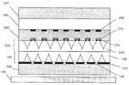
도 10A 및 도 10B는 반투과기(200)의 반투과형 픽셀(270) 및 광학소자층(250)을 갖는 시스템의 실시예들이다.10A and 10B are embodiments of a system having a
도 11A 및 도 11B는 반투과기(200)의 반투과형 픽셀(270), 광시준장치(100) 및 광학소자층(250)을 실시예들이다.11A and 11B illustrate embodiments of the
도 12는 두 개의 층을 갖는 광시준 또는 집속 구조물(400)의 일 실시예의 3차원 묘사도로서, 각 층은 렌즈상 채널인 광학소자들로 구성되는데, 렌즈상 채널의 수직면단면은 4면을 가지며(예를 들어, 사다리형 또는 곡면을 갖는 형상) 수평면단면은 렌즈상 채널과 동일한 길이를 갖는 장방형이다.12 is a three-dimensional depiction of one embodiment of a light collimation or focusing structure 400 having two layers, each layer consisting of optical elements that are lenticular channels, the vertical cross section of the lenticular channel being four sides. The horizontal cross-section is rectangular (eg, shaped like a ladder or curved surface) and has the same length as the lenticular channel.
이하는 본 명세서에서 이용하는 선택용어의 정의를 포함한다. 이 정의들은 용어의 범위 내에 속하고 실현 가능하게 사용할 수 있는 구성부품의 다양한 예 및/ 또는 형태들을 포함한다. 이 예들은 한정되는 것은 아니다. 이들 정의 내에는 영어의 단수형태 및 복수형태가 모두 있다.The following includes definitions of optional terms used in this specification. These definitions include various examples and / or forms of components that fall within the scope of the term and may be used in a practical manner. These examples are not limited. Within these definitions there are both singular and plural forms of English.
여기서 사용하는 "수평면 단면"이라는 것은 요소의 방향에 수직한 면을 따라서 취한 단면을 의미한다.As used herein, the term "horizontal plane cross section" means a cross section taken along a plane perpendicular to the direction of the element.
여기서 사용하는 "테이퍼형"이라는 것은 상기 수직면 단면 방향으로 직선 또는 곡선을 따라서 좁아지므로 다른 위치에서 취한 수평면 단면이 다른 면적을 갖게 되는 것을 의미한다. 다시 말해서, 테이퍼형 물체는 소면적의 단부와 대면적의 단부를 가질 것이다.The term " tapered " as used herein means that the horizontal cross-section taken at different positions has a different area because it narrows along a straight line or curve in the vertical plane cross-sectional direction. In other words, the tapered object will have an end of a small area and an end of a large area.
여기서 사용하는 "수직면 단면"이라는 것은 요소의 방향에 평행한 면을 따라서 취한 단면을 의미한다.As used herein, the term "vertical plane cross section" means a cross section taken along a plane parallel to the direction of the element.
본 출원은 (1) 반투과형 구조물 및 (2) 광시준 또는 광집속 구조물에 관한 것이다. 집속(funneling)은 기본적으로 깔때기의 작용이다. 깔때기는 통상적으로 액체나 미세입자 물질을 작은 개구로 용기 속에 안내하기 위한 장치로서 이용하는 원추형으로 형성된 파이프로 정의된다. 본 출원에서 깔때기는 일반적인 형상만을 의미하는데, 이 형상에는 작은 단부가 큰 단부가 있는데, 전체구조는 반드시 원추형은 아니다. 반투과형 응용에서의 광의 집속은 기본적으로 큰 단부에서 작은 단부로 이루어진다. 시준 용도에서의 광의 집속은 기본적으로 작은 단부에서 큰 단부로 이루어진다.The present application relates to (1) transflective structure and (2) light collimation or light focusing structure. Funneling is basically the function of the funnel. A funnel is typically defined as a conically formed pipe that serves as a device for guiding a liquid or microparticle material into a container with a small opening. In the present application, the funnel means only a general shape, which has a small end with a large end, and the overall structure is not necessarily conical. The focusing of light in transflective applications consists essentially of large to small ends. Focusing of light in collimation applications consists essentially of small to large ends.
광시준은 주어진 각도분포를 좁아지게 하는 방법에 의해 광원의 주어진 각도분포를 취하고 축상에 있는 피크강도를 증대시키는 것으로 정의된다.Light collimation is defined as taking a given angle distribution of a light source and increasing the intensity of the on-axis peak by a method of narrowing a given angle distribution.
광시준이나 집속 효과는 광학소자의 테이퍼형 단부의 위치와 형상에 따라서, 내부에 개구 또는 구멍을 갖는 반사층 및 매몰층과 함께 일련의 개별적인 테이퍼형 광학요소에 의해 형성된 광학층을 사용하여 성취할 수 있다. 광시준 또는 집속 기능을 수행하기 위해, 광학요소는 광원쪽으로 테이퍼를 형성하므로, 광학요소는 대면적의 단부와 소면적의 단부를 갖는다. 이렇게 소면적의 단부는 광입력 단부가 되고 대면적 단부는 광출력단부가 된다.The light collimation or focusing effect can be achieved by using an optical layer formed by a series of individual tapered optical elements together with a buried layer and a reflective layer having openings or holes therein, depending on the position and shape of the tapered end of the optical element. have. In order to perform the light collimation or focusing function, the optical element tapers toward the light source, so that the optical element has an end of a large area and an end of a small area. Thus, the end of the small area becomes the light input end and the large area end becomes the light output end.
도 1A는 광입력단부(12), 광출력단부(14) 및 엣지(16)를 갖는 광학요소(10)의 일 실시예를 예시한다. 본 실시예에서, 엣지(16)는 복합포물면(Compound Parbolic Concentrator; CPC) 같이 구속된다. 다시 말해서, 광학요소(1)의 수직면단면은 포물선 또는 대략 포물선이다. 본 실시예에서 광학요소(10)는 원형의 수평면단면을 갖는다. 다른 실시예(도시하지 않음)에서는 수평면단면이 사각형 또는 직사각형이다.1A illustrates one embodiment of an
도 1B는 동일한 광학요소(10)의 수직면단면의 묘사를 예시한다. 예시한 바와 같이, 광(L)은 여러 방향에서 광입력단부(12)에서 광학요소(10)로 들어간다. 광(L)이 광학요소(10)를 통해 이동함에 따라서, CPC 또는 포물선형 측벽(16)과 충돌한다. CPC 또는 포물선형 측벽은 광(L)을 반사시켜서 광(L)이 광출력단부(14)로부터 실질적으로 균일한 시이트로서 나오도록 광을 포커싱한다.1B illustrates a depiction of the vertical section of the same
도 2A는 광입력단부(21), 광출력단부(22) 및 정방형 수평면단면을 갖는 광학요소의 다른 실시예를 예시한다. 이하에 자세히 도시하는 바와 같이, 정방형 단면은 광학소자어레이에 광학소자가 고밀도로 팩킹되게 한다. 다른 실시예(도시하지 않음)에서는, 광학요소가 직사각형 또는 규칙적인 어떤 다각형의 수평단면도 가질 수 있다. 일반적으로 규칙적인 다각형 단면은 원형 단면보다 고밀도로 팩킹되게 한다.2A illustrates another embodiment of an optical element having an
계속하여 도 2A를 참조하면, CPC구조물(23)은 광학소자(20)의 광입력단부(21)에 위치하고 선형부(24)는 광출력단부(22)에 위치한다. 다른 실시예(도시하지 않음)에서는, 도 1에 도시한 것과 유사한 CPC단면이 도 2A에 도시한 CPC구조물(23) 및 선형부(24)의 복합물로 대체된다.With continued reference to FIG. 2A, the
도 2B는 광입력단부(21), 광출력단부(22) 및 정방형 단면을 갖는 광학소자(20)의 일 실시예를 예시한다. 본 실시예에서, 광학소자(20)는 광입력단부에서 곡선부(25)를 포함하는데, 상기 곡선부(25)는 CPC에 근사하도록 원의 원호에 의해 형성된다. 광학소자(20)는 광출력단부(22)에 위치하는 선형부(24)를 더 포함한다. 본 실시예에서, CPC구조물은 곡선부(25)의 경사와 선형부(24)의 경사를 곡선부(24) 및 선형부(25)의 교차점에서 일치시킴으로써 근사하게 된다.2B illustrates one embodiment of an
도 2C는 정방형 광입력단부(21)와 정방형 광출력단부(22)를 갖는 광학요소의 다른 실시예를 예시한다. 본 실시에에서, 제 1 선형부(24)는 광출력단부(22)에 위치하고 제 2 선형부(26)는 광입력단부(21)에 위치한다. CPC구조물(25)은 제 1 선형부(24)와 제 2 선형부(26)의 사이에 위치한다. 다른 실시예(도시하지 않음)에서는, CPC구조물(25)이 CPC구조물의 원형 근사구조물로 대체된다. 어떤 실시예서라도 제조를 가능하기 위해서는 최소의 드래프트 각도(θ)가 필요하다. 이 드래프트 각도는 광출력영역(22)과 선형부(24)의 면 사이에 형성되는 각도의 여각으로 정의 된다. 일 실시예에서, 드래프트 각도는 제 1 선형부(24)와 CPC구조물 사이와 CPC구조물과 제 2 선형부(26) 사이에 연속성 및 연속적의 경사가 있도록 선택된다.2C illustrates another embodiment of an optical element having a square
도 3은 정방형 광입력단부(32)와 정방형 광출력단부(34)를 갖는 광학소자(30)의 일 실시예의 수직면단면과 동등한 면의 측면도를 예시한다. 본 실시예에서는 선형부가 없다. 대신에, 광학소자(30)의 측면(36)이 CPC구조물의 원형 근사면이다.3 illustrates a side view of a plane equivalent to a vertical cross section of an embodiment of an
다른 실시예(도시하지 않음)에서, 광학소자는 제한 없이, 피라미드형, 원추형, 또는 그 외의 3차원 다각형이나 다면체를 포함한 어떤 적절한 테이퍼형 형상도 가질 수 있다. 또한, 광학소자의 개개의 면들은 광학소자의 내부로 들어오는 광을 제어하거나 집속하거나 시준할 수 있도록 평면형상, 오목형상, 볼록형상 또는 오목점형상이 될 수 있다.In other embodiments (not shown), the optical element may have any suitable tapered shape including, without limitation, pyramidal, conical, or other three-dimensional polygons or polyhedra. In addition, the individual surfaces of the optical element may be planar, concave, convex or concave point so as to control, focus or collimate the light coming into the optical element.
다른 실시예(도시하지 않음)에서, 광학소자는 교차 만입부, 비교차 만입부, 원추형, 원추형 단면, 3차원 포물선구조, 피라미드형, 다각형, 다면체형(예를 들어 4면체), 규칙적인 다면구조 또는 비규칙적인 다면구조를 갖는다. 광학소자의 반사율, 투과율 및 흡수율은 다른 값을 가질 수 있다. 이 구조물들의 측면들은 선형, 비선형 또는 이들의 조합일 수 있다.In other embodiments (not shown), the optical elements may be intersecting indentations, non-crossing indentations, conical, conical cross sections, three-dimensional parabolic structures, pyramids, polygons, polyhedrons (e.g. tetrahedrons), regular polyhedrons. It has a structure or irregular facet structure. The reflectance, transmittance and absorption of the optical element may have different values. Aspects of these structures can be linear, nonlinear, or a combination thereof.
CPC형상의 근사형상은 진정한 CPC형상보다 제조하기가 쉽고, 최고성능을 유지하거나 심지어는 향상시킨다. 원형의 원호는 성능을 향상시킬 수 있는 CPC의 근사형의 일 예이다. CPC구조물은 CPC의 각 면에서의 선형 영역의 조합이나 원의 원호로 근사될 수 있다. CPC구조물과 두 개의 선형 영역의 조합은 하나의 선형 영역 으로 근사될 수 있지만 성능은 감소한다. 일 실시예에서, 수평면단면은 직교하는 렌즈상 채널을 형성하여 이 구조물을 쉽게 제조할 수 있도록 정방형이나 장방형이 될 수 있다. 적어도 두 개의 비직교형 렌즈상 채널을 형성하면 시준구조물의 다른 단면을 만들 수 있다. 이 단면은 또한 어떤 규칙적 또는 비규칙적 다면체 또는 어떤 규칙적 도는 비규칙적 다각형도 될 수 있다.Approximate shapes of CPC shapes are easier to manufacture than true CPC shapes, maintaining or even improving top performance. Circular arcs are an example of approximations of CPCs that can improve performance. The CPC structure can be approximated by a combination of linear regions or circular arcs on each side of the CPC. The combination of the CPC structure and the two linear regions can be approximated as one linear region, but the performance is reduced. In one embodiment, the horizontal cross section may be square or rectangular to form orthogonal lenticular channels to facilitate fabrication of the structure. Forming at least two non-orthogonal lenticular channels can produce different cross sections of the collimation structure. This cross section may also be any regular or irregular polyhedron or any regular or irregular polygon.
장방형의 수평면단면(대응하는 장방형 입력단부를 가짐)은 대칭형상이 아닌 시준형 광출력부가 된다. 이 장방형 입력구조물의 전장을 따라서의 광출력의 각도분포는 그 폭을 따라서의 광의 각도분포보다 크다. 장방형 입력구조물의 길이를 증대시키면 광학요소의 출력영역에 대한 입력영역이 증가하여 광학요소의 출력에서 이용할 수 있는 총에너지가 커진다. 따라서, 출력광의 각도분포는 디스플레이 용도에 따라서 결정될 수 있다. 출력영역에 대한 입력영역은 출력광의 각도분포를 제어할 수 있도록 하는 장치의 설계변수이다. 이는 예를 들어 수평방향이 수직방향보다 넓은 시각(viewing angle)을 필요로 하는 액정디스플레이 텔레비전(LCD-TV)에 응용할 수 있다. 넓은 시각에 대한 필요조건을 만족시키기 위해서는, 입력구조물의 길이는 수평방향으로 이어지는 한편 폭은 수직방향으로 이어질 것이다.The rectangular horizontal section (with the corresponding rectangular input end) becomes a collimated light output rather than a symmetrical shape. The angular distribution of light output along the entire length of this rectangular input structure is larger than the angular distribution of light along its width. Increasing the length of the rectangular input structure increases the input area to the output area of the optical element, thereby increasing the total energy available at the output of the optical element. Therefore, the angular distribution of the output light can be determined according to the display use. The input area to the output area is a design variable of the device that allows to control the angle distribution of the output light. This can be applied to, for example, a liquid crystal display television (LCD-TV) in which the horizontal direction requires a wider viewing angle than the vertical direction. In order to meet the requirement for a wide field of view, the length of the input structure will run in the horizontal direction while the width will run in the vertical direction.
일 실시예에서, 드래프트 각도는 약 8°이상이 되므로 제 2 선형부가 전체장치를 형성하도록 연장된 것과 동일한 성능을 갖는 장치를 만들 수 있다. 다시 말해서, 이 성능은 제 1 선형부와 CPC가 제거되어 제 2 선형부의 연장부로 대체된 것처럼 될 수 있다. 이런 설계는 제조의 편리성을 고려하여 선택하겠지만, 성능은 낮아진다. 드래프트 각도가 작아지면 높은 성능을 갖지만 종횡비(aspect ratio)가 커지기 때문에 제조하기 어렵게 된다. 종횡비는 입력구멍 사이의 거리에 대한 광가이드의 깊이의 비로서 정의된다. CPC(또는 CPC에 맞는 원형) 장치는 동일 성능의 높은 종횡비의 선형장치보다는 장치를 제조하기 쉬운 낮은 종횡비의 설계를 가능하게 한다. 예를 들어, 3.5°(또는 8:1에 가까운 종횡비)의 드래프트 각도는 종횡비가 약 2.9:1인 CPC(또는 원형의 동등한 면)와 동일한 성능을 가질 것이다. 다른 실시예에서, CPC근사면은 1:1보다는 작고 약 7.5:1보다는 큰 종횡비의 범위를 갖는다.In one embodiment, the draft angle is greater than about 8 ° so that the device can be made with the same performance as the second linear portion is extended to form the entire device. In other words, this performance may be as if the first linear portion and the CPC were removed and replaced with an extension of the second linear portion. This design will be chosen considering the convenience of manufacturing, but the performance will be lower. The smaller the draft angle, the higher the performance, but the greater the aspect ratio, making it difficult to manufacture. Aspect ratio is defined as the ratio of the depth of the light guide to the distance between the input holes. CPC (or CPC-fitting) devices allow the design of low aspect ratios that are easier to manufacture devices than high aspect ratio linear devices of equal performance. For example, a draft angle of 3.5 ° (or aspect ratio close to 8: 1) will have the same performance as a CPC (or equivalent face of a circle) with an aspect ratio of about 2.9: 1. In other embodiments, the CPC approximation ranges from an aspect ratio less than 1: 1 and greater than about 7.5: 1.
도 4는 광학소자어레이(광학소자층이라고도 한다)의 일 실시예를 예시한다. 여기서 광학소자어레이는 10×10소자의 어레이(총 100개의 소자)다. 그러나 다른 실시예에서는 광학소자어레이가 어떤 원하는 사이즈도 될 수 있으며, 어떤 원하는 개수 또는 배치의 광학소자도 포함할 수 있다.4 illustrates one embodiment of an optical element array (also called an optical element layer). The optical element array is an array of 10 x 10 elements (100 elements in total). However, in other embodiments, the optical element array can be any desired size and can include any desired number or arrangement of optical elements.
다른 실시예(도시하지 않음)에 있어서, 광학소자는 다양한 패턴으로 배열된다. 예를 들어, 광학소자들은 막의 영역 전역에 걸쳐서 평행하게 이격되어 반복될 수 있다. 광학소자들은 패턴이 반복되기 전에 다양한 형상, 높이, 각도 또는 간격으로 배열될 수 있다. 다른 방법으로서, 광학소자들은 패턴을 인식할 수 없을 정도로 무질서하게 배열될 수 있다. 원치 않는 수차의 효과(무아레(Moire) 효과 등)를 제거하거나 줄이기 위해서는 구조물의 우연한 변화 또는 파괴적 구조물이라고 부를 수 있는 것을 사용할 수 있다.In another embodiment (not shown), the optical elements are arranged in various patterns. For example, the optical elements can be repeated spaced apart in parallel across the region of the film. The optical elements may be arranged in various shapes, heights, angles or intervals before the pattern is repeated. Alternatively, the optical elements can be arranged in an orderly manner that cannot recognize the pattern. To eliminate or reduce the effects of unwanted aberrations (such as the Moire effect), one can use what can be called accidental changes or destructive structures.
일 실시예에서, 공기의 굴절율을 초과하는 굴절율을 갖는 고투과성 폴리머로 광학층이 형성된다. 일 실시예에서, 광학소자의 영역을 포함하는 광을 형성하는데 사용하는 폴리머의 굴절율은 적어도 약 1.1이거나 심지어 적어도 약 1.2이다. 다른 실시예에서, 광학소자의 광포함영역을 형성하는데 사용되는 폴리머의 굴절율은 약 1.3 내지 약 1.8의 범위에 있다. 이 영역은 어떤 상용성(compatible) 재료로도, 예를 들어 광포함영역보다 낮은 굴절율을 갖는 공기나 폴리머로도 둘러싸여져서 광포함영역의 내부경계(장치의 내측경계)에서 전반사(TIR)되게 한다. 광학소자의 광포함영역의 폴리머의 굴절율이 낮아질수록 입력단부 및 출력단부의 외측공기경계에서의 프레넬(Fresnel) 손실이 작아진다. 낮은 굴절율로 이득을 향상시키는 이런 방법은 내측경계에서 전반사가 일어나게 할 수 있을 정도로 충분히 낮은 굴절율의 상용성 재료를 찾기 위한 필요조건에 의해서만 한정된다.In one embodiment, the optical layer is formed of a highly transparent polymer having a refractive index above that of air. In one embodiment, the refractive index of the polymer used to form the light including the area of the optical element is at least about 1.1 or even at least about 1.2. In another embodiment, the refractive index of the polymer used to form the light containing region of the optical device is in the range of about 1.3 to about 1.8. This area is surrounded by any compatible material, for example air or polymer, which has a lower refractive index than the light containing area, causing total internal reflection (TIR) at the inner boundary of the light containing area (inner boundary of the device). The lower the refractive index of the polymer in the light containing region of the optical element, the smaller the Fresnel loss in the outer air boundary of the input and output ends. This method of improving gain with low refractive indices is limited only by the requirement to find compatible materials with refractive indices low enough to cause total internal reflection at the inner boundary.
도 5A, 도 5B 및 도 5C는 각각 광시준 또는 집속 구조물의 분해도, 조립도 및 측면도(수직면단면과 동등한 면)를 보여준다. 또한 도 5A, 도 5B 및 도 5에는 방출 및 반사면으로서 동시에 작용하는 표면(12)을 갖는 백라이트(110)(LCD 티브이에서 사용되는 것 등)가 도시되어있다. 최첨단 기술에 익숙한 누구라도 이것은 LCD 백라이트의 표준특징이라는 것을 알 수 있을 것이다. 이 반사특징은 실행에 필요한 특성인 광재생을 가능하게 한다. 시준 또는 집속 구조물(100)은 반사층(14)이 상면에 형성된 매몰층(130)과 광학소자층(150)응 포함한다.5A, 5B and 5C show an exploded view, an assembly view and a side view (surface equivalent to a vertical section) of a light collimation or focusing structure, respectively. 5A, 5B and 5 also show a backlight 110 (such as used in LCD TVs) having a
일 실시예에서, 매몰층(130)은 폴리머재료로 구성된다. 프레넬 손실을 최소로 하기 위해서는 장치의 광포함영역과 동일한 굴절율의 광학적으로 투명한 재료를 필요로 한다. 다른 실시예에서는, 유리나 공기를 포함한 어떤 굴절율의 어떤 광학적으로 투명한 재료도 사용할 수 있다.In one embodiment, the buried
반사층(140)은 광학소자층(15)의 광학소자의 광입력측면(170)과 일치하는 구멍(또는 개구)(160)을 포함한다. 일 실시예에서, 반사층(140)은 수 미크론의 고반사 재료 박막을 고투과성 폴리머기재(매몰층(130)) 상에 스퍼터링 또는 화학증착(CVD)하고 광입력측면(170)의 위치에서 반사재료를 선택적으로 제거함으로써 형성된다. 반사층(14)의 구멍(160)도 광입력측면(170)의 재료를 연장하고 그 반사층(140)을 관통시킴으로써 형성된다. 일 실시예에서, 입력구멍은 반사층의 상면과 동일면상에 있다. 일 실시예에서, 반사층(140)은 니켈, 금, 알루미늄, 은 또는 그 외의 적합한 금속 등의 금속으로 구성된다. 그러나, 다른 실시예(도시하지 않음)에서는 반사층이 어떤 반사물질로도 구성될 수 있다.The
매몰층(130)을 구성하는데 사용되는 고투과성 폴리머기재는 광학소자층(150)의 광학소자에서 사용되는 것과 동일한 폴리머일 수 있다. 동일한 폴리머를 사용하게 되면 시준 또는 집속 구조물의 나머지 부분과 광학적으로 이음부 없는 계면이 되며 프레넬 손실을 최소화한다. 반사층(140)이 경면 또는 산만산란층으로서 작용하는 경우, 반사층(140)은 가능한 높은 반사율을 가지며, 일 실시예에서 정반사율 또는 난반사율이 95%를 초과한다. 장치의 광포함영역으로의 입력을 차단하는 반사성 재료인 반사성재료의 과잉분은 예를 들어 마스킹 및 에칭에 의해 제거하여 반사재료가 없는 영역들이 구멍(160)을 형성할 수 있다. 전술한 바와 같이, 구멍(160)에 형성된 반사층(140)은 적어도 하나의 반사층(140)이 백라이트(110)와 대향한다면 매몰층(130)의 어느 측면에도 위치할 수 있다.The highly permeable polymer substrate used to construct the buried
여기서, 반사층(140)은 광이 광원으로부터 반사에 의해 재순환되게 하는 얇 은 정반사 또는 난반사층으로서 작용한다. 다른 실시예에서는 반사층(140)이 정반사층이 아니라 난반사층이다. 그러나, 바람직한 실시예는 광선추적계산(ray-tracing calcualtion)에 따르면 정반사층에 비하여 난반사층의 성능이 저하한다는 것을 보여주기 때문에 정반사층(140)이 적합하다. 또 다른 실시예에서, 반사층(140)의 표면은 광을 입력구멍 속으로 보다 효율적으로 안내하도록, 즉 반사수가 최소가 되고 에너지손실이 최소가 되도록 (예를 들어, 딤플 등의 계통적이거나 무질서한 함몰부 또는 융기부를 갖도록) 조직이 처리된다. LCD백라이트 반사체의 반사면도 반사수를 최소로 하면서 광을 입력구멍 속으로 안내하기 위한 동일한 목적으로 장치의 반사층과 일치하도록 광학적으로 조정할 수 있다.Here, the
도 5A, 도 5B 및 도 5C를 계속 참조하면, 반사층(140)은 백라이트(110)의 반대측의 매몰층(130)의 측면에 배치된다. 다른 실시예(도시하지 않음)에 있어서, 반사층(140)은 백라이트(110)와 대향하는 매몰층(130)의 측면에 배치된다. 어떤 실시예에서도 반사층(140)은 광을 재순환하도록 백라이트(110)쪽으로 반사시킨다.5A, 5B, and 5C, the
본 실시예에서, 시준 또는 집속 구조물(100)은 광입력측면(170) 및 광출력측면(180)을 갖는 다수의 3차원 광학소자로 형성된 광학층(150)을 포함한다. 도 5A, 도 5B 및 도 5C에 예시한 실시예에서, 광학소자들은 서로 결합되어 그들의 광출력측면(180)에서 시이트를 형성하므로 연속적인 시준막을 만들게 된다. 도 6에 도시한 다른 실시예에서, 광학소자의 광포함영역은 별개로 되어 서로 분리되어 있지만 공통 폴리머 시이트(185)에서 결합되어있다.In the present embodiment, the collimation or focusing
도 5A, 도 5B 및 도 5C에 예시한 실시예에서, 광학소자층(150)의 광입력측 면(170)은 반사층(140)과 접촉하고 있으므로 광학층(150)의 광학소자들은 반사층(140)에 형성된 구멍(150)들과 대응하게 된다. 도 6에 도시한 다른 실시예에서, 광학소자층(150)의 광학소자들은 반사층(140)을 매립하도록 연장된다. 다시 말해서, 광입력측면(170)은 반사층(140)의 구멍(160) 속으로 연장되어 매몰층(130)과 접촉하게 된다. 본 실시예에서는 매몰층(130)과 광학소자층(150) 사이에 틈새가 없다. 이것은 매몰층(130)과 광학소자층(150)을 단일연속층으로서 제조하고 나중에 반사층(140)을 광학소자층(150) 위에 연결(예를 들어, 적층)시킴으로써 얻을 수 있다.5A, 5B, and 5C, the optical
또 다른 실시예(도시하지 않음)에 있어서, 반사층(140)은 백라이트와 대향하는 매몰층(130)의 측면에 형성되고, 광학소자의 광입력측면(170)은 매몰층(130)과 접촉되어있다.In another embodiment (not shown), the
매몰층(130)에 대한 반사층(140)의 위치결정에 관계없이, 반사층(140)은 백라이트(110)와 대향한다. 백라이트(110)로부터 방출된 광은 시준되기 위해서 궁극적으로는 반사층(140)의 구멍(160)을 통과하고 그 후 광학층(150)의 광학소자를 통과하여야 한다. 구멍(160)을 통과하지 않는 광은 백라이트(110)로 다시 반사되고, 백라이트는 그 광을 구멍쪽으로 다시 반사시킨다. 그 후 이 광은 구멍(160)을 통과하거나 흡수에 의해 광학계에서 없어질 때까지 반복적으로 반사된다. 시준된 광의 출구각도분포는 여러 가지 LCD디스플레이 타입에서 볼 수 있는 픽셀수용각도의 범위와 일치하도록 설계될 수 있다. 이렇게 하면 LCD에 의해 처리할 수 있는 픽셀에 입사하는 광의 양을 최대로 할 수가 있으므로, 관찰자가 감지하는 휘도를 최대 화할 수 있다.Regardless of the positioning of the
한 타입의 반투과형 LCD에 있어서는, 구조물(100)과 픽셀의 반사부의 후면에서 반사되는 광 사이에서 추가로 광의 재순환이 일어날 수 있다. 이런 타입의 반투과형 LCD는 투과형 구멍 및 반사영역을 모두 가지는 픽셀로 구성된다. 다른 타입의 반투과형 LCD는 픽셀이 투과성이고 반사영역이 픽셀의 외부의 광학소자에 위치한다. 이런 반투과형 LCD와 투과형 LCD 사이의 큰 차이는 픽셀의 외부의 광학소자에 위치하는 반사영역이다. 반투과형 CLD는 여기서 개시하는 시준장치를 포함할 수 있다.In one type of transflective LCD, further recycling of light may occur between the
도 7A 및 도 7B는 광시준 및 집속 구조물(100)의 다른 실시예를 예시하는데, 여기서 광소자층의 광소자들 사이의 공기공간에 충전재(190)가 채워져 있다. 본 실시예에서, 충전재(190)는 광소자용으로 사용되는 고투과성 폴리머보다 충분히 낮은 굴절율을 갖는 폴리머재료로 구성된다. 폴리머의 굴절율 차이는 TIR(전반사)를 유지하도록 선택할 수 있다. TIR을 유지하는데 필요한 영역의 굴절율의 차이는 광포함영역의 굴절율이 증가함에 따라서 감소한다. 충전재(190)의 투과율은 그 충전재를 어떤 광도 통과하지 않기 때문에 높을 필요는 없다. 실제로, 충전재(190)의 투과율은 제로가 될 수 있기 때문에, 충전재(190)로서 금속을 사용할 수 있다. 금속의 반사율은 광포함영역의 경계로부터 광이 반사할 때 (금속에 의한 흡수나 산란에 의해) 에너지손실을 최소로 할 수 있을 정도로 충분히 높아야 한다. 광포함영역의 입력구멍 사이의 표면은 공기 대신에 폴리머 충전재(190)를 사용하여 반사재료의 표면을 형성하여 광원으로부터의 광이 재순환할 수 있도록 하는 반사재료로 덮어져야 한다. 제조방법은 마스크를 통한 침착 또는 에칭에 의해 반사표면(140)을 형성할 수 있다. 폴리머 매몰층(110)은 또한 프레넬 손실을 제한하는데도 사용할 수 있다. 본 실시예는 도 7A 및 도 7B에 도시하는데, 여기서 사용하는 동일한 참조부호는 도 5A, 도 5B 및 도 5C를 참조하여 설명한 광시준 및 집속 구조물(100)의 동일한 부분들을 지시한다. 이와 같이 도 7A 및 도 7B에 개시한 전체구조물(100)의 설명은 간결성을 위해 생략한다.7A and 7B illustrate another embodiment of the light collimation and focusing
일 실시예에서, 광학소자층(150)의 굴절율은 충전재(190)의 굴절율보다 크다. 광학소자층(150)의 굴절율은 광포함영역으로부터의 광누출 없이 광포함영역의 내측경계(장치의 내측경계)에서 전반사되도록 충전재(190)의 굴절율보다 충분히 크다. 이 차이는 약 0.15가 되는 것으로 계산되는데, 원하는 차이 값이 높으면 광학소자의 굴절율이 낮아지고 원하는 차이값이 낮으면 굴절율이 높아진다. 전술한 누출 없이 전반사를 만들기 위한 최소 차이가 만족되는 한, 공기공간을 점유/충전하는 폴리머와 광학소자층(150)을 형성하는데 사용되는 폴리머 사이의 굴절율의 차이에는 상한이 없음을 알아야 한다.In one embodiment, the refractive index of the
도 8은 본 출원의 다른 실시예에 따른 반투과형 구조물(200)을 예시한다. 이 반투과형 구조물(200)은 제 1 방향에서(즉 태양이나 실내조명 등의 주변광원(A)에서) 도착하는 광을 반사하고 반대방향에서(즉, 백라이트(110)에서) 도달하는 광을 반사시킨다. 본 실시예에서, 반투과형 구조물(200)은 매몰층(230), 광학층(250) 및 반사층(240)으로 구성될 수 있는데, 반사층(240)은 출력구멍(260)만을 제외하고 광학소자(250)의 표면을 덮어서 반사면적을 최대로 하려는 것이다. 반투 과형 구조물(200)의 구성요소들은 광시준 또는 집속 구조물(100)에서 사용된 것과 실질적으로 동일하지만, 역으로 되어있다.8 illustrates a
도 8에 예시한 실시에에서, 반투과형 구조물(200)은 백라이트(110)와 주변광원(A)의 사이에 위치한다. 반사층(240)은 구멍(또는 개구)(260)이 형성되어 있으므로, 백라이트(110)로부터의 광을 투과하는 한편 주변광원(A)으로부터의 광을 반사시킬 수 있게 되어있다. 도 8에서, 반사층(240)은 광학층(250)과 대향하는 매몰층(230)의 측면에 형성된다. 다른 방법으로서, 반사층(240)은 주변광원(A)과 대향하는 매몰층(230)의 측면에 형성되거나 또는 매몰층(230)의 양측면에 형성될 수 있다. 그 외의 매몰층(230) 및 반사층(240)의 구조 및 특성들은 광시준 또는 집속 구조물(100)과 관련하여 전술한 매몰층(130) 및 반사층(140)과 실질적으로 유사하다. 이와 같이 도 8에 개시된 매몰층(230) 및 반사층(240)의 특성 및 전체구조의 설명은 간결성을 위해 생략한다.In the embodiment illustrated in FIG. 8, the
광학층(250)은 도 1A, 도 1B, 도 2A, 도 2B, 도 2C 및 도 3에 도시한 것 같은 3차원 테이퍼형 광학소자로 형성될 수 있다. 본 실시에에서, 광학소자의 소면적단부는 주변광원(A)과 대향하며, 따라서 백라이트(110)로부터 전달된 광에 대한 광출력단부로서 작용한다. 광학층(250)의 광학소자의 광출력단부는 반사층(240)에 형성된 구멍(260)에 대응한다. 본 실시예에서, 광출력단부는 반사층(240)과 접촉하도록 연장된다. 다른 실시예에서, 광출력단부는 도 6에 도시한 바와 같이 반사층(240)을 매립하도록 연장된다. 또 다른 실시예에서, 반사층(240)은 광학층(26)의 반대측의 매몰층(230)의 측면에 형성되고 광학소자의 광출력단부는 매몰층(230) 과 접촉한다.The
그 외의 광학층(250)의 구조 및 특성들은 도 5 - 도 7과 관련하여 전술한 광학층(150)과 실질적으로 유사하다. 이와 같이 도 8에 개시한 광학층(260)의 전체구조 및 특성의 설명은 간결성을 위해 생략한다.The structure and characteristics of the other
도 9는 반투과형 구조물(200) 및 광시준 또는 집속 구조물(100)을 모두 갖는 반투과기(transflector)(300)를 예시한다. 반투과기(300)는 제 1 방향에서(즉, 태양이나 실내조명 등의 주변광원(A)에서) 도달하는 광은 반사시키고 반대방향에서(즉, 백라이트(110))에서 도달하는 광은 투과시킨다. 도시한 실시예에서, 백라이트(110)와 반투과형 구조물(200) 사이에는 광시준 또는 집속 구조물(100)이 위치하므로, 백라이트(110)에서 방출된 광은 먼저 광시준 또는 집속 구조물(100)에 의해 시준되거나 집속된 후 반투과형 구조물(200)을 통해 투과된다. 동시에, 주변광은 반사층(240)으로 반사된다.9 illustrates a
다른 실시예(도시하지 않음)에 있어서, 반투과형 구조물(200)은 백라이트(110)와 광시준 또는 집속 구조물(100) 사이에 위치하므로, 백라이트(110)에서 방출된 광은 먼저 반투과형 구조물(200)을 통해 투과된 후 광시준 또는 집속 구조물(100)에 의해 시준 또는 집속되는 한편 주변광은 반사층(140)으로 반사된다. 광시준 또는 집속 구조물(100) 및 반투과형 구조물(200)은 도 5 - 도 7과 관련하여 설명한 것과 실질적으로 동일하다. 이와 같이, 도 9에 개시한 전체 광시준 또는 집속 구조물(100) 및 반투과형 구조물(200)의 설명은 간결성을 위해 생략한다.In another embodiment (not shown), since the
도 10A는 반투과기(200)의 광학층(250) 및 반투과형 픽셀(270)을 이용하는 디스플레이를 예시한다. 도 10A에 예시한 실시예에서, 반투과형 픽셀(270)는 반사층(275)을 갖는다. 반투과형 픽셀(270)는 광학층(250)의 광포함영역의 광출력단부와 일치하도록 정렬되어있다. 픽셀(270)는 반사층(275)을 포함하기 때문에, 반투과기(200)는 반사층이 필요 없다. 본 실시예에서, 반투과형 픽셀(270)는 액정서스펜션(280) 속에 위치한다. 액정서스펜션(280) 속에는 칼라필터(285)도 위치한다. 칼라필터(285)는 반투과형 픽셀(270)과 일치하도록 정렬되며, 적색, 녹색 및 청색 칼라필터를 포함한다.10A illustrates a display using an
도 10A를 계속 참조하면, 백라이트(110)는 후면편광기(280)의 근처에 위치한다. 반투과기(200)의 광학층(250)은 후면편광기(290)와 액정서스펜션(280) 사이에 위치한다. 이 액정서스펜션(280)은 또한 전면유리(295)에 근접 위치한다. 전면유리는 또한 전면편광기(297)에 근접 위치한다. 픽셀(270)은 반사층(275)을 포함하기 때문에 반투과기(200)는 반사층이 필요 없다. 다른 실시예(도시하지 않음)에 있어서, 반투과기(200)와 액정서스펜션(280) 사이에는 후면유리가 배치된다. 또 다른 실시예(도시하지 않음)에 있어서, 반투과기(200)는 전면편광기(297)의 뒤에 위치한다.With continued reference to FIG. 10A, the
도 10B는 반투과기(200)의 광학층(250) 및 반투과형 픽셀(270)을 이용하는 디스플레이의 또 다른 실시예를 예시한다. 본 실시예에서, 칼라필터(285)는 액정서스펜션(280) 속에 위치하지 않는다. 대신에 후면편광기(290)와 후면유리(299) 사이에 칼라필터가 배치된다. 반투과기(200)의 광학층(250)은 백라이트(110)에 인접하게 위치하므로, 백라이트(110)와 후면편광기(290) 사이에 배치된다. 후면유 리(299)는 칼라필터(285)와 액정서스펜션(280) 사이에 배치된다. 도 10A에서처럼 전면편광기(297)와 액정서스펜션(280) 사이에는 전면유리(295)가 배치된다.10B illustrates another embodiment of a display utilizing the
도 11A는 반투과기(200)의 반투과형 픽셀(270), 시준장치(100) 및 광학층(250)을 이용하는 디스플레이를 예시한다. 도 11A에 예시한 실시예에서, 반투과형 픽셀(270)은 반사층(275)을 갖는다. 반투과형 픽셀(270)은 광학층(250)의 광포함영역의 광출력단부와 일치하도록 정렬된다. 역시 픽셀(270)은 반사층(275)을 포함하기 때문에 반투과기(200)는 반사층이 필요 없다. 시준장치(100)는 광학소자층(150)과 구정(160)을 갖는 반사층(140)을 포함한다. 본 실시예에서, 반투과형 픽셀(270)은 역시 액정서스펜션(280) 속에 위치한다. 칼라필터(285)는 반투과형 픽셀(270)과 일치하도로 정렬되며, 적색, 녹색 및 청색 칼라필터를 포함한다.11A illustrates a display using
계속해서 도 11A를 참조하면, 백라이트(110)는 후면편광기(290)에 근접하여 위치한다. 시준장치(100)는 후면유리(290)에 근접하므로, 후면유리는 백라이트(110)과 시준장치(100)의 사이에 배치된다. 반투과기(200)의 광학층(250)은 시준장치(100)와 액정서스펜션(280)의 사이에 위치한다. 액정서스펜션(280)은 역시 전면유리(295)에 근접 위치한다. 전면유리 또한 전면편광기(297)에 근접 위치한다. 다른 실시예(도시하지 않음)에 있어서, 반투과기(200)와 액정서스펜션(200)의 사이에는 후면유리가 배치된다. 다른 실시예(도시하지 않음)에서는 반투과기(200)와 시준장치(100)가 분리되어 있고 시준장치(100)가 전면편광기(297)의 뒤에 위치한다. 또 다른 실시예(도시하지 않음)에 있어서, 반투과기(200) 및 시준장치(100)는 모두 전면편광기(297)의 뒤에 위치한다.With continued reference to FIG. 11A, the
도 11B는 반투과기(200)의 광학층(250) 및 반투과형 픽셀(270)을 이용하는 디스플레이의 또 다른 실시예를 예시한다. 본 실시예에서, 칼라필터(285)는 액정서스펜션(280) 속에 위치하지 않는다. 대신에 칼라필터는 후면편광기(290)와 후면유리(299)의 사이에 배치된다. 시준장치(100)는 백라이트(110)에 근접하여 위치하므로, 반투과기(200)의 광학층(250)과 백라이트(110)의 사이에 배치된다. 후면편광기(290)는 반투과기(200)의 광학층(250)과 칼라필터(285)의 사이에 배치된다. 후면유리(299)는 칼라필터(285)와 액정서스펜션(280)의 사이에 배치된다. 도 11A에서처럼, 전면편광기(297)와 액정서스펜션(280)의 사이에는 전면유리(295)가 배치된다. 또 다른 실시예(도시하지 않음)에 있어서, 반투과기(200)와 시준장치(100)는 분리되어있으며, 반투과기(200)는 전면편광기(297)의 전방이면서 칼라필터(285)의 뒤에 배치된다.11B illustrates another embodiment of a display utilizing the
시준 또는 반투과장치 또는 이들의 조합은 LCD의 백패널의 일부로서 사용할 수 있다. 반투과형 장치를 백패널에 위치시키면 반사형(주변) 구성요소로부터 발생하는 변색(color shift) 및 시차효과(parallax effect)를 경감시킬 것이다. 이 것은 특히 플렉시블(소위 플라스틱) 디스플레이에 적용할 수 있다.Collimation or transflective devices or combinations thereof may be used as part of the back panel of the LCD. Positioning the transflective device in the back panel will mitigate color shift and parallax effects from reflective (peripheral) components. This is particularly applicable to flexible (so-called plastic) displays.
도 12는 광집속 또는 시준 소자(440)를 구비하는 제 1 및 제 2 광학소자층(410, 420)을 갖는 광시준 또는 집속 장치(400)의 일 실시예를 예시한다. 본 실시예에서, 각 광학소자(410, 420)는 렌즈상 채널인 광학소자로 형성되는데, 이 렌즈상 채널의 수직면단면은 4면(예를 들어, 사다리형 또는 굽은 측면을 갖는 형상을 포함)을 가지며 이 렌즈상 채널의 수평면단면은 렌즈상 채널과 동일한 길이를 갖는 장방형이다. 이전의 도면에서 개시한 바와 같이, 양 층에서 광학소자는 백라이트(도시하지 않음) 쪽으로 테이퍼가 형성되어있다.FIG. 12 illustrates one embodiment of a light collimation or focusing device 400 having first and second optical element layers 410, 420 having a light focusing or collimating
본 실시예에서, 광학소자층(410, 420)은 렌즈상 채널들이 서로 직교하도록 배치된다. 다시 말해서, 제 1 광학소자층(410)의 광학소자들은 제 2 광학소자층(420)의 광학소자의 수평면 장방형 베이스에 직교한다. 다른 실시예(도시하지 않음)에 있어서는, 제 1 광학소자층(410)의 렌즈상 채널이 제 2 광학소자층(420)의 렌즈상 채널에 대하여 예각 또는 둔각으로 놓인다. 일 실시예에서, 제 2 광학소자층(420)(백라이트에서 제일 먼 층)은 금속층(430)을 포함한다. 다른 실시예(도시하지 않음)에 있어서, 상층은 금속층을 포함하지 않는다. 추가의 다른 실시예(도시하지 않음)에서, 구조물(400)은 장방형 단면을 갖는 단일층의 광학소자를 포함한다.In the present embodiment, the optical element layers 410 and 420 are arranged so that the lenticular channels are orthogonal to each other. In other words, the optical elements of the first
구조물(100, 200, 300 또는 400)은 예를 들어 액정디스플레이(LCD) 등의 비발광 디스플레이 시스템, 또는 이미지를 형성하기 위한 목적으로 광이 안내되는 장치와 함께 사용할 수 있다. 통상의 이런 타입의 비발광 디스플레이 시스템은 백라이트, 편광기, 액정서스펜션 및 다른 편광기로 구성된 스택을 포함한다. 때때로 각 편광기와 액정서스펜션 사이에는 유리플레이트가 적층될 수 있다. 구조물(100, 200, 300 또는 400)은 백라이트와 편광기 사이에 위치할 수 있다. 동작에 있어서, 주변광이 다양한 층의 편광기, 유리플레이트(칼라필터, 공통전극, TFT매트릭스 또는 그 외의 부품) 및 액정서스펜션을 통과하여 액정의 배면유리플레이트의 내측에 위치하는 반사구조물에 의해 방향을 바꾸는 한편 동시에 백라이트 조립체에서 발생 한 인공광이 구조물(100, 200, 300 또는 400)을 통과할 것이다. 구조물(100, 200, 300 또는 400)은 LCD의 부분조립체의 일부로서 포함될 수 있거나 시준 또는 반사형 편광막 등의 그 외의 재순환막과 함께 사용될 수 있다.The
구조물(100, 200, 300 또는 400)은 백라이트 조립체와 액정모듈 사이에 삽입될 수 있는데, 여기서 구조물(100, 200, 300 또는 400)의 반사표면이나 반사표면들은 백라이트 조립체와 대향하고 투과표면은 액정모듈과 대향한다.The
LCD로부터 나오는 광의 통상적인 분포는 램버트(lambertian) 분포이다. 이런 분포는 시준성이 아니라고 생각된다. 구조물(100, 200, 300 또는 400)은 백라이트의 램버트 분포를 지정된 분포각도로 시준한다. 지정된 각도분포는 광포함 폴리머영역의 굴절율, 광포함영역의 길이 및 형상 및 입력 및 출력구멍의 사이즈에 따라서 다르다. 구조물(100, 200, 300 또는 400)의 반사표면은 백라이트 조립체와 대향하며, 백라이트 조립체에서 나와서 반사표면의 개구를 통과하는 광은 결국 액정모듈에 의해 처리된다.A typical distribution of light exiting the LCD is a lambbertian distribution. This distribution is not considered collimated. The
LCD의 내부에는 보통 공간이 있기 때문에, 구조물(100, 200, 300 또는 400)의 전체두께가 최소화되어야 한다. 일 실시예에서, 장치의 전체두께는 약 1000미크론미만, 또는 약 500미크론미만 또는 약 200미크론미만이 될 수 있다. 다른 실시예에서, 구조물(100, 200, 300 또는 400)은 어떤 정해진 두께에 한정되지 않는다. 오히려 구조물(100, 200, 300 또는 400)의 두께는 그 용도에 의해 결정되며 반드시 1000미크론에 한정되는 것은 아니다. 마찬가지로, 주기성의 선택은 LCD픽셀의 주기성에 의해 영향을 받는다. 장치에 대한 주기성들이 LCD에 대한 주기성보 다 작다면, 장치에서의 제조결함이 발견되기 어려워 결국 불합격된다. 장치에 대한 통상의 주기성은 1미크론미만에서 수백 미크론의 범위가 될 수 있다. 통상의 입력구멍 폭도 1미크론미만에서 수백 미크론의 범위이다. 잠재적인 회절효과를 다루기 위해 1미크론미만의 설계를 사용할 때는 특별한 주의를 기울여야 한다. 이런 가능한 설계범위에 기초하여 장치를 제조할 때는 나노복제 및 마이크로복제 방법을 둘 다 사용하기 쉽다. 구조물의 특징을 적절히 평가할 때에 성능이 유지될 것이다.Since there is usually space inside the LCD, the overall thickness of the
다른 실시예에서, 구조물(100, 200, 300 또는 400)은 (1) 액정모듈의 후면유리의 배면에서 그리고 편광기의 전방에서, (2) 액정모듈의 후면유리의 배면에서 그리고 편광기의 뒤에서, (3) 픽셀 레벨에서 액정모듈의 후면유리의 내부에서 3가지 구조로 액정모듈 자체 내에 위치할 수 있다. 2개의 편광기 액정디스플레이 시스템의 경우는, 광을 처리하기 위한 제 2 구조만이 가능하다. 단일 편광기 액정디스플레이 시스템의 경우는 3가지 구조 모두가 가능하다. 플라스틱 LCD에서 구조물(100, 200, 300 또는 400)은 백패널의 일부로서 이용될 수 있으며 반드시 1000미크론에 한정될 필요는 없다. 마찬가지로 주기성의 선택은 LCD픽셀의 주기성에 의해 영향을 받는다. 장치의 주기성이 LCD의 주기성보다 작다면, 장치의 제조결함을 보기가 어려워져 불합격이 된다. 장치의 전형적인 주기성은 1미크론미만에서 수백미크론의 범위가 될 수 있다. 전형적인 입력구멍의 폭도 1미크론미만에서 수백미크론의 범위이다. 잠재적인 회절효과를 다룰 때에는 특별히 주의를 기울여야 한다. 이런 가능한 설계의 범위에 기초하여, 장치의 제조에 나노복제 및 마이크로복 제 방법을 둘 다 사용할 수 있다. 구조적 특징을 적절히 평가한다면 성능이 유지될 것이다.In another embodiment, the
LCD는 전술한 실시예중의 어느 실시예에서도 LCD는 로울을 맞대어(roll-to-roll) 제조하거나 또는 적층식(layer-by-layer)으로 조립할 수 있으며, 광시준 또는 집속 구조물(100, 200, 300 또는 400)은 스택의 일체부가 될 수 있다. LCD스택의 층들은 적층식으로 제조 또는 조립되며, 구조물(100, 200, 300 또는 400)은 유리, 픽셀, 콜리메이터 또는 편광기의 일부로서 이용할 수 있다. 액정모듈 기판상에는 기능부품을 적층할 수 있으므로, 구조물(100, 200, 300 또는 400)을 전체 액정모듈제조공정의 일부로서 구성할 수 있다.The LCD may be manufactured roll-to-roll or assembled in a layer-by-layer, in any of the embodiments described above, and may be provided with a light collimation or focusing
일 실시예에서, 비발광 디스플레이 시스템은 광의 대부분이 장치에 수직하게 나오도록 광을 시준한다. 이 비발광 디스플레이 시스템은 또한 편광자를 포함할 수 있다. 어떤 실시예에서도 장치의 반사성 또는 반투과성 측면에는 시준 또는 편광 재료를 부착할 수 있다. 구조물(100, 200, 300 또는 400)의 고투과성 표면은 액정모듈과 대향하며 고반사성 표면은 백라이트 조립체와 대향할 수 있다. 구조물(100, 200, 300 또는 400)의 전체 투과성 표면에는 시준 또는 편광 재료가 부착될 수 있다. 이 시준 또는 편광 재료는 일체적 설계요소가 되며 제조된 제품의 일부가 될 수 있다. 다른 방식으로서, 이 재료는 구조물(100, 200, 300 또는 400)의 어느 표면에도 나중에 부착 또는 고정될 수 있다. 일 실시예에서, 광이 구조물(100, 200, 300 또는 400)에서 나오는 경우 표면의 전역을 시준막이 덮을 수 있다. 시준막은 디스플레이의 전역 또는 적어도 일부를 덮을 수 있다.In one embodiment, the non-luminescing display system collimates the light such that most of the light exits perpendicular to the device. This non-luminescent display system can also include a polarizer. In any embodiment, a collimating or polarizing material may be attached to the reflective or semi-permeable side of the device. The highly transparent surface of the
광을 시준하는 다른 방법은 액정디스플레이 시스템 내의 소형렌즈(lens-let)를 포함하는 것이다. 그 위치는 구조물(100, 200, 300 또는 400) 내에 일체로 되거나 분리될 수 있으며, 소형렌즈의 위치는 구조물(100, 200, 300 또는 400)의 바로 위나 아래가 될 수 있다.Another method of collimating light is to include a lens-let in the liquid crystal display system. The location may be integral or separate within the
여기서 설명하는 광학소자들은 광이 후면으로부터 통과할 수 있게 하는 능력을 갖는 한편, 막의 전면은 경우에 따라서 주변광을 흡수, 안내, 반사 또는 편향시키는데 사용할 수 있다. 유기발광다이오드(OLED) 디스플레이에는 반투과성막의 변형을 사용할 수 있다. 본래의 반투과형 설계를 취하고 상부 반사금속영역을 광흡수 또는 안내재료로 대체한다. 이 막은 OLED픽셀(광원)과 상단유리 사이에 놓인다. 이렇게 하면 발광 OLED디스플레이에서 주변광(원치 않는 섬광)의 영향을 제어하게 된다. 또한 이 설계로부터 이익을 얻게 될 전통적인 (비OLED) 투과형 LCD응용도 있다. 섬광을 제어하고 콘트라스트를 향상시키는 이런 설계는 어떤 발광디스플레이와도 사용할 수 있다. 이 설계는 반투과형 설계에서처럼 픽셀표면의 구성요소로서 또는 막으로서 전개할 수 있다.The optical elements described herein have the ability to allow light to pass from the back side, while the front side of the film can optionally be used to absorb, guide, reflect or deflect ambient light. Modifications of semi-transmissive films can be used for organic light emitting diode (OLED) displays. It takes the original transflective design and replaces the upper reflective metal area with light absorption or guiding material. The film lies between the OLED pixel (light source) and the top glass. This will control the effects of ambient light (unwanted glare) on the light emitting OLED display. There are also traditional (non-OLED) transmissive LCD applications that will benefit from this design. This design, which controls the glare and enhances the contrast, can be used with any light emitting display. This design can be developed as a component of the pixel surface or as a film, as in a transflective design.
전술한 장치에 대한 마이크로복제 제조방법이 적어도 4가지 있다. 제 1 방법은 마스터몰드를 제작한 후에 장치를 제작하는 것을 수반한다. 마스터몰드는 다이아몬드선삭 공정 또는 포토리소그래피 공정(일 예로서 LIGA용 X레이 리소그래피 등의 전자스펙트럼(electromagnetic spectrum)의 어떤 부분도 포함)을 이용하여 제조할 수 있다. 장치의 반복구조를 형성하기 위해서는 엠보싱 또는 몰딩 등의 기계적 공정 또는 에칭 등의 화학적 공정을 이용할 수 있다. 따라서, 이들 공정을 이 용함에 의해, 투명재료에 만입부(공극)를 형성함으로써 투명막재료, 유리 또는 플라스틱 기재의 몸체에 구조물을 형성할 수 있다. 그 후 투명재료의 광포함영역의 윤곽을 이들 만입부에 의해 그린다. 물리적 만입부가 형성되지 않은 경우 투명사진감광재를 사용하는 제조법을 후술한다.There are at least four methods of making microreplicates for the aforementioned devices. The first method involves fabricating the device after fabricating the master mold. The master mold may be manufactured using a diamond turning process or a photolithography process (including any portion of an electromagnetic spectrum such as, for example, X-ray lithography for LIGA). In order to form the repeating structure of the device, a mechanical process such as embossing or molding or a chemical process such as etching may be used. Therefore, by using these processes, a structure can be formed in the body of the transparent membrane material, glass or plastic substrate by forming an indentation (void) in the transparent material. The contour of the light inclusion region of the transparent material is then drawn by these indentations. When the physical indentation is not formed, a manufacturing method using the transparent photosensitive material will be described later.
그 후 만입부들을 반사성재료나 투명막재료보다 낮은 굴절율을 갖는 재료로 채운다. 투명막재료의 만입부들은, 각 형상의 베이스가 투명재료와 대략 평행하고 일치하거나, 또는 투명재료로부터 약간 오목하게 들어가도록 투명막재료 속에 매립된다. 반사성막재료가 투명막재료보다 낮은 굴절율을 갖는다면 광은 투명재료 속에 포함될 것이다.The indentations are then filled with a material having a lower refractive index than the reflective material or the transparent film material. Indentations of the transparent membrane material are embedded in the transparent membrane material such that the base of each shape is approximately parallel and coincident with the transparent material, or enters slightly concave from the transparent material. If the reflective film material has a lower refractive index than the transparent film material, light will be included in the transparent material.
이들 공정의 어느 것이라도 수용하기 위해서는, 투명막재료는 에칭, 몰딩, 엠보싱 또는 장치몸체를 변경시키는 그 외의 공정들에 필요한 특정 특성을 갖는다. 적합한 재료의 예로는 폴리카보네이트 및 PMMA(폴리메틸메타크릴레이트) 등의 폴리머가 있다. 만입부를 충전하기 위한 반사성 재료의 예로는 반사율이 80%이상인 알루미늄, 금, 은, 니켈, 크롬, 유전체 또는 그 외의 금속 합금 등의 높은 반사율을 갖는 금속복합재나 그 외의 재료가 포함된다. 일 실시예에서, 재료의 반사율은 95%이상이다. 반사성 구조물에 대한 충전재는 흡수율을 최소로 하고 에너지의 방향변경의 제어를 위해 높은 반사특성을 갖도록 최적화될 것이다. 투명막재료보다 낮은 굴절율을 갖는 충전재의 예로는 서로 다른 반사율 또는 반사특성을 갖는 투명한 복합페이스트, 복합재료(예를 들어 폴리머) 또는 다성분 복합재가 포함된다. 다른 실시예에서는 만입부를 채우는데 어떤 재료도 사용하지 않을 수 있다.In order to accommodate any of these processes, the transparent film material has certain properties required for etching, molding, embossing or other processes that alter the device body. Examples of suitable materials are polymers such as polycarbonate and PMMA (polymethylmethacrylate). Examples of reflective materials for filling indentations include metal composites or other materials having high reflectivity, such as aluminum, gold, silver, nickel, chromium, dielectrics or other metal alloys having a reflectance of 80% or more. In one embodiment, the reflectance of the material is at least 95%. Fillers for reflective structures will be optimized to minimize absorption and have high reflectivity for control of energy redirection. Examples of fillers having a lower refractive index than the transparent film material include transparent composite pastes, composite materials (for example, polymers) or multicomponent composites having different reflectances or reflecting properties. In other embodiments, no material may be used to fill the indents.
광포함영역의 경계를 통한 굴절에 의해 광이 누출되지 않도록 그 부분에서 전반사를 얻기 위해서는 소자의 몸체와 충전재 사이의 굴절율의 최소차가 0.01이 되어야 한다고 생각된다. 굴절율의 차이는 광의 일부가 전반사되고 광포함영역으로부터 누출되지 않을 정도로 소자의 몸체와 충전재 사이에 충분한 굴절율 차이가 있는 한 장치의 몸체의 전역에 걸쳐서 각 형상마다 굴절율 차이가 동일하지 않을 수 있다. 그러나 바람직하게는 굴절율은 장치의 몸체 전역에 걸쳐서 각 형상마다 동일하지 않다. 또한, 만입부의 일부가 제 1 재료로 채워지고 만입부의 제 2 부분이 제 2 재료로 채워질 수 있다. 예를 들어, 만입부의 상단은 알루미늄으로 채워지는 한편 만입부의 나머지는 투명막재료보다 낮은 굴절율을 갖는 투명폴리머로 채워질 수 있다.It is considered that the minimum difference in refractive index between the body of the device and the filler should be 0.01 in order to obtain total reflection at that part so that light does not leak due to refraction through the boundary of the light containing region. The difference in refractive index may not be the same in each shape throughout the entire body of the device as long as there is a sufficient refractive index difference between the body of the device and the filler such that some of the light is totally reflected and does not leak from the light containing region. Preferably, however, the refractive index is not the same for each shape throughout the body of the device. Also, a portion of the indentation may be filled with the first material and a second portion of the indentation may be filled with the second material. For example, the top of the indent can be filled with aluminum while the rest of the indent can be filled with a transparent polymer having a lower refractive index than the transparent film material.
전술한 장치를 제조하는 제 2 방법은 투명감광막에 구조물을 제조하는 것이다. 이 구조물은 여기서 설명한 시준 또는 반사 구조물의 동등한 기능 및 형상을 갖도록 투명감광막의 몸체의 특정영역의 굴절율을 변화시켜서 제조되는데, 상기 기능 및 형상은 동일하다.A second method of manufacturing the aforementioned device is to fabricate a structure in a transparent photosensitive film. This structure is manufactured by varying the refractive index of a specific region of the body of the transparent photosensitive film so as to have the equivalent function and shape of the collimation or reflective structure described herein, the function and shape being the same.
마이크로복제를 사용하는 제조법에서처럼, 동등한 적합한 구조물이 형성되므로 고굴절율의 구조물은 광포함영역이 되며 저굴절율의 영역은 광안내경계영역으로서 작용한다. 이 방법은 (예를 들어, 침착(deposition)에 의해) 기판의 표면상에 투명감광막을 형성하는 것을 포함한다. 이 투명감광막은 광에 노출될 때 그 광학특성이 변하는 어떤 투명재료로도 구성될 수 있다. 이 감광재는 유리한 광학적 및 기계적 특성을 나타내어야 한다. 광에 의해 굴절율이 충분이 변하는 것 외에도, " 기록"파장(전형적으로는 자외선), 광투과성, 박막성형성, 및 기계적 거동의 적절한 집합이 매우 중요하다. 투명감광막은 그 표면위로 반복된 패턴으로 스캐닝하거나 마이크로소형렌즈 어레이를 통해 큰 체적 위에 스캐닝함으로써 "기록될" 수 있다.As in the manufacturing method using micro-replication, an equivalent suitable structure is formed so that a high refractive index structure becomes a light containing region and a low refractive index region serves as a light guide boundary region. This method involves forming a transparent photoresist film on the surface of the substrate (eg, by deposition). This transparent photosensitive film may be composed of any transparent material whose optical properties change when exposed to light. This photoresist should exhibit advantageous optical and mechanical properties. In addition to sufficiently varying refractive indices with light, an appropriate set of "recording" wavelengths (typically ultraviolet), light transmission, thin film formation, and mechanical behavior is very important. The transparent photoresist film can be " recorded " by scanning in a repeated pattern onto its surface or by scanning over a large volume through a microlens array.
이 방법에서 사용하는 재료의 예로는 최적의 기계적 거동을 갖는 OLED 또는 유기폴리머, 또는 유기폴리머의 화학적 범용성을 결합한 유기-무기 하이브리드, 즉 폴리실란, 폴리저메인(polygermane) 및/또는 그 졸-겔 하이브리드가 포함된다. 그 외의 재료로는 특별히 변성된 폴리에틸렌, 폴리카보네이트, 폴리비닐신나메이트(polyvinylcinnamate) 및 폴리메틸메타크릴레이트 등의 유기폴리머가 포함된다. 그 외의 재료로는 광중합성 모노머를 포함하는 중합성 광반응성 물질과 투명폴리머매트릭스의 조합이 포함된다. 상기 투명폴리머매트릭스는 폴리올레핀, 합성고무, 폴리비닐클로라이드, 폴리에스테르, 폴리아미드, 셀룰로스 유도체, 폴리비닐 알콜, 폴리아크릴레이트, 폴리메타크릴레이트, 폴리우레탄, 폴리우레탄 아크릴레이트 및 에폭시 아크릴레이트 수지로 구성되는 그룹에서 선택될 수 있다. 상기 광반응성 물질은 굴절율조정활성을 갖는 광반응성 개시제를 포함하며, 상기 막은 굴절율의 분포를 갖는다. 상기 광중합성 모노머는 트리-브로모페녹시에틸 아크릴레이트 및 트리플루오라에틸 아크릴레이트로 구성되는 그룹에서 선택될 수 있다.Examples of materials used in this method include OLEDs or organic polymers with optimal mechanical behavior, or organic-inorganic hybrids that combine the chemical versatility of organic polymers, ie polysilanes, polygermanes and / or sol-gel hybrids thereof. Included. Other materials include organic polymers such as specially modified polyethylene, polycarbonate, polyvinylcinnamate, and polymethyl methacrylate. Other materials include combinations of polymerizable photoreactive materials including photopolymerizable monomers and transparent polymer matrices. The transparent polymer matrix is composed of polyolefin, synthetic rubber, polyvinylchloride, polyester, polyamide, cellulose derivative, polyvinyl alcohol, polyacrylate, polymethacrylate, polyurethane, polyurethane acrylate and epoxy acrylate resin Can be selected from the group. The photoreactive material includes a photoreactive initiator having refractive index adjusting activity, and the film has a distribution of refractive index. The photopolymerizable monomer may be selected from the group consisting of tri-bromophenoxyethyl acrylate and trifluoroethyl acrylate.
그 후 기재의 반대측의 감광성 투명막의 표면상에 반사성 재료의 박층이 침착된다. 일 실시예에서, 반사성 재료의 박층용 반사성 재료는 80%이상의 반사율을 갖는 알루미늄, 금, 은, 니켈, 크롬, 유전체 또는 그 외의 금속합금 등의 높은 반사율을 갖는 금속복합재나 그 외의 재료이다. 바람직하게는, 이 재료의 반사율은 95%이상이다. 그 후 반사성 재료를 융제(ablating)하여 반사성 금속침착물의 소정영역을 제거하여 소정영역의 감광막을 노출시키게 된다. 그 후 이들 소정영역을 광원에 노출시켜서 소정영역의 감광막의 광학특성을 변화시켜서 소정영역의 감광막의 굴절율을 변화시킴으로써 변화된 굴절율의 영역을 형성할 수 있게 된다. 반사성 금속을 융제하고 감광막의 광학적 특성을 변화시키는 단계들은 자외선을 생성할 수 있는 광원(금속반사층과 대향함)에 의해 이루어진다. 광원은 반사성 금속층을 융제하고 감광막의 광학적 특성을 변화시키기 위해 마이크로소형렌즈를 통해 특정 파장 및 충분한 강도의 광을 조사하는 광학적 방사선원을 포함할 수 있다. 일 실시예에서, 방사선원은 엑시머 레이저이다.A thin layer of reflective material is then deposited on the surface of the photosensitive transparent film on the opposite side of the substrate. In one embodiment, the reflective material for the thin layer of reflective material is a metal composite or other material having a high reflectance such as aluminum, gold, silver, nickel, chromium, a dielectric or other metal alloy having a reflectance of 80% or more. Preferably, the reflectance of this material is at least 95%. Thereafter, the reflective material is ablated to remove the predetermined region of the reflective metal deposit to expose the photoresist film of the predetermined region. Thereafter, these predetermined regions are exposed to a light source to change the optical characteristics of the photosensitive film of the predetermined region, thereby changing the refractive index of the photosensitive film of the predetermined region, thereby making it possible to form the region of the changed refractive index. The steps of fusing the reflective metal and changing the optical properties of the photoresist are performed by a light source (opposed to the metal reflective layer) capable of generating ultraviolet light. The light source may comprise an optical radiation source that irradiates light of a particular wavelength and of sufficient intensity through the microlens to fuse the reflective metal layer and change the optical properties of the photosensitive film. In one embodiment, the radiation source is an excimer laser.
감광막의 변하지 않은 부분은 변화된 굴절율 영역보다 낮은 굴절율을 갖는 불변 굴절율영역(즉, 구조물)을 포함한다.The unchanged portion of the photoresist film includes a constant refractive index region (ie, a structure) having a lower refractive index than the changed refractive index region.
제 3의 제조방법도 투명감광막에 원하는 구조물을 제조한다. 이 방법도 기판의 표면에 투명감광막을 형성하는 것을 포함한다. 투명감광막은 전술한 것과 동일한 재료로 구성될 수 있다. 그 후 감광막상에 포토레지스트층을 형성한다. 감광막 및 포토레지스트층의 소정영역을 광원(기판과 대향)에 노광시켜서 소정영역의 감광막의 광학특성을 변화시키고 소정영역의 감광막의 굴절율을 변화시킴으로써 감광막에 변화된 굴절율영역을 형성하게 된다. 광원은 반사금속층을 융제하고 감광막의 광학특성을 변화시키기 위해 마이크로소형렌즈를 통해 특정 파장 및 충분한 강도의 광을 조사하는 광학적 방사원을 포함할 수 있다. 바람직하게는, 방사원은 엑시머 레이저이다. 그 후 소정영역의 노광된 포토레지스트층을 감광막에 개구를 형성하는 적절한 에천트를 사용하여 제거한다. 그 후 노광된 포토레지스트층이 이전에 점유하던 개구 속에 반사성재료의 박층을 침착한다. 일 실시예에서, 반사성재료의 박층용의 반사성재료는 반사율이 80%이상인 알루미늄, 금, 은, 니켈, 크롬, 유전체 또는 그 외의 금속합금 등의 고반사율을 갖는 금속복합재 또는 그 외의 재료이다. 일 실시예에서, 이 재료의 반사율은 95%이상이다. 마지막으로 잔류 포토레지스트층을 수세하고 들어올려 잔류 포토레지스트층 상에 있는 원치 않는 재료를 제거하여 나머지표면 상에 원하는 패턴을 남긴다.The third manufacturing method also produces a desired structure in the transparent photosensitive film. This method also includes forming a transparent photosensitive film on the surface of the substrate. The transparent photosensitive film may be made of the same material as described above. Thereafter, a photoresist layer is formed on the photosensitive film. By exposing a predetermined area of the photoresist film and the photoresist layer to a light source (opposed to the substrate), the optical properties of the photoresist film of the predetermined area are changed and the refractive index of the photoresist film of the predetermined area is changed to form a changed refractive index area in the photoresist film. The light source may comprise an optical radiation source that irradiates light of a particular wavelength and of sufficient intensity through the microlens to fuse the reflective metal layer and change the optical properties of the photosensitive film. Preferably, the radiation source is an excimer laser. The exposed photoresist layer in the predetermined area is then removed using an appropriate etchant that forms an opening in the photosensitive film. A thin layer of reflective material is then deposited in the opening previously occupied by the exposed photoresist layer. In one embodiment, the reflective material for the thin layer of reflective material is a metal composite or other material having a high reflectance such as aluminum, gold, silver, nickel, chromium, dielectric or other metal alloy having a reflectance of 80% or more. In one embodiment, the reflectance of this material is at least 95%. Finally, the residual photoresist layer is washed with water and lifted to remove unwanted material on the residual photoresist layer, leaving a desired pattern on the remaining surface.
전술한 장치를 형성하는 제 4 제조방법(또는 공정)은 투명 감광막에 원하는 구조를 제조하는 단일 단계의 공정을 포함한다. 이 방법에서는 렌즈/마스킹 시스템을 사용하여 구조물의 출력측면을 레이저광에 노광시킴으로써 감광성 폴리머로부터 CPC 또는 대략 CPC 구조물을 제조한다. 감광성 폴리머는 적절히 선택된 영역에서 굴절율을 변화시킴으로써 소정의 주파수대역에서 레이저광선과 반응한다. 굴절율의 변화로 인해 생긴 구조물로부터 출력되는 광에 의해 인쇄 시스템이 안내된다. 동시에, 광이 없을 때마다 반사층을 인쇄함으로써 입력구멍을 둘러싸는 반사층을 제조할 수 있다. 이 공정을 완료하기 위해서는 반사층을 매몰시키기 위해 입력구멍에 간단한 블랭킷(blanket) 폴리머를 침착한다.The fourth manufacturing method (or process) for forming the aforementioned device includes a single step process for producing a desired structure in a transparent photosensitive film. In this method, a CPC or approximately CPC structure is produced from the photosensitive polymer by exposing the output side of the structure to laser light using a lens / masking system. The photosensitive polymer reacts with laser light in a predetermined frequency band by varying the refractive index in the appropriately selected area. The printing system is guided by the light output from the structure resulting from the change in refractive index. At the same time, the reflective layer surrounding the input hole can be produced by printing the reflective layer whenever there is no light. To complete this process, a simple blanket polymer is deposited in the input hole to bury the reflective layer.
감광성 투명재료를 이용하는 것과 관련한 다른 실시예에서는, 별개의 구조물들을 여러 구조, 높이, 각도 또는 간격으로 배열할 수 있으며, 구조물의 개개의 면중에서 하나 이상은 오목형, 볼록형 및/또는 오목점형이 될 수 있다. 그 외에 미소형상(미라미드형 또는 원추형 등)을 각 구조물의 베이스 바로 위에 소자의 몸체 일측면에 전술한 침착공정의 일부로서 또는 반사에너지의 방향을 더 제어하기 위한 독립공정으로서 침착한다. 다른 실시예에서, 특정 효과를 얻기 위해 소자의 몸체의 전역에 걸쳐 다양한 교대패턴이 형성되도록 각각의 별개 구조에 대한 굴절율들은 서로 다를 수 있다. 다른 실시예에서, 충전된 만입부에 의해 형성된 구조물과 감광성재료의 굴절율의 변화의 조합을 이용하여 소자 몸체의 전역에 걸쳐 다양한 패턴을 형성할 수 있다. 일 실시예에서, 클라딩(cladding)의 굴절율 임계각을 초과하는 광을 반사시키도록 폴리머 클라딩층(저굴절율 재료의 층) 아래에 무한 굴절율을 갖는 재료나 금속 등의 반사성재료를 삽입할 수 있다. 이렇게 하면 광을 도파영역으로 다시 반사시킴으로써 길을 잃은 광을 반사시킬 것이다.In other embodiments involving the use of photosensitive transparent materials, separate structures may be arranged in different structures, heights, angles or spacings, with one or more of the individual faces of the structures being concave, convex and / or concave. Can be. In addition, microstructures (such as miramids or cones) are deposited directly on the base of each structure as part of the above-described deposition process or as an independent process for further controlling the direction of the reflected energy. In other embodiments, the refractive indices for each separate structure may be different so that various alternating patterns are formed throughout the body of the device to achieve a particular effect. In another embodiment, a combination of the structure formed by the filled indentation and the change in the refractive index of the photosensitive material can be used to form various patterns throughout the device body. In one embodiment, a reflective material such as a metal or a material having an infinite refractive index may be inserted below the polymer cladding layer (layer of low refractive index material) to reflect light above the refractive index critical angle of the cladding. This will reflect the lost light by reflecting the light back into the waveguide.
전술한 장치를 형성하는 다른 방법은 물리적 동작환경에서 완전성을 유지하는 어떤 적절한 재료로 구조물을 제조하고 그 구조물을 어떤 적절한 방법으로 부유시키는 것을 포함한다. 이 부유(서스펜션)는 특정 용도에 따르겠지만 격자를 형성하는 와이어나 일종의 필라멘트를 사용하여 이룰 수 있는데, 당업자에게는 명백한 것이다. 본 발명의 이 특징은, 반투과기의 사이즈가 비발광 디스플레이의 사이즈 요구조건에 제한되거나 제한되지 않는 경우(목적으로 하는 용도가 인간의 시각체계에 의한 경우) 태양광 용도나 그 외의 용도에 유용하다.Other methods of forming the devices described above include fabricating the structure from any suitable material that maintains integrity in the physical operating environment and suspending the structure in any suitable way. This suspension may be achieved by using a wire or a kind of filament to form a grating, depending on the particular application, which is apparent to those skilled in the art. This feature of the invention is useful for solar applications or other applications where the size of the transflector is limited or not limited to the size requirements of non-luminescent displays (the intended use is by the human visual system). Do.
광안내구조물을 제조하는 다른 방법은 유리 또는 폴리머 등의 지지표면의 상면에 구조물을 직접 위치시키는 것이다. 바람직한 일 실시예는 유리상에 위치하는 고반사율 재료 또는 금속으로 만들어진 이등변 형상의 광안내 구조물이다. 이 도파구조물은 하측의 지지면상에 침착되거나 상면에 놓인다. 다른 바람직한 실시예 는 지지면이 주기적인 형상(홈 또는 돌기)을 포함하는 경우인데, 여기서는 원하는 장치를 형성할 수 있는 가능성이 100%가 되도록 적절한 대응편을 담고 있는 유체가 지지면의 주기적 형상위로 지나간다. 이는 지지구조물상의 형상을 초과하여 유체에 담겨진 충분한 개수의 대응편을 가짐으로써 생체계 내에서처럼 달성될 수 있다.Another method of making a light guide structure is to place the structure directly on top of a support surface, such as glass or polymer. One preferred embodiment is an isosceles shaped light guide structure made of high reflectivity material or metal located on glass. This waveguide structure is deposited on or on the lower support surface. Another preferred embodiment is where the support surface comprises a periodic shape (groove or protrusion), in which the fluid containing the appropriate counterpart is placed on the periodic shape of the support surface such that there is a 100% chance of forming the desired device. Passing by This can be accomplished as in a living system by having a sufficient number of counterparts contained in the fluid beyond the shape on the support structure.
본 발명은 다양한 실시예들을 예시하고 그 실시예들을 다소 상세하게 설명하였지만, 이런 상세한 내용에 청구범위에 기재된 본 발명의 범위를 제한하거나 전혀 한정하려는 것은 아니다. 당업자에게는 부가의 이점들 및 수정이 쉽게 이해될 것이다. 따라서, 본 발명은 넓은 관점에서 특정의 상세내용, 대표적 장치, 및 도시하고 설명한 도해 실시예에 한정되지 않는다. 따라서, 본 출원인이 청구하는 발명의 정신 및 범위로부터 이탈함 없이 이런 상세내용으로부터 이탈할 수 있다.While the present invention has illustrated various embodiments and has been described in some detail, these embodiments are not intended to limit or limit the scope of the invention described in the claims. Additional advantages and modifications will be readily apparent to those skilled in the art. Accordingly, the invention is not limited to the specific details, representative apparatus, and illustrated embodiments shown and described in its broadest sense. Accordingly, departures may be made from such details without departing from the spirit and scope of the invention as claimed.
Claims (60)
Translated fromKoreanApplications Claiming Priority (4)
| Application Number | Priority Date | Filing Date | Title |
|---|---|---|---|
| US60027204P | 2004-08-10 | 2004-08-10 | |
| US60/600,272 | 2004-08-10 | ||
| US11/194,360US7345824B2 (en) | 2002-03-26 | 2005-08-01 | Light collimating device |
| US11/194,360 | 2005-08-01 |
Publications (1)
| Publication Number | Publication Date |
|---|---|
| KR20070110245Atrue KR20070110245A (en) | 2007-11-16 |
Family
ID=35908091
Family Applications (1)
| Application Number | Title | Priority Date | Filing Date |
|---|---|---|---|
| KR1020077003280ACeasedKR20070110245A (en) | 2004-08-10 | 2005-08-09 | Light collimation device |
Country Status (12)
| Country | Link |
|---|---|
| US (3) | US7345824B2 (en) |
| EP (1) | EP1782118A4 (en) |
| JP (1) | JP2008510183A (en) |
| KR (1) | KR20070110245A (en) |
| CN (1) | CN101091133B (en) |
| AU (1) | AU2005272937A1 (en) |
| BR (1) | BRPI0514223A (en) |
| CA (1) | CA2579439C (en) |
| MX (1) | MX2007001717A (en) |
| RU (1) | RU2007108789A (en) |
| TW (1) | TWI383192B (en) |
| WO (1) | WO2006020610A2 (en) |
Families Citing this family (106)
| Publication number | Priority date | Publication date | Assignee | Title |
|---|---|---|---|---|
| US7345824B2 (en) | 2002-03-26 | 2008-03-18 | Trivium Technologies, Inc. | Light collimating device |
| US7595934B2 (en) | 2002-03-26 | 2009-09-29 | Brilliant Film Llc | Integrated sub-assembly having a light collimating or transflecting device |
| US7417782B2 (en) | 2005-02-23 | 2008-08-26 | Pixtronix, Incorporated | Methods and apparatus for spatial light modulation |
| WO2004104677A2 (en) | 2003-05-20 | 2004-12-02 | Trivium Technologies, Inc. | Devices for use in non-emissive displays |
| KR100644632B1 (en)* | 2004-10-01 | 2006-11-10 | 삼성전자주식회사 | Lighting unit employing LED and image projector using the same |
| US7271945B2 (en) | 2005-02-23 | 2007-09-18 | Pixtronix, Inc. | Methods and apparatus for actuating displays |
| US20070205969A1 (en) | 2005-02-23 | 2007-09-06 | Pixtronix, Incorporated | Direct-view MEMS display devices and methods for generating images thereon |
| US7742016B2 (en) | 2005-02-23 | 2010-06-22 | Pixtronix, Incorporated | Display methods and apparatus |
| US7999994B2 (en) | 2005-02-23 | 2011-08-16 | Pixtronix, Inc. | Display apparatus and methods for manufacture thereof |
| US7675665B2 (en) | 2005-02-23 | 2010-03-09 | Pixtronix, Incorporated | Methods and apparatus for actuating displays |
| US9087486B2 (en) | 2005-02-23 | 2015-07-21 | Pixtronix, Inc. | Circuits for controlling display apparatus |
| US8159428B2 (en) | 2005-02-23 | 2012-04-17 | Pixtronix, Inc. | Display methods and apparatus |
| US8482496B2 (en) | 2006-01-06 | 2013-07-09 | Pixtronix, Inc. | Circuits for controlling MEMS display apparatus on a transparent substrate |
| US7304785B2 (en) | 2005-02-23 | 2007-12-04 | Pixtronix, Inc. | Display methods and apparatus |
| US7746529B2 (en) | 2005-02-23 | 2010-06-29 | Pixtronix, Inc. | MEMS display apparatus |
| US9082353B2 (en) | 2010-01-05 | 2015-07-14 | Pixtronix, Inc. | Circuits for controlling display apparatus |
| US8310442B2 (en) | 2005-02-23 | 2012-11-13 | Pixtronix, Inc. | Circuits for controlling display apparatus |
| US8519945B2 (en) | 2006-01-06 | 2013-08-27 | Pixtronix, Inc. | Circuits for controlling display apparatus |
| US9229222B2 (en) | 2005-02-23 | 2016-01-05 | Pixtronix, Inc. | Alignment methods in fluid-filled MEMS displays |
| US7755582B2 (en) | 2005-02-23 | 2010-07-13 | Pixtronix, Incorporated | Display methods and apparatus |
| US9261694B2 (en) | 2005-02-23 | 2016-02-16 | Pixtronix, Inc. | Display apparatus and methods for manufacture thereof |
| US9158106B2 (en) | 2005-02-23 | 2015-10-13 | Pixtronix, Inc. | Display methods and apparatus |
| US7616368B2 (en) | 2005-02-23 | 2009-11-10 | Pixtronix, Inc. | Light concentrating reflective display methods and apparatus |
| US7502159B2 (en) | 2005-02-23 | 2009-03-10 | Pixtronix, Inc. | Methods and apparatus for actuating displays |
| US7304786B2 (en) | 2005-02-23 | 2007-12-04 | Pixtronix, Inc. | Methods and apparatus for bi-stable actuation of displays |
| US7405852B2 (en) | 2005-02-23 | 2008-07-29 | Pixtronix, Inc. | Display apparatus and methods for manufacture thereof |
| US7499206B1 (en) | 2005-12-09 | 2009-03-03 | Brian Edward Richardson | TIR light valve |
| US7548371B2 (en)* | 2005-12-13 | 2009-06-16 | Sharp Kabushiki Kaisha | Optical film, illuminator and display |
| US7450799B2 (en)* | 2006-01-24 | 2008-11-11 | Uni-Pixel Displays, Inc. | Corner-cube retroreflectors for displays |
| US8526096B2 (en) | 2006-02-23 | 2013-09-03 | Pixtronix, Inc. | Mechanical light modulators with stressed beams |
| JP2007248484A (en)* | 2006-03-13 | 2007-09-27 | Sony Corp | Display device |
| US7876489B2 (en) | 2006-06-05 | 2011-01-25 | Pixtronix, Inc. | Display apparatus with optical cavities |
| US7795632B2 (en)* | 2006-06-26 | 2010-09-14 | Osram Sylvania Inc. | Light emitting diode with direct view optic |
| EP2080045A1 (en) | 2006-10-20 | 2009-07-22 | Pixtronix Inc. | Light guides and backlight systems incorporating light redirectors at varying densities |
| US9176318B2 (en) | 2007-05-18 | 2015-11-03 | Pixtronix, Inc. | Methods for manufacturing fluid-filled MEMS displays |
| US7852546B2 (en) | 2007-10-19 | 2010-12-14 | Pixtronix, Inc. | Spacers for maintaining display apparatus alignment |
| EP2135307B1 (en)* | 2007-04-04 | 2018-09-19 | Philips Intellectual Property & Standards GmbH | Light emitting device |
| DE602008006413D1 (en)* | 2007-08-01 | 2011-06-01 | Koninkl Philips Electronics Nv | COLLIMATING MODULE AND EQUIPMENT FOR ZERO OVERFILL LIGHTING APPLICATIONS WITH BEAM WIDTH CONTROL |
| EP2179319A1 (en)* | 2007-08-10 | 2010-04-28 | Koninklijke Philips Electronics N.V. | Lighting device |
| EP2179320A1 (en)* | 2007-08-10 | 2010-04-28 | Koninklijke Philips Electronics N.V. | Lighting device |
| US7847886B2 (en)* | 2007-10-03 | 2010-12-07 | Reflexite Corporation | Parabolic lenticular collimating films and methods thereof |
| EP2065752A1 (en)* | 2007-11-23 | 2009-06-03 | Koninklijke Philips Electronics N.V. | Optical illumination apparatus for illuminating a sample with a line beam |
| TWI352222B (en)* | 2008-01-16 | 2011-11-11 | Coretronic Corp | Light-collimating film |
| US8226253B2 (en) | 2008-02-27 | 2012-07-24 | Lubart Neil D | Concentrators for solar power generating systems |
| DE102008011261A1 (en)* | 2008-02-27 | 2009-09-03 | Emitec Gesellschaft Für Emissionstechnologie Mbh | Honeycomb body with flexible joints |
| JP5081704B2 (en)* | 2008-04-11 | 2012-11-28 | 株式会社リコー | Method for producing optical element |
| US8248560B2 (en) | 2008-04-18 | 2012-08-21 | Pixtronix, Inc. | Light guides and backlight systems incorporating prismatic structures and light redirectors |
| US7920317B2 (en) | 2008-08-04 | 2011-04-05 | Pixtronix, Inc. | Display with controlled formation of bubbles |
| US8169679B2 (en) | 2008-10-27 | 2012-05-01 | Pixtronix, Inc. | MEMS anchors |
| US20100264163A1 (en) | 2008-11-13 | 2010-10-21 | Tevs Nikolai R | Product Dispensing Apparatus And Method |
| US9070900B2 (en)* | 2008-11-13 | 2015-06-30 | Joled Inc | Method of manufacturing display, and display |
| JP2010134217A (en)* | 2008-12-05 | 2010-06-17 | Sony Corp | Color filter, method of manufacturing the same and light emission device |
| US8152352B2 (en) | 2009-01-02 | 2012-04-10 | Rambus International Ltd. | Optic system for light guide with controlled output |
| JP2012514835A (en) | 2009-01-02 | 2012-06-28 | ラムバス・インターナショナル・リミテッド | Optical system for light guide with control output |
| US8272770B2 (en) | 2009-01-02 | 2012-09-25 | Rambus International Ltd. | TIR switched flat panel display |
| KR101244550B1 (en)* | 2009-05-07 | 2013-03-18 | 코오롱인더스트리 주식회사 | Light Diffusion member |
| US20100315836A1 (en) | 2009-06-11 | 2010-12-16 | Brian Edward Richardson | Flat panel optical display system with highly controlled output |
| US8152318B2 (en)* | 2009-06-11 | 2012-04-10 | Rambus International Ltd. | Optical system for a light emitting diode with collection, conduction, phosphor directing, and output means |
| US8297818B2 (en) | 2009-06-11 | 2012-10-30 | Rambus International Ltd. | Optical system with reflectors and light pipes |
| EP2293140A1 (en)* | 2009-08-01 | 2011-03-09 | Bayer MaterialScience AG | Multi-layer lighting device with improved characteristics and application thereof |
| EP2309316A1 (en)* | 2009-10-09 | 2011-04-13 | Bayer MaterialScience AG | LED illumination unit with structured dispersion film |
| KR20120095437A (en)* | 2009-11-18 | 2012-08-28 | 램버스 인터내셔널 리미티드 | Internal Acquisition Reflective Optics Using Light Emitting Diodes |
| TWI438531B (en)* | 2009-12-15 | 2014-05-21 | Ind Tech Res Inst | Planar light source module and optical film |
| US9581739B2 (en)* | 2009-12-21 | 2017-02-28 | 3M Innovative Properties Company | Transflective articles and light assemblies |
| KR20120132680A (en) | 2010-02-02 | 2012-12-07 | 픽스트로닉스 인코포레이티드 | Methods for manufacturing cold seal fluid-filled display apparatus |
| TW201133040A (en)* | 2010-03-29 | 2011-10-01 | Hon Hai Prec Ind Co Ltd | Light concentrating device and backlight module |
| US20110244187A1 (en)* | 2010-04-06 | 2011-10-06 | Modilis Holdings Llc | Internal Cavity Optics |
| US20110297220A1 (en)* | 2010-04-06 | 2011-12-08 | Kari Rinko | Laminate structure with embedded cavities for use with solar cells and related method of manufacture |
| US8098434B1 (en)* | 2010-09-22 | 2012-01-17 | 3M Innovative Properties Company | Optical decollimator for daylighting systems |
| CN102478675A (en)* | 2010-11-30 | 2012-05-30 | 沈阳新松机器人自动化股份有限公司 | Curved-surface pyramidal micro-lens array and rear projection screen with the lens array |
| JP5695935B2 (en)* | 2011-02-24 | 2015-04-08 | 横河電機株式会社 | Infrared analyzer |
| EP2691798B1 (en)* | 2011-03-30 | 2018-04-25 | 3M Innovative Properties Company | Hybrid light redirecting and light diffusing constructions |
| CN102767784A (en)* | 2011-05-04 | 2012-11-07 | 亚洲光学股份有限公司 | Light source module and optical lens thereof |
| TW201300702A (en) | 2011-05-13 | 2013-01-01 | Rambus Inc | Lighting assembly |
| JP5728748B2 (en)* | 2011-05-25 | 2015-06-03 | 国立研究開発法人情報通信研究機構 | Reflector array optical device and display device using the same |
| US9046241B2 (en) | 2011-11-12 | 2015-06-02 | Jingqun Xi | High efficiency directional light source using lens optics |
| US20140140091A1 (en) | 2012-11-20 | 2014-05-22 | Sergiy Victorovich Vasylyev | Waveguide illumination system |
| TW201337349A (en)* | 2012-03-12 | 2013-09-16 | Innocom Tech Shenzhen Co Ltd | Optical element and display system |
| CN105408807A (en) | 2012-11-02 | 2016-03-16 | 康宁股份有限公司 | Immersive display with minimized image artifacts |
| US9575244B2 (en)* | 2013-01-04 | 2017-02-21 | Bal Makund Dhar | Light guide apparatus and fabrication method thereof |
| DE102013100888A1 (en)* | 2013-01-29 | 2014-07-31 | Schott Ag | Light concentrator or distributor |
| US9134552B2 (en) | 2013-03-13 | 2015-09-15 | Pixtronix, Inc. | Display apparatus with narrow gap electrostatic actuators |
| JP6115274B2 (en)* | 2013-04-11 | 2017-04-19 | ソニー株式会社 | Display device and electronic device |
| JP6264682B2 (en)* | 2013-06-04 | 2018-01-24 | シャープ株式会社 | Light diffusing member, display device and daylighting film |
| CN103968333A (en)* | 2014-04-24 | 2014-08-06 | 京东方科技集团股份有限公司 | Brilliance enhancement film and display device |
| FR3020473B1 (en)* | 2014-04-25 | 2018-01-12 | Sunpartner Technologies | INTEGRATED PHOTOVOLTAIC CELL DISPLAY DEVICE WITH IMPROVED BRIGHTNESS AND REFLECTIVITY |
| TWI526505B (en) | 2014-09-11 | 2016-03-21 | 財團法人工業技術研究院 | Hardcoat composition and polarizer and display device applying the same |
| US10042478B2 (en) | 2014-12-31 | 2018-08-07 | Texas Instruments Incorporated | Rear projection display with near-infrared emitting touch screen |
| EP3303241A1 (en)* | 2015-06-02 | 2018-04-11 | Corning Incorporated | Multi-functional material system for surface display unit |
| DE102015210299A1 (en)* | 2015-06-03 | 2016-12-08 | Bayerische Motoren Werke Aktiengesellschaft | lighting device |
| US9747503B2 (en)* | 2015-12-30 | 2017-08-29 | Surefire Llc | Optical narrowcasting augmented reality |
| CN106200121A (en)* | 2016-08-29 | 2016-12-07 | 合肥惠科金扬科技有限公司 | A kind of LCD screen backlight barrier structure |
| CN106292064A (en)* | 2016-08-29 | 2017-01-04 | 合肥惠科金扬科技有限公司 | A kind of LCD screen backlight occlusion method |
| CN106764708B (en) | 2017-02-16 | 2019-05-24 | 京东方科技集团股份有限公司 | Light source assembly, backlight module and display device |
| DE102017107303A1 (en)* | 2017-04-05 | 2018-10-11 | Osram Opto Semiconductors Gmbh | DEVICE FOR DISPLAYING AN IMAGE |
| US9917652B1 (en) | 2017-06-06 | 2018-03-13 | Surefire Llc | Adaptive communications focal plane array |
| US10473439B2 (en) | 2018-01-05 | 2019-11-12 | Aron Surefire, Llc | Gaming systems and methods using optical narrowcasting |
| US10236986B1 (en) | 2018-01-05 | 2019-03-19 | Aron Surefire, Llc | Systems and methods for tiling free space optical transmissions |
| US10250948B1 (en) | 2018-01-05 | 2019-04-02 | Aron Surefire, Llc | Social media with optical narrowcasting |
| CN108873126B (en)* | 2018-06-26 | 2021-04-30 | 武汉华星光电技术有限公司 | Optical film, backlight module and display device |
| CN109270698A (en)* | 2018-11-22 | 2019-01-25 | 合肥京东方光电科技有限公司 | Light collimating film and its application |
| CN109738439B (en)* | 2019-01-02 | 2021-04-13 | 中国工程物理研究院材料研究所 | Solid angle differential imaging collimator and application thereof |
| CN110082854B (en)* | 2019-05-16 | 2020-12-01 | 京东方科技集团股份有限公司 | A backlight module and its manufacturing method, driving method, and display device |
| WO2021169725A1 (en)* | 2020-02-24 | 2021-09-02 | 宁波激智科技股份有限公司 | Collimating film, interference-reducing collimating film and preparation method therefor, laminated collimating film, and image recognition module |
| CN112965261B (en)* | 2021-02-23 | 2022-10-28 | 山东仕达思生物产业有限公司 | Method for quickly and effectively intelligently correcting microscope optical axis based on machine vision and implementation system thereof |
| EP4560376A1 (en)* | 2023-11-21 | 2025-05-28 | Leica Instruments (Singapore) Pte. Ltd. | Illumination elements, illumination system and optical imaging system |
Family Cites Families (132)
| Publication number | Priority date | Publication date | Assignee | Title |
|---|---|---|---|---|
| US1253138A (en)* | 1915-02-16 | 1918-01-08 | Brewster Film Corp | Light-splitting device for color photography. |
| US3809686A (en)* | 1970-03-19 | 1974-05-07 | Bell Telephone Labor Inc | Transparent media capable of photoinduced refractive index changes and their application to light guides and the like |
| USRE27617E (en)* | 1970-10-30 | 1973-04-17 | Louvered transparent sheeting made by skiving | |
| US3707416A (en)* | 1970-10-30 | 1972-12-26 | Minnesota Mining & Mfg | Skewed billets for making louvered films |
| US3791722A (en)* | 1972-01-12 | 1974-02-12 | Minnesota Mining & Mfg | Lenses |
| US3919559A (en)* | 1972-08-28 | 1975-11-11 | Minnesota Mining & Mfg | Louvered film for unidirectional light from a point source |
| US3936157A (en)* | 1974-04-22 | 1976-02-03 | Kaptron, Inc. | High efficiency light transmitting window panel |
| US3985116A (en) | 1974-04-22 | 1976-10-12 | Kaptron, Inc. | High efficiency solar panel |
| US3993485A (en) | 1975-05-27 | 1976-11-23 | Bell Telephone Laboratories, Incorporated | Photopolymerization process and related devices |
| US4040727A (en)* | 1975-09-10 | 1977-08-09 | Rockwell International Corporation | Transflector |
| US4093356A (en)* | 1977-02-14 | 1978-06-06 | General Electric Company | Transflective liquid crystal display |
| US4196973A (en)* | 1978-08-21 | 1980-04-08 | Timex Corporation | Transflector for illuminated electrooptic displays |
| DE2915847C2 (en)* | 1978-09-29 | 1986-01-16 | Nitto Electric Industrial Co., Ltd., Ibaraki, Osaka | Electro-optically activated display |
| US4315258A (en)* | 1980-02-15 | 1982-02-09 | The United States Of America As Represented By The Secretary Of The Navy | Transmissive and reflective liquid crystal display |
| NL8001281A (en)* | 1980-03-04 | 1981-10-01 | Philips Nv | DISPLAY DEVICE. |
| US4545648A (en) | 1980-10-30 | 1985-10-08 | Polaroid Corporation | Nacreous transflector illumination system for liquid crystal display |
| US4436377A (en)* | 1980-11-06 | 1984-03-13 | Morgan Adhesives Company | Transmissive reflector including nacreous, pressure sensitive adhesive layer |
| US4398805A (en)* | 1981-07-06 | 1983-08-16 | General Electric Company | Transflective liquid crystal display |
| US4863224A (en)* | 1981-10-06 | 1989-09-05 | Afian Viktor V | Solar concentrator and manufacturing method therefor |
| US4636786A (en)* | 1982-12-20 | 1987-01-13 | Motorola, Inc. | Electrooptic ceramic display and method for making same |
| US4621898A (en) | 1983-03-17 | 1986-11-11 | Allied Corporation | Directional optical filter |
| US4541692A (en)* | 1983-05-31 | 1985-09-17 | General Electric Company | Transflective liquid crystal display with enhanced contrast ratio |
| US4712854A (en) | 1983-07-11 | 1987-12-15 | Omron Tateisi Electronics Co. | Optical waveguide and method of making the same |
| US4542449A (en)* | 1983-08-29 | 1985-09-17 | Canadian Patents & Development Limited | Lighting panel with opposed 45° corrugations |
| US4832459A (en)* | 1984-02-06 | 1989-05-23 | Rogers Corporation | Backlighting for electro-optical passive displays and transflective layer useful therewith |
| US4637687A (en)* | 1984-06-14 | 1987-01-20 | General Electric Company | Cascaded, dual cell transflective liquid crystal display |
| US4754275A (en)* | 1985-06-07 | 1988-06-28 | Motorola, Inc. | Display with supplemental lighting system |
| JPS62195601A (en)* | 1985-09-20 | 1987-08-28 | Nissho Giken Kk | Optical direction converter |
| US5146355A (en)* | 1986-10-23 | 1992-09-08 | Litton Systems Canada Limited | Transflective mode liquid crystal display with phosphor illumination |
| US4748546A (en)* | 1987-02-02 | 1988-05-31 | Allied-Signal Inc. | Fluorescent backlighting unit |
| US4799137A (en)* | 1987-03-24 | 1989-01-17 | Minnesota Mining And Manufacturing Company | Reflective film |
| JPH03505307A (en) | 1988-02-26 | 1991-11-21 | ジーメンス アクチエンゲゼルシヤフト | Method and apparatus for printing by thermal latent image coloring |
| US5204160A (en)* | 1988-08-08 | 1993-04-20 | Minnesota Mining And Manufacturing Company | Light-collimating film |
| US5048931A (en)* | 1988-11-01 | 1991-09-17 | North American Philips Corporation | Liquid crystal display projection system having improved contrast |
| JP2571113B2 (en)* | 1988-12-29 | 1997-01-16 | 富士写真フイルム株式会社 | Photopolymerizable composition |
| US4936659A (en)* | 1989-01-26 | 1990-06-26 | Rockwell International Corporation | Liquid crystal display brightness enhancer |
| DE59007720D1 (en)* | 1989-10-27 | 1994-12-22 | Ciba Geigy Ag | Method for tuning the radiation sensitivity of photopolymerizable compositions. |
| US5136677A (en)* | 1989-12-21 | 1992-08-04 | Galileo Electro-Optics Corporation | Photorefractive effect in bulk chalcogenide glass and devices made therefrom |
| US5028105A (en)* | 1989-12-21 | 1991-07-02 | Galileo Electro-Optics Corporation | Photorefractive effect in bulk glass and devices made therefrom |
| WO1991010149A1 (en)* | 1989-12-26 | 1991-07-11 | Allied-Signal Inc. | Method for forming optically active waveguides |
| US5054872A (en) | 1990-03-16 | 1991-10-08 | Ibm Corporation | Polymeric optical waveguides and methods of forming the same |
| US5130827A (en)* | 1990-09-10 | 1992-07-14 | Litton Systems, Inc. | Display cell having active and passive areas |
| JP2517835Y2 (en)* | 1991-02-08 | 1996-11-20 | 矢崎総業株式会社 | Vehicle display |
| US5226105A (en)* | 1991-06-27 | 1993-07-06 | Poly-Optical Products, Inc. | Fiber optic backlighting panel and dot process for making same |
| US5665431A (en)* | 1991-09-03 | 1997-09-09 | Valenite Inc. | Titanium carbonitride coated stratified substrate and cutting inserts made from the same |
| US5414599A (en)* | 1991-09-09 | 1995-05-09 | Enplas Corporation | Surface light source device |
| EP0566744B1 (en)* | 1991-10-22 | 2000-01-05 | KOIKE, Yasuhiro | Refractive index distribution type optical fibre and method of manufacturing said optical fibre |
| DE69216788T2 (en)* | 1991-11-28 | 1997-08-14 | Japan Engine Valve Mfg | Display device with electroluminescent lighting |
| US5528720A (en)* | 1992-03-23 | 1996-06-18 | Minnesota Mining And Manufacturing Co. | Tapered multilayer luminaire devices |
| US6002829A (en) | 1992-03-23 | 1999-12-14 | Minnesota Mining And Manufacturing Company | Luminaire device |
| US5309544A (en)* | 1992-03-31 | 1994-05-03 | Minnesota Mining And Manufacturing Company | Light pipe having optimized cross-section |
| CA2097109C (en) | 1992-06-01 | 2000-01-11 | Shozo Kokawa | Liquid crystal display |
| DE69316792T2 (en) | 1992-06-17 | 1998-05-28 | Nitto Denko Corp | A method of producing polymerization or cross-linked rate-distributed products and a method of producing a lens, lens assembly or optical fiber by this method |
| EP0576303B1 (en) | 1992-06-26 | 1998-10-14 | Sharp Kabushiki Kaisha | Reflective type liquid crystal display device |
| JP2842739B2 (en)* | 1992-09-14 | 1999-01-06 | 富士通株式会社 | Surface light source unit and liquid crystal display device |
| US5428648A (en) | 1992-09-18 | 1995-06-27 | Sony Corporation | Digital PLL circuit having signal edge position measurement |
| US5339179A (en)* | 1992-10-01 | 1994-08-16 | International Business Machines Corp. | Edge-lit transflective non-emissive display with angled interface means on both sides of light conducting panel |
| JP2823470B2 (en)* | 1993-03-09 | 1998-11-11 | シャープ株式会社 | Optical scanning device, display device using the same, and image information input / output device |
| JP3383412B2 (en)* | 1993-08-03 | 2003-03-04 | 富士通ディスプレイテクノロジーズ株式会社 | Light guide group, row light guide, light source device, and liquid crystal display device |
| GB9320326D0 (en) | 1993-10-01 | 1993-11-17 | Ici Plc | Organic optical components and preparation thereof |
| US5396350A (en)* | 1993-11-05 | 1995-03-07 | Alliedsignal Inc. | Backlighting apparatus employing an array of microprisms |
| US5555329A (en)* | 1993-11-05 | 1996-09-10 | Alliesignal Inc. | Light directing optical structure |
| US5428468A (en)* | 1993-11-05 | 1995-06-27 | Alliedsignal Inc. | Illumination system employing an array of microprisms |
| US5598281A (en)* | 1993-11-19 | 1997-01-28 | Alliedsignal Inc. | Backlight assembly for improved illumination employing tapered optical elements |
| US5479275A (en) | 1993-12-03 | 1995-12-26 | Ois Optical Imaging Systems, Inc. | Backlit liquid crystal display with integral collimating, refracting, and reflecting means which refracts and collimates light from a first light source and reflects light from a second light source |
| US6025897A (en)* | 1993-12-21 | 2000-02-15 | 3M Innovative Properties Co. | Display with reflective polarizer and randomizing cavity |
| US5481445A (en)* | 1994-02-15 | 1996-01-02 | Lexalite International Corp. | Transflection reflector having controlled reflected and transmitted light distribution |
| US5503902A (en)* | 1994-03-02 | 1996-04-02 | Applied Physics Research, L.P. | Light control material |
| TW281731B (en)* | 1994-08-26 | 1996-07-21 | Akzo Nobel Nv | |
| JPH08159819A (en)* | 1994-12-09 | 1996-06-21 | Nippondenso Co Ltd | Instrument |
| JPH08221013A (en)* | 1994-12-15 | 1996-08-30 | Sony Corp | Plane display device and backlight device for the plane display device |
| US5781342A (en)* | 1995-01-06 | 1998-07-14 | W.L. Gore & Associates, Inc. | High light diffusive and low light absorbent material and method for making and using same |
| US5626800A (en)* | 1995-02-03 | 1997-05-06 | Minnesota Mining And Manufacturing Company | Prevention of groove tip deformation in brightness enhancement film |
| FR2731081B1 (en)* | 1995-02-27 | 1997-04-11 | Essilor Int | PROCESS FOR OBTAINING A TRANSPARENT ARTICLE WITH A REFRACTION INDEX |
| JP3168010B2 (en)* | 1995-04-11 | 2001-05-21 | リトン・システムズ・インコーポレーテッド | Liquid crystal display readable in sunlight |
| US5668614A (en)* | 1995-05-01 | 1997-09-16 | Kent State University | Pixelized liquid crystal display materials including chiral material adopted to change its chirality upon photo-irradiation |
| JP3291972B2 (en)* | 1995-05-16 | 2002-06-17 | ソニー株式会社 | Liquid crystal display device and manufacturing method thereof |
| US5686979A (en) | 1995-06-26 | 1997-11-11 | Minnesota Mining And Manufacturing Company | Optical panel capable of switching between reflective and transmissive states |
| US5971551A (en)* | 1995-07-07 | 1999-10-26 | Arch Development Corporation | Nonimaging optical concentrators and illuminators |
| US5839812A (en)* | 1995-07-18 | 1998-11-24 | Gl Displays, Inc. | Flat parallel light source |
| JPH0949947A (en)* | 1995-08-10 | 1997-02-18 | Hitachi Ltd | Optical module |
| US5783340A (en)* | 1995-09-06 | 1998-07-21 | Sandia Corporation | Method for photolithographic definition of recessed features on a semiconductor wafer utilizing auto-focusing alignment |
| US6007963A (en) | 1995-09-21 | 1999-12-28 | Sandia Corporation | Method for extreme ultraviolet lithography |
| US5761364A (en)* | 1995-11-02 | 1998-06-02 | Motorola, Inc. | Optical waveguide |
| JPH09193465A (en)* | 1995-11-16 | 1997-07-29 | Ricoh Co Ltd | Image recording device |
| US5647040A (en)* | 1995-12-14 | 1997-07-08 | Corning Incorporated | Tunable optical coupler using photosensitive glass |
| JP3351945B2 (en)* | 1995-12-18 | 2002-12-03 | シャープ株式会社 | Reflective liquid crystal display |
| US5751871A (en)* | 1996-01-05 | 1998-05-12 | Ceram Optec Industries, Inc. | Method for coupling of semiconductor lasers into optical fibers |
| US5838403A (en) | 1996-02-14 | 1998-11-17 | Physical Optics Corporation | Liquid crystal display system with internally reflecting waveguide for backlighting and non-Lambertian diffusing |
| US6072551A (en)* | 1996-02-14 | 2000-06-06 | Physical Optics Corporation | Backlight apparatus for illuminating a display with controlled light output characteristics |
| JPH09292504A (en)* | 1996-02-27 | 1997-11-11 | Sharp Corp | Reflection plate, method for manufacturing the same, and reflection type liquid crystal display device using the reflection plate |
| US5661839A (en)* | 1996-03-22 | 1997-08-26 | The University Of British Columbia | Light guide employing multilayer optical film |
| WO1997035811A1 (en)* | 1996-03-25 | 1997-10-02 | Nippon Sheet Glass Co., Ltd. | A laser processing method for a glass substrate, and a diffraction grating and a microlens array obtained therefrom |
| US5839823A (en)* | 1996-03-26 | 1998-11-24 | Alliedsignal Inc. | Back-coupled illumination system with light recycling |
| US5926601A (en)* | 1996-05-02 | 1999-07-20 | Briteview Technologies, Inc. | Stacked backlighting system using microprisms |
| US5870176A (en)* | 1996-06-19 | 1999-02-09 | Sandia Corporation | Maskless lithography |
| JP3769327B2 (en)* | 1996-07-23 | 2006-04-26 | 大日本印刷株式会社 | Prism lens sheet, backlight system and liquid crystal display device |
| JP3308165B2 (en)* | 1996-07-29 | 2002-07-29 | シャープ株式会社 | Fabrication method of tapered waveguide |
| JP3271695B2 (en)* | 1996-09-20 | 2002-04-02 | シャープ株式会社 | Backlight light source and liquid crystal display device |
| EP0838709A3 (en) | 1996-09-30 | 1999-07-28 | Siemens Aktiengesellschaft | Arrangement for transformation between light beams of minor cross-section and a light beam of larger cross-section |
| EP0934488A4 (en)* | 1996-10-21 | 1999-12-08 | Physical Optics Corp | Integrated beamformer and methods of manufacture thereof |
| JP3466433B2 (en)* | 1996-11-12 | 2003-11-10 | シャープ株式会社 | Liquid crystal display |
| EP1073931A1 (en)* | 1996-11-28 | 2001-02-07 | Koninklijke Philips Electronics N.V. | Reflective flat-panel display device |
| US6424786B1 (en)* | 1996-12-02 | 2002-07-23 | Honeywell International Inc. | Illumination assembly |
| US6010747A (en)* | 1996-12-02 | 2000-01-04 | Alliedsignal Inc. | Process for making optical structures for diffusing light |
| JPH10260403A (en) | 1997-01-20 | 1998-09-29 | Seiko Epson Corp | Liquid crystal devices and electronic equipment |
| US5881201A (en)* | 1997-03-11 | 1999-03-09 | Hoechst Celanese Corporation | Backlighting lightpipes for display applications |
| GB9708468D0 (en)* | 1997-04-25 | 1997-06-18 | Screen Tech Ltd | Collimator |
| JPH1124584A (en)* | 1997-07-04 | 1999-01-29 | Stanley Electric Co Ltd | Backlight device for liquid crystal display |
| US6195140B1 (en)* | 1997-07-28 | 2001-02-27 | Sharp Kabushiki Kaisha | Liquid crystal display in which at least one pixel includes both a transmissive region and a reflective region |
| JP3808992B2 (en) | 1997-11-21 | 2006-08-16 | 三菱電機株式会社 | LCD panel module |
| US6473220B1 (en)* | 1998-01-22 | 2002-10-29 | Trivium Technologies, Inc. | Film having transmissive and reflective properties |
| US5963284A (en)* | 1998-04-01 | 1999-10-05 | Ois Optical Imaging Systems, Inc. | LCD with diffuser having diffusing particles therein located between polarizers |
| US5986730A (en) | 1998-12-01 | 1999-11-16 | Moxtek | Dual mode reflective/transmissive liquid crystal display apparatus |
| US6707518B1 (en)* | 1999-07-12 | 2004-03-16 | Coho Holdings, Llc | Electro-optic device allowing wavelength tuning |
| US6368775B1 (en)* | 2000-01-27 | 2002-04-09 | Sandia Corporation | 3-D photo-patterning of refractive index structures in photosensitive thin film materials |
| US7094595B2 (en)* | 2000-10-30 | 2006-08-22 | Sru Biosystems, Inc. | Label-free high-throughput optical technique for detecting biomolecular interactions |
| US6398370B1 (en)* | 2000-11-15 | 2002-06-04 | 3M Innovative Properties Company | Light control device |
| JP3889247B2 (en)* | 2001-03-15 | 2007-03-07 | 日本板硝子株式会社 | Optical module and method for assembling the same |
| US20020180909A1 (en) | 2001-03-26 | 2002-12-05 | Lubart Neil D. | Device having reflective and transmissive properties |
| US6903788B2 (en)* | 2001-07-05 | 2005-06-07 | Nitto Denko Corporation | Optical film and a liquid crystal display using the same |
| US7595934B2 (en)* | 2002-03-26 | 2009-09-29 | Brilliant Film Llc | Integrated sub-assembly having a light collimating or transflecting device |
| US7345824B2 (en) | 2002-03-26 | 2008-03-18 | Trivium Technologies, Inc. | Light collimating device |
| US7518801B2 (en)* | 2002-03-26 | 2009-04-14 | Brillant Film Llc | Method for making collimating or transflecting film having a reflective layer |
| US6788470B2 (en)* | 2002-09-30 | 2004-09-07 | Shih-Chou Chen | Light collimating system |
| CN1488956A (en)* | 2002-10-09 | 2004-04-14 | 兴隆发电子股份有限公司 | Light beam collimation device and collimation type surface light source thereof |
| TW200422702A (en)* | 2002-10-17 | 2004-11-01 | Trivium Technologies Inc | Collimating devices and devices having reflective and transmissive properties |
| TW582552U (en)* | 2003-03-24 | 2004-04-01 | Shih-Chieh Tang | Brightness unit structure for a brightness enhancement film |
| WO2004104677A2 (en)* | 2003-05-20 | 2004-12-02 | Trivium Technologies, Inc. | Devices for use in non-emissive displays |
| US6972827B2 (en)* | 2003-12-19 | 2005-12-06 | Eastman Kodak Company | Transflective film and display |
| US20050185416A1 (en)* | 2004-02-24 | 2005-08-25 | Eastman Kodak Company | Brightness enhancement film using light concentrator array |
| US7160017B2 (en) | 2004-06-03 | 2007-01-09 | Eastman Kodak Company | Brightness enhancement film using a linear arrangement of light concentrators |
- 2005
- 2005-08-01USUS11/194,360patent/US7345824B2/ennot_activeExpired - Fee Related
- 2005-08-08TWTW094126747Apatent/TWI383192B/ennot_activeIP Right Cessation
- 2005-08-09CNCN2005800337758Apatent/CN101091133B/ennot_activeExpired - Fee Related
- 2005-08-09WOPCT/US2005/028217patent/WO2006020610A2/enactiveApplication Filing
- 2005-08-09CACA2579439Apatent/CA2579439C/ennot_activeExpired - Fee Related
- 2005-08-09JPJP2007525723Apatent/JP2008510183A/enactivePending
- 2005-08-09RURU2007108789/28Apatent/RU2007108789A/ennot_activeApplication Discontinuation
- 2005-08-09KRKR1020077003280Apatent/KR20070110245A/ennot_activeCeased
- 2005-08-09EPEP05784684Apatent/EP1782118A4/ennot_activeWithdrawn
- 2005-08-09MXMX2007001717Apatent/MX2007001717A/ennot_activeApplication Discontinuation
- 2005-08-09BRBRPI0514223-7Apatent/BRPI0514223A/ennot_activeIP Right Cessation
- 2005-08-09AUAU2005272937Apatent/AU2005272937A1/ennot_activeAbandoned
- 2007
- 2007-03-14USUS11/686,143patent/US7480101B2/ennot_activeExpired - Fee Related
- 2008
- 2008-02-26USUS12/037,262patent/US7573642B2/ennot_activeExpired - Fee Related
Also Published As
| Publication number | Publication date |
|---|---|
| EP1782118A4 (en) | 2009-09-16 |
| RU2007108789A (en) | 2008-09-20 |
| TW200609565A (en) | 2006-03-16 |
| US20080144182A1 (en) | 2008-06-19 |
| CA2579439A1 (en) | 2006-02-23 |
| TWI383192B (en) | 2013-01-21 |
| JP2008510183A (en) | 2008-04-03 |
| CN101091133B (en) | 2010-10-06 |
| US7480101B2 (en) | 2009-01-20 |
| US7573642B2 (en) | 2009-08-11 |
| MX2007001717A (en) | 2007-07-04 |
| BRPI0514223A (en) | 2008-06-03 |
| EP1782118A2 (en) | 2007-05-09 |
| US20070153396A1 (en) | 2007-07-05 |
| WO2006020610A3 (en) | 2006-12-14 |
| AU2005272937A1 (en) | 2006-02-23 |
| HK1116546A1 (en) | 2008-12-24 |
| US7345824B2 (en) | 2008-03-18 |
| CN101091133A (en) | 2007-12-19 |
| US20050259198A1 (en) | 2005-11-24 |
| WO2006020610A2 (en) | 2006-02-23 |
| CA2579439C (en) | 2012-07-24 |
Similar Documents
| Publication | Publication Date | Title |
|---|---|---|
| KR20070110245A (en) | Light collimation device | |
| US7595934B2 (en) | Integrated sub-assembly having a light collimating or transflecting device | |
| TWI812690B (en) | optical device | |
| US7313309B2 (en) | Optical device and color display unit using the optical device | |
| US7428367B2 (en) | Light control devices and methods of making same | |
| KR100858851B1 (en) | A lighting device, an image displaying device using the lighting device, and a light diffusing plate used in the devices | |
| CN101039796B (en) | Method of cutting or forming a recess in a substrate for use in the manufacture of an optical film, component or waveguide | |
| US7443582B2 (en) | Screen and image projection system using the same | |
| JP2021018412A (en) | Optical structure, polarizing plate with optical structure and display device | |
| US20090097229A1 (en) | Light management films, back light units, and related structures | |
| CA2131039A1 (en) | Microlens array sheet for a liquid crystal display, method for attaching the same and liquid crystal display equipped with the same | |
| KR20050069907A (en) | Display optical films | |
| EP0880723A1 (en) | Apparatus for lcd backlighting | |
| JPH09504882A (en) | Light transmission and dispersion projection screen with low reflectance | |
| WO2018155304A1 (en) | Luminance equalizing member, backlight unit, and liquid crystal display device | |
| KR100295505B1 (en) | Light guide panel of flat panel display and method for fabricating the same | |
| JP2010085847A (en) | Optical component, backlight unit and display device | |
| US6939014B1 (en) | Liquid transmissive filter having anisotropic properties and method of fabrication | |
| US20080106899A1 (en) | Direct backlight module | |
| HK1116546B (en) | Light collimating device | |
| KR101201159B1 (en) | Reflector, backlight assembly and liquid crystal display device having the same | |
| JP2008286960A (en) | Micro lens array sheet |
Legal Events
| Date | Code | Title | Description |
|---|---|---|---|
| PA0105 | International application | Patent event date:20070209 Patent event code:PA01051R01D Comment text:International Patent Application | |
| N231 | Notification of change of applicant | ||
| PN2301 | Change of applicant | Patent event date:20070830 Comment text:Notification of Change of Applicant Patent event code:PN23011R01D | |
| PG1501 | Laying open of application | ||
| N231 | Notification of change of applicant | ||
| PN2301 | Change of applicant | Patent event date:20090611 Comment text:Notification of Change of Applicant Patent event code:PN23011R01D | |
| A201 | Request for examination | ||
| PA0201 | Request for examination | Patent event code:PA02012R01D Patent event date:20100809 Comment text:Request for Examination of Application | |
| PE0902 | Notice of grounds for rejection | Comment text:Notification of reason for refusal Patent event date:20110930 Patent event code:PE09021S01D | |
| E601 | Decision to refuse application | ||
| PE0601 | Decision on rejection of patent | Patent event date:20111216 Comment text:Decision to Refuse Application Patent event code:PE06012S01D Patent event date:20110930 Comment text:Notification of reason for refusal Patent event code:PE06011S01I |