KR20070109192A - Display substrate, manufacturing method thereof and display device having same - Google Patents
Display substrate, manufacturing method thereof and display device having sameDownload PDFInfo
- Publication number
- KR20070109192A KR20070109192AKR1020060041807AKR20060041807AKR20070109192AKR 20070109192 AKR20070109192 AKR 20070109192AKR 1020060041807 AKR1020060041807 AKR 1020060041807AKR 20060041807 AKR20060041807 AKR 20060041807AKR 20070109192 AKR20070109192 AKR 20070109192A
- Authority
- KR
- South Korea
- Prior art keywords
- gate
- insulating layer
- gate insulating
- electrode
- storage electrode
- Prior art date
- Legal status (The legal status is an assumption and is not a legal conclusion. Google has not performed a legal analysis and makes no representation as to the accuracy of the status listed.)
- Ceased
Links
Images


Classifications
- G—PHYSICS
- G02—OPTICS
- G02F—OPTICAL DEVICES OR ARRANGEMENTS FOR THE CONTROL OF LIGHT BY MODIFICATION OF THE OPTICAL PROPERTIES OF THE MEDIA OF THE ELEMENTS INVOLVED THEREIN; NON-LINEAR OPTICS; FREQUENCY-CHANGING OF LIGHT; OPTICAL LOGIC ELEMENTS; OPTICAL ANALOGUE/DIGITAL CONVERTERS
- G02F1/00—Devices or arrangements for the control of the intensity, colour, phase, polarisation or direction of light arriving from an independent light source, e.g. switching, gating or modulating; Non-linear optics
- G02F1/01—Devices or arrangements for the control of the intensity, colour, phase, polarisation or direction of light arriving from an independent light source, e.g. switching, gating or modulating; Non-linear optics for the control of the intensity, phase, polarisation or colour
- G02F1/13—Devices or arrangements for the control of the intensity, colour, phase, polarisation or direction of light arriving from an independent light source, e.g. switching, gating or modulating; Non-linear optics for the control of the intensity, phase, polarisation or colour based on liquid crystals, e.g. single liquid crystal display cells
- G02F1/133—Constructional arrangements; Operation of liquid crystal cells; Circuit arrangements
- G02F1/1333—Constructional arrangements; Manufacturing methods
- G02F1/1345—Conductors connecting electrodes to cell terminals
- G02F1/13458—Terminal pads
- G—PHYSICS
- G02—OPTICS
- G02F—OPTICAL DEVICES OR ARRANGEMENTS FOR THE CONTROL OF LIGHT BY MODIFICATION OF THE OPTICAL PROPERTIES OF THE MEDIA OF THE ELEMENTS INVOLVED THEREIN; NON-LINEAR OPTICS; FREQUENCY-CHANGING OF LIGHT; OPTICAL LOGIC ELEMENTS; OPTICAL ANALOGUE/DIGITAL CONVERTERS
- G02F1/00—Devices or arrangements for the control of the intensity, colour, phase, polarisation or direction of light arriving from an independent light source, e.g. switching, gating or modulating; Non-linear optics
- G02F1/01—Devices or arrangements for the control of the intensity, colour, phase, polarisation or direction of light arriving from an independent light source, e.g. switching, gating or modulating; Non-linear optics for the control of the intensity, phase, polarisation or colour
- G02F1/13—Devices or arrangements for the control of the intensity, colour, phase, polarisation or direction of light arriving from an independent light source, e.g. switching, gating or modulating; Non-linear optics for the control of the intensity, phase, polarisation or colour based on liquid crystals, e.g. single liquid crystal display cells
- G02F1/133—Constructional arrangements; Operation of liquid crystal cells; Circuit arrangements
- G02F1/136—Liquid crystal cells structurally associated with a semi-conducting layer or substrate, e.g. cells forming part of an integrated circuit
- G02F1/1362—Active matrix addressed cells
- G02F1/136213—Storage capacitors associated with the pixel electrode
- H—ELECTRICITY
- H10—SEMICONDUCTOR DEVICES; ELECTRIC SOLID-STATE DEVICES NOT OTHERWISE PROVIDED FOR
- H10D—INORGANIC ELECTRIC SEMICONDUCTOR DEVICES
- H10D86/00—Integrated devices formed in or on insulating or conducting substrates, e.g. formed in silicon-on-insulator [SOI] substrates or on stainless steel or glass substrates
- H10D86/40—Integrated devices formed in or on insulating or conducting substrates, e.g. formed in silicon-on-insulator [SOI] substrates or on stainless steel or glass substrates characterised by multiple TFTs
- H10D86/441—Interconnections, e.g. scanning lines
- H—ELECTRICITY
- H10—SEMICONDUCTOR DEVICES; ELECTRIC SOLID-STATE DEVICES NOT OTHERWISE PROVIDED FOR
- H10D—INORGANIC ELECTRIC SEMICONDUCTOR DEVICES
- H10D86/00—Integrated devices formed in or on insulating or conducting substrates, e.g. formed in silicon-on-insulator [SOI] substrates or on stainless steel or glass substrates
- H10D86/40—Integrated devices formed in or on insulating or conducting substrates, e.g. formed in silicon-on-insulator [SOI] substrates or on stainless steel or glass substrates characterised by multiple TFTs
- H10D86/481—Integrated devices formed in or on insulating or conducting substrates, e.g. formed in silicon-on-insulator [SOI] substrates or on stainless steel or glass substrates characterised by multiple TFTs integrated with passive devices, e.g. auxiliary capacitors
- H—ELECTRICITY
- H10—SEMICONDUCTOR DEVICES; ELECTRIC SOLID-STATE DEVICES NOT OTHERWISE PROVIDED FOR
- H10D—INORGANIC ELECTRIC SEMICONDUCTOR DEVICES
- H10D86/00—Integrated devices formed in or on insulating or conducting substrates, e.g. formed in silicon-on-insulator [SOI] substrates or on stainless steel or glass substrates
- H10D86/40—Integrated devices formed in or on insulating or conducting substrates, e.g. formed in silicon-on-insulator [SOI] substrates or on stainless steel or glass substrates characterised by multiple TFTs
- H10D86/60—Integrated devices formed in or on insulating or conducting substrates, e.g. formed in silicon-on-insulator [SOI] substrates or on stainless steel or glass substrates characterised by multiple TFTs wherein the TFTs are in active matrices
Landscapes
- Physics & Mathematics (AREA)
- Nonlinear Science (AREA)
- Engineering & Computer Science (AREA)
- Mathematical Physics (AREA)
- Chemical & Material Sciences (AREA)
- Crystallography & Structural Chemistry (AREA)
- General Physics & Mathematics (AREA)
- Optics & Photonics (AREA)
- Microelectronics & Electronic Packaging (AREA)
- Power Engineering (AREA)
- Liquid Crystal (AREA)
- Thin Film Transistor (AREA)
Abstract
Translated fromKoreanDescription
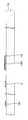
Translated fromKorean도 1은 본 발명의 실시예에 따른 표시 장치의 평면도이다.1 is a plan view of a display device according to an exemplary embodiment of the present invention.
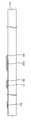
도 2는 도 1의 I-I'선을 따라 절단한 표시 장치의 단면도이다.FIG. 2 is a cross-sectional view of the display device taken along the line II ′ of FIG. 1.
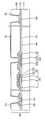
도 3 내지 도 9는 도 2에 도시된 표시 기판의 제조 방법을 나타내는 공정도들이다.3 to 9 are process diagrams illustrating a method of manufacturing the display substrate illustrated in FIG. 2.
<도면의 주요부분에 대한 부호의 설명><Description of the symbols for the main parts of the drawings>
100 : 표시 기판200 : 대향 기판100: display substrate 200: opposing substrate
CST ; 스토리지 캐패시터STE1 : 제1 스토리지 전극CST; Storage capacitor STE1: first storage electrode
STE2 : 제2 스토리지 전극126 : 게이트 배선 단부STE2: second storage electrode 126: gate wiring end
132 : 제1 게이트 절연막134 : 제2 게이트 절연막132: first gate insulating film 134: second gate insulating film
162 : 연결 패턴164 : 소스 배선 단부162: connection pattern 164: source wiring end
TFT : 스위칭 소자PE : 화소 전극TFT: switching element PE: pixel electrode
TE1 : 제1 패드 패턴TE2 : 제2 패드 패턴TE1: first pad pattern TE2: second pad pattern
GP : 게이트 패드부DP : 소스 패드부GP: Gate pad section DP: Source pad section
C1,C2,C3 : 제1, 제2, 제3 콘택홀C1, C2, C3: 1st, 2nd, 3rd contact hole
본 발명은 표시 기판과, 이의 제조 방법 및 이를 구비한 표시 장치에 관한 것으로, 보다 상세하게는 고개구율을 가지는 표시 기판과, 이의 제조 방법 및 이를 구비한 표시 장치에 관한 것이다.The present invention relates to a display substrate, a method of manufacturing the same, and a display device having the same, and more particularly, to a display substrate having a high opening ratio, a method of manufacturing the same, and a display device having the same.
일반적으로 액정표시장치(Liquid Crystal Display; LCD)는 표시 기판과 상기 표시 기판과 결합하여 액정층을 수용하는 대향 기판(Counter Substrate)을 포함한다. 상기 표시 기판에는 게이트 배선들 및 게이트 배선들과 교차하는 소스 배선들이 형성되며, 게이트 배선들과 소스 배선들에 연결된 스위칭 소자들과, 상기 스위칭 소자들에 연결된 화소 전극들이 형성된다. 각 스위칭 소자는 게이트 배선으로부터 연장된 게이트 전극, 게이트 전극과 절연되며 게이트 전극과 오버랩된 채널, 소스 배선으로부터 형성되어 채널과 전기적으로 연결된 소스 전극 및 소스 전극과 이격되며 채널과 전기적으로 연결된 드레인 전극을 포함한다.In general, a liquid crystal display (LCD) includes a display substrate and a counter substrate in combination with the display substrate to accommodate a liquid crystal layer. Gate lines and source lines intersecting the gate lines are formed on the display substrate, switching elements connected to the gate lines and the source lines, and pixel electrodes connected to the switching elements are formed. Each switching element includes a gate electrode extending from the gate wiring, a gate electrode insulated from the gate electrode, a source electrode overlapping the gate electrode, a source electrode formed from the source wiring and electrically connected to the channel, and a drain electrode spaced apart from the source electrode and electrically connected to the channel. Include.
최근 액정표시장치는 텔레비전과 같은 대형의 표시 장치는 물론, 모바일 폰, 캠코더, 디지털 카메라, MP3 플레이어 등과 같은 중소형의 표시 장치로 개발되고 있다. 이에 따라, 상기 액정표시장치는 컨텐츠의 다양화 및 고급화를 위해 고휘도가 요구되고 있으며, 이에 부응하기 위해 일 예로서, 백라이트의 휘도를 높이는 방법이 사용되고 있다. 상기와 같이 백라이트의 휘도를 높이는 방법은 소비전력을 증가시키는 단점을 갖는다.Recently, liquid crystal displays have been developed as small and medium sized display devices such as mobile phones, camcorders, digital cameras, MP3 players, as well as large display devices such as televisions. Accordingly, the liquid crystal display device requires high brightness to diversify and enhance content, and as an example, a method of increasing the brightness of a backlight is used. As described above, the method of increasing the brightness of the backlight has the disadvantage of increasing the power consumption.
이에 본 발명의 기술적 과제는 이러한 점에서 착안된 것으로, 본 발명의 목적은 고개구율을 가지는 표시 기판을 제공하는 것이다.Accordingly, the technical problem of the present invention was conceived in this respect, and an object of the present invention is to provide a display substrate having a high opening ratio.
본 발명의 다른 목적은 상기 표시 기판의 제조 방법을 제공하는 것이다.Another object of the present invention is to provide a method of manufacturing the display substrate.
본 발명의 또 다른 목적을 상기 표시 기판의 구비한 표시 장치를 제공하는 것이다.Another object of the present invention is to provide a display device provided with the display substrate.
상기한 본 발명의 목적을 실현하기 위한 실시예에 따른 표시 기판은 게이트 금속 패턴, 제1 게이트 절연막, 제2 게이트 절연막, 소스 금속 패턴 및 화소 전극을 포함한다. 상기 게이트 금속 패턴은 게이트 배선, 스위칭 소자의 게이트 전극 및 제1 스토리지 전극을 포함한다. 상기 제1 게이트 절연막은 상기 게이트 전극 및 상기 제1 스토리지 전극 중 적어도 하나를 커버한다. 상기 제2 게이트 절연막은 상기 제1 스토리지 전극 위의 제1 게이트 절연막이 노출되도록 패터닝된다. 상기 소스 금속 패턴은 소스 배선 및 상기 제1 스토리지 전극 위의 제1 게이트 절연막과 접촉하는 제2 스토리지 전극을 포함한다. 상기 화소 전극은 상기 스위칭 소자와 전기적으로 연결된다.A display substrate according to an exemplary embodiment of the present invention includes a gate metal pattern, a first gate insulating layer, a second gate insulating layer, a source metal pattern, and a pixel electrode. The gate metal pattern includes a gate wiring, a gate electrode of a switching element, and a first storage electrode. The first gate insulating layer covers at least one of the gate electrode and the first storage electrode. The second gate insulating layer is patterned to expose the first gate insulating layer on the first storage electrode. The source metal pattern includes a source wiring and a second storage electrode in contact with a first gate insulating layer on the first storage electrode. The pixel electrode is electrically connected to the switching element.
상기한 본 발명의 다른 목적을 실현하기 위한 실시예에 따른 표시 기판의 제조 방법은 베이스 기판 위에 게이트 금속층으로 게이트 배선, 스위칭 소자의 게이트 전극 및 제1 스토리지 전극을 형성하는 단계와, 상기 게이트 금속 패턴이 형성된 베이스 기판 위에 제1 게이트 절연막을 형성하는 단계와, 상기 게이트 전극 및 상기 제1 스토리지 전극 중 적어도 하나를 커버하도록 상기 제1 게이트 절연막을 패터닝하는 단계와, 상기 제1 게이트 절연막이 패터닝된 베이스 기판 위에 형성되고, 상기 제1 스토리지 전극 위의 상기 제1 게이트 절연막이 노출되도록 패터닝된 제2 게이트 절연막을 형성하는 단계와, 소스 금속층으로 소스 배선 및 상기 제1 스토리지 전극 위에 노출된 제1 게이트 절연막과 접촉되는 제1 스토리지 전극을 형성하는 단계 및 투명 도전층으로 상기 스위칭 소자와 전기적으로 연결된 화소 전극을 형성하는 단계를 포함한다.According to another aspect of the present invention, there is provided a method of manufacturing a display substrate, including forming a gate wiring, a gate electrode of a switching element, and a first storage electrode on a base substrate using a gate metal layer, and forming the gate metal pattern. Forming a first gate insulating film on the formed base substrate, patterning the first gate insulating film to cover at least one of the gate electrode and the first storage electrode, and forming a base on which the first gate insulating film is patterned. Forming a second gate insulating layer formed on a substrate and patterned to expose the first gate insulating layer on the first storage electrode, and exposing a source wiring layer and a first gate insulating layer exposed on the first storage electrode as a source metal layer; Forming a first storage electrode in contact with the transparent conductive layer To and forming a pixel electrode electrically connected with the switching element.
상기한 본 발명의 또 다른 목적을 실현하기 위한 실시예에 따른 표시 장치는 표시 기판 및 대향 기판을 포함한다. 상기 표시 기판은 스위칭 소자의 게이트 전극 및 제1 스토리지 전극 중 적어도 하나를 커버하도록 패터닝된 제1 게이트 절연막과, 상기 제1 스토리지 전극 위의 제1 게이트 절연막이 노출되도록 패터닝된 제2 게이트 절연막과, 상기 제1 스토리지 전극 위의 제1 게이트 절연막과 접촉하는 제2 스토리지 전극 및 상기 스위칭 소자와 전기적으로 연결된 화소 전극을 포함한다. 상기 대향 기판은 상기 표시 기판과 결합하여 액정층을 수용하고, 상기 화소 전극과 대향하는 공통전극이 형성된다.A display device according to an embodiment for realizing another object of the present invention described above includes a display substrate and an opposing substrate. The display substrate may include a first gate insulating layer patterned to cover at least one of a gate electrode and a first storage electrode of the switching element, a second gate insulating layer patterned to expose the first gate insulating layer on the first storage electrode; And a second storage electrode in contact with the first gate insulating layer on the first storage electrode, and a pixel electrode electrically connected to the switching element. The opposing substrate is combined with the display substrate to accommodate a liquid crystal layer, and a common electrode facing the pixel electrode is formed.
이러한 표시 기판과, 이의 제조 방법 및 이를 구비한 표시 장치에 의하면, 고개구율을 가지는 표시 기판을 구현함으로써 고휘도의 표시 영상을 얻을 수 있다.According to such a display substrate, a manufacturing method thereof, and a display device having the same, a display image having high brightness can be obtained by implementing a display substrate having a high opening ratio.
이하, 첨부한 도면들을 참조하여, 본 발명을 보다 상세하게 설명하고자 한다.Hereinafter, with reference to the accompanying drawings, it will be described in detail the present invention.
도 1은 본 발명의 실시예에 따른 표시 장치의 평면도이다. 도 2는 도 1의 I-I'선을 따라 절단한 표시 장치의 단면도이다.1 is a plan view of a display device according to an exemplary embodiment of the present invention. FIG. 2 is a cross-sectional view of the display device taken along the line II ′ of FIG. 1.
도 1 및 도 2를 참조하면, 표시 장치는 표시 기판(100)과 상기 표시 기판(100)과 결합하여 액정층(300)을 수용하는 대향 기판(200)을 포함한다. 상기 표시 기판(100)은 제1 베이스 기판(110) 위에 복수의 화소부(P)들이 매트릭스 형상으로 형성되고, 각 화소부에는 화소 전극(PE)이 형성된다. 상기 대향 기판(200)은 제2 베이스 기판(210) 위에 컬러 필터층(220)과 상기 화소 전극(PE)에 대응하는 공통 전극(230)이 형성된다.1 and 2, the display device includes a
구체적으로, 상기 표시 기판(100)은 복수의 게이트 배선(GL)들, 복수의 소스 배선(DL)들, 복수의 스위칭 소자(TFT)들, 복수의 화소 전극(PE)들 및 스토리지 캐패시터(CST)가 형성된다. 상기 스토리지 캐패시터(CST)는 공통 전압이 인가되는 스토리지 배선(SCL)과 전기적으로 연결되어 형성된다.In detail, the
상기 게이트 배선(GL)들은 게이트 금속층으로 형성되고, 제1 방향으로 연장되어 형성된다. 상기 게이트 금속층은 구리(Cu) 또는 구리 합금 등의 구리 계열 금속, 알루미늄(Al) 또는 알루미늄 합금 등 알루미늄 계열의 금속, 은(Ag) 또는 은 합금 등의 은 계열의 금속, 몰리브덴(Mo) 또는 몰리브덴 합금 등 몰리브덴 계열의 금속, 크롬(Cr), 탄탈륨(Ta) 또는 티타늄(Ti)을 포함하는 금속으로 형성되며, 단층 구조 또는 서로 다른 금속으로 적층된 다층 구조로 형성된다. 바람직하게는 저저항 금속인 알루미늄(Al)과 몰리브덴(Mo)을 포함하는 Mo/Al 다층 구조로 형성된다. The gate lines GL are formed of a gate metal layer and extend in a first direction. The gate metal layer may include a copper-based metal such as copper (Cu) or a copper alloy, an aluminum-based metal such as aluminum (Al) or an aluminum alloy, a silver-based metal such as silver (Ag) or a silver alloy, molybdenum (Mo), or molybdenum It is formed of a metal including molybdenum-based metals such as alloys, chromium (Cr), tantalum (Ta) or titanium (Ti), and is formed in a single layer structure or a multilayer structure laminated with different metals. Preferably, it is formed of a Mo / Al multilayer structure including aluminum (Al) and molybdenum (Mo), which are low resistance metals.
각 게이트 배선(GL)의 단부에는 게이트 신호가 인가되는 게이트 패드부(GP)가 형성된다. 상기 게이트 패드부(GP)는 상기 게이트 배선(GL)의 단부(126), 연결 패턴(162) 및 제1 패드 패턴(TE1)을 포함한다. 상기 게이트 배선 단부(126)는 게이 트 금속층으로 형성되고, 상기 연결 패턴(162)은 소스 금속층으로 형성되며, 상기 제1 패드 패턴(TE1)은 투명 도전층으로 형성된다.A gate pad portion GP to which a gate signal is applied is formed at an end of each gate line GL. The gate pad part GP includes an
상기 소스 배선(DL)들은 상기 소스 금속층으로 형성되고, 상기 제1 방향과 교차하는 제2 방향으로 연장되어 형성된다. 상기 소스 금속층은 구리(Cu) 또는 구리 합금 등의 구리 계열 금속, 알루미늄(Al) 또는 알루미늄 합금 등 알루미늄 계열의 금속, 은(Ag) 또는 은 합금 등의 은 계열의 금속, 몰리브덴(Mo) 또는 몰리브덴 합금 등 몰리브덴 계열의 금속, 크롬(Cr), 탄탈륨(Ta) 또는 티타늄(Ti)을 포함하는 금속으로 형성되며, 단층 구조 또는 서로 다른 금속이 적층된 다층 구조로 형성된다. 바람직하게는 몰리브덴(Mo) 또는 몰리브덴 합금 등 몰리브덴 계열의 금속으로 형성된다.The source wirings DL are formed of the source metal layer and extend in a second direction crossing the first direction. The source metal layer may be a copper-based metal such as copper (Cu) or a copper alloy, an aluminum-based metal such as aluminum (Al) or an aluminum alloy, a silver-based metal such as silver (Ag) or a silver alloy, molybdenum (Mo), or molybdenum The alloy is formed of a metal including molybdenum-based metal, chromium (Cr), tantalum (Ta), or titanium (Ti), and is formed in a single layer structure or a multilayer structure in which different metals are stacked. Preferably, it is formed of a molybdenum-based metal such as molybdenum (Mo) or molybdenum alloy.
각 소스 배선(DL)의 단부에는 소스 신호가 인가되는 소스 패드부(DP)가 형성된다. 상기 소스 패드부(DP)는 상기 소스 배선(DL)의 단부(164)와 제2 패드 패턴(TE2)을 포함한다. 상기 소스 배선 단부(164)는 상기 소스 금속층으로 형성되고, 상기 제2 패드 패턴(TE2)은 상기 투명 도전층으로 형성된다.A source pad part DP to which a source signal is applied is formed at an end of each source wiring DL. The source pad part DP includes an
상기 스위칭 소자(TFT)들은 상기 게이트 배선(GL)들과 소스 배선(DL)들에 의해 정의된 복수의 화소부(P)들에 각각 형성된다. 각 스위칭 소자(TFT)는 해당하는 게이트 배선(GL)과 연결된 게이트 전극(G)과, 해당하는 소스 배선(DL)과 연결된 소스 전극(S) 및 상기 소스 전극(S)과 이격되어 채널부(140)를 통해 전기적으로 연결된 드레인 전극(D)을 포함한다. 상기 게이트 전극(G)과 채널부(140) 사이에는 제1 게이트 절연막(132) 및 제2 게이트 절연막(134) 중 적어도 하나의 절연막이 형성된 다. 바람직하게 상기 제1 및 제2 게이트 절연막(132, 134)이 순차적으로 적층되어 형성되거나, 상기 제2 게이트 절연막(132)이 단층으로 형성된다. 상기 제1 게이트 절연막(132)은 산화 실리콘(SiOx)으로 대략 500Å 내지 1200Å정도의 두께로 형성되고, 상기 제2 게이트 절연막(134)은 질화 실리콘(SiNx)으로 형성되며, 대략 3000Å 내지 4500Å정도의 두께로 형성된다. 여기서는 상기 게이트 전극(G)과 채널부(140) 사이에 제2 게이트 절연막(134)이 형성된 것을 도시하고 있다.The switching elements TFT are formed in the plurality of pixel portions P defined by the gate lines GL and the source lines DL, respectively. Each switching element TFT is spaced apart from the gate electrode G connected to the corresponding gate line GL, the source electrode S connected to the corresponding source line DL, and the source electrode S, And a drain electrode D electrically connected through the 140. At least one insulating layer of the first
상기 화소 전극(PE)들은 상기 스위칭 소자(TFT)들과 전기적으로 연결된다. 각 화소 전극(PE)은 해당하는 스위칭 소자(TFT)의 드레인 전극(DE)과 전기적으로 연결되어 상기 화소부(P)에 형성된다. 상기 화소 전극(PE)은 상기 투명 도전층으로 형성된다. 상기 투명 도전층은 인듐(In), 주석(Sn), 아연(Zn), 알루미늄(Al) 및 갈륨(Ga) 중 선택된 하나 이상을 함유한 산화물질 또는 질산화물질로 형성된다.The pixel electrodes PE are electrically connected to the switching elements TFTs. Each pixel electrode PE is electrically connected to the drain electrode DE of the corresponding switching element TFT and is formed in the pixel portion P. The pixel electrode PE is formed of the transparent conductive layer. The transparent conductive layer is formed of an oxide or nitride oxide containing at least one selected from indium (In), tin (Sn), zinc (Zn), aluminum (Al), and gallium (Ga).
상기 스토리지 캐패시터(CST)는 공통전압이 인가되는 스토리지 배선(STL)과 연결된 제1 스토리지 전극(STE1)과, 제1 게이트 절연막(132) 및 상기 제1 스토리지 전극(STE1)과 마주하는 제2 스토리지 전극(STE2)을 포함한다.The storage capacitor CST has a first storage electrode STE1 connected to a storage line STL to which a common voltage is applied, a first
상기 제1 스토리지 전극(STE1)은 상기 게이트 금속층으로 형성되고, 상기 제2 스토리지 전극(STE2)은 상기 소스 금속층으로 형성된다. 상기 제1 게이트 절연막(132)은 절연 특성이 우수한 절연물질로 상기 제2 게이트 절연막(134) 보다 얇은 두께로 형성된다.바람직하게 상기 제1 게이트 절연막(132)은 산화 실리콘(SiOx)으로 대략 500Å 내지 1200Å정도의 두께로 형성된다.The first storage electrode STE1 is formed of the gate metal layer, and the second storage electrode STE2 is formed of the source metal layer. The first
상기 스토리지 캐패시터(CST)의 커패시턴스(Cstg)는 다음의 수학식 1과 같이 정의된다.The capacitance Cstg of the storage capacitor CST is defined as in Equation 1 below.

여기서, A는 상기 제1 스토리지 전극(STE1)의 면적이고, d는 상기 제1 및 제2 스토리지 전극들(STE1, STE2) 간의 거리이고, ε은 유전체의 유전율이다. 즉, 상기 d는 상기 제1 게이트 절연막(132)의 두께이고, 상기 ε은 상기 제1 게이트 절연막(132)의 유전율이다.Here, A is the area of the first storage electrode STE1, d is the distance between the first and second storage electrodes STE1 and STE2, and ε is the dielectric constant of the dielectric. That is, d is a thickness of the first
상기 수학식 1을 참고할 때, 상기 스토리지 캐패시터(CST)는 제1 및 제2 스토리지 전극들(STE1, STE2) 간의 간격(d)을 얇게 형성하는 경우, 상기 제1 스토리지 전극(STE1)의 면적(A)을 작게 형성하여도 실질적으로 충분한 커패시턴스(Cstg)를 얻을 수 있다.Referring to Equation 1, when the storage capacitor CST forms a thin gap d between the first and second storage electrodes STE1 and STE2, the area of the first storage electrode STE1 is reduced. Even if A) is made small, substantially sufficient capacitance Cstg can be obtained.
이와 같은 원리에 따라서, 상기 제1 게이트 절연막을 산화 실리콘(SiO2)으로 대략 500Å 내지 1200Å정도의 두께로 형성함으로써 상기 제1 스토리지 전극(STE1)의 면적을 줄여 개구율을 향상시킨다.According to this principle, the first gate insulating layer is formed of silicon oxide (SiO 2) to a thickness of about 500 GPa to 1200 GPa to reduce the area of the first storage electrode STE 1 to improve the aperture ratio.
다음의 표 1은 스토리지 캐패시터의 두께(d)에 따른 면적(A)의 감소율을 나타낸 것이다.Table 1 below shows the reduction rate of the area A according to the thickness d of the storage capacitor.
상기 표 1을 참조하면, 비교예 1의 스토리지 캐패시터는 양단 전극이 게이트 금속층과 투명 도전층으로 형성되고, 유전체는 게이트 절연막과 패시베이션막으로 대략 6000Å의 두께로 형성된다. 상기 비교예 1의 스토리지 캐패시터는 화소부 면적의 대략 20% 정도로 형성된다.Referring to Table 1, in the storage capacitor of Comparative Example 1, both electrodes are formed of a gate metal layer and a transparent conductive layer, and a dielectric material is formed with a thickness of approximately 6000 mW with a gate insulating film and a passivation film. The storage capacitor of Comparative Example 1 is formed to about 20% of the area of the pixel portion.
상기 비교예 2의 스토리지 캐패시터는 양단 전극이 게이트 금속층과 소스 금속층으로 형성되고, 유전체는 게이트 절연막으로 대략 4000Å의 두께로 형성되는 경우이다. 상기 비교예 2의 스토리지 캐패시터는 유전체의 두께가 비교예 1에 비해 대략 2000Å으로 얇게 형성된다. 이에 따라서 상기 비교예 2의 스토리지 캐패시터는 화소부 면적의 대략 16% 정도로 형성된다. 비교예 2의 스토리지 캐패시터 면적은 비교예 1의 스토리지 캐패시터 면적에 비해 대략 20% 정도 감소된다.The storage capacitor of Comparative Example 2 is a case where both electrodes are formed of a gate metal layer and a source metal layer, and the dielectric is formed with a gate insulating film having a thickness of approximately 4000 kPa. In the storage capacitor of Comparative Example 2, the thickness of the dielectric is approximately 2000 kHz thinner than that of Comparative Example 1. Accordingly, the storage capacitor of Comparative Example 2 is formed to about 16% of the area of the pixel portion. The storage capacitor area of Comparative Example 2 is reduced by approximately 20% compared to the storage capacitor area of Comparative Example 1.
본 발명의 실시예에 따른 스토리지 캐패시터는 양단 전극이 게이트 금속층과 소스 금속층으로 형성되고, 대략 750Å 두께의 게이트 절연막으로 유전체가 형성된다. 이 경우, 상기 실시예의 스토리지 캐패시터 면적은 화소부 면적의 대략 4% 정도로 형성된다. 따라서, 상기 실시예의 스토리지 캐패시터 면적은 상기 비교예 1의 면적에 비해 대략 80% 정도로 감소되고, 상기 비교예 2의 면적에 비해 대략 75% 정도 감소된다.In the storage capacitor according to the exemplary embodiment of the present invention, both electrodes are formed of a gate metal layer and a source metal layer, and a dielectric is formed of a gate insulating film having a thickness of approximately 750 Å. In this case, the storage capacitor area of the embodiment is formed at about 4% of the area of the pixel portion. Therefore, the storage capacitor area of the embodiment is reduced by about 80% compared to the area of Comparative Example 1, and is reduced by about 75% compared to the area of Comparative Example 2.
이와 같이, 스토리지 캐패시터(CST)의 면적(A)은 유전체의 두께(d)가 얇을수록 작아진다.As described above, the area A of the storage capacitor CST decreases as the thickness d of the dielectric decreases.
따라서, 상기 스토리지 캐패시터(CST)의 면적은 상기 스토리지 캐패시터(CST)의 유전체인 상기 제1 게이트 절연막(132)의 두께를 얇게 형성하여 스토리지 캐패시터의 면적을 작게 형성하여 고개구율을 구현한다. 예컨대, 상기 제1 게이트 절연막(132)의 두께를 얇게 형성함에 따라서 상기 스토리지 캐패시터(CST)의 면적을 상기 화소부(P) 면적의 3% 내지 10% 정도로 형성 가능하다.Therefore, the area of the storage capacitor CST is formed to have a small thickness of the first
도 3 내지 도 9는 도 1에 도시된 표시 기판의 제조 방법을 나타낸 공정도들이다.3 to 9 are process diagrams illustrating a method of manufacturing the display substrate illustrated in FIG. 1.
도 1 및 도 3을 참조하면, 제1 베이스 기판(110) 위에 게이트 금속층을 증착 및 패터닝하여 게이트 금속 패턴을 형성한다.1 and 3, the gate metal layer is deposited and patterned on the
상기 게이트 금속 패턴은 게이트 배선(GL), 스위칭 소자(TFT)의 게이트 전극(G), 스토리지 배선(STL) 및 상기 스토리지 배선(STL)에 연결된 제1 스토리지 전극(STE1)을 포함한다. 상기 게이트 배선(GL)은 게이트 패드부(GP)가 형성되는 게이트 배선 단부(126)를 포함한다The gate metal pattern includes a gate line GL, a gate electrode G of a switching element TFT, a storage line STL, and a first storage electrode STE1 connected to the storage line STL. The gate line GL includes a
상기 게이트 금속 패턴이 형성된 제1 베이스 기판(110) 위에 제1 두께(d)로 제1 게이트 절연막(132)을 형성한다. 상기 제1 게이트 절연막(132)은 절연특성이 우수한 절연물질로 대략 500Å 내지 1200Å의 제1 두께(d1)로 형성된다. 바람직하게 상기 제1 게이트 절연막(132)은 산화 실리콘(SiO2)으로 형성된다.The first
도 1, 도 4a 및 도 4b를 참조하면, 상기 제1 게이트 절연막(132)을 상기 게이트 전극(G) 및 제1 스토리지 전극(STE1) 중 적어도 하나를 커버하도록 패터닝한다.1, 4A, and 4B, the first
바람직한 일 예로서, 도 4a에 도시된 바와 같이, 상기 제1 게이트 절연막(132)은 상기 제1 스토리지 전극(SE1) 만을 커버하도록 패터닝한다.As a preferred example, as illustrated in FIG. 4A, the first
상기 게이트 금속 패턴을 저저항의 Mo/Al 구조로 형성하는 경우, 접착성은 우수하나 상대적으로 내막성이 떨어지는 몰리브덴은 상기 제1 게이트 절연막(132) 패터닝 공정에서 손상될 수 있다. 즉, 대략 500Å 내지 1200Å의 얇은 두께로 형성된 상기 제1 게이트 절연막(132)을 식각하는 공정에서 상기 제1 게이트 절연막(132)이 패터닝되어 노출된 상기 게이트 금속 패턴에 손상이 발생될 수 있다. 이러한 게이트 금속 패턴의 손상으로 인해 게이트 패드부(GP)의 전기적 특성이 저하되는 불량을 방지하기 위해 상기 게이트 배선 단부(126)와 접촉되는 연결 패턴(162)을 추후 소스 금속 패턴 형성공정에서 형성한다.When the gate metal pattern is formed of a low-resistance Mo / Al structure, molybdenum having excellent adhesion but relatively low film resistance may be damaged in the first
바람직한 다른 예로서, 도 4b에 도시된 바와 같이, 상기 제1 게이트 절연막(132)은 상기 게이트 전극(G) 및 제1 스토리지 전극(STE1)을 각각 커버하도록 패터닝한다. 즉, 상기 제1 스토리지 전극(STE1) 위에는 상기 제1 게이트 절연막(132)을 형성하고, 상기 게이트 전극(G) 위에는 상기 제1 게이트 절연막(132)을 선택적으로 형성할 수 있다.As another preferred example, as illustrated in FIG. 4B, the first
이하에서는 도 4a에 도시된 바와 같이, 상기 제1 게이트 절연막(132)이 상기 제1 스토리지 전극(STE1) 위에 형성된 경우를 예로 하여 설명한다.Hereinafter, as illustrated in FIG. 4A, a case in which the first
도 1 및 도 5를 참조하면, 상기 제1 게이트 절연막(132)이 상기 제1 스토리지 전극(STE1) 위에 형성된 제1 베이스 기판(110) 위에 제2 두께(d2)로 제2 게이트 절연막(134)을 형성한다. 상기 제2 게이트 절연막(134)은 질화 실리콘(SiNx)으로 대략 3000Å 내지 4500Å의 제2 두께(d2)로 형성된다.1 and 5, the first
상기 제2 게이트 절연막(134)이 형성된 제1 베이스 기판(110) 위에 채널층(140)을 형성한다. 상기 채널층(140)은 순차적으로 적층된 비정질 실리콘(a-Si)으로 형성된 활성층(142)과, n+ 이온이 고농도로 도핑된 비정질 실리콘(n+ a-Si)으로 형성된 저항성 접촉층(144)을 포함한다.The
도 1, 도 6a 및 도 6b를 참조하면, 상기 채널층(140)을 패터닝하여 상기 게이트 전극(G) 위의 제2 게이트 절연막(134) 위에 상기 채널층(140)을 잔류시킨다.1, 6A and 6B, the
이어, 상기 제2 게이트 절연막(134)을 패터닝하여 상기 제1 스토리지 전극(STE1) 위에 제1 게이트 절연막(132)을 노출시키고, 상기 게이트 배선 단부(126)를 노출시킨다. 이때, 상기 제1 게이트 절연막(132)과 상기 제2 게이트 절연막(134)은 서로 다른 식각 선택비를 갖는다. 이에 의해 상기 제1 게이트 절연막(132)은 식각하지 않고, 상기 제2 게이트 절연막(134)만 식각된다.Subsequently, the second
일 예로서, 도 6a에 도시된 바와 같이 상기 제2 게이트 절연막(134)을 상기 제1 스토리지 전극(STE1) 및 상기 단부(126) 각각의 가장자리와 중첩되도록 패터닝한다. 또는, 다른 예로서 도 6b에 도시된 바와 같이 상기 제1 스토리지 전극(STE1) 및 상기 단부(126)와 중첩되는 영역이 존재하지 않도록 패터닝한다. 여기서는 상기 제1 스토리지 전극(STE1) 및 상기 단부(126) 각각의 가장자리와 중첩되는 영역이 존재하도록 상기 제2 게이트 절연막(134)이 패터닝된 것을 예로서 설명한다.For example, as illustrated in FIG. 6A, the second
도 1 및 도 7을 참조하면, 상기 제2 게이트 절연막(134)이 패터닝된 제1 베이스 기판(110) 위에 소스 금속층을 증착 및 패터닝하여 소스 금속 패턴을 형성한다.1 and 7, a source metal pattern is formed by depositing and patterning a source metal layer on the
상기 소스 금속 패턴은 상기 소스 배선(DL)과, 상기 스위칭 소자(TFT)의 소스 전극(S) 및 드레인 전극(D)과, 상기 스토리지 캐패시터(CST)의 제2 스토리지 전극(STE2) 및 상기 게이트 패드부(GP)의 연결 패턴(162)을 포함한다. 상기 제2 스토리지 전극(STE2)은 상기 제1 스토리지 전극(STE1) 위의 제1 게이트 절연막(132)과 접촉된다. 상기 연결 패턴(162)은 상기 게이트 배선 단부(126)와 접촉되어 상기 게이트 패드부(GP)의 전기적 특성을 향상시킨다. 상기 소스 배선(DL)은 상기 소스 패드부(DP)가 형성되는 소스 배선 단부(164)를 포함한다.The source metal pattern may include the source wiring DL, the source electrode S and the drain electrode D of the switching element TFT, the second storage electrode STE2 of the storage capacitor CST, and the gate. The
이 후, 상기 소스 금속 패턴을 마스크로 하여 상기 소스 전극(S) 및 드레인 전극(D) 사이에 노출된 상기 저항성 접촉층(144)을 식각하여 상기 스위칭 소자(TFT)의 채널을 형성한다.Thereafter, the
이에 의해 상기 스토리지 캐패시터(CST)는 제1 스토리지 전극(STE1)과 제2 스토리지 전극(STE2) 및 상기 제1 및 제2 스토리지 전극들(STE1, STE2) 사이에 개재된 제1 게이트 절연막(132)으로 정의된다.As a result, the storage capacitor CST includes the first
도 1 및 도 8을 참조하면, 상기 소스 금속 패턴이 형성된 제1 베이스 기판(110) 위에 패시베이션막(170) 및 유기막(180)을 순차적으로 형성한다. 상기 패시베이션막(170)은 대략 2000Å 정도의 두께로 형성되며, 질화 실리콘(SiNx) 또는 산화 실리콘(SiO2)으로 형성된다.1 and 8, the
이 후, 상기 유기막(180) 및 패시베이션막(170)을 패터닝하여, 상기 제2 스토리지 전극(STE2)을 노출시키는 제1 콘택홀(C1)과, 상기 게이트 패드부(GP)의 연결 패턴(162)을 노출시키는 제2 콘택홀(C2) 및 상기 소스 패드부(DP)의 소스 배선 단부(164)를 노출시키는 제3 콘택홀(C3)을 형성한다.Thereafter, the
도 1 및 도 9를 참조하면, 상기 제1 내지 제3 콘택홀들(C1, C2, C3)이 형성된 제1 베이스 기판(110) 위에 투명 도전층을 증착 및 패터닝하여 투명 전극패턴을 형성한다. 상기 투명 전극패턴은 상기 제1 콘택홀(C1)을 통해 상기 제2 스토리지 전극(STE2)과 접촉하는 화소 전극(PE)과, 상기 제2 콘택홀(C2)을 통해 상기 연결 패턴(162)과 접촉하는 제1 패드 패턴(TE1) 및 상기 제3 콘택홀(C3)을 통해 상기 소스 배선 단부(164)와 접촉하는 제2 패드 패턴(TE2)을 포함한다.1 and 9, a transparent conductive layer is deposited and patterned on the
이상에서 설명한 바와 같이, 본 발명에 따르면 게이트 절연층을 식각 선택비가 서로 다른 제1 게이트 절연막과 제2 게이트 절연막의 다층 구조로 형성하고, 상기 제1 게이트 절연막은 얇은 두께로 스토리지 캐패시터의 유전체로 적용하며, 상기 제2 게이트 절연막은 게이트 전극을 전기적으로 절연하는 절연층으로 적용한다. 여기서 제1 게이트 절연막을 얇은 두께로 형성하고, 제2 게이트 절연막은 기존 게이트 절연층의 두께로 형성한다.As described above, according to the present invention, the gate insulating layer is formed in a multilayer structure of a first gate insulating layer and a second gate insulating layer having different etching selectivity, and the first gate insulating layer is applied to the dielectric of the storage capacitor with a thin thickness. The second gate insulating layer is applied as an insulating layer electrically insulating the gate electrode. Here, the first gate insulating film is formed to a thin thickness, and the second gate insulating film is formed to a thickness of the existing gate insulating layer.
구체적으로, 상기 스토리지 캐패시터의 제1 전극을 게이트 금속층으로 형성하고, 제2 전극을 소스 금속층으로 형성하고, 상기 제1 및 제2 전극 사이에 얇은 두께의 제1 게이트 절연막을 형성하여 화소부 내의 상기 스토리지 캐패시터의 점유 면적을 감소시켜 고개구율의 표시 기판을 구현할 수 있다.Specifically, the first electrode of the storage capacitor is formed of a gate metal layer, the second electrode is formed of a source metal layer, and a thin first gate insulating film is formed between the first and second electrodes to form the By reducing the area occupied by the storage capacitor, a display substrate having a high opening ratio can be realized.
한편, 상기 제2 게이트 절연막을 상기 게이트 전극을 전기적으로 절연시키는 절연층을 사용함으로써 상기 스위칭 소자의 전기적 특성은 유지하면서 고개구율을 도모할 수 있다.On the other hand, by using the second gate insulating film as an insulating layer that electrically insulates the gate electrode, it is possible to achieve a high opening ratio while maintaining the electrical characteristics of the switching element.
이상에서는 실시예를 참조하여 설명하였지만, 해당 기술 분야의 숙련된 당업자는 하기의 특허 청구의 범위에 기재된 본 발명의 사상 및 영역으로부터 벗어나지 않는 범위 내에서 본 발명을 다양하게 수정 및 변경시킬 수 있음을 이해할 수 있을 것이다.Although described above with reference to the embodiments, those skilled in the art can be variously modified and changed within the scope of the invention without departing from the spirit and scope of the invention described in the claims below. I can understand.
Claims (17)
Translated fromKoreanPriority Applications (3)
| Application Number | Priority Date | Filing Date | Title |
|---|---|---|---|
| KR1020060041807AKR20070109192A (en) | 2006-05-10 | 2006-05-10 | Display substrate, manufacturing method thereof and display device having same |
| CNA2007100798153ACN101071242A (en) | 2006-05-10 | 2007-02-14 | Display substrate, method for manufacturing the same and display apparatus having the same |
| US11/697,983US20070262347A1 (en) | 2006-05-10 | 2007-04-09 | Display substrate, method for manufacturing the same and display apparatus having the same |
Applications Claiming Priority (1)
| Application Number | Priority Date | Filing Date | Title |
|---|---|---|---|
| KR1020060041807AKR20070109192A (en) | 2006-05-10 | 2006-05-10 | Display substrate, manufacturing method thereof and display device having same |
Publications (1)
| Publication Number | Publication Date |
|---|---|
| KR20070109192Atrue KR20070109192A (en) | 2007-11-15 |
Family
ID=38684301
Family Applications (1)
| Application Number | Title | Priority Date | Filing Date |
|---|---|---|---|
| KR1020060041807ACeasedKR20070109192A (en) | 2006-05-10 | 2006-05-10 | Display substrate, manufacturing method thereof and display device having same |
Country Status (3)
| Country | Link |
|---|---|
| US (1) | US20070262347A1 (en) |
| KR (1) | KR20070109192A (en) |
| CN (1) | CN101071242A (en) |
Cited By (2)
| Publication number | Priority date | Publication date | Assignee | Title |
|---|---|---|---|---|
| KR101113354B1 (en)* | 2010-04-16 | 2012-02-29 | 삼성모바일디스플레이주식회사 | Display device and fabrication method of the same |
| KR101335527B1 (en)* | 2012-02-23 | 2013-12-02 | 엘지디스플레이 주식회사 | Organic Light Emitting Diode Display Device and Method for Manufacturing The Same |
Families Citing this family (6)
| Publication number | Priority date | Publication date | Assignee | Title |
|---|---|---|---|---|
| KR101353269B1 (en)* | 2006-12-11 | 2014-01-20 | 삼성디스플레이 주식회사 | Thin film transistor substrate and method for manufacturing the same |
| JP2009122376A (en)* | 2007-11-14 | 2009-06-04 | Hitachi Displays Ltd | Display device |
| KR101670695B1 (en) | 2008-09-19 | 2016-10-31 | 가부시키가이샤 한도오따이 에네루기 켄큐쇼 | Semiconductor device |
| KR20120042029A (en)* | 2010-10-22 | 2012-05-03 | 삼성모바일디스플레이주식회사 | Display device and method for manufacturing the same |
| CN103296034A (en)* | 2013-05-28 | 2013-09-11 | 京东方科技集团股份有限公司 | Array substrate, production method thereof and display device |
| KR102031203B1 (en)* | 2019-03-20 | 2019-10-11 | 동우 화인켐 주식회사 | Antenna laminate and image display device including the same |
Family Cites Families (10)
| Publication number | Priority date | Publication date | Assignee | Title |
|---|---|---|---|---|
| KR970011972A (en)* | 1995-08-11 | 1997-03-29 | 쯔지 하루오 | Transmission type liquid crystal display device and manufacturing method thereof |
| JP3980156B2 (en)* | 1998-02-26 | 2007-09-26 | 株式会社半導体エネルギー研究所 | Active matrix display device |
| EP1049167A3 (en)* | 1999-04-30 | 2007-10-24 | Sel Semiconductor Energy Laboratory Co., Ltd. | Semiconductor device and manufacturing method thereof |
| KR100720434B1 (en)* | 2000-09-27 | 2007-05-22 | 엘지.필립스 엘시디 주식회사 | LCD and its manufacturing method |
| KR100392850B1 (en)* | 2000-12-29 | 2003-07-28 | 엘지.필립스 엘시디 주식회사 | Liquid Crystal Display Device and Fabricating Method Thereof |
| JP4306142B2 (en)* | 2001-04-24 | 2009-07-29 | 株式会社日立製作所 | Image display device and manufacturing method thereof |
| JP4108078B2 (en)* | 2004-01-28 | 2008-06-25 | シャープ株式会社 | Active matrix substrate and display device |
| JP4088619B2 (en)* | 2004-01-28 | 2008-05-21 | シャープ株式会社 | Active matrix substrate and display device |
| EP1837842B1 (en)* | 2004-12-16 | 2014-01-22 | Sharp Kabushiki Kaisha | Active matrix substrate, method for manufacturing active matrix substrate, display, liquid crystal display and television system |
| KR20060090523A (en)* | 2005-02-07 | 2006-08-11 | 삼성전자주식회사 | Display device wiring and thin film transistor display panel including the wiring |
- 2006
- 2006-05-10KRKR1020060041807Apatent/KR20070109192A/ennot_activeCeased
- 2007
- 2007-02-14CNCNA2007100798153Apatent/CN101071242A/enactivePending
- 2007-04-09USUS11/697,983patent/US20070262347A1/ennot_activeAbandoned
Cited By (4)
| Publication number | Priority date | Publication date | Assignee | Title |
|---|---|---|---|---|
| KR101113354B1 (en)* | 2010-04-16 | 2012-02-29 | 삼성모바일디스플레이주식회사 | Display device and fabrication method of the same |
| US8988640B2 (en) | 2010-04-16 | 2015-03-24 | Samsung Display Co., Ltd. | Display device and fabrication method of the same |
| KR101335527B1 (en)* | 2012-02-23 | 2013-12-02 | 엘지디스플레이 주식회사 | Organic Light Emitting Diode Display Device and Method for Manufacturing The Same |
| US8680517B2 (en) | 2012-02-23 | 2014-03-25 | Lg Display Co., Ltd. | Organic light emitting diode display device and method of manufacturing the same |
Also Published As
| Publication number | Publication date |
|---|---|
| CN101071242A (en) | 2007-11-14 |
| US20070262347A1 (en) | 2007-11-15 |
Similar Documents
| Publication | Publication Date | Title |
|---|---|---|
| CN1858911B (en) | Tft array panel, liquid crystal display including same, and method of manufacturing tft array panel | |
| KR101353269B1 (en) | Thin film transistor substrate and method for manufacturing the same | |
| US7336324B2 (en) | Array substrate for liquid crystal display device and fabricating method thereof | |
| CN112071860B (en) | Active matrix substrate and method for manufacturing same | |
| US20060273316A1 (en) | Array substrate having enhanced aperture ratio, method of manufacturing the same and display apparatus having the same | |
| KR20070109192A (en) | Display substrate, manufacturing method thereof and display device having same | |
| KR101192626B1 (en) | Display substrate, method of manufacturing thereof and display apparatus having the same | |
| CN102191467B (en) | Metal line, film-forming method, tft array panel and manufacture method thereof | |
| EP3118675B1 (en) | Ultra high density thin film transistor substrate having low line resistance structure and method for manufacturing the same | |
| US20150287799A1 (en) | Semiconductor device, display panel, and semiconductor device manufacturing method | |
| EP2743984A2 (en) | Array substrate and the method for manufacturing the same, and liquid crystal display device | |
| CN1963649B (en) | Thin film transistor array panel for liquid crystal display and its manufacture method | |
| JP2007250804A (en) | Thin film transistor substrate and manufacturing method thereof | |
| US8111342B2 (en) | Display substrate, method of manufacturing the same and display device using the display substrate | |
| US20160035750A1 (en) | Thin film transistor array panel and manufacturing method thereof | |
| KR20060097381A (en) | Thin film transistor substrate and manufacturing method thereof | |
| TWI479574B (en) | TFT array substrate and manufacturing method thereof | |
| JP2009265662A (en) | High-aperture-ratio array substrate, liquid crystal display device, and manufacturing methods thereof | |
| US20070249096A1 (en) | Method of Forming a Metal Line and Method of Manufacturing a Display Substrate by Using the Same | |
| KR20090078527A (en) | Display board | |
| US7960219B2 (en) | Thin-film transistor substrate and method of fabricating the same | |
| US20090191698A1 (en) | Tft array panel and fabricating method thereof | |
| US8299468B2 (en) | Display substrate having reduced defects | |
| CN101989579A (en) | TFT array substrate and manufacturing method thereof | |
| JP4084630B2 (en) | Liquid crystal display |
Legal Events
| Date | Code | Title | Description |
|---|---|---|---|
| PA0109 | Patent application | Patent event code:PA01091R01D Comment text:Patent Application Patent event date:20060510 | |
| PG1501 | Laying open of application | ||
| A201 | Request for examination | ||
| PA0201 | Request for examination | Patent event code:PA02012R01D Patent event date:20110509 Comment text:Request for Examination of Application Patent event code:PA02011R01I Patent event date:20060510 Comment text:Patent Application | |
| E902 | Notification of reason for refusal | ||
| PE0902 | Notice of grounds for rejection | Comment text:Notification of reason for refusal Patent event date:20120709 Patent event code:PE09021S01D | |
| E601 | Decision to refuse application | ||
| PE0601 | Decision on rejection of patent | Patent event date:20120915 Comment text:Decision to Refuse Application Patent event code:PE06012S01D Patent event date:20120709 Comment text:Notification of reason for refusal Patent event code:PE06011S01I |