KR20070107694A - Illumination device - Google Patents
Illumination deviceDownload PDFInfo
- Publication number
- KR20070107694A KR20070107694AKR1020077018092AKR20077018092AKR20070107694AKR 20070107694 AKR20070107694 AKR 20070107694AKR 1020077018092 AKR1020077018092 AKR 1020077018092AKR 20077018092 AKR20077018092 AKR 20077018092AKR 20070107694 AKR20070107694 AKR 20070107694A
- Authority
- KR
- South Korea
- Prior art keywords
- optical element
- optoelectronic component
- semiconductor chip
- radiation
- optical
- Prior art date
- Legal status (The legal status is an assumption and is not a legal conclusion. Google has not performed a legal analysis and makes no representation as to the accuracy of the status listed.)
- Granted
Links
Images


Classifications
- H—ELECTRICITY
- H10—SEMICONDUCTOR DEVICES; ELECTRIC SOLID-STATE DEVICES NOT OTHERWISE PROVIDED FOR
- H10H—INORGANIC LIGHT-EMITTING SEMICONDUCTOR DEVICES HAVING POTENTIAL BARRIERS
- H10H20/00—Individual inorganic light-emitting semiconductor devices having potential barriers, e.g. light-emitting diodes [LED]
- H10H20/80—Constructional details
- H10H20/85—Packages
- H10H20/855—Optical field-shaping means, e.g. lenses
- F—MECHANICAL ENGINEERING; LIGHTING; HEATING; WEAPONS; BLASTING
- F21—LIGHTING
- F21V—FUNCTIONAL FEATURES OR DETAILS OF LIGHTING DEVICES OR SYSTEMS THEREOF; STRUCTURAL COMBINATIONS OF LIGHTING DEVICES WITH OTHER ARTICLES, NOT OTHERWISE PROVIDED FOR
- F21V5/00—Refractors for light sources
- F21V5/04—Refractors for light sources of lens shape
- H—ELECTRICITY
- H10—SEMICONDUCTOR DEVICES; ELECTRIC SOLID-STATE DEVICES NOT OTHERWISE PROVIDED FOR
- H10H—INORGANIC LIGHT-EMITTING SEMICONDUCTOR DEVICES HAVING POTENTIAL BARRIERS
- H10H20/00—Individual inorganic light-emitting semiconductor devices having potential barriers, e.g. light-emitting diodes [LED]
- H10H20/80—Constructional details
- H10H20/85—Packages
- F—MECHANICAL ENGINEERING; LIGHTING; HEATING; WEAPONS; BLASTING
- F21—LIGHTING
- F21Y—INDEXING SCHEME ASSOCIATED WITH SUBCLASSES F21K, F21L, F21S and F21V, RELATING TO THE FORM OR THE KIND OF THE LIGHT SOURCES OR OF THE COLOUR OF THE LIGHT EMITTED
- F21Y2115/00—Light-generating elements of semiconductor light sources
- F21Y2115/10—Light-emitting diodes [LED]
- H—ELECTRICITY
- H01—ELECTRIC ELEMENTS
- H01L—SEMICONDUCTOR DEVICES NOT COVERED BY CLASS H10
- H01L2224/00—Indexing scheme for arrangements for connecting or disconnecting semiconductor or solid-state bodies and methods related thereto as covered by H01L24/00
- H01L2224/01—Means for bonding being attached to, or being formed on, the surface to be connected, e.g. chip-to-package, die-attach, "first-level" interconnects; Manufacturing methods related thereto
- H01L2224/26—Layer connectors, e.g. plate connectors, solder or adhesive layers; Manufacturing methods related thereto
- H01L2224/31—Structure, shape, material or disposition of the layer connectors after the connecting process
- H01L2224/32—Structure, shape, material or disposition of the layer connectors after the connecting process of an individual layer connector
- H01L2224/321—Disposition
- H01L2224/32151—Disposition the layer connector connecting between a semiconductor or solid-state body and an item not being a semiconductor or solid-state body, e.g. chip-to-substrate, chip-to-passive
- H01L2224/32221—Disposition the layer connector connecting between a semiconductor or solid-state body and an item not being a semiconductor or solid-state body, e.g. chip-to-substrate, chip-to-passive the body and the item being stacked
- H01L2224/32245—Disposition the layer connector connecting between a semiconductor or solid-state body and an item not being a semiconductor or solid-state body, e.g. chip-to-substrate, chip-to-passive the body and the item being stacked the item being metallic
- H—ELECTRICITY
- H01—ELECTRIC ELEMENTS
- H01L—SEMICONDUCTOR DEVICES NOT COVERED BY CLASS H10
- H01L2224/00—Indexing scheme for arrangements for connecting or disconnecting semiconductor or solid-state bodies and methods related thereto as covered by H01L24/00
- H01L2224/01—Means for bonding being attached to, or being formed on, the surface to be connected, e.g. chip-to-package, die-attach, "first-level" interconnects; Manufacturing methods related thereto
- H01L2224/42—Wire connectors; Manufacturing methods related thereto
- H01L2224/47—Structure, shape, material or disposition of the wire connectors after the connecting process
- H01L2224/48—Structure, shape, material or disposition of the wire connectors after the connecting process of an individual wire connector
- H01L2224/4805—Shape
- H01L2224/4809—Loop shape
- H01L2224/48091—Arched
- H—ELECTRICITY
- H01—ELECTRIC ELEMENTS
- H01L—SEMICONDUCTOR DEVICES NOT COVERED BY CLASS H10
- H01L2224/00—Indexing scheme for arrangements for connecting or disconnecting semiconductor or solid-state bodies and methods related thereto as covered by H01L24/00
- H01L2224/01—Means for bonding being attached to, or being formed on, the surface to be connected, e.g. chip-to-package, die-attach, "first-level" interconnects; Manufacturing methods related thereto
- H01L2224/42—Wire connectors; Manufacturing methods related thereto
- H01L2224/47—Structure, shape, material or disposition of the wire connectors after the connecting process
- H01L2224/48—Structure, shape, material or disposition of the wire connectors after the connecting process of an individual wire connector
- H01L2224/481—Disposition
- H01L2224/48151—Connecting between a semiconductor or solid-state body and an item not being a semiconductor or solid-state body, e.g. chip-to-substrate, chip-to-passive
- H01L2224/48221—Connecting between a semiconductor or solid-state body and an item not being a semiconductor or solid-state body, e.g. chip-to-substrate, chip-to-passive the body and the item being stacked
- H01L2224/48245—Connecting between a semiconductor or solid-state body and an item not being a semiconductor or solid-state body, e.g. chip-to-substrate, chip-to-passive the body and the item being stacked the item being metallic
- H01L2224/48247—Connecting between a semiconductor or solid-state body and an item not being a semiconductor or solid-state body, e.g. chip-to-substrate, chip-to-passive the body and the item being stacked the item being metallic connecting the wire to a bond pad of the item
- H—ELECTRICITY
- H01—ELECTRIC ELEMENTS
- H01L—SEMICONDUCTOR DEVICES NOT COVERED BY CLASS H10
- H01L2224/00—Indexing scheme for arrangements for connecting or disconnecting semiconductor or solid-state bodies and methods related thereto as covered by H01L24/00
- H01L2224/73—Means for bonding being of different types provided for in two or more of groups H01L2224/10, H01L2224/18, H01L2224/26, H01L2224/34, H01L2224/42, H01L2224/50, H01L2224/63, H01L2224/71
- H01L2224/732—Location after the connecting process
- H01L2224/73251—Location after the connecting process on different surfaces
- H01L2224/73265—Layer and wire connectors
- H—ELECTRICITY
- H10—SEMICONDUCTOR DEVICES; ELECTRIC SOLID-STATE DEVICES NOT OTHERWISE PROVIDED FOR
- H10H—INORGANIC LIGHT-EMITTING SEMICONDUCTOR DEVICES HAVING POTENTIAL BARRIERS
- H10H20/00—Individual inorganic light-emitting semiconductor devices having potential barriers, e.g. light-emitting diodes [LED]
- H10H20/80—Constructional details
- H10H20/85—Packages
- H10H20/8506—Containers
- H—ELECTRICITY
- H10—SEMICONDUCTOR DEVICES; ELECTRIC SOLID-STATE DEVICES NOT OTHERWISE PROVIDED FOR
- H10H—INORGANIC LIGHT-EMITTING SEMICONDUCTOR DEVICES HAVING POTENTIAL BARRIERS
- H10H20/00—Individual inorganic light-emitting semiconductor devices having potential barriers, e.g. light-emitting diodes [LED]
- H10H20/80—Constructional details
- H10H20/85—Packages
- H10H20/852—Encapsulations
- H10H20/853—Encapsulations characterised by their shape
Landscapes
- Engineering & Computer Science (AREA)
- General Engineering & Computer Science (AREA)
- Led Device Packages (AREA)
Abstract
Translated fromKoreanDescription
Translated fromKorean본 발명은 방사선발생을 위해 구비된 반도체 칩을 구비한 조명장치에 관한 것이다.The present invention relates to a lighting apparatus having a semiconductor chip provided for radiation generation.
이러한 종류의 조명장치는 종종 편평한 평면을 조명하기 위해 사용된다. 종래기술에 따른 반도체 칩은 주로 비교적 좁은 각도의 방사특성을 가지므로, 반도체 칩으로부터 발생된 방사선의 대부분은 비교적 좁은 공간각 영역 안으로 방사된다. 이러한 반도체 칩에 의한 대면적 조명은 상기 반도체 칩의 좁은 각도의 방사특성으로 인해 어려워진다. 상기 방사특성을 확대하기 위해서 광학소자가 사용될 수 있다.This kind of lighting device is often used to illuminate flat planes. Since the semiconductor chip according to the prior art mainly has a radiation characteristic of a relatively narrow angle, most of the radiation generated from the semiconductor chip is radiated into a relatively narrow spatial angle region. Large area illumination by such a semiconductor chip is difficult due to the narrow angle radiation characteristics of the semiconductor chip. An optical element may be used to expand the radiation characteristic.
이러한 광학소자는 예를 들어, 미국특허명세서 US 4,907,044에 기재되어 있다. 상기 반도체 칩은 각각 상기 광학소자에 의해 변형된다. US 4,907,044의 도 4에는, 이러한 광학소자를 구비한 방사(radial) LED가 도시되어 있는 반면에, 도 8은 상기 광학소자를 구비한 소위 오버몰딩(overmoluded)-LED 구성형태가 도시되어 있다. 두 가지 구성형태에서, 우선 상기 반도체 칩은 연결부 상에 접촉되고 이어서 상기 광학소자에 의해 에워싸이는데, 이때, 상기 오버몰딩 구성형태는 방사 LED와 달리 표면실장에 적합하다. 상기 광학소자를 사용하여 상기 반도체 칩의 모든 측면을 덮음으로써, 이러한 구성형태에서 고방사선 성능에서 상기 광학소자 손상의 위험증가가 존재하는데, 즉, 방사선 발생에서 발생하는 손실 열로 인해 위험증가가 존재한다. 이에 따라, US 4,907,044에 도시된 소자는 고성능 적용시 이에 상응하는 높은 폐열(waste heat)에 의한 높은 방사선 성능을 발생하는 데에 적합하다.Such optical elements are described, for example, in US Pat. No. 4,907,044. The semiconductor chips are each deformed by the optical element. In Fig. 4 of US Pat. No. 4,907,044 a radial LED with such an optical element is shown, while Fig. 8 shows a so-called overmoluded-LED configuration with the optical element. In both configurations, the semiconductor chip is first contacted on a connection and then surrounded by the optical element, wherein the overmolded configuration is suitable for surface mounting, unlike radiated LEDs. By covering all sides of the semiconductor chip with the optical element, there is an increased risk of damage to the optical element at high radiation performance in this configuration, i.e. an increased risk due to the lost heat generated from radiation generation. . The device shown in US Pat. No. 4,907,044 is thus suitable for generating high radiation performance with correspondingly high waste heat in high performance applications.
본 발명의 과제는 개선된 조명장치를 제공하는 데에 있다.An object of the present invention is to provide an improved lighting device.
상기 과제는 본 발명에 따르면, 특허청구범위 제1항 및 제4항의 특징을 갖는 조명장치에 의하여 해결된다. 본 발명의 바람직한 실시예는 종속항들의 대상이다.According to the present invention, the object is solved by a lighting device having the features of
제1 실시예에서, 본 발명에 따른 조명장치는, 하우징 몸체 및 방사선발생을 위해 구비된 적어도 하나의 반도체 칩을 구비하는 광전자부품; 및 상기 광전자부품에 고정하기 위해 구비되며, 광축을 구비하는 개별 광학소자를 포함하고, 상기 광학소자는 방사선 출사면을 구비하며, 상기 방사선 출사면은 오목하게 굽어진 부분영역, 및 상기 오목하게 굽어진 부분영역을 상기 광축과의 간격을 두고 적어도 부분적으로 에워싸는 볼록하게 굽어진 부분영역을 구비하며, 상기 광축은 상기 오목하게 굽어진 부분영역을 통과한다.In a first embodiment, an illumination device according to the present invention comprises: an optoelectronic component having a housing body and at least one semiconductor chip provided for radiation generation; And an individual optical element provided for fixing to the optoelectronic component, the optical element having an optical axis, the optical element having a radiation exit surface, the radiation exit surface being concavely curved partial region, and And a convexly curved subregion that at least partially encloses the recessed subregion at intervals from the optical axis, the optical axis passing through the concavely curved subregion.
바람직하게는, 상기 광전자부품은 실질적으로 개별 광학소자와 무관하게 형성될 수 있다. 상기 광전자부품은 그 결과, 고성능 적용에서 간소화되어, 상기 광학소자의 손상의 위험이 높은 폐열로 인해 증가하지 않고서 고방사선 성능을 발생하기 위해 최적화될 수 있다.Preferably, the optoelectronic component can be formed substantially independently of the individual optical elements. The optoelectronic component is consequently simplified in high performance applications and can be optimized to produce high radiation performance without increasing the risk of damaging the optical element due to high waste heat.
바람직한 실시예에서, 상기 반도체 칩은 박막 반도체 칩으로 구현된다. 성장기판을 상기 박막 반도체 칩의 반도체 몸체를 구비하는 반도체 층 시퀀스 위에, 예를 들어, 에피택셜 성장시키고, 얇게 하거나 특히 완전히 제거하는 동안, 본 출원의 범위 내에서 반도체 칩은 박막 반도체 칩으로 간주된다. 상기 반도체 몸체는 바람직하게는, 캐리어 위에 배치되는데, 상기 캐리어는 상기 반도체 몸체를 기계적으로 안정화시키며 특히 바람직하게는, 상기 반도체 몸체의 반도체 층 시퀀스의 성장기판으로부터 분리된다.In a preferred embodiment, the semiconductor chip is implemented as a thin film semiconductor chip. Within the scope of the present application, a semiconductor chip is considered a thin film semiconductor chip while the growth substrate is for example epitaxially grown, thinned or especially completely removed over a semiconductor layer sequence comprising the semiconductor body of the thin film semiconductor chip. . The semiconductor body is preferably arranged on a carrier, the carrier mechanically stabilizing the semiconductor body and particularly preferably separated from the growth substrate of the semiconductor layer sequence of the semiconductor body.
상기 박막 반도체 칩의 캐리어는 바람직하게는, 성장기판을 예를 들어, 결정구조와 관련하여 충진해야만 하는 비교적 높은 요구사항에 영향받지 않는다. 상기 캐리어의 선택에서의 자유도는 상기 성장기판의 선택에서의 자유도에 비하여 바람직하게는 증가된다. 예를 들어, 상기 캐리어는 상기 반도체 몸체에 적합화된 열적 팽창계수 또는 높은 열 전도성과 같은 열적 특성과 관련하여 비교적 자유롭게 선택될 수 있다. 높은 열 전도성은, 상기 반도체 칩의 동작중 상기 반도체 칩 안에서 현저한 열량이 발생하는 고성능 적용에서 특별한 의미를 갖는다. 상기 반도체 칩 안에서 발생한 열량은 상기 반도체 칩으로부터 충분히 방출되지 않을 경우, 상기 반도체 칩의 손상 위험이 증가된다. 상기 성장기판으로부터 분리된, 높은 열 전도성의 캐리어를 사용함으로써, 이러한 위험은 바람직하게는 감소될 수 있다.The carrier of the thin film semiconductor chip is preferably unaffected by the relatively high requirement to fill the growth substrate, for example with respect to the crystal structure. The degree of freedom in the selection of the carrier is preferably increased relative to the degree of freedom in the selection of the growth substrate. For example, the carrier can be selected relatively freely in terms of thermal properties such as high thermal conductivity or thermal expansion coefficients adapted to the semiconductor body. High thermal conductivity has special meaning in high performance applications where significant heat generation occurs within the semiconductor chip during operation of the semiconductor chip. If the heat generated in the semiconductor chip is not sufficiently released from the semiconductor chip, the risk of damage to the semiconductor chip is increased. By using a highly thermally conductive carrier, separated from the growth substrate, this risk can preferably be reduced.
또 다른 실시예에서, 본 발명에 따른 조명장치는, 방사선발생을 위해 구비된 반도체 칩; 및 광축을 구비하는 광학소자를 포함하고, 상기 반도체 칩은 박막 반도체 칩으로 구현되며, 상기 광학소자는 방사선 출사면을 구비하며, 상기 방사선 출사면은 오목하게 굽어진 부분영역, 및 상기 오목하게 굽어진 부분영역을 상기 광축과의 간격을 두고 적어도 부분적으로 에워싸는 볼록하게 굽어진 부분영역을 구비하며, 상기 광축은 상기 오목하게 굽어진 부분영역을 통과한다.In another embodiment, the lighting apparatus according to the present invention, a semiconductor chip provided for generating radiation; And an optical element having an optical axis, wherein the semiconductor chip is implemented as a thin film semiconductor chip, the optical element has a radiation exit surface, and the radiation exit surface is a concavely curved partial region, and the concavely curved surface. And a convexly curved subregion that at least partially encloses the recessed subregion at intervals from the optical axis, the optical axis passing through the concavely curved subregion.
이와 같이 상기 광학부품의 방사선 출사면을 형성함으로써, 상기 조명장치의 방사특성의 변경을 용이하게 하므로, 상기 조명장치로부터 분리된 방사선 성능은 광축과의 소정의 각도 하에서 광학소자를 구비하지 않는 부품의 방사특성에 비해서 증가된다. 특히, 상기 조명장치로부터 분리된 방사선 부분을 상기 광축과의 큰 각도 하에서 증가시키는 상기 볼록하게 굽어진 부분영역이 이에 기여한다. 이에 따라, 이러한 광학소자를 구비한 상기 조명장치는 비교적 큰, 특히, 편평한 평면을 상기 광축에 대해 측면으로 이전된 평면영역에서도 균질하게 조명하는 데에 특히 적합하다. 바람직하게는, 상기 조명장치는 LCD(Liquid Crystal Display)와 같은 표시장치의 후면조명을 위해 구비된다.By forming the radiation exit surface of the optical component in this way, it is easy to change the radiation characteristics of the lighting device, so that the radiation performance separated from the lighting device can be achieved in the absence of the optical element under a predetermined angle with the optical axis. Increased compared to the radiation characteristics. In particular, the convexly curved partial region which increases the portion of radiation separated from the illumination device under a large angle with the optical axis contributes to this. Thus, the illumination device with such an optical element is particularly suitable for homogeneously illuminating a relatively large, especially flat plane, even in a planar region laterally transferred to the optical axis. Preferably, the lighting device is provided for the backlight of a display device such as a liquid crystal display (LCD).
바람직한 실시예에서, 상기 조명장치는 하우징 몸체 및 상기 반도체 칩을 구비하는 광전자부품을 포함하며, 상기 광학소자는 개별 광학소자로 구현되며, 상기 광학소자는 상기 광전자부품에 고정하기 위해 구비된다.In a preferred embodiment, the illumination device comprises an optoelectronic component having a housing body and the semiconductor chip, the optical element is implemented as a separate optical element, the optical element is provided for fixing to the optoelectronic component.
또 다른 실시예에서, 상기 광축, 특히, 상기 광전자부품에 고정된 광학소자의 상기 광축은 상기 반도체 칩(3)을 통과한다. 상기 반도체 칩은 특히 상기 광축에 관해서 중심맞춰져 배치될 수 있다. 상기 반도체 칩의 이러한 배치는 상기 광학소자를 이용한 상기 반도체 칩으로부터 발생한 방사선의 균질한 방사형성을 수월케한다.In another embodiment, the optical axis, in particular the optical axis of the optical element fixed to the optoelectronic component, passes through the
또 다른 바람직한 실시예에서, 상기 광학소자는 상기 광축에 회전대칭적으로 구현된다. 이에 따라, 바람직하게는, 상기 광축에 대해 방위각이며 균질하고 동일한 형태의, 상기 조명장치의 방사특성이 실현된다.In another preferred embodiment, the optical element is implemented rotationally symmetrical to the optical axis. Thus, preferably, the radiation characteristics of the lighting apparatus, which are azimuthal, homogeneous and of the same shape with respect to the optical axis, are realized.
또 다른 바람직한 실시예에서, 상기 볼록하게 굽어진 부분영역은 상기 오목하게 굽어진 부분영역의 곡률보다 작은 곡률을 갖는다. 상기 광축과 비교적 큰 간격을 두고 조명할 평면영역에 대해 상기 조명장치를 사용하여 균질하게 조명하는 것이 수월해진다.In another preferred embodiment, the convexly curved subregions have a curvature less than that of the concavely curved subregions. It is easy to homogeneously illuminate the illuminating device with respect to the planar area to be illuminated at a relatively large distance from the optical axis.
또한, 상기 방사선 출사면의 볼록하게 굽어진 부분영역의 표면영역은 상기 오목하게 굽어진 부분영역보다 클 수 있다. 상기 광학소자로부터 방출하는 방사선의 오목하게 굽어진 부분영역에서, 상기 광축을 횡단하는 상기 조명할 평면의 영역이 균질하게 조명되는 반면에, 상기 볼록하게 굽어진 부분영역으로부터 방출하는 방사선은 상기 광축으로부터 이격된 영역의 균질한 조명을 위해 구현된다. 상기 광축으로부터 이격된 평면영역은 주로 상기 광축을 에워싸는 영역보다 크므로, 상기 오목하게 굽어진 부분영역의 평면영역에 비해서 확대된 상기 볼록하게 굽어진 부분영역의 평면영역에 의하여 상기 광축으로부터 이격된 평면영역의 균질한 조명이 수월해진다. 상기 볼록하게 굽어진 부분영역과 상기 오목하게 굽어진 부분영역 사이의 전이영역은 바람직하게는, 상기 볼록하게 굽어진 부분영역과 상기 오목하게 굽어진 부분영역이 상기 전이영역 내에서, 특히, 전적으로, 공동의 접선(tangent)을 가지도록 구현된다. 상기 조명할 평면에서의 국부적 방사선 성능 분할 또는 세기(intensity) 분할의 비균질성이 감소되거나 방지될 수 있다. 상기 광학소자의 방사선 출사면은 에지(edge)를 구비하지 않거나 전체적으로 구별가능한 평면으로 구현될 수 있다.In addition, the surface area of the convexly curved partial region of the radiation exit surface may be larger than the concavely curved partial region. In the concave curved partial region of the radiation emitted from the optical element, the area of the plane to be illuminated that traverses the optical axis is uniformly illuminated, while the radiation emitted from the convex curved partial region is from the optical axis. It is implemented for homogeneous illumination of spaced areas. Since the planar region spaced apart from the optical axis is larger than the region enclosing the optical axis mainly, the plane spaced apart from the optical axis by the planar region of the convexly curved partial region enlarged compared to the planar region of the concavely curved partial region. Homogeneous illumination of the area is facilitated. The transition region between the convexly curved partial region and the concavely curved partial region is preferably such that the convexly curved partial region and the concavely curved partial region are within the transition region, in particular, entirely, It is implemented to have a common tangent. Inhomogeneities of local radiation performance splitting or intensity splitting in the plane to be illuminated can be reduced or avoided. The radiation exit surface of the optical element may be embodied in a plane that does not have an edge or is entirely distinguishable.
또한, 본 발명에서 상기 광학소자는, 두 개, 바람직하게는 상기 방사선 출사면 측에서 상기 광학소자로부터 발생하는 임의의 방사선이 절개없이 진행하도록, 즉, 이러한 방사선이 절개되거나 교차되지 않도록 형성될 수 있다. 인접한 영역에 비해 증가된 방사선 성능으로 조명되는 평면에 영역을 형성하는 것이 방지될 수 있다. 특히, 상기 조명할 평면에서 방사선 성능의 국부적 분할이 상기 조명장치와의 평면의 간격과 무관하게 수행될 수 있다.Further, in the present invention, the optical element can be formed so that any radiation generated from the optical element at two, preferably at the radiation exit surface side, proceeds without incision, ie such radiation is not cut or crossed. have. Forming an area in the plane that is illuminated with increased radiation performance compared to an adjacent area can be prevented. In particular, the local division of the radiation performance in the plane to be illuminated can be performed irrespective of the spacing of the plane with the illumination device.
또한, 상기 광학소자는, 방사선 형성이 예를 들어 방사안내부에 의하여 상기 광학소자 내에 전반사(total reflection)없이 수행되도록 구현될 수 있다. 상기 광학소자의 제조공차가 증가된다.In addition, the optical element can be implemented such that radiation formation is performed without total reflection in the optical element, for example by means of a radiation guide. The manufacturing tolerance of the optical element is increased.
또 다른 바람직한 실시예에서, 상기 볼록하게 굽어진 부분영역은 볼록렌즈에 따라 구현되고, 상기 오목하게 굽어진 부분영역은 오목렌즈에 따라 구현된다.In another preferred embodiment, the convexly curved partial region is implemented according to the convex lens, and the concavely curved partial region is implemented according to the concave lens.
또 다른 바람직한 실시예에서, 상기 볼록하게 굽어진 부분영역은 제1 영역 및 제2 영역을 포함하며, 상기 제1 영역의 곡률은 상기 제2 영역의 곡률보다 작다. 바람직하게는, 상기 제2 영역은 상기 제1 영역보다, 예를 들어 상기 오목하게 굽어진 부분영역의 광축으로부터 더 멀리 이격된다. 이에 따라, 바람직하게는, 상기 광축과의 비교적 큰 각도 하에서 상대적으로 심하게 굽어진 제2 영역을 지나 상기 광학소자로부터 방출되는 방사선 부분 또는 방사선 성능이 증가될 수 있다.In another preferred embodiment, the convexly curved partial region comprises a first region and a second region, the curvature of the first region being less than the curvature of the second region. Preferably, the second region is spaced further away from the optical axis of the concave bent partial region than the first region, for example. Accordingly, preferably, the portion of radiation or radiation performance emitted from the optical element through the second region that is relatively severely bent under a relatively large angle with the optical axis can be increased.
또 다른 바람직한 실시예에서, 상기 볼록하게 굽어진 부분영역의 곡률, 특히, 상기 제2 영역의 곡률은 상기 오목하게 굽어진 부분영역과의 간격이 증가하면서 증가한다. 상기 곡률은 특히 연속적으로 증가할 수 있다.In another preferred embodiment, the curvature of the convexly curved subregions, in particular the curvature of the second region, increases with increasing distance from the concavely curved subregions. The curvature can in particular increase continuously.
상기 오목하게 굽어진 부분영역과의 간격증가에 의한 볼록하게 굽어진 부분영역의 곡률 증가에 의하여, 방사선이 상기 볼록하게 굽어진 부분영역으로부터 분리되는 상기 광축과의 각도가 증가될 수 있다. 따라서, 상기 광축과의 비교적 큰 간격을 갖는 상기 조명할 평면의 부분영역의 균질한 조명이 수월해진다.By increasing the curvature of the convexly curved partial region due to the increase in distance from the concavely curved partial region, the angle with the optical axis in which radiation is separated from the convexly curved partial region may be increased. Thus, homogeneous illumination of the partial region of the plane to be illuminated with a relatively large distance from the optical axis is facilitated.
또 다른 바람직한 실시예에서, 상기 하우징 몸체가 예비제조되며, 상기 반도체 칩은 상기 하우징 몸체에 후치되는데, 즉, 상기 하우징 몸체의 예비제조후에 상기 하우징 몸체 부근 또는 안에 배치된다. 상기 하우징 몸체는 특히, 상기 반도체 칩을 배치하기 전에 상기 하우징 몸체 안에 예비제조된다. 처음에 언급한 방사(radial) LED 또는 오버몰딩(overmoulded) 구성형태에서와 같이, 방사선투과 광학소자를 구비한 상기 반도체 칩의 변형에 비해서, 상기 반도체 칩의 손상위험 또는 민감한 본딩 와이어와 같은, 상기 반도체 칩의 접촉위험이 상기 하우징 몸체의 예비제조에서 바람직하게는 감소된다.In another preferred embodiment, the housing body is prefabricated and the semiconductor chip is posterior to the housing body, i.e. placed near or in the housing body after prefabrication of the housing body. The housing body is in particular prefabricated in the housing body prior to placing the semiconductor chip. Compared to the deformation of the semiconductor chip with radiographic optics, such as in the radiated LED or overmoulded configuration mentioned above, the risk of damage or bonding of the semiconductor chip, such as The risk of contact of the semiconductor chip is preferably reduced in prefabrication of the housing body.
또 다른 바람직한 실시예에서, 상기 광전자부품은 특히, 상기 하우징 몸체에 의해 변형된 리드 프레임을 구비한다. 상기 리드 프레임은 예를 들어, 다이 캐스팅, 다이 압축 캐스팅 또는 압축 캐스팅 방식을 사용하여 상기 하우징 몸체에 의하여 변형될 수 있다. 상기 하우징 몸체는 플라스틱을 포함할 수 있다. 이에 따라, 상기 광전자부품은 상기 하우징 몸체 및 상기 리드 프레임을 포함하는 예비제조된 하우징을 구비할 수 있다. 특히, 상기 하우징은 소위 예비몰딩(premoulded) 하우징 구성형태로 구현될 수 있다. 이러한 구성형태에서, 상기 반도체 칩은 상기 하우징의 제조 후에 상기 리드 프레임 위에 실장된다.In another preferred embodiment, the optoelectronic component has a lead frame, in particular modified by the housing body. The lead frame may be deformed by the housing body using, for example, die casting, die compression casting or compression casting. The housing body may comprise a plastic. Accordingly, the optoelectronic component may include a prefabricated housing including the housing body and the lead frame. In particular, the housing may be embodied in a so-called premoulded housing configuration. In this configuration, the semiconductor chip is mounted on the lead frame after manufacture of the housing.
또 다른 바람직한 실시예에서, 상기 광전자부품, 특히 상기 리드 프레임의 광전자부품은 제1 전기연결부, 제2 전기연결부, 및 상기 전기연결부와 별도로 형성된 열적 연결부를 포함한다. 상기 전기연결부에 의해 상기 반도체 칩이 전기접촉될 수 있다. 상기 열적 연결부는 상기 전기연결부를 사용한 광전자부품의 전기접촉과 무관하게, 열발산판(heat sink)와 같은 외부 열전도장치와의 양호한 열적 연결을 가능케한다. 상기 전기연결부는 예를 들어, 인쇄회로기판(PCB)의 도전체 경로(conductor path)와 도전적으로 연결될 수 있으며, 특히, 솔더링될 수 있다. 상기 열적 연결부는 예를 들어, 바람직하게는, 상기 도전체 경로로부터 전기절연된 외부 열 전도장치에 예를 들어, 솔더링에 의하여 열 전도적으로 연결될 수 있다.In another preferred embodiment, the optoelectronic component, in particular the optoelectronic component of the lead frame, comprises a first electrical connection, a second electrical connection, and a thermal connection formed separately from the electrical connection. The semiconductor chip may be in electrical contact by the electrical connection unit. The thermal connection enables good thermal connection with an external heat conduction device such as a heat sink, regardless of the electrical contact of the optoelectronic component using the electrical connection. The electrical connection may be conductively connected, for example, to a conductor path of a printed circuit board (PCB), in particular solderable. The thermal connection can, for example, be thermally conductively connected, for example by soldering, to an external thermal conductor electrically insulated from the conductor path.
바람직한 실시예에서, 상기 전기연결부 및 상기 열적 연결부는 상기 하우징 몸체의 표면의 다양한 측면측에서 상기 하우징 몸체의 표면을 완전히 덮는 덮개면의 각각 적어도 부분적인 일부이다. 특히, 상기 전기연결부 및 상기 열적 연결부는 다양한 측면측에서 상기 하우징 몸체로부터 발생되거나 상기 다양한 측면에서 상기 하우징 몸체의 표면의 일부를 형성할 수 있다. 바람직하게는, 상기 전기연결부도 상기 하우징 몸체의 표면의 각각 다양한 측면측에서 상기 하우징 몸체의 표면의 각각 적어도 부분적으로 일부를 완전히 덮는 덮개면을 형성할 수 있다. 상기 전기연결부 또는 상기 열적 연결부에 의한, 분리된 전기연결가능성 및 열적연결가능성이 수월해진다.In a preferred embodiment, the electrical connection and the thermal connection are each at least part of a cover surface completely covering the surface of the housing body at various side surfaces of the surface of the housing body. In particular, the electrical connection and the thermal connection can be generated from the housing body on various side sides or form part of the surface of the housing body on the various sides. Preferably, the electrical connection may also form a cover surface which completely covers at least a part of each of the surfaces of the housing body at each of various side surfaces of the surface of the housing body. Separate electrical and thermal connectivity is facilitated by the electrical connection or the thermal connection.
또 다른 바람직한 실시예에서, 상기 광전자부품은 표면실장가능한 부품(SMD: Surface Mountable Device)으로 구현된다. 표면실장가능한 부품은 특히, 간단한 수동조작성, 특히, 인쇄회로기판(PCB) 위의 실장에서 특징지워진다. 상기 표면실장가능한 부품은 예를 들어, 간단한 픽 앤 플레이스 공정에 의하여 인쇄회로기판(PCB)에 배치되고 이어서 전기적 및/또는 열적 연결될 수 있다. 또한, 상기 조명장치는 상기 광전자부품에 실장된 광학소자에 의해 표면실장가능하게 구현될 수 있다. 상기 장치의 설치시, 상기 광학소자의 손상 위험이 예를 들어, 높은 납땜 온도로 인해 바람직하게는 크게 증가되지 않는다.In another preferred embodiment, the optoelectronic component is implemented as a surface mountable device (SMD). Surface mountable components are particularly characterized by simple manual manipulation, in particular mounting on a printed circuit board (PCB). The surface mountable component may be placed on a printed circuit board (PCB) and then electrically and / or thermally connected, for example, by a simple pick and place process. In addition, the lighting device may be implemented to be surface-mounted by an optical element mounted on the optoelectronic component. In the installation of the device, the risk of damage to the optical element is preferably not greatly increased due to, for example, high soldering temperatures.
또 다른 바람직한 실시예에서, 상기 반도체 몸체 위에는, 특히, 상기 반도체 몸체와 상기 캐리어 사이에 미러 층이 배치된다. 상기 반도체 몸체 내에 발생된 방사선이 상기 미러 층에 의해 반사됨으로써 상기 미러 층에 대향한, 상기 반도체 몸체로부터 발생하는 방사선 성능이 바람직하게 증가될 수 있다. 또한, 상기 미러 층은, 흡수하는 캐리어에서와 같이, 상기 반도체 몸체에 대향한, 미러 층의 측면 위에 배치된 구조 내의 방사선 흡수를 방지한다. 상기 캐리어의 선택시 자유도는 계속적으로 증가된다.In another preferred embodiment, a mirror layer is arranged above the semiconductor body, in particular between the semiconductor body and the carrier. The radiation performance generated from the semiconductor body, which is opposed to the mirror layer, by reflecting the radiation generated in the semiconductor body by the mirror layer can be preferably increased. The mirror layer also prevents radiation absorption in the structure disposed on the side of the mirror layer opposite the semiconductor body, as in the absorbing carrier. The degree of freedom in the selection of the carrier is continuously increased.
바람직하게는, 상기 미러 층은 금속을 포함하고, 상기 미러 층은 실질적으로 금속으로 구현된다. 예를 들어, 상기 미러 층은 Au, Al, Ag, Pt, Ti 또는 이러한 금속의 적어도 하나를 포함하는 합금을 포함한다. 예를 들어, Au는 적색 스펙트럼 영역 내의 높은 반사도에 의하여 특징지워지는 반면에, Ag 또는 Al은 청색 또는 자외선 스펙트럼 영역에서도 높은 반사도를 나타낸다.Preferably, the mirror layer comprises a metal, and the mirror layer is substantially made of metal. For example, the mirror layer comprises Au, Al, Ag, Pt, Ti or an alloy comprising at least one of these metals. For example, Au is characterized by high reflectivity in the red spectral region, while Ag or Al exhibits high reflectivity even in the blue or ultraviolet spectral regions.
또 다른 바람직한 실시예에서, 상기 광학소자는 적어도 하나의 고정부재를 구비하며, 상기 고정부재는 상기 광학소자를 상기 광전자부품에 고정하기 위해 구비된다. 상기 고정부재는 예비제조된 광학소자에 배치되는데, 예를 들어 접착될 수 있다. 또한, 상기 고정부재는 상기 광학소자의 제조시 상기 광학소자와 공동으로 형성될 수 있다. 후자의 경우, 상기 광학소자 및 상기 고정부재는 일체로 형성될 수 있다. 상기 광학소자는 예를 들어 주조(cast)될 수 있다. 이에, 예를 들어 특히 다이 캐스팅(die casting), 다이 압축 캐스팅(die press casting) 또는 압축 캐스팅(press casting) 방법이 적합하다.In another preferred embodiment, the optical element has at least one fixing member, and the fixing member is provided for fixing the optical element to the optoelectronic component. The fixing member is disposed in the prefabricated optical element, for example, can be bonded. In addition, the fixing member may be formed jointly with the optical device when the optical device is manufactured. In the latter case, the optical element and the fixing member may be integrally formed. The optical element can be cast, for example. For example, die casting, die press casting or press casting methods are particularly suitable.
이에 대해, 상술한 바람직하게는 상기 광축에 대해 회전대칭적인 상기 광학소자의 형성은 실질적으로 상기 광학 기능면, 즉, 상기 광학소자의 방사선 형성 또는 방사선 안내부를 구비하는 부재에 관한 것임을 알 수 있다. 예를 들어, 고정부재와 같이, 주로 상기 방사선 형성에 사용되지 않는 부재는 필수적으로 상기 광축에 대해 회전대칭적으로 구현되어서는 안된다.On the other hand, it can be seen that the formation of the optical element, preferably rotationally symmetrical with respect to the optical axis, relates to the optical functional surface, i.e., the member comprising the radiation formation or the radiation guide of the optical element. For example, a member that is not primarily used to form the radiation, such as a stationary member, should not necessarily be rotationally symmetrical about the optical axis.
바람직하게는, 상기 광학소자는 상기 광전자부품 위에 배치가능하게 형성된다. 핀(pin) 형태의 고정부재가 이를 위해 특히 적합하다.Preferably, the optical element is formed to be disposed on the optoelectronic component. Pin-shaped fastening members are particularly suitable for this.
바람직하게는, 상기 광학소자는 예를 들어, 에폭시 경화재 또는 아크릴 경화재와 같은 반응 경화재, 실리콘 경화재 또는 실리콘을 포함한다. 상기 광학소자는 또한 열가소성 물질을 포함할 수 있다. 또한, 상기 광학소자는 바람직하게는, 특히, 가열 또는 현저한 힘 소모와 같은 추가적인 방법만을 사용하여 소성변형가능한 단단한 몸체로 구현된다.Preferably, the optical element comprises, for example, a reaction curing material such as epoxy curing material or acrylic curing material, silicone curing material or silicone. The optical element may also comprise a thermoplastic material. Furthermore, the optical element is preferably embodied in a rigid body that is plastically deformable, in particular only using additional methods such as heating or significant power consumption.
또 다른 바람직한 실시예에서, 상기 고정부재는 상기 광학소자의 방사선 입사면측에 배치된다.In another preferred embodiment, the fixing member is disposed on the radiation incident surface side of the optical element.
또 다른 바람직한 실시예에서, 상기 광전자부품, 특히, 상기 하우징 몸체는 적어도 하나의 고정장치를 구비한다. 상기 광학소자를 상기 광전자부품에 고정하는 것은 상기 고정부재를 상기 고정장치와 상호작용시킴으로써 수행할 수 있다. 상기 고정장치는 이를 위해 바람직하게는 상기 고정부재에 대한 대응물(counterpart)로 형성된다. 바람직하게는, 상기 광학소자를 상기 광전자부품에 고정하기 위한 고정부재는 상기 고정장치 안에 개재된다.In another preferred embodiment, the optoelectronic component, in particular the housing body, has at least one fixing device. The fixing of the optical element to the optoelectronic component may be performed by interacting the fixing member with the fixing device. The fixing device is preferably formed as a counterpart to the fixing member for this purpose. Preferably, a fixing member for fixing the optical element to the optoelectronic component is interposed in the fixing device.
본 발명의 또 다른 바람직한 실시예에서, 상기 광학소자는 압축 끼워맞춤(press fit), 열간 압축 끼워맞춤(hot press fit), 리프팅(lifting), 열간 리프팅(hot lifting), 열적 리벳팅(riveting) 또는 접착에 의하여 상기 광전자부품에 고정하기 위해 구비된다.In another preferred embodiment of the invention, the optical element is a press fit, hot press fit, lifting, hot lifting, thermal riveting. Or fixed to the optoelectronic component by adhesion.
압축 끼워맞춤(press fit)에서, 상기 광학소자는 상기 광학소자의 고정부재 및 상기 광전자부품의 고정장치에 의해 서로 가해진 압력에 의해 상기 부품에 고정된다. 바람직하게는, 이러한 압력은 실질적으로 상기 고정부재 또는 상기 고정장치의 표면법선을 따라서 작용한다.In a press fit, the optical element is fixed to the component by pressure applied to each other by the fixing member of the optical element and the fixing device of the optoelectronic component. Preferably, this pressure acts substantially along the surface normal of the holding member or the holding device.
열간 압축 끼워맞춤(hot press fit)에서, 상기 고정부재는, 유동적이지 않게, 특히, 추가적인 힘 작용없이 형태안정적이지만 소성 성형가능하게 가열된다. 상기 가열된 고정부재는 힘 작용 하에 상기 고정장치에 형성된다. 상기 고정부재를 냉각한 후에, 상기 광학소자는 기계적으로 안정적으로 상기 광전자부품에 고정된다.In a hot press fit, the fastening member is heated in a morphologically stable but plastically moldable manner, not fluidly, in particular without additional force action. The heated fixing member is formed in the fixing device under a force action. After cooling the fixing member, the optical element is mechanically and stably fixed to the optoelectronic component.
리프팅(lifting)에서, 상기 고정부재 및/또는 상기 고정장치는 경우에 따라서는 추가적으로 압축 끼워맞춤(press fit) 압력, 기계적으로 발생한 변형을 경험한다. 이를 위해, 상기 고정부재 및/또는 상기 고정장치는 예를 들어, 바늘과 같은 변형도구에 의하여, 상기 광학소자가 기계적으로 안정적으로 상기 광전자부품에 고정되게 변형된다. 이러한 변형은 특히 지점별(point by point) 또는 영역별로 수행될 수 있다. 열간 리프팅(hot lifting)에서, 상기 변형도구는, 상기 고정부재가 상기 도구와의 접촉영역에서 소성 성형가능하거나 유동적이 되도록 추가로 가열된다. 힘 소모는 상기 리프팅에 비해 열간 리프팅에서 감소될 수 있다.In lifting, the fixing member and / or the fixing device optionally experience additional press fit pressure, a mechanically generated deformation. To this end, the fixing member and / or the fixing device are deformed so that the optical element is mechanically and stably fixed to the optoelectronic component by, for example, a deformation tool such as a needle. This modification can be carried out in particular point by point or area. In hot lifting, the deformable tool is further heated such that the holding member is plastically moldable or fluid in the region of contact with the tool. Force consumption can be reduced in hot lifting compared to the lifting.
접착시, 상기 고정은, 예를 들어, 접착제 물질에 의해 상기 고정부재와 상기 고정장치 사이에 형성된 접착연결에 의하여 수행된다.In the bonding, the fixing is performed by an adhesive connection formed between the fixing member and the fixing device, for example, by an adhesive material.
열적 리벳팅중, 상기 고정부재는 바람직하게는, 부분영역에서, 상기 고정부재가 유동적이고 상기 광전자부품, 특히, 상기 하우징 몸체 및/또는 상기 하우징 몸체의 고정부재로 흐르거나 냉각시 경화되도록 가열되는데, 이때, 기계적으로 안정적인 고정이 형성된다.During thermal riveting, the fastening member is preferably heated in a partial region such that the fastening member is flexible and hardens upon cooling or flowing to the optoelectronic component, in particular the housing body and / or the fastening member of the housing body. At this time, a mechanically stable fixation is formed.
또 다른 바람직한 실시예에서, 상기 광학소자는 적어도 하나의 안내부재를 구비한다. 상기 안내부재는 상기 광학소자를 상기 광전자부품에 설치하는 것을 수월케 할 수 있다. 바람직하게는, 상기 안내부재는, 상기 고정부재가 상기 고정장치에 대해 쉽게 조정된 배치의 경우 상기 안내부재를 사용하여 상기 고정장치로 안내되도록 구현된다. 바람직하게는, 이러한 안내는 상기 광학부재의 자체중량 또는 실장도구를 사용하여 가해진 압력에 의하여 실현될 수 있다. 상기 광학소자는 특히, 상기 안내부재에 의한 안내 하에서 상기 광전자부품 "위로 슬라이딩" 될 수 있으며, 이때, 상기 안내부재는 바람직하게는 상기 고정부재가 상기 고정장치 안에 개재되고 상기 고정장치 "안으로 슬라이딩" 되도록 형성된다. 또한, 상기 안내부재는 상기 고정부재를 상기 고정장치로 안내하거나 상기 광학소자를 폐쇄적으로 실장한 후에 바람직하게는, 상기 하우징 몸체에 직접, 특히, 기계적으로 접촉한다.In another preferred embodiment, the optical element has at least one guide member. The guide member can facilitate the installation of the optical element on the optoelectronic component. Preferably, the guide member is implemented such that the fixing member is guided to the fixing device using the guide member in the case of the arrangement which is easily adjusted relative to the fixing device. Preferably, this guidance can be realized by the weight of the optical member or by the pressure applied using a mounting tool. The optical element may in particular be "slid up" of the optoelectronic component under guidance by the guide member, wherein the guide member is preferably interposed with the holding member in the holding device and "sliding into the holding device". It is formed to be. Further, the guide member preferably directs, in particular, mechanically contacts, the housing body after guiding the fixing member to the fixing device or after closing the optical element.
바람직하게는, 상기 안내부재는 상기 고정부재에 비해서 상기 고정부재 측에서 상기 광학소자에 인접하는 에지에 더 가까이 배치된다. 상기 광학소자를 상기 광전자부품에 고정한 후에, 상기 안내부재와 상기 고정부재 사이에는, 바람직하게는 상기 하우징 몸체의 적어도 하나의 부분이 배치된다.Preferably, the guide member is disposed closer to the edge adjacent to the optical element on the side of the fixing member than the fixing member. After fixing the optical element to the optoelectronic component, at least one part of the housing body is preferably disposed between the guide member and the fixing member.
특히, 상기 안내부재는 상기 하우징 몸체 외부에 배치되고 예를 들어, 수직방향으로 상기 하우징 몸체의 측면을 따라 신장된다. 바람직하게는, 상기 안내부재는 상기 측면에 직접 접촉한다.In particular, the guide member is disposed outside the housing body and extends along the side of the housing body in a vertical direction, for example. Preferably, the guide member is in direct contact with the side surface.
또 다른 바람직한 실시예에서, 상기 안내부재, 특히, 상기 고정부재측에서 상기 광학소자에 인접하는 에지로 전향한 측면 위에서 점점 가늘어지면서 구현된다. 이러한 경사부에 의하여 상기 광학소자가 상기 광전자부품의 하우징 몸체 "위로 슬라이딩" 하거나 상기 고정부재가 상기 고정장치 "안으로 슬라이딩" 하는 것이 수월해질 수 있다.In another preferred embodiment, the guide member, in particular, is tapered over the side turned to the edge adjacent to the optical element on the fixing member side. Such inclinations may facilitate the optical element "sliding up" the housing body of the optoelectronic component or the fixing member "sliding" into the fixing device.
또 다른 바람직한 실시예에서, 상기 광학소자는 다수의 고정부재 및/또는 안내부재를 구비한다. 상기 고정의 기계적 안정성 및 상기 반도체 칩에 대한, 실장된 광학소자의 위치 안정성은 다수의 고정부재로 인해 증가될 수 있다. 다수의 안내부재는 상기 광학부재를 상기 광전자부품에 고정하는 것을 수월케한다. 또한, 상기 안내부재도 기계적 안정성 또는 상기 광학소자의 위치 안정성에 기여할 수 있다. 특히, 상기 안내부재에 의하여 상기 광학소자의 손상 위험이 상기 고정장치에 작용하는 전단응력으로 인해 감소될 수 있다.In another preferred embodiment, the optical element has a plurality of fixing members and / or guide members. The mechanical stability of the fixing and the positional stability of the mounted optical element relative to the semiconductor chip can be increased due to the plurality of fixing members. A plurality of guide members facilitates fixing the optical member to the optoelectronic component. In addition, the guide member may also contribute to mechanical stability or positional stability of the optical element. In particular, the risk of damage to the optical element by the guide member can be reduced due to the shear stress acting on the fixing device.
또 다른 바람직한 실시예에서, 상기 광전자부품에 고정된 광학소자와 상기 반도체 칩 사이에는 중간층이 배치된다.In another preferred embodiment, an intermediate layer is disposed between the optical element fixed to the optoelectronic component and the semiconductor chip.
또 다른 바람직한 실시예에서, 상기 중간층은 소성으로 성형가능하다. 상기 중간층의 소성 성형가능한 물질은 상기 광학소자를 상기 광전자부품에 실장하기 전에 상기 광전자부품 위에 준비될 수 있다. 상기 광학소자를 상기 광전자부품에 실장할 때, 상기 물질이 상기 광학소자를 고정할 때 측방향으로 분할되고 상기 중간층이 형성되도록 상기 광학소자를 사용하여 상기 성형가능한 물질에 압력을 가할 수 있다. 상기 중간층은 특히, 상기 방사선 입사면측에서, 상기 광학소자에 직접 인접할 수 있다. 또한, 상기 중간층의 물질은 힘 소모없이 휨(warpage)에 의하여 형태안정적이다. 힘 소모 이전에 상기 물질을 제어할 수 없이 용융되는 것을 방지한다.In another preferred embodiment, the intermediate layer is moldable by firing. The plastic moldable material of the intermediate layer may be prepared on the optoelectronic component before mounting the optical element on the optoelectronic component. When mounting the optical element to the optoelectronic component, the optical element can be used to apply pressure to the moldable material such that the material is laterally divided and the intermediate layer is formed when the optical element is fixed. The intermediate layer may be directly adjacent to the optical element, in particular on the radiation incident surface side. In addition, the material of the intermediate layer is morphologically stable by warpage without power consumption. It prevents the material from melting uncontrollably before the power is consumed.
또 다른 바람직한 실시예에서, 상기 광전자부품에 고정된 광학소자와 상기 광전자부품 사이, 특히, 상기 광학소자로 향한 상기 하우징 몸체의 측면과 방사선 입사면 사이에는 중간공간이 형성된다.In another preferred embodiment, an intermediate space is formed between the optical element fixed to the optoelectronic component and the optoelectronic component, in particular between the side of the housing body facing the optical element and the radiation incident surface.
또 다른 바람직한 실시예에서, 상기 중간층은 실리콘, 특히, 실리콘 겔을 포함한다. 실리콘은 상기 중간층의 물질로 특히 적합하다.In another preferred embodiment, the intermediate layer comprises silicone, in particular silicone gel. Silicone is particularly suitable as the material of the intermediate layer.
바람직하게는, 상기 중간공간은 상기 중간층을 신장할 때 상기 중간층을 수용하기 위한 조인트(joint)로 구비된다. 상기 중간층을 예를 들어, 가열로 인해 신장하면, 상기 중간층은, 상기 광학소자 또는 상기 광전자부품의 기계적 부하를 실질적으로 증가시키지 않고서 상기 조인트 안으로 신장될 수 있다. 냉각시, 상기 광학소자는 상기 조인트로부터 후퇴될 수 있다. 바람직하게는, 상기 중간공간은 상기 광학소자와, 상기 광학소자에 대해 최소 간격을갖는 상기 하우징 몸체의 영역 사이에 형성된다.Preferably, the intermediate space is provided as a joint for accommodating the intermediate layer when the intermediate layer is extended. When the intermediate layer is stretched, for example by heating, the intermediate layer can be stretched into the joint without substantially increasing the mechanical load of the optical element or optoelectronic component. Upon cooling, the optical element may be retracted from the joint. Preferably, the intermediate space is formed between the optical element and the region of the housing body having a minimum distance to the optical element.
특히, 상기 방사선 입사면은 전면적으로 상기 하우징 몸체로부터 이격될 수 있다. 이는, 상기 고정부재를 적합하게 형성함으로써 실현될 수 있다.In particular, the radiation incident surface may be entirely spaced apart from the housing body. This can be realized by suitably forming the fixing member.
또 다른 바람직한 실시예에서, 상기 반도체 칩은 특히, 상기 반도체 칩으로부터 발생된 방사선에 대해 투과적 코팅부 안에 삽입된다. 상기 코팅부는 예를 들어, 아크릴 경화재 또는 에폭시 경화재와 같은 반응 경화재, 실리콘 경화재 또는 실리콘을 포함할 수 있다. 바람직하게는, 상기 칩 또는, 예를 들어 본딩 와이어에 의하여 바람직하게는 마찬가지로 상기 코팅부 안에 삽입되어 수행될 수 있는 칩 접촉의 손상위험이 증가하지 않고서 상기 코팅부, 특히, 상기 중간층에 비해서 단단하게 형성된다.In another preferred embodiment, the semiconductor chip is inserted into the transparent coating, in particular against radiation generated from the semiconductor chip. The coating part may include, for example, a reaction curing material such as an acrylic curing material or an epoxy curing material, a silicone curing material, or silicone. Preferably, it is harder than the coating, in particular the intermediate layer, without increasing the risk of damage to the chip contact, which may likewise be inserted into the coating by the chip or, for example, a bonding wire. Is formed.
또 다른 바람직한 실시예에서, 상기 중간층은 굴절률 적응층으로 형성된다. 상기 반도체 칩으로부터 발생한 방사선의 해당하는 높은 반사손실을 상기 각각의 경계면에서 유발할 수 있는 과잉 굴절률 도약이 방지될 수 있다. 특히 바람직하게는, 상기 중간층은 상기 반도체 칩으로부터 발생한 방사선이 상기 코팅부로부터 출사하고 상기 광학소자 안으로 입사하는 사이에 경험하는 굴절률 도약을 방지한다. 특히 바람직하게는, 중간층 대신에 공기로 채워진 자유공간에 대해서 상기 중간층은 상기 굴절률 도약을 방지한다.In another preferred embodiment, the intermediate layer is formed of a refractive index adaptation layer. Excessive refractive index jumps that can cause corresponding high reflection losses of radiation from the semiconductor chip at each interface can be prevented. Particularly preferably, the intermediate layer prevents the refractive index jump experienced between radiation emitted from the semiconductor chip exiting the coating and incident into the optical element. Particularly preferably, for the free space filled with air instead of the intermediate layer, the intermediate layer prevents the refractive index jump.
상기 중간층은 또한 접착되면서 구현될 수 있으므로, 바람직하게는 상기 광학부재를 상기 광전자부품에 기계적으로 연결하는 것이 개선된다.Since the intermediate layer can also be realized while being bonded, it is advantageously improved to mechanically connect the optical member to the optoelectronic component.
또 다른 바람직한 실시예에서, 상기 중간층은 상기 코팅부와 상기 광학소자에 인접한다. 바람직하게는, 상기 중간층은, 상기 반도체 칩으로부터 발생한 방사선이 상기 광학소자 안에서 결합되는 상기 광학소자의 영역을 덮는다.In another preferred embodiment, the intermediate layer is adjacent to the coating and the optical element. Preferably, the intermediate layer covers an area of the optical element to which radiation generated from the semiconductor chip is coupled within the optical element.
상기 코팅부는 바람직하게는, 특히, 완전히, 상기 코팅부의 방사선 출사영역 내에서 상기 중간층에 의하여 덮힌다.The coating is preferably, in particular, completely covered by the intermediate layer in the radiation exit area of the coating.
도 1은 본 발명에 따른 조명장치의 제1 실시예를 나타내는 개략적 단면도이다.1 is a schematic cross-sectional view showing a first embodiment of a lighting apparatus according to the present invention.
도 2는 조명장치에 특히 적합한 반도체 칩의 개략적 단면도이다.2 is a schematic cross-sectional view of a semiconductor chip particularly suitable for lighting devices.
도 3은 본 발명에 따른 조명장치의 방사특성의 예를 나타낸다.3 shows an example of the radiation characteristics of the lighting apparatus according to the present invention.
도 4A 내지 도 4F는 본 발명에 따른 조명장치에 특히 적합한 광학소자의 다양한 개략적 측면을 나타낸다.4A to 4F show various schematic aspects of optical elements particularly suitable for the lighting apparatus according to the present invention.
도 5는 본 발명에 따른 조명장치에 특히 적합한 또 다른 광학소자의 개략적 측면도이다.5 is a schematic side view of another optical element particularly suitable for the lighting device according to the invention.
도 6은 조명장치의 제2 실시예를 나타내는 개략적 단면도이다.6 is a schematic cross-sectional view showing a second embodiment of the lighting apparatus.
도 7A 및 도 7B는 조명장치에 특히 적합한 광전자부품의 다양한 개략적 측면을 나타낸다.7A and 7B show various schematic aspects of optoelectronic components that are particularly suitable for lighting devices.
도 8A 내지 도 8D는 도 7에 도시된 광전자부품 및 본 발명에 따른 조명장치의 제3 실시예의 다양한 개략적 측면을 나타낸다.8A to 8D show various schematic aspects of the optoelectronic component shown in FIG. 7 and the third embodiment of the lighting apparatus according to the invention.
또 다른 장점, 바람직한 실시예, 및 본 발명의 유용성은 도면을 참조로 하여 실시예의 하기 설명에서 나타난다.Still other advantages, preferred embodiments, and usefulness of the present invention appear in the following description of the embodiments with reference to the drawings.
동일하거나 동일형태, 및 동일하게 작용하는 부재는 도면에서 동일한 참조부호를 구비한다.Members that are identical or identical and that function identically have the same reference numerals in the drawings.
도 1은 본 발명에 따른 조명장치의 제1실시예를 나타내는 개략적 단면도이다.1 is a schematic cross-sectional view showing a first embodiment of a lighting apparatus according to the present invention.
조명장치(1)는 광학소자(2), 및 방사선발생을 위해 구비된 반도체 칩(3)을 포함한다.The
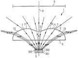
상기 광학소자(2)의 방사선 출사면(4)은 상기 광학소자의 광축(6)을 통과하는 오목하게 굽어진 부분영역(5), 및 상기 광축과의 간격을 두고 상기 오목하게 굽어진 부분영역을 에워싸는, 볼록하게 굽어진 부분영역(7)을 구비한다. 상기 볼록하고 오목한 부분영역은 특히, 볼록렌즈 또는 오목렌즈에 따라 구현될 수 있다.The
상기 광축(6)에 배치된 상기 반도체 칩(3) 위의 활성영역(303)에는, 방출된 방사선이, 바람직하게는 편평하게 형성된 방사선 출사면(8)을 지나 입사된다. 상기 반도체 칩으로부터 방출한 방사선, 특히, 가시광선은 도 1에서 화살표로 특징지 워진, 개개의 광선을 상징하는 선에 의하여 명백해진다.In the
상기 광학소자(2)는 예를 들어, 분산기(diffuser) 박막과 같은 평면(9) 또는 LCD와 같은 표시장치의 균질한 조명을 위해 형성된다. 상기 광축은 바람직하게는 도 9에 의하여 진행한다. 특히 바람직하게는, 상기 평면(9)은 상기 광축(6)에 실질적으로 수직으로 진행한다.The
상기 광학소자는 상기 평면(9)의 균질한 조명을 위해 형성된다. 상기 볼록하게 굽어진 부분영역 및 상기 오목하게 굽어진 부분영역의 적절한 곡률 형성에 의하여, 상기 반도체 칩으로부터 발생한 방사선은, 상기 평면(9)이 상기 조명장치에 의하여 균일하고 균질하게 조명되도록 방사선 출사측으로 분할될 수 있다. 상기 평면의 다양한, 균일한 크기의 영역에는 바람직하게 각각 실질적으로 동일한 방사선 성능이 직면한다.The optical element is formed for homogeneous illumination of the
상기 오목한 부분영역(5)을 지나 방출되는 방사선은 분산 렌즈에서와 유사하게 분산된다. 특히, 상기 광축과의 90도의 다양한 각도 하에서 상기 방사선 출사면 위로 발생하는 방사선이 상기 광학소자로 진입할 때 상기 광축에 의해 굴절된다.The radiation emitted past the
상기 오목한 부분영역으로부터 방출하는 방사선은 상기 광축(6)을 에워싸는 상기 평면(9)의 영역의 균질한 조명에 사용된다.The radiation emitted from the concave partial region is used for homogeneous illumination of the region of the
방위각으로 상기 광축(6) 주위로 순환하는 동일형태의, 상기 조명장치의 방사특성을 위해서, 상기 광학소자는 바람직하게는, 상기 광축(6)에 회전대칭적으로 구현된다.For the radiation characteristics of the illuminating device of the same type that circulate around the
상기 광축과 비교적 멀리 이격된 상기 평면(9)의 영역은, 상기 볼록하게 굽어진 부분영역(7)을 지나 상기 광축(6)과의 90도의 다양한 각도 하에서 상기 광학소자(2)로부터 방출되는 방사선에 의하여 조명된다. 상기 오목한 부분영역과 상기 볼록한 부분영역 사이의 전이영역은 바람직하게는 편평하게, 특히, 에지(edge)없이 형성된다. 특히, 상기 방사선 출사면, 바람직하게는, 완전평면으로, 구별할 수 있도록 형성될 수 있다. 따라서, 상기 평면(9)의 균질한 조명이 수월해진다.The area of the
상기 방사선 출사면의 볼록하게 굽어진 부분영역은 바람직하게는 상기 오목하게 굽어진 부분영역보다 큰 표면영역을 갖는다. 그 결과, 상기 오목하게 굽어진 부분영역에 비해서 증가된, 상기 방사선의 부분이 상기 볼록하게 굽어진 부분영역을 지나 상기 광학소자로부터 방출된다.The convexly curved partial region of the radiation exit surface preferably has a larger surface area than the concavely curved partial region. As a result, the portion of the radiation, which is increased compared to the concavely curved partial region, is emitted from the optical element through the convexly curved partial region.
또한, 상기 볼록하게 굽어진 부분영역은 바람직하게는, 제1 곡률의 제1 영역(81) 및 제2 곡률의 제2 영역(72)을 구비한다. 여기서, 상기 제1 곡률은 바람직하게는 상기 제2 곡률보다 작다.In addition, the convexly curved partial region preferably includes a first region 81 of a first curvature and a
상기 제2 영역(72)에서 상대적으로 큰 곡률로 인해, 상기 제2 영역에서 상기 광학소자(2)로부터 방출되는 방사선은 바람직하게는, 상기 제1 영역(71) 또는 상기 오목한 부분영역(5)에서 상기 광학소자로부터 방출되는 방사선보다 큰 각도를 갖는다. 따라서, 상기 평면(9)의 광축으로부터 비교적 멀리 이격된 영역의 균질한 조명이 수월해진다.Due to the relatively large curvature in the
바람직하게는, 상기 광학소자로부터의 광축과의 90보다 작은 각도 하에서만 방사선이 상기 광학소자로부터 방출된다. 상기 조명장치는 특히, 측면 또는 상기 광축에 대해 가로질러 앞쪽으로, 상기 광축의 방향으로 방사한다. 상기 조명장치(1)는 바람직하게는, 상기 방사선 성능의 대부분이 상기 광축에 대한 소정의 각도 하에서, 특히, 상기 볼록하게 굽어진 부분영역을 지나 상기 광학소자로부터 방출되도록 구현된다.Preferably, radiation is emitted from the optical element only under an angle less than 90 with the optical axis from the optical element. The lighting device radiates, in particular, in the direction of the optical axis, forwardly across the side or across the optical axis. The
상기 볼록한 부분영역의 곡률은 상기 오목하게 굽어진 부분영역과의 간격이 증가하면서 특히, 상기 제2 영역(72) 내에서 방사선 입사면(8)의 방향으로 증가할 수 있으므로, 상기 광축과의 큰 각도 하에서의 방사선의 증가된 분리 및 상기 광축과 비교적 멀리 이격된 상기 평면(9)의 영역의 조명이 수월해진다.The curvature of the convex partial region may increase in the direction of the
상기 조명장치(1)는, 상기 광학소자로부터 방출되는 방사선이 교차되지 않으므로, 상기 조명할 평면 위의 국부적 방사선 성능 분할은 실질적으로 상기 조명장치와의 평면의 간격과 무관하게 수행된다.The
상기 광학소자가 방사선 형성에서 방사선의 교차를 유발한다면, 초점영역이 형성될 수 있으므로, 상기 평면에서의 국부적 방사선 성능 분할은 상기 광학소자에 대한 평면의 간격과 무관할 것이다. 상기 광학소자(2)에 대한 평면(9)의 간격의 변화에서, 특히, 예를 들어, 국부적 방사선 성능분할의 높은 세기의 (링)과 같은 비균질성이 형성될 것이다. 이러한 비균질성은 방사선의 교차에 의해 유발될 것이다. 도 1에 도시된 광학소자에서, 절개없이 진행하는 방사선으로 인해, 상기 방사선 성능이 상기 광학소자(2)에 대한 평면의 간격과 무관하게 상기 평면(7)으로 국부적으로 분할된다. 또한, 상기 광학소자 내에서의 방사선 형성 또는 방사선 안내는 바람직하게는 전반사(total reflection)없이 수행된다.If the optical element causes the intersection of radiation in the formation of radiation, then a focal region may be formed, so that the local radiation performance division in the plane will be independent of the plane spacing for the optical element. In the change of the spacing of the
바람직하게는, 상기 광학소자는, 상기 반도체 칩을 포함하는 광전자부품에 고정하기 위해 구비된 개별 광학소자로 형성된다. 상기 광전자부품은, 상기 광학소자와 무관하게 고성능적용을 위해 최적화되고 이어서 상기 개별 광학소자를 구비할 수 있다. 따라서, 상기 조명장치의 개개 부품은 각각의 주요기능과 서로 무관하게 상기 광학소자의 경우에서의 방사선 형성 또는 상기 부품의 경우에서 방사선 발생이 최적화되어 제조될 수 있다.Preferably, the optical element is formed of individual optical elements provided for fixing to the optoelectronic component including the semiconductor chip. The optoelectronic component may be optimized for high performance application irrespective of the optical element and then include the individual optical element. Therefore, the individual parts of the lighting device can be produced by optimizing the radiation generation in the case of the optical element or the generation of radiation in the case of the parts irrespective of their main functions.
상기 반도체 칩(3)은 또한 바람직하게는, 박막 반도체 칩으로 형성된다. 상기 활성영역(303)을 갖는 반도체 층 시퀀스를 포함하는 상기 반도체 칩(3)의 반도체 몸체(302)는, 상기 반도체 몸체, 특히, 상기 반도체 층 시퀀스 위에서 바람직하게는 에피택셜 성장된 성장기판으로부터 분리된 캐리어(301) 위에 배치된다. 이에 따라, 상기 캐리어(301)는 성장기판에 대한 높은 요구사항을 충족시켜서는 안되며 예를 들어, 열 전도특성과 관련하여 최적화되어 구현될 수 있다. 이에 따라, 제조시 상기 성장기판이 제거되는 박막 반도체 칩은 상기 반도체 칩 안에서 발생하는 비교적 높은 손실 열을 갖는 고성능 적용에 특히 적합하다.The
도 2에는 조명장치에 특히 적합한 반도체 칩의 실시예가 개략적 단면도를 참조로 하여 도시된다.2 shows an embodiment of a semiconductor chip which is particularly suitable for a lighting device with reference to a schematic cross sectional view.
LED 칩과 같은 상기 반도체 칩(3)은, 상기 방사선발생을 위해 구비된 활성영역(303)을 갖는 반도체 층 시퀀스를 포함하는 캐리어(301)에 배치된 반도체 몸체(302)를 구비한다. 상기 캐리어로 향한, 상기 반도체 몸체의 측면 위에는 제1 콘택(304)이 배치되며, 상기 제1 콘택(304)에 의하여 상기 반도체 칩(3)이 상기 반 도체 몸체로 전향한 상기 캐리어의 측면에 배치된 제2 콘택(305)에 연결되어 전기연결가능하다. 상기 제1 콘택(304)은 특히, 본딩 와이어와의 도전적 연결을 위해 구비되고, 상기 제2 콘택(305)은 연결 도전체(이를 위해, 도 6, 7, 및 8과 관련하여 기재된 부품 참조)와의 도전적 연결을 위해 구비된다. 상기 콘택은 예를 들어, 각각 금속 또는 합금을 포함할 수 있다.The
바람직한 실시예에서, 상기 반도체 몸체(302), 특히, 상기 활성영역(303)은, 예를 들면, InxGayAll-x-yP, InxGayAl1-x-yN 또는 InxGayAl1-x-yAs(각각,0≤ x ≤1, 0≤ y ≤1, x+y≤1 )로 이루어진 물질계로부터의 적어도 하나의 III-V 반도체 물질을 포함한다.In a preferred embodiment, the
III-V 반도체 물질은 자외선(InxGayAl1-x -yN) 내에서 가시영역(InxGayAl1-x-yN, 특히, 청색 내지 녹색 방사선까지 또는 InxGayAl1-x-yP, 특히 황색 내지 적색 방사선 까지)을 지나서 적외선(InxGayAl1-x-yAS) 스펙트럼 영역에 적합하다. III-V 물질계에 의하여, 특히, 소위 물질계로부터 또한, 방사선 발생에서 바람직하게는 높은 내부 양자계수가 실현될 수 있다.III-V semiconductor material is an ultraviolet(In x Ga y Al 1 -x - y N) in the visible range(In x Ga y Al 1 -x- y N, in particular, to blue to green radiation, or Inx Gay Al1-x-y P, in particular, a yellow to red radiation up) past the infrared (inx Gay Al1-x-y AS) it is suitable for the spectral domain. By means of the III-V material system, particularly from so-called material systems and also in radiation generation, preferably high internal quantum coefficients can be realized.
또 다른 바람직한 실시예에서, 상기 활성영역(303)은 헤테로 구조, 특히, 이중 헤테로구조를 갖는다. 또한, 상기 활성영역(303)은 단일 또는 다중 양자 웰 구조를 포함할 수 있다. 이러한 구조, 특히, 다중 양자 웰 구조 또는 이중 헤테로 구조에 의하여 특히 높은 내부 양자계수가 실현될 수 있다.In another preferred embodiment, the
상기 용어 양자 웰 구조는 본 출원의 범위 내에서, 충전 캐리어가 제 한(confinement)에 의하여 에너지 상태의 양자화를 경험하는 어떠한 구조를 포함한다. 특히, 상기 용어 양자 웰 구조는 상기 양자화의 치수화에 대한 어떠한 정보를 포함하지 않는다. 따라서, 상기 양자 웰 구조는 무엇보다도, 양자 홈통(trough), 양자 와이어, 양자 점, 및 이러한 구조의 각각의 조합을 포함한다.The term quantum well structure includes any structure within the scope of the present application where the charge carriers experience quantization of the energy state by confinement. In particular, the term quantum well structure does not contain any information about the dimensioning of the quantization. Thus, the quantum well structure includes, among other things, quantum troughs, quantum wires, quantum dots, and combinations of each of these structures.
또 다른 바람직한 실시예에서, 상기 반도체 몸체(302)와 상기 캐리어(301) 사이에는 미러층(306)이 배치된다. 상기 미러층은 예를 들어, 금속함유, 특히, 실질적으로 금속의 미러층으로 구현될 수 있다. 상기 활성영역 내에서 발생한 방사선은 상기 미러층에서 반사될 수 있으므로, 상기 활성영역에서 볼 때 상기 미러층이 상기 후치된 구조, 예를 들어, 캐리어에서의 흡수가 방지될 수 있다. 상기 반도체 칩(3)의 효율이 증가될 수 있다. 예를 들어, 상기 미러층은 Au, Al, Ag, Pt, Ti 또는 이러한 물질 중의 적어도 하나를 포함하는 합금을 포함한다. Al과 Ag는 자외선 및 청색 스펙트럼 영역에서 특히 높은 반사도를 가지며, Au도 황색, 오렌지, 및 적색에서 상기 적외선 스펙트럼 영역까지 특히 높은 반사도를 갖는다. 또한, 상기 미러층에서의 반사에 의하여 상기 미러층(306)에 대향한 상기 반도체 몸체(302)에서 방출되는 방사선의 부분이 증가한다.In another preferred embodiment, a
또 다른 바람직한 실시예에서, 상기 캐리어(301)와 상기 미러층(306) 사이에는, 상기 반도체 몸체가 상기 미러층 측에서 상기 캐리어에 고정되는 연결층(307)이 배치된다. 상기 연결층(307)은 예를 들어, 납땜층으로 구현될 수 있다.In another preferred embodiment, a
도 2에 도시된 반도체 칩(3)은 박막 반도체 칩으로 구현되는데, 이는, 상기 반도체 칩의 제조시 상기 반도체 칩 위의 반도체 층 시퀀스가 예를 들어, 에피택시 에 의하여 성장된 상기 성장기판이 제거되는 것을 의미한다. 이에 따라, 상기 캐리어(301)는 특히, 상기 성장기판으로부터 분리되고, 성장기판에 대한 높은 요구사항을 충족시켜서는 안되며 상기 반도체 칩과 관련하여, 예를 들어, 높은 열 전도성과 같은 보다 바람직한 특성이 비교적 자유롭게 선택될 수 있다.The
바람직하게는, 상기 캐리어는 비교적 높은 열 전도성을 갖는다. 예를 들어, 상기 캐리어는 Ge를 포함한다. GaAS 캐리어도 적용할 수 있다.Preferably, the carrier has a relatively high thermal conductivity. For example, the carrier comprises Ge. GaAS carriers can also be applied.
상기 활성영역(303)은 바람직하게는, 도전성 캐리어, 도전성 연결층, 전기도전성 미러층, 및 상기 반도체 층 시퀀스에 의하여 상기 제2 콘택(305)에 연결된다.The
상기 캐리어가 반도체 물질을 포함하는 경우, 상기 캐리어는 바람직하게는 도전성 향상에 적합하게 도핑된다.If the carrier comprises a semiconductor material, the carrier is preferably doped to improve conductivity.
박막 반도체 칩을 제조하기 위해서, 예를 들어, 우선적으로, 상기 반도체 몸체(302)의 상기 반도체 층 시퀀스는 상기 성장기판 위에서 제조된다. 이어서, 상기 성장기판으로 전향한, 상기 반도체 층 시퀀스의 측면 위에는 미러 층이 증발에 의하여, 특히, 스퍼터링에 의하여 배치된다. 상기 미러 층 측에는, 반도체 층 시퀀스과 성장기판과의 결합물이 상기 연결층(307)을 지나 상기 캐리어(301)에 연결되므로, 상기 성장기판은 식각 또는 레이저 분리에 의하여 이격되거나 제거된다.In order to fabricate a thin film semiconductor chip, for example, first of all, the semiconductor layer sequence of the
박막 반도체 칩은 특히, 미러 층을 사용함으로써, 바람직하게는 고효율성에 의하여 특징지워진다. 또한, 박막 반도체 칩은 실질적으로 람베르트(Lambert)식 방사기에 상응하는 코사인(cosine) 형태의 방사특성을 가질 수 있다. 박막 반도체 칩, 특히, 금속함유 미러 층에 의하여, 표면방사기로 구현된 반도체 칩이 간소화되 어 실현될 수 있다.Thin film semiconductor chips are particularly characterized by the use of mirror layers, preferably by high efficiency. In addition, the thin film semiconductor chip may have a cosine-like radiation characteristic substantially corresponding to a Lambert radiator. By the thin film semiconductor chip, in particular, the metal-containing mirror layer, the semiconductor chip implemented by the surface radiator can be simplified and realized.
박막 발광다이오드 칩과 같은 박막 반도체 칩은 또한, 하기와 같은 특징에 의하여 특징지울 수 있다.Thin film semiconductor chips such as thin film light emitting diode chips can also be characterized by the following features.
- 예를 들어, 캐리어(301)과 같은 캐리어 부재 쪽으로 향한, 활성영역을 포함하는 반도체 층 시퀀스, 특히, 에피택시 층 시퀀스의 제1 주요면에는 미러 층이 배치되거나, 상기 반도체 층 시퀀스 내에서 발생한 방사선의 적어도 일부는 그 안으로 재반사되는 상기 반도체 층 시퀀스 안에 통합되어 브래그 미러로 형성되거나,A mirror layer is arranged on the first major surface of the semiconductor layer sequence comprising the active region, in particular towards the carrier member, for example the
- 상기 반도체 층 시퀀스는 20㎛ 이하 영역의 두께, 특히, 10㎛의 영역 내의 두께를 가지며,The semiconductor layer sequence has a thickness in the region of 20 μm or less, in particular in the region of 10 μm,
- 상기 반도체 층 시퀀스는, 이상적인 경우 빛을 상기 반도체 층 시퀀스 내에서 거의 에르고딕 분할(ergodic distribution)을 유발하는 혼합구조물을 구비하는 적어도 하나의 평면을 갖는 적어도 하나의 반도체 층을 포함하는데, 즉, 상기 반도체 층 시퀀스는 가능한한 에르고딕 추측통계학상의 분산행태를 갖는다.The semiconductor layer sequence comprises at least one semiconductor layer having at least one plane with a mixed structure which ideally causes light to ergodic distribution almost within the semiconductor layer sequence, ie The semiconductor layer sequence has as much ergodic speculative statistics as possible.
박막 발광다이오드 칩의 기본원칙은 예를 들어, 아이 슈니처(I. Schnitzer et al.), Appl. Phys. Lett. 63(16), 1993년 10월 18일, 2174-2176에 기재되어 있으며, 그 개시내용은 본원으로의 재귀적 방법에 의하여 생략된다.Basic principles of thin film light emitting diode chips are described, for example, in I. Schnitzer et al., Appl. Phys. Lett. 63 (16), October 18, 1993, 2174-2176, the disclosure of which is omitted by a recursive method herein.
상기 조명장치가 자명하게도 박막 반도체 칩만으로만 실현될 수 없다는 것을 알 수 있다. 상기 성장기판이 제거되지 않는 반도체 칩과 같은 또 다른 반도체 칩도 조명장치에 적합할 수 있다. 고효율성과 간소하게 실현가능한, 바람직하게는, 직접 상기 광학소자의 방향을 향하여 증가된 표면방출로 인해, 박막 반도체 칩이 특히 적합하다.Obviously, it can be seen that the lighting device cannot be realized only by the thin film semiconductor chip. Another semiconductor chip, such as a semiconductor chip from which the growth substrate is not removed, may also be suitable for lighting devices. Thin film semiconductor chips are particularly suitable due to their high efficiency and simply feasible, preferably due to the increased surface emission directly towards the optical element.
도 3에는, 본 발명에 따른 조명장치의 방사특성의 예가 도시되어 있다. 상대적 세기를 상기 광축과의 각도(
여기에 도시된 방사특성은 상기 광축에 대해 회전대칭적으로 구현된 도 1의 광학소자(2)를 위해서, 그리고, 상기 방사선 입사면(8)과의 0.6mm 간격을 두고 배치된 도 2의 반도체 칩(3)을 위해서 검출되었다.The radiation characteristics shown here are for the
상기 조명장치는 바람직하게는, 상기 광축에 대해 측면으로, 특히, 비교적 큰 각도 하에서, 반사선 성능의 대부분을 검출한다. 바람직하게는, 상기 광축을 에워싸는, 오목하게 굽어진 부분영역을 분리하는 방사선 성능은 특히, 0°과 10°사이의 각도 영역 내의 특성의 국부적 최소값을 갖는다.The illumination device preferably detects most of the reflection line performance laterally with respect to the optical axis, in particular under relatively large angles. Preferably, the radiation performance of separating the concavely curved subregions surrounding the optical axis, in particular, has a local minimum of properties in the angular region between 0 ° and 10 °.
또한, 상기 조명장치는 상기 광축에 대한 80°과 40°사이의 각도 영역에서 상기 반도체 칩으로부터 발생한 방사선 성능의, 바람직하게는, 50% 이상, 특히 바람직하게는, 60% 이상을 검출한다.Further, the illumination device detects, preferably, at least 50%, particularly preferably at least 60% of the radiation performance generated from the semiconductor chip in an angular region between 80 ° and 40 ° with respect to the optical axis.
상기 세기의 최대값은 대략 70°이다. 대략 0°로 영역에 대응하는 상기 오목한 부분영역(5)으로부터 시작하여, 상기 세기는 각도가 증가하면서 성장하는데, 이는, 대략 잠재력 기능에 따라, 특히, 포물선에 따라 상기 볼록하게 굽어진 부분영역에 상응하며, 상기 최대값에 도달한 후에 가파르게 하강한다.The maximum value of the intensity is approximately 70 °. Starting from the
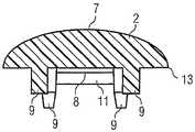
도 4는 도 4A 내지 도 4F에서 본 발명에 따른 조명장치에 특히 적합한 광학소자(2)의 다양한 개략적 측면도를 도시한다. 여기서, 도 4A는 상기 광학소자의 방사선 입사면(8)의 하부로부터 본 경사도를 도시하고, 도 4B는 상기 광학소자의 방사선 출사면(4)의 상부로부터 본 경사도를 도시하고, 도 4C는 상기 방사선 입사면의 도면이며, 도 4D는 측면도이고, 도 4E는 도 4C의 E-E 선에 따른 단면도이고, 도 4F는 도 4C의 F-F 선에 따른 단면도이다.4 shows various schematic side views of an
실질적으로, 상기 광학소자는 도 1에 도시된 광학소자에 해당한다. 실질적으로 상기 광학소자(2)의 광학 기능영역이 도시된 도 1의 광학소자와의 차이점은, 도 4에 도시된 실시예에 따른 광학소자(2)는 다수의 고정부재(9) 및 안내부재(10)를 구비한다는 점이다.Substantially, the optical element corresponds to the optical element shown in FIG. Substantially different from the optical element of FIG. 1 in which the optical functional region of the
또한, 상기 광학소자(2)는 적어도 하나의 배향부재(11), 바람직하게는 다수의 배향부재를 포함한다.In addition, the
상기 광학소자(2)는 특히, 상기 조명장치의 하우징 몸체 및 상기 반도체 칩을 구비하는 개별 광전자부품에 고정하기 위해서 형성된다(이에 대해 도 6, 도 7, 및 도 8 참조).The
상기 광학소자(2)는 방사선투과적으로 구현되며, 예를 들어, 방사선투과 실리콘 또는 실리콘 경화재를 포함한다.The
상기 광학소자(2)는 경우에 따라서는, 예를 들어, 아크릴 경화재 또는 에폭시 경화재와 같은 반응 경화재를 포함하거나 실리콘 없이 구현될 수 있다. 경우에 따라서는, 상기 광학소자는 열가소성 물질을 포함하거나 열가소성 물질로 이루어질 수 있다.In some cases, the
상기 광학소자는 바람직하게는, 다이 캐스팅(die casting), 다이 압착 캐스 팅(die press casting) 또는 압착 캐스팅에 의하여 제조된다. 이러한 방법을 사용하여, 상기 고정부재(9), 상기 안내부재(10) 및/또는 상기 배향부재(11)도 제조될 수 있다. 특히, 상기 언급한 부재들과 상기 광학소자는 일체로 형성될 수 있다. 바람직하게는, 상기 광학부재는 후면 절개가 없다. 캐스팅 도구 내에 비용이 많이 드는 슬라이더(slider)의 사용이 필요하지 않을 수 있다. 상기 광학소자를 상기 캐스팅 도구로부터 수월하게 제거하기 위해서, 고정부재(9), 상기 안내부재(10) 및/또는 상기 배향부재(11)는 경사지게 구현될 수 있고 따라서 소위 제거 경사를 가질 수 있다.The optical element is preferably manufactured by die casting, die press casting or compression casting. Using this method, the fixing
상기 고정부재(9), 상기 안내부재(10) 및/또는 상기 배향부재(11)는 바람직하게는, 상기 광학소자의 방사선 입사면 측에 배치된다.The fixing
상기 안내부재(10)는, 바람직하게는, 상기 광학소자(2)를 상기 광전자부품에 고정할 때 상기 고정부재가, 상기 광전자부품의 상응하는 고정장치에 대해서 쉽게 조정된 상기 고정부재의 배치에서 상기 광전자부품의 상응하는 고정장치로 슬라이딩되거나, 안내되거나 상기 고정부재는 상기 고정장치에 공급되도록 형성된다. 이를 위해, 상기 안내부재(10)는 상기 방사선 입사면으로 전향한 측면에 경사져 구현된다. 상기 안내부재는 이를 위해 경사부(12)를 구비한다. 상기 안내부재(10)는 바람직하게는, 상기 방사선 입사면(8)과의 간격이 증가하면서 상기 경사진 영역 내에서 축소된다. 바람직하게는, 상기 안내부재(10)는 일체로, 특히, 상기 방사선 입사면측에서 상기 광학소자(2)에 인접하는 전향된 측면 위에서 경사진다.The
상기 고정부재(9)는 도 4의 실시예에서 개개의 핀(pin)으로 구현된다. 예를 들어, 상기 고정부재는 압착 캐스팅을 위해 구현되며, 바람직하게는, 연속적으로, 상기 방사선 입사면(8)과의 간격이 증가하면서 축소된다. 상기 고정부재(9)의 직경은 이에 따라, 상기 방사선 입사면(8)과의 간격이 증가하면서 축소될 수 있다.The fixing
상기 방사선 입사면(8) 측에는 상기 광학소자(2)가 상기 에지(13)에 의하여 제한된다. 상기 안내부재(10)는 상기 고정부재(9)에 비해서 상기 에지(13)에 더 가까이 배치된다. 상기 광학소자를 상기 광전자부품에 고정하는 것이 바람직하게는 수월해지며, 조명장치의 전체안정성이 상기 광전자부품과 거기에 고정된 광학소자에 의하여 향상된다.On the
고정부재에, 바람직하게는, 다수의 안내부재, 대략 두 개의 안내부재가 할당 됨으로써, 상기 광학소자를 상기 광전자부품에 고정하는 것이 상기 광학소자의 실장시 개선된 안내로 인해 바람직하게는 계속적으로 수월해진다. 고정부재에 할당된 안내부재는 상기 고정부재에, 바람직하게는 직접 인접하게 배치된다.Preferably, a plurality of guide members, approximately two guide members, are assigned to the fixing member, so that the fixing of the optical element to the optoelectronic component is preferably continually facilitated due to improved guidance in mounting the optical element. Lose. The guide member assigned to the stationary member is preferably arranged directly adjacent to the stationary member.
상기 배향부재(11)는 바람직하게는, 상기 광학소자를 상기 광전자부품에 설치하는 것, 특히, 상기 광학소자를 상기 부품에 배향적으로 배치하는 것을 수월케 한다. 상기 부품에 고정하기 위한 광학소자가 삽입될 수 있는 실장도구에는 상기 배향부재에 상응하는 배향장치가 구비될 수 있다. 상기 배향장치에는 상기 배향부재, 특히, 상기 광학소자를 상기 도구 내에 기계적으로 안정되고 분리가능하게 고정하기 위한 배향부재가 개재될 수 있다. 따라서, 실장을 위해 상기 광학소자를 설치장비의 상기 실장도구 내에 소정 배향하는 것이 보장될 수 있다. 바람직하게는, 상기 배향부재는 상기 에지(13) 위로 돌출하므로, 특히, 상기 도구의 시작점이 형성되고 상기 실장이 간단해진다.The
또한, 상기 광학소자는 상기 방사선 입사면(8) 위에서 볼 때 바람직하게는, 실질적으로 원형으로 형성된다. 또한, 상기 광학소자는 상기 방사선 입사면(8) 위에서 볼 때 바람직하게는, 도 4C의 대칭 축(E-E) 및/또는 (D-D)에 대해 축대칭적으로 형성되거나, 상기 방사선 입사면의 중앙점에 대해 점대칭적으로 형성된다.In addition, the optical element is preferably formed substantially circularly when viewed from the
도 5는 본 발명에 따른 조명장치의 광학소자(2)의 또 다른 실시예를 이러한 광학소자의 방사선 입사면(8) 위의 개략적 도면을 참조로 하여 도시한다.Figure 5 shows another embodiment of an
도 5에 도시된 광학소자(2)는 실질적으로 도 4에 도시된 광학소자에 해당한다. 도 4와의 차이점은, 도 5의 광학소자에서 개별 배향부재가 필요하지 않다는 점이다. 오히려, 상기 안내부재(10)가 부분적으로 배향부재(11)로도 형성된다. 바람직하게는, 개별 배향부재(11)의 형성이 필요하지 않을 수 있다. 배향부재로 형성된 안내부재(11)는 바람직하게는, 상기 에지(13) 위로 돌출한다.The
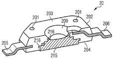
도 6에는, 본 발명에 따른, 광전자부품에 고정된 광학소자를 구비한 조명장치의 제2 실시예의 개략적 도면을 나타낸다.Fig. 6 shows a schematic view of a second embodiment of a lighting device with an optical element fixed to an optoelectronic component according to the invention.
상기 조명장치(1)는 상기 반도체 칩(3)을 구비하는 광전자부품(20)을 포함한다. 상기 광학소자(2), 예를 들어, 전술한 도면에 따라 형성된 상기 광학소자(2)는 상기 고정부재(9)를 사용하여 상기 광전자부품(20)에 고정된다.The
상기 광학소자를 고정하기 위해서, 상기 광전자부품(1) 안에는 고정장치(201)가 형성되며, 상기 고정장치(201) 안으로 상기 고정부재(9)가 고정시 개재된다. 상기 고정장치(201)는 바람직하게는, 리세스로 형성되며, 상기 리세스는 상 기 광전자부품의 하우징 몸체(203)의 제1 주요 면(202)로부터 상기 제1 주요 면(202)에 대향하는, 상기 하우징 몸체의 제2 주요 면(204)까지 이른다. 상기 리세스는 상기 하우징 몸체를 특히 완전히 관통한다. 상기 고정장치는 예를 들어, 상기 하우징 몸체를 제조할 때 이미 상기 하우징 몸체 안에 예비제조될 수 있다. 예를 들어, 상기 고정장치는 실린더 형태로 구현된다. 상기 고정장치는 경우에 따라서는, 상기 하우징 몸체를 완전히 관통하지않는 제거부로도 형성될 수 있다.In order to fix the optical element, a fixing
상기 고정부재(9)는 압축 끼워맞춤(press fit)을 사용하여 고정을 위해 구현된다. 이를 위해, 상기 고정부재(9)는 바람직하게는, 상기 광학소자(2)의 방사선 입사면(8)과의 간격이 증가하면서 축소된다. 상기 광학소자(2)는 상기 광전자부품 위에 배치되며, 여기서, 상기 고정부재(9)는 상기 고정장치(201) 안으로 개재된다. 상기 고정부재가 상기 하우징 몸체와 접촉하여 상기 고정부재로 압력이 가해지면, 상기 광학소자가 상기 고정장치로 보다 멀리 안으로 압축하는 동작이, 상기 광학소자가 최종적으로 압축 끼워맞춤을 사용하여 기계적으로 안정적으로 상기 하우징 몸체(203)에 고정되도록 향상된다.The fixing
상기 광전자부품(20)에 고정된 광학소자(2)의 방사선 입사면(8)은 바람직하게는, 상기 광전자부품과 이격되고, 특히 바람직하게는, 상기 하우징 몸체, 특히, 그의 제1 주요 면(202)과 이격된다. 이를 위해, 상기 고정부재(9)는 바람직하게는, 상기 방사선 입사면(8)에 인접한 영역에서 상기 고정장치의 측면 신장에 비해상대적으로 큰 측면 신장을 특히 상기 제1 주요 면과 평행하게 구비한다.The
상기 광학소자, 특히, 그의 방사선 입사면(8)에 대한 반도체 칩의 간격은 1mm 이하일 수 있다. 0.6mm의 간격은 특히 바람직하게 제조되었다.The spacing of the semiconductor chip with respect to the optical element, in particular its
상기 광학소자를 상기 광전자부품에 고정하기 위해서 압축 끼워맞춤만이 적합하지 않다는 것을 알 수 있다. 상술한 방법들, 열간 압축, 리프팅, 열간 리프팅, 열적 리벳팅 또는 접착도 경우에 따라서는 상기 고정부재 및/또는 상기 고정장치의 적합한 변형 하에서 적용될 수 있다.It can be seen that only the compression fit is not suitable for fixing the optical element to the optoelectronic component. The aforementioned methods, hot compression, lifting, hot lifting, thermal riveting or adhesion, may also be applied under appropriate modifications of the fixing member and / or the fixing device, as the case may be.
열적 리벳팅(thermal riveting)을 위해서, 예를 들어, 상기 고정부재는 상기 하우징 몸체(203)의 제2 주요 면(204) 측에서 상기 고정장치로 안내한 후에 상기 제2 주요 면 위로 돌출한다. 상기 돌출하는 고정부재(9)의 부분 편(partial piece)에서, 상기 고정부재는 이어서, 적어도 이러한 부분영역에서 유동적이 되도록 가열된다. 상기 유동적인 부분 편은 상기 고정장치 및/또는 상기 하우징 몸체에 형성된다("흐른다"). 따라서, 상기 고정부재를 냉각하고 경화한 후에 상기 광학소자(2)를 상기 광전자부품(20)에 기계적으로 안정적이게 고정한다. 경우에 따라서는, 상기 하우징 몸체도 상기 제2 주요 면 측에서 상기 고정부재에 인접하는 영역 내에서 가열되므로, 상기 하우징 몸체와 상기 유동적인 고정부재가 용해된다.For thermal riveting, for example, the fastening member protrudes above the second major face after guiding it to the fixture on the second
상기 고정장치(201)의 측면 신장은 상기 제2 주요 면측에서의 열적 리벳팅을 위해서 바람직하게는, 상기 고정부재(9)보다 더 크며, 특히 바람직하게는, 상기 제1 주요 면(202)의 방향으로 축소된다. 상기 고정부재를 상기 고정장치에 안내한 후에, 상기 고정부재에 의해 채워지지 않은 상기 고정장치의 자유 체적은, 상기 고정부재를 가열하기 전에 상기 제2 주요 면으로 돌출하는 물질을 수용하기 위해 결정된다. 이를 위해, 상기 고정장치는 바람직하게는, 상기 하우징 몸체의 제2 주요 면에 인접한 영역 내에서 상기 제1 주요 면의 방향으로 축소되는, 대략 사다리꼴 형태의 횡단면으로 형성된다. 이러한 축소 후에 상기 고정장치는 실질적으로 실린더 형태로 상기 제1 주요 면의 방향으로 신장될 수 있다.Lateral elongation of the fixing
상기 광학소자(2)는 또한, 상기 측면(217) 위로 측방향으로 상기 하우징 몸체로 돌출할 수 있다. 상기 돌출하는 영역 내에서, 이러한 영역 내에서 광학기능이 속하지 않는 상기 방사선 입사면(8)에 안내부재 및/또는 배향부재가 배치될 수 있다(도 4에 도시된 광학소자의 실시예 참조).The
상기 광전자부품(20)은 제1 전기연결도체(205) 및 제2 전기연결도체(206)를 포함한다. 이러한 광전자부품(20)은 바람직하게는, 상기 하우징 몸체의 다양한 측면에서 상기 하우징 몸체로 돌출한다. 상기 연결도체는 상기 반도체 칩(3)의 전기접촉에 사용된다. 상기 반도체 칩(3)은 도전 접착제 또는 솔더링 층과 같은 연결층(207)에 의하여 상기 제1 연결도체(205)와 도전적으로 연결되거나 이에 고정될 수 있다. 상기 제2 연결도체(206)에 의하여, 상기 반도체 칩은 바람직하게는 본딩 와이어(208)에 의하여 도전연결된다.The
상기 광전자부품(20), 특히, 상기 하우징 몸체는, 상기 두 개의 연결도체(205, 206)를 포함하는, 적합한 몰딩 배치(moulding batch)를 구비한 리드 프레임의 다이 캐스팅, 다이 압축 캐스팅 또는 압축 캐스팅 방법과 같은 리캐스팅(recasting)에 의하거나, 플라스틱 물질, 특히, 에폭시 또는 아크릴계 물질, 반응 경화재를 사용하여 제조될 수 있다. 이어서, 상기 반도체 칩(3)은 상기 연결도체에 연결될 수 있다. 따라서, 상기 광전자부품은 예비형성된 하우징, 특히, 소위 예비몰딩 패키지(premoulded package)를 구비한다.The
바람직하게는, 상기 하우징 몸체(203)는 상기 반도체 칩(3)이 배치된 캐비티 cavity)(209)를 구비한다. 또한, 상기 캐비티(209) 안에는, 상기 반도체 칩(3)이 삽입된 코팅부(210)가 배치될 수 있다. 이러한 코팅부는 상기 반도체 칩(3)과 상기 본딩 와이어(208)를, 바람직하게는 해로운 외부영향으로부터 보호한다. 예를 들어, 상기 코팅부는 아크릴 경화재 또는 에폭시 경화재와 같은 반응 경화재, 실리콘 경화재 또는 실리콘을 포함한다. 상기 코팅부는 보호가 더 잘 되도록 바람직하게는 단단하다.Preferably, the
상기 광전자부품은 또한, 혼색, 특히, 백색광을 발생하기 위해 형성될 수 있다. 이를 위해, 상기 반도체 칩으로부터 발생한 방사선의 일부는 예를 들어, 상기 코팅부(210) 안에 배치된 루미네선스 전환물질, 예를 들어, 발광물질, 특히, 입자 형태의 발광물질을 상대적으로 긴 회전축의 방사선을 방출하기 위해 여기(excite)한다. 상기 반도체 칩으로부터 발생하고 상기 루미네선스 전환물질로부터 재방출된 방사선의 혼합으로부터, 결과적으로 혼색, 특히, 백색광이 발생한다. 백색광을 발생하는 데에는 상기 반도체 칩으로부터 발생한, 청색 스펙트럼 영역 내의 일차 방사선과, 상기 루미네선스 전환물질로부터 재방출된 황색 스펙트럼 영역 내의 방사선이 특히 적합하다.The optoelectronic component can also be formed to generate mixed colors, in particular white light. To this end, a portion of the radiation generated from the semiconductor chip, for example, a luminescence conversion material, for example, a light emitting material, in particular, a light emitting material in the form of particles, a relatively long rotation axis disposed in the
상기 하우징 몸체(203)는 바람직하게는, 양호하게 반사하는 물질, 예를 들어, 백색 플라스틱으로 제조된다. 상기 캐비키의 벽은 상기 반도체 칩으로부터 발생한 방사선의 반사를 더 증가시키기 위해 상기 캐비티의 벽에서 금속과 같은 반사 증가물질로 코팅될 수 있다. 상기 캐비티의 벽에서의 반사에 의하여, 방사선형성을 위해 상기 광학소자(2)에 공급된 방사선의 부분은 캐비티(209)를 구비하지 않는 하우징 몸체에 비해서 증가될 수 있다.The
상기 광전자부품은 또한 바람직하게는, 표면실장가능하게(SMD: Surface Mountable Device) 형성된다. 상기 표면실장시 예를 들어, 상기 연결도체(205, 206)는 상기 연결도체의 납땜면(211, 212)측에서 인쇄회로기판(PCB)(도시되지 않음)의 도전체 경로 위에서 납땜된다.The optoelectronic component is also preferably formed of a surface mountable device (SMD). In the surface mounting, for example, the connecting
상기 광학소자(2)가 상기 광전자부품을 실장하기 전에 상기 광전자부품에 고정되는 경우, 상기 전체 조명장치(1)는 상기 광전자부품(20)과 이에 고정된 광학소자(2)에 의하여 표면실장가능하게 구현된다.When the
상기 광학소자(2)와 상기 반도체 칩(3) 사이에는 중간층(14)이 배치된다. 상기 중간층은 상기 코팅부(210)에 인접하고 방사선 입사측에서 상기 광학소자에 인접한다. 상기 중간층(14)은 또한 소성 성형가능하게 구현될 있다.An
바람직하게는, 상기 중간층의 물질은 접착제로 형성되므로, 상기 광학소자를 상기 광전자부품에 기계적으로 연결하는 것이 향상된다.Preferably, the material of the intermediate layer is formed of an adhesive, thereby improving the mechanical coupling of the optical element to the optoelectronic component.
또한, 상기 중간층은 바람직하게는, 굴절률 적응층으로 구현된다. 상기 굴절률 적응층은, 상기 반도체 칩(3)으로부터 발생한 방사선이 상기 광학소자와 결합되기 전에 경험하는 굴절률 도약을 결여된 중간층에 대해서 방지한다. 예를 들어, 상기 광학소자는, 상기 중간층에 대한 코팅부의 굴절률 또는 상기 광학소자에 대한 중간층의 굴절률과 같은 상기 굴절률을 서로 제한하는 물질이 1.4:1.6 이하로 유지 되도록 상기 중간층과 상기 코팅부를 서로 조정할 수 있다. 따라서, 경계면에서의 반사손실이 방지된다.In addition, the intermediate layer is preferably implemented with a refractive index adaptation layer. The refractive index adaptation layer prevents the intermediate layer lacking the refractive index leap experienced before the radiation generated from the
바람직하게는, 상기 코팅부, 상기 중간층, 및 상기 광학소자는 실리콘을 포함한다. 따라서, 굴절률 적응이 간단하게 수행될 수 있다.Preferably, the coating part, the intermediate layer, and the optical element comprises silicon. Therefore, refractive index adaptation can be performed simply.
상기 코팅부 및 상기 광학소자는 상기 중간층에 비해서 바람직하게는 단단한데, 즉, 현저히 높은 힘 소모 하에서만 소성 성형가능하게 구현된다.The coating and the optical element are preferably harder than the intermediate layer, i.e., they are plastically moldable only under a significantly high power consumption.
독일 회사 박커 케미(Wacker Chemie)사의 SilGel 612와 같은 실리콘 겔을 특히, 대략 1:1(이를 위해 상응하는 데이터시트 참조)의 두 개의 부품의 혼합비로 포함하는 중간층이 특히 적합하다. 실리콘 겔로서 SilGel 612는 동시에 접착 효과를 가질 수 있고 소성 성형가능하며 굴절률 도약을 줄일 수 있다. 이는, 특히, 상기 코팅부 및/또는 상기 광학소자가 실리콘을 포함하는 경우에 적용된다.Particularly suitable are interlayers comprising a silicone gel such as SilGel 612 from the German company Wacker Chemie in a mixing ratio of two parts of approximately 1: 1 (see corresponding datasheet for this). As a silicone gel, SilGel 612 can have an adhesive effect at the same time, be plastic moldable and reduce the refractive index jump. This applies in particular when the coating and / or the optical element comprises silicon.
상기 중간층은 상기 코팅부(210)와, 방사선 결합을 위해 사용된 상기 방사선 입사면(8)의 광학적 영역을 바람직하게는 완전히 덮음으로써, 경계면에서의 반사손실이 바람직하게는 적게 유지된다.The intermediate layer preferably completely covers the
가열시, 상기 중간층은 상기 광학소자와 상기 하우징 몸체(203)의 제1 주요 면(202) 사이에 형성된 중간공간(15)으로 신장될 수 있으므로, 상기 조명장치(1)의 기계적 부하, 특히, 상기 코팅부(210)과 상기 광학소자의 기계적 부하가 온도변동에서 바람직하게는 작게 유지된다.Upon heating, the intermediate layer can extend into an
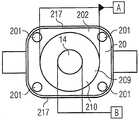
도 7에는, 조명장치에 특히 적합한 광전자부품이 도 7A의 광전자부품의 개략적 사시도와 도 7B의 부품의 개략적 사시단면도를 참조로 하여 도시되어 있다.In Fig. 7, an optoelectronic component particularly suitable for the lighting device is shown with reference to a schematic perspective view of the optoelectronic component of Fig. 7A and a schematic perspective cross-sectional view of the component of Fig. 7B.
이러한 광전자부품은 예를 들어, WO 02/084749에 보다 상세히 기재되어 있으며 그 개시내용은 본원에 대한 참조에 의하여 명백히 생략한다. 광전자부품으로 유형표시 LW W5SG(제조자: 오스람 옵토 세미컨덕터 GmbH)와 유사한 부품, 이에 변형되거나 유사한, 동일 제조자의 부품이 특히 적합하다.Such optoelectronic components are described in more detail, for example, in WO 02/084749, the disclosure of which is expressly omitted by reference to the present application. Particularly suitable for optoelectronic components are parts similar to the type designation LW W5SG (manufacturer: Osram Opto Semiconductor GmbH), variants of which are similar or similar.
상기 광전자부품(20)은 제1 전기연결도체(205) 및 제2 전기연결도체(206)를 포함하며, 이들은 상기 광전자부품(20)의 하우징 몸체(203)의 다양한 측면으로부터 돌출할 수 있고 예를 들어, 발진(oscillation) 형태로 형성될 수 있다.The
상기 하우징 몸체(203)는 코팅부(210)가 삽입된 상기 반도체 칩(3)이 배치된 캐비티(209)를 구비한다. 상기 반도체 칩(3)은 상기 연결도체(205)에 예를 들어, 솔더링 연결에 의하여 도전적으로 연결된다. 제2 연결도체(206)과의 도전적 연결은 상기 본딩 와이어(208)에 의하여 제조된다. 상기 본딩 와이어를 상기 제2 연결도체(206)에 연결하는 것이 바람직하게는, 상기 캐비티(209)의 벽(214)의 돌출부 (213)의 영역 내에서 수행된다.The
상기 반도체 칩(3)은 칩 캐리어로 기능하는 열적 연결부(215) 위에 배치된다. 상기 열적 연결부는 수직방향으로 바람직하게는, 상기 캐비티로부터 상기 하우징 몸체(203)의 제2 주요 면(204)까지 신장되며, 특히, 상기 열적 연결부 위의 칩 실장면에 대해서, 상기 제2 주요 면측에서 상기 반도체 칩(3)을 외부의 열전도장치, 예를 들어, 구리로 이루어진 냉각체에 연결하는 대면적, 열적 연결을 수월케 한다. 상기 하우징 몸체의 열적 부하는, 특히,고성능 반도체 칩을 구비한 고성능 부품(도 2에 기재된 반도체 칩과의 관계 참조)으로의 부품 동작시 바람직하게는 감 소될 수 있다. 상기 광전자부품은 고방사선 성능을 발생하기 위해, 열적 연결부로 인해 동시에 바람직하게는 개선된 열 방출시 형성될 수 있다. 이러한 광전자부품은 평면을 조명하기 위해, 즉, LCD와 같은 표시장치의 후면조명에 특히 적합하다.The
상기 열적 연결부는 예를 들어, 상기 제1 연결도체(205)의 브래킷(bracket) 안에 삽입되거나 다른 측면으로는 상기 제1 연결도체에, 특히, 도전적이거나 기계적으로 측면으로 포괄적으로 연결된다. 상기 본딩 와이어(208)와의 접촉을 위해 구비된 상기 제2 연결도체(206)는 바람직하게는, 상기 반도체 칩(3)을 상기 열적 연결부(215) 위로의 칩 실장면과 관련해서 향상된다. 방사선의 반사를 위해 사용되는 상기 캐비티의 벽의 평면은 바람직하게는 크게 유지된다. 또한, 사기 열적 연결부 자체는 반사적으로 구현될 수 있고, 그리고 나서, 바람직하게는 상기 캐비티의 바닥 및/또는 벽의 일부를 형성한다. 상기 열적 연결부는 또한, 상기 제2 주요 면 측에서 상기 하우징 몸체로부터 돌출하거나 실질적으로 상기 하우징 몸체와 편평하게 폐쇄된다. 예를 들어, 상기 열적 연결부는 예를 들어, 구리 또는 알루미늄와 같은 높은 열전도성을 갖는 금속 또는 CuW 합금과 같은 합금을 포함한다.The thermal connection, for example, is inserted into a bracket of the
상기 두 개의 연결도체(205, 206)와 상기 열적 연결부(215)를 구비한 리드 프레임은 이러한 광전자부품을 제조할 때, 다이 캐스팅과 같은 적합한 캐스팅 방법으로 상기 하우징 몸체의 금속에 의해 변형될 수 있다. 상기 반도체 칩은 상기 하우징 몸체의 제조 후에 상기 예비몰딩-하우징 부근 또는 그 안에 배치된다. 상기 열적 연결부(215)는 바람직하게는, 하나 또는 다수의 돌출부 또는 곡률부(216)에 의하여 형성되므로, 상기 열적 연결부를 상기 하우징 몸체에 기계적으로 연결하는 것이 개선되고 상기 광전자부품의 전체 안정성이 향상된다.The lead frame having the two connecting
상기 하우징 몸체의 제1 주요 면(202) 측에, 상기 광학소자를 고정하기 위해 구비된 고정장치(201)가 형성된다. 이때, 상기 광학소자는 예를 들어, 상술한 실시예에 상응하게 구현될 수 있다. 상기 광학소자를 상기 하우징 몸체(203)에 고정하기 위해, 예를 들어, 4개의 고정장치(201)가 구비될 수 있으며, 상기 고정장치(201)는 상기 광학소자를 상기 부품에 기계적으로 안정적으로 고정하는 것을 수월케 한다. 바람직하게는, 상기 고정장치(201)는 상기 하우징 몸체(203)의 제1 주요 면(202)의 모서리 영역에 배치된다.On the side of the first
도 8은 도 8A 내지 도 8D에서 본 발명에 따른 조명장치의 광전자부품 및 실시예의 다양한 개략적 도면을 나타낸다. 도 8A는 상기 광전자부품의 측면도이고, 도 8B는 상기 광전자부품(20)의 도면이며, 도 8C는 상부에서 본 상기 광전자부품의 경사도이며, 도 8D는 상기 광전자부품에 고정된 광학소자(2)를 구비한 상기 조명장치(1)의 측면도이다. 도 8에 도시된 광전자부품(20)은 예를 들어, 도 7에 기재된 부품에 따라 구현된다.8 shows various schematic views of optoelectronic components and embodiments of the lighting apparatus according to the invention in FIGS. 8A-8D. 8A is a side view of the optoelectronic component, FIG. 8B is a view of the
도 8과의 차이점은, 바람직하게는 상기 반도체 칩과 상기 본딩 와이어(208)를 단단히 보호하는 물질을 포함하는 상기 캐비티(209)에 배치된 코팅부(210) 위에는 상기 중간층(14)의 물질이 액적(droplets) 또는 반구(hemisphere) 형태로 배치된다는 점이다. 상기 중간층의 물질의 직경(B)은 바람직하게는 상기 캐비티(209)의 직경(A)보다 작다. 상기 중간층(14)의 물질은 여기서 바람직하게는 소성 성형가능하게 형성된다. 예를 들어, 상기 물질은 상술한 유형과 같은 실리콘 겔을 포 함한다. 상기 중간층의 물질은 액상으로 상기 광전자부품 위, 특히, 상기 코팅부(210) 위에 배치되거나 떨어질 수 있다. 바람직하게는, 상기 물질은 이어서 단단하지만 소성 성형가능한 상(phase)으로 이전된다. 이를 위해, 상기 광전자부품이 예를 들어, 140도의 온도로 가열될 수 있고, 상기 중간층의 물질은 배치후에 직접 온도유도되어 적어도 부분적으로, 외형이 단단하고 성형가능하게 결합된다.The difference from FIG. 8 is that the material of the
상기 중간층(11)의 물질은 바람직하게는 상기 하우징 몸체(203)의 제1 주요 면(202)을 돌출한다. 도 4에 도시된 상기 광학소자(2)가 상기 제1 주요 면(202)의 측면으로부터 상기 광전자부품(20)으로 삽입되고 이어서, 계속적으로 가압되어 상기 방사선 입사면(8)이 상기 중간층(14)의 물질과 접촉될 수 있다. 상기 가해진 압력은 상기 물질을 측면으로, 특히, 상기 하우징 몸체의 제1 주요 면에 평행한 방향으로 분할한다. 이에 따라, 상기 중간층(14)이 형성되는데, 상기 중간층(14)은 상기 코팅부(210)과 상기 광학소자와 직접 기계적으로 접촉된다. 바람직하게는, 상기 캐비티(209)가 측방향으로 상기 중간층에 의해 완전히 덮힌다. 상기 반도체 칩을 상기 광학소자에 광학적으로 연결하는 것은 상기 중간층(14)의 큰 측면 신장에 의해 개선된다.The material of the
상기 안내부재(10)는 상기 하우징 몸체의 측면(217) 옆에 측방향으로 배치된다. 바람직하게는, 상기 안내부재(10)는 상기 하우징 몸체에 마찰저항적으로 연결된다. 이에 따라, 상기 광전자부품에 고정된 광학소자의 기계적 안정성 및 상기 조명장치(1)의 전체 안정성이 향상된다.The
본 특허출원은 2005년 2월 28일자 독일 특허출원 DE 10 2005 009067.2 및 2005년 5월 4일자 독일 특허출원 DE 10 2005 020908.4의 우선권을 청구하며, 그 전체 개시내용은 본원을 재귀적으로 살펴봄으로써 명백하게 기재되어 있다.This patent application claims the priority of
본 발명은 상기 실시예들을 참조로 한 설명부에 의하여 제한되지 않는다. 오히려, 본 발명은 특허청구범위 또는 실시예들에 명백하지 않게 제공되지 않더라도 각각의 새로운 특징뿐만 아니라, 특허청구범위의 특징들의 각각의 조합을 포함하는 특징들의 각각의 조합을 포함한다.The invention is not limited by the description with reference to the above embodiments. Rather, the invention includes each new feature as well as each combination of features including each combination of features of the claims, even if not explicitly provided in the claims or the embodiments.
Claims (32)
Translated fromKoreanApplications Claiming Priority (5)
| Application Number | Priority Date | Filing Date | Title |
|---|---|---|---|
| DE102005009067.2 | 2005-02-28 | ||
| DE102005009067 | 2005-02-28 | ||
| DE102005020908.4 | 2005-05-04 | ||
| DE102005020908ADE102005020908A1 (en) | 2005-02-28 | 2005-05-04 | Lighting device for back lighting of liquid crystal display, has optical unit with radiation emission surface which has convex curved partial region that partially surrounds concave curved partial region in distance to optical axis |
| PCT/DE2006/000314WO2006089523A1 (en) | 2005-02-28 | 2006-02-21 | Illumination device |
Related Child Applications (1)
| Application Number | Title | Priority Date | Filing Date |
|---|---|---|---|
| KR1020137005455ADivisionKR20130044347A (en) | 2005-02-28 | 2006-02-21 | Illumination device |
Publications (2)
| Publication Number | Publication Date |
|---|---|
| KR20070107694Atrue KR20070107694A (en) | 2007-11-07 |
| KR101285492B1 KR101285492B1 (en) | 2013-07-12 |
Family
ID=36405962
Family Applications (2)
| Application Number | Title | Priority Date | Filing Date |
|---|---|---|---|
| KR1020077018092AActiveKR101285492B1 (en) | 2005-02-28 | 2006-02-21 | Lighting device |
| KR1020137005455ACeasedKR20130044347A (en) | 2005-02-28 | 2006-02-21 | Illumination device |
Family Applications After (1)
| Application Number | Title | Priority Date | Filing Date |
|---|---|---|---|
| KR1020137005455ACeasedKR20130044347A (en) | 2005-02-28 | 2006-02-21 | Illumination device |
Country Status (8)
| Country | Link |
|---|---|
| US (2) | US7880188B2 (en) |
| EP (2) | EP2270888B1 (en) |
| JP (2) | JP5339728B2 (en) |
| KR (2) | KR101285492B1 (en) |
| CN (1) | CN103022330B (en) |
| DE (1) | DE102005020908A1 (en) |
| TW (1) | TWI312203B (en) |
| WO (1) | WO2006089523A1 (en) |
Cited By (1)
| Publication number | Priority date | Publication date | Assignee | Title |
|---|---|---|---|---|
| KR20100134342A (en)* | 2009-06-15 | 2010-12-23 | 엘지전자 주식회사 | LED backlight unit and liquid crystal display using the same |
Families Citing this family (88)
| Publication number | Priority date | Publication date | Assignee | Title |
|---|---|---|---|---|
| DE19755734A1 (en)* | 1997-12-15 | 1999-06-24 | Siemens Ag | Method for producing a surface-mountable optoelectronic component |
| US7352011B2 (en)* | 2004-11-15 | 2008-04-01 | Philips Lumileds Lighting Company, Llc | Wide emitting lens for LED useful for backlighting |
| DE102005020908A1 (en)* | 2005-02-28 | 2006-08-31 | Osram Opto Semiconductors Gmbh | Lighting device for back lighting of liquid crystal display, has optical unit with radiation emission surface which has convex curved partial region that partially surrounds concave curved partial region in distance to optical axis |
| DE202005015124U1 (en)* | 2005-09-23 | 2005-12-22 | Lucea Ag | Trinket e.g. ear ring, has reflector has cavity within which LED-chips are provided and surrounds gem stone, in which light from chips and undesired light reflected from stone surface are coupled to reflector to obtain illumination effect |
| DE102005061798A1 (en)* | 2005-09-30 | 2007-04-05 | Osram Opto Semiconductors Gmbh | Lighting arrangement has radiation-emitting diode with two beam-shaping optical elements that deviate part of the light from the optical axis |
| DE102006032428A1 (en)* | 2005-09-30 | 2007-04-05 | Osram Opto Semiconductors Gmbh | Radiation emitting component for use as surface mount device component, has housing body including fastening device, which is curved or provided with projection in such a manner that optical unit is irreversibly fixed at housing body |
| DE102005061208A1 (en) | 2005-09-30 | 2007-04-12 | Osram Opto Semiconductors Gmbh | lighting device |
| DE102006004581A1 (en)* | 2006-02-01 | 2007-08-09 | Patent-Treuhand-Gesellschaft für elektrische Glühlampen mbH | Light-module for e.g. interior lighting of aeroplane, has surface mountable semiconductor components emitting radiation, and optical device e.g. diffractive unit, that focuses radiation, which is blended by optical unit of one component |
| JP4628302B2 (en)* | 2006-04-24 | 2011-02-09 | 株式会社エンプラス | Lighting device and lens of lighting device |
| DE102006050880A1 (en) | 2006-06-30 | 2008-04-17 | Osram Opto Semiconductors Gmbh | Opto-electronic component and illumination device |
| US7607792B2 (en) | 2006-12-22 | 2009-10-27 | Hong Kong Applieed Science and Technology Research Institute Co. LTd. | Light-emitting devices and lens therefor |
| TWI326498B (en) | 2006-12-29 | 2010-06-21 | Neobulb Technologies Inc | Light-emitting diode illuminating equipment |
| DE102007002403B4 (en) | 2007-01-17 | 2016-03-03 | Osram Gmbh | Lighting arrangement, multiple light module, luminaire and their use |
| DE102007017855A1 (en) | 2007-04-16 | 2008-10-23 | Osram Opto Semiconductors Gmbh | Method for producing an optoelectronic component and optoelectronic component |
| JP5115038B2 (en)* | 2007-06-06 | 2013-01-09 | ソニー株式会社 | Light emitting device, surface light source device, and image display device |
| DE102007033438B4 (en)* | 2007-07-18 | 2012-08-09 | Automotive Lighting Reutlingen Gmbh | Luminaire for motor vehicles |
| DE102007034123B4 (en)* | 2007-07-21 | 2016-02-11 | Automotive Lighting Reutlingen Gmbh | Light module for a xenon light or semiconductor light source headlight |
| US20090032827A1 (en)* | 2007-07-30 | 2009-02-05 | Philips Lumileds Lighting Company, Llc | Concave Wide Emitting Lens for LED Useful for Backlighting |
| JP5077942B2 (en)* | 2007-11-07 | 2012-11-21 | 株式会社エンプラス | Light emitting device, surface light source device, and display device |
| JP5180564B2 (en)* | 2007-11-27 | 2013-04-10 | パナソニック株式会社 | Light emitting device |
| DE102008029191A1 (en)* | 2008-01-31 | 2009-08-06 | Osram Opto Semiconductors Gmbh | Illumination device for backlighting a display and a display with such a lighting device |
| DE102008039147A1 (en) | 2008-05-30 | 2009-12-03 | Osram Opto Semiconductors Gmbh | Optoelectronic module and optoelectronic device |
| US8508689B2 (en)* | 2008-06-23 | 2013-08-13 | Panasonic Corporation | Light-emitting device, surface light-emitting apparatus, display system |
| KR101438826B1 (en)* | 2008-06-23 | 2014-09-05 | 엘지이노텍 주식회사 | Light emitting device |
| JP4489843B2 (en) | 2008-08-07 | 2010-06-23 | パナソニック株式会社 | LIGHTING LENS AND LIGHT EMITTING DEVICE, SURFACE LIGHT SOURCE, AND LIQUID CRYSTAL DISPLAY DEVICE USING THE SAME |
| DE102008055936A1 (en)* | 2008-11-05 | 2010-05-06 | Osram Gesellschaft mit beschränkter Haftung | LED array |
| JP2010171379A (en)* | 2008-12-25 | 2010-08-05 | Seiko Instruments Inc | Light-emitting device |
| DE102009005547A1 (en)* | 2009-01-20 | 2010-07-29 | R. Stahl Schaltgeräte GmbH | Encapsulated light-emitting diode arrangement |
| US8293548B2 (en)* | 2009-03-04 | 2012-10-23 | Unilumin Group Co., Ltd. | LED light module for street lamp and method of manufacturing same |
| JP5325639B2 (en)* | 2009-04-03 | 2013-10-23 | パナソニック株式会社 | Light emitting device |
| DE102009022682A1 (en)* | 2009-05-26 | 2010-12-02 | Osram Opto Semiconductors Gmbh | Method for producing a light-emitting diode |
| JP2011018863A (en)* | 2009-07-10 | 2011-01-27 | Sharp Corp | Light-emitting element module, method of manufacturing the same, and backlight apparatus |
| CN101988655B (en)* | 2009-08-03 | 2012-03-21 | 杨然森 | Street lamp with high-power light-emitting diode (LED) single polycrystalline chip die set |
| CN102549459A (en)* | 2009-09-25 | 2012-07-04 | 欧司朗光电半导体有限公司 | Semiconductor luminaire |
| US8434914B2 (en)* | 2009-12-11 | 2013-05-07 | Osram Sylvania Inc. | Lens generating a batwing-shaped beam distribution, and method therefor |
| US20110141729A1 (en) | 2009-12-11 | 2011-06-16 | Osram Sylvania Inc. | Retrofit-Style Lamp and Fixture, Each Including a One-Dimensional Linear Batwing Lens |
| TWI413742B (en)* | 2010-02-09 | 2013-11-01 | Ambrite Internation Co | With the promotion of luminous and thermal efficiency of the light-emitting diode structure and its LED lamps |
| TWI386597B (en)* | 2010-03-02 | 2013-02-21 | Everlight Electronics Co Ltd | Optical lens and lighting device comprising the same |
| US20110228528A1 (en)* | 2010-03-17 | 2011-09-22 | Osram Sylvania Inc. | Retrofit-style lamp and fixture, each including a one-dimensional linear batwing lens |
| USD636111S1 (en) | 2010-03-24 | 2011-04-12 | Everlight Electronics Co., Ltd. | Lens |
| USD629960S1 (en) | 2010-03-26 | 2010-12-28 | Little Jr William D | Lens array |
| USD629961S1 (en) | 2010-03-29 | 2010-12-28 | Little Jr William D | Lens array |
| KR101047439B1 (en)* | 2010-04-09 | 2011-07-08 | 엘지이노텍 주식회사 | Illumination unit with lens and lens |
| DE102010021791A1 (en) | 2010-05-27 | 2011-12-01 | Osram Opto Semiconductors Gmbh | Optoelectronic component and method for producing an optoelectronic component and a composite |
| KR200462271Y1 (en)* | 2010-10-28 | 2012-09-03 | 징이 테크놀러지 아이엔씨. | Optical fingerprint recognition system |
| DE202011000852U1 (en)* | 2011-04-12 | 2011-06-09 | Flextronics Automotive GmbH & Co.KG, 72636 | LED light |
| DE202011000856U1 (en) | 2011-04-13 | 2011-08-10 | Flextronics Automotive Gmbh & Co.Kg | Display device for the refrigerator temperature |
| DE102011017162B4 (en)* | 2011-04-15 | 2025-08-07 | Cooper Crouse-Hinds Gmbh | Explosion-proof LED module |
| JP5899508B2 (en)* | 2011-04-28 | 2016-04-06 | パナソニックIpマネジメント株式会社 | LIGHT EMITTING DEVICE AND LIGHTING DEVICE USING THE SAME |
| US8804344B2 (en) | 2011-06-10 | 2014-08-12 | Scott Moncrieff | Injection molded control panel with in-molded decorated plastic film |
| TW201304199A (en)* | 2011-07-12 | 2013-01-16 | Lextar Electronics Corp | Light emitting diode chip packages |
| US8523407B2 (en) | 2011-09-13 | 2013-09-03 | Chun Kuang Optics Corp. | Optical element and illuminant device using the same |
| HU4053U (en)* | 2011-10-28 | 2012-01-30 | Zsolt Nagy | Luminaire for public lighting |
| CN103165798B (en)* | 2011-12-09 | 2015-11-25 | 展晶科技(深圳)有限公司 | Light emitting diode packaging structure and lens thereof |
| JP5891398B2 (en)* | 2011-12-19 | 2016-03-23 | パナソニックIpマネジメント株式会社 | lighting equipment |
| US9698322B2 (en)* | 2012-02-07 | 2017-07-04 | Cree, Inc. | Lighting device and method of making lighting device |
| US9117991B1 (en) | 2012-02-10 | 2015-08-25 | Flextronics Ap, Llc | Use of flexible circuits incorporating a heat spreading layer and the rigidizing specific areas within such a construction by creating stiffening structures within said circuits by either folding, bending, forming or combinations thereof |
| DE102012202342B4 (en)* | 2012-02-16 | 2017-10-12 | Osram Gmbh | Lighting device with printed circuit board and structural component |
| JP5906436B2 (en)* | 2012-02-28 | 2016-04-20 | パナソニックIpマネジメント株式会社 | Light emitting device and lighting apparatus using the same |
| JP5964132B2 (en)* | 2012-05-23 | 2016-08-03 | 船井電機株式会社 | Display device |
| US8931941B2 (en)* | 2012-05-30 | 2015-01-13 | Tong Yah Electronic Technology Co., Ltd. | Vehicular light-emitting diode light providing uniform wider illumination |
| US9356214B2 (en) | 2012-06-27 | 2016-05-31 | Flextronics Ap, Llc. | Cooling system for LED device |
| TW201416619A (en)* | 2012-10-19 | 2014-05-01 | Hon Hai Prec Ind Co Ltd | Lens and light source module having the same |
| TWI485890B (en)* | 2012-10-31 | 2015-05-21 | Lextar Electronics Corp | Illumination appararus |
| KR102024291B1 (en) | 2012-12-18 | 2019-09-23 | 엘지이노텍 주식회사 | Lamp unit and vehicle lamp apparatus for using the same |
| US9512984B2 (en)* | 2013-01-17 | 2016-12-06 | Osram Sylvania Inc. | Replaceable single LED lamp for runway sign |
| JP5998962B2 (en)* | 2013-01-31 | 2016-09-28 | 三菱電機株式会社 | Semiconductor optical device |
| US9748460B2 (en) | 2013-02-28 | 2017-08-29 | Flextronics Ap, Llc | LED back end assembly and method of manufacturing |
| KR101320869B1 (en)* | 2013-05-15 | 2013-10-23 | 주식회사 휴락코퍼레이션 | Aspheric Illumination Lens |
| JP5498611B2 (en)* | 2013-05-31 | 2014-05-21 | シャープ株式会社 | LIGHT EMITTING ELEMENT MODULE, ITS MANUFACTURING METHOD, AND BACKLIGHT DEVICE |
| JP6119460B2 (en)* | 2013-06-27 | 2017-04-26 | コニカミノルタ株式会社 | Light emitting unit and electronic device |
| JP2015041437A (en)* | 2013-08-20 | 2015-03-02 | 船井電機株式会社 | Lighting device and display device |
| DE102013219063A1 (en) | 2013-09-23 | 2015-03-26 | Osram Opto Semiconductors Gmbh | Optoelectronic component and method for its production |
| US9395067B2 (en) | 2013-10-07 | 2016-07-19 | Flextronics Ap, Llc | Method of and apparatus for enhanced thermal isolation of low-profile LED lighting fixtures |
| TWI589964B (en)* | 2013-12-26 | 2017-07-01 | 鴻海精密工業股份有限公司 | Light emitting device and backlight module |
| EP2975656A1 (en)* | 2014-07-16 | 2016-01-20 | Lumenmax Optoelectronics Co., Ltd. | An emitting device of wide-angle led |
| WO2016074898A1 (en)* | 2014-11-10 | 2016-05-19 | Philips Lighting Holding B.V. | Collimator for a lighting device, lighting device and method of manufacturing a collimator |
| DE102016223516A1 (en)* | 2016-11-28 | 2018-05-30 | Osram Gmbh | Producing a light passage body for a lamp |
| JP6666873B2 (en)* | 2017-03-28 | 2020-03-18 | 株式会社朝日ラバー | Pseudo white LED device and silicone cap |
| DE102017223658A1 (en)* | 2017-12-22 | 2019-06-27 | Robert Bosch Gmbh | LIDAR device (100) for detecting an object |
| USD927037S1 (en) | 2018-05-04 | 2021-08-03 | Abl Ip Holding Llc | Symmetric linear optic |
| USD895878S1 (en) | 2018-05-04 | 2020-09-08 | Abl Ip Holding Llc | Asymmetric linear optic |
| CA3042310C (en) | 2018-05-04 | 2021-06-08 | Abl Ip Holding Llc | Optics for aisle lighting |
| EP3887713B1 (en)* | 2018-11-30 | 2022-11-16 | Hella Gmbh & Co. Kgaa | Optical device for a vehicle and vehicle with said optical device |
| CN109584731B (en)* | 2018-12-18 | 2021-07-06 | 惠州市华星光电技术有限公司 | Spliced display screen |
| CN114623418B (en)* | 2018-12-26 | 2023-12-01 | 深圳光峰科技股份有限公司 | A light-emitting device with high red light brightness and high reliability |
| CN110600510B (en) | 2019-08-23 | 2021-04-02 | 深圳市华星光电半导体显示技术有限公司 | Array substrate and display panel |
| EP3832199A1 (en)* | 2019-12-06 | 2021-06-09 | Marelli Automotive Lighting Italy S.p.A. | Automotive lighting and/or signaling device and related assembly method |
Family Cites Families (46)
| Publication number | Priority date | Publication date | Assignee | Title |
|---|---|---|---|---|
| GB1595679A (en)* | 1977-03-18 | 1981-08-12 | Kawasaki Heavy Ind Ltd | Electron beam welding |
| JPS6163712A (en) | 1984-09-04 | 1986-04-01 | Toyobo Co Ltd | Polyester filament having high twist setting property and high creping property |
| JPH0129928Y2 (en)* | 1984-09-29 | 1989-09-12 | ||
| JPS6381995A (en) | 1986-09-26 | 1988-04-12 | Hitachi Ltd | Opto-electronic device and manufacture thereof |
| DE8713875U1 (en) | 1987-10-15 | 1988-02-18 | Siemens AG, 1000 Berlin und 8000 München | Optical transmitter component |
| JP2524372B2 (en)* | 1987-12-22 | 1996-08-14 | キヤノン株式会社 | Light emitting diode display |
| DE58909888C5 (en) | 1989-05-31 | 2017-03-02 | Osram Gesellschaft mit beschränkter Haftung | A method of manufacturing a surface mount opto-device and surface mount opto-device |
| US5302778A (en)* | 1992-08-28 | 1994-04-12 | Eastman Kodak Company | Semiconductor insulation for optical devices |
| US5684309A (en)* | 1996-07-11 | 1997-11-04 | North Carolina State University | Stacked quantum well aluminum indium gallium nitride light emitting diodes |
| US6229160B1 (en)* | 1997-06-03 | 2001-05-08 | Lumileds Lighting, U.S., Llc | Light extraction from a semiconductor light-emitting device via chip shaping |
| JP2001033666A (en)* | 1999-07-15 | 2001-02-09 | Canon Inc | Integrated optical module, integrated optical module unit, and optical communication system |
| WO2001008228A1 (en)* | 1999-07-26 | 2001-02-01 | Labosphere Institute | Bulk lens, light emitting body, lighting device and optical information system |
| AT408788B (en) | 1999-11-04 | 2002-03-25 | Va Tech Hydro Gmbh & Co | METHOD AND DEVICE FOR SEALING A SPACE |
| DE10021114B4 (en)* | 2000-05-02 | 2009-04-30 | Robert Bosch Gmbh | lighting device |
| CN1255880C (en) | 2000-11-27 | 2006-05-10 | 国联光电科技股份有限公司 | Light emitting diode structure and manufacturing method thereof |
| US20020080597A1 (en)* | 2000-12-21 | 2002-06-27 | Durel Corporation | EL lamp for a front lit display |
| EP1227458A3 (en)* | 2001-01-11 | 2004-12-22 | Dr. techn. Josef Zelisko, Fabrik für Elektrotechnik und Maschinenbau Gesellschaft m.b.H. | Display and/or signalling device |
| US6568822B2 (en)* | 2001-04-06 | 2003-05-27 | 3M Innovative Properties Company | Linear illumination source |
| DE10117889A1 (en)* | 2001-04-10 | 2002-10-24 | Osram Opto Semiconductors Gmbh | Leadframe used for a light emitting diode component comprises a chip assembly region, a wire connecting region, external electrical connecting strips, and a support part coupled with a thermal connecting part |
| JP2002344027A (en)* | 2001-05-15 | 2002-11-29 | Stanley Electric Co Ltd | Surface mount LED |
| JP4768160B2 (en)* | 2001-07-24 | 2011-09-07 | 日東光学株式会社 | Light output device, pointer and image projection device |
| JP2003158302A (en)* | 2001-11-21 | 2003-05-30 | Toyoda Gosei Co Ltd | Light emitting diode |
| JP4239563B2 (en) | 2001-11-16 | 2009-03-18 | 豊田合成株式会社 | Light emitting diode and LED light |
| EP1453107A4 (en) | 2001-11-16 | 2008-12-03 | Toyoda Gosei Kk | LIGHT EMITTING DIODE, DIODE LIGHTING AND LIGHTING DEVICE |
| JP4269709B2 (en)* | 2002-02-19 | 2009-05-27 | 日亜化学工業株式会社 | Light emitting device and manufacturing method thereof |
| US6924514B2 (en)* | 2002-02-19 | 2005-08-02 | Nichia Corporation | Light-emitting device and process for producing thereof |
| US6679621B2 (en)* | 2002-06-24 | 2004-01-20 | Lumileds Lighting U.S., Llc | Side emitting LED and lens |
| JP3988703B2 (en)* | 2002-11-05 | 2007-10-10 | 松下電器産業株式会社 | Light emitting diode |
| US6897486B2 (en)* | 2002-12-06 | 2005-05-24 | Ban P. Loh | LED package die having a small footprint |
| US6917057B2 (en)* | 2002-12-31 | 2005-07-12 | Gelcore Llc | Layered phosphor coatings for LED devices |
| KR100504178B1 (en) | 2003-01-22 | 2005-07-27 | 엘지전자 주식회사 | Light emitting diode and method of manufacturing the same |
| US6903380B2 (en) | 2003-04-11 | 2005-06-07 | Weldon Technologies, Inc. | High power light emitting diode |
| US7274043B2 (en)* | 2003-04-15 | 2007-09-25 | Luminus Devices, Inc. | Light emitting diode systems |
| JP4140007B2 (en)* | 2003-04-28 | 2008-08-27 | 信越半導体株式会社 | Light emitting device and method for manufacturing light emitting device |
| DE10319274A1 (en)* | 2003-04-29 | 2004-12-02 | Osram Opto Semiconductors Gmbh | light source |
| WO2004102685A1 (en)* | 2003-05-14 | 2004-11-25 | Nano Packaging Technology, Inc. | Light emitting device, package structure thereof and manufacturing method thereof |
| EP1629537B1 (en)* | 2003-05-30 | 2014-07-30 | OSRAM Opto Semiconductors GmbH | Light-emitting diode |
| EP1484802B1 (en)* | 2003-06-06 | 2018-06-13 | Stanley Electric Co., Ltd. | Optical semiconductor device |
| JP2004363454A (en)* | 2003-06-06 | 2004-12-24 | Stanley Electric Co Ltd | Highly reliable optical semiconductor device |
| CN2645244Y (en)* | 2003-09-29 | 2004-09-29 | 上海金桥大晨光电科技有限公司 | High power light-emitting diode (LED) device |
| US7517728B2 (en)* | 2004-03-31 | 2009-04-14 | Cree, Inc. | Semiconductor light emitting devices including a luminescent conversion element |
| JP2006093470A (en)* | 2004-09-24 | 2006-04-06 | Toshiba Corp | Lead frame, light emitting device, and method of manufacturing light emitting device |
| JP3875247B2 (en) | 2004-09-27 | 2007-01-31 | 株式会社エンプラス | Light emitting device, surface light source device, display device, and light flux controlling member |
| US7256483B2 (en)* | 2004-10-28 | 2007-08-14 | Philips Lumileds Lighting Company, Llc | Package-integrated thin film LED |
| US7405433B2 (en)* | 2005-02-22 | 2008-07-29 | Avago Technologies Ecbu Ip Pte Ltd | Semiconductor light emitting device |
| DE102005020908A1 (en)* | 2005-02-28 | 2006-08-31 | Osram Opto Semiconductors Gmbh | Lighting device for back lighting of liquid crystal display, has optical unit with radiation emission surface which has convex curved partial region that partially surrounds concave curved partial region in distance to optical axis |
- 2005
- 2005-05-04DEDE102005020908Apatent/DE102005020908A1/ennot_activeWithdrawn
- 2006
- 2006-02-21KRKR1020077018092Apatent/KR101285492B1/enactiveActive
- 2006-02-21WOPCT/DE2006/000314patent/WO2006089523A1/enactiveApplication Filing
- 2006-02-21KRKR1020137005455Apatent/KR20130044347A/ennot_activeCeased
- 2006-02-21JPJP2007557319Apatent/JP5339728B2/enactiveActive
- 2006-02-21USUS11/814,595patent/US7880188B2/enactiveActive
- 2006-02-21CNCN201210378190.1Apatent/CN103022330B/enactiveActive
- 2006-02-21EPEP10184176.5Apatent/EP2270888B1/enactiveActive
- 2006-02-21EPEP06705997.2Apatent/EP1864340B1/enactiveActive
- 2006-02-27TWTW095106675Apatent/TWI312203B/enactive
- 2010
- 2010-12-17USUS12/971,543patent/US8525206B2/ennot_activeExpired - Fee Related
- 2012
- 2012-11-26JPJP2012257811Apatent/JP5669811B2/ennot_activeExpired - Fee Related
Cited By (1)
| Publication number | Priority date | Publication date | Assignee | Title |
|---|---|---|---|---|
| KR20100134342A (en)* | 2009-06-15 | 2010-12-23 | 엘지전자 주식회사 | LED backlight unit and liquid crystal display using the same |
Also Published As
| Publication number | Publication date |
|---|---|
| WO2006089523A1 (en) | 2006-08-31 |
| CN103022330A (en) | 2013-04-03 |
| EP1864340A1 (en) | 2007-12-12 |
| JP5339728B2 (en) | 2013-11-13 |
| JP5669811B2 (en) | 2015-02-18 |
| EP1864340B1 (en) | 2019-04-03 |
| EP2270888B1 (en) | 2019-10-23 |
| US20080210962A1 (en) | 2008-09-04 |
| KR20130044347A (en) | 2013-05-02 |
| EP2270888A2 (en) | 2011-01-05 |
| TWI312203B (en) | 2009-07-11 |
| US8525206B2 (en) | 2013-09-03 |
| JP2008532300A (en) | 2008-08-14 |
| US7880188B2 (en) | 2011-02-01 |
| JP2013070082A (en) | 2013-04-18 |
| DE102005020908A1 (en) | 2006-08-31 |
| KR101285492B1 (en) | 2013-07-12 |
| TW200642121A (en) | 2006-12-01 |
| CN103022330B (en) | 2016-01-20 |
| US20110085336A1 (en) | 2011-04-14 |
| EP2270888A3 (en) | 2013-12-25 |
Similar Documents
| Publication | Publication Date | Title |
|---|---|---|
| KR101285492B1 (en) | Lighting device | |
| US7974018B2 (en) | Optical element, production method therefor, and composite component provided with an optical element | |
| KR102631105B1 (en) | Light emitting device | |
| US7621658B2 (en) | Light-emitting module | |
| TWI267211B (en) | Light-emitting apparatus and illuminating apparatus | |
| CN101496189B (en) | Lighting assembly | |
| KR100768539B1 (en) | Semiconductor Emission Emitter Package | |
| EP1957857B1 (en) | Multiple piece reflective angle transformer | |
| EP1873566B1 (en) | Light emitting diode with light guide assembly | |
| US6886962B2 (en) | Shielded reflective light-emitting diode | |
| CN101044637B (en) | Device for optoelectronic components and module with optoelectronic components and said device | |
| US20090146158A1 (en) | Package for Light Emitting Device and Method for Packaging the Same | |
| KR20070058616A (en) | Housing of optoelectronic components, optoelectronic components, and method of manufacturing optoelectronic components | |
| KR101669281B1 (en) | Light-emitting device | |
| KR101052967B1 (en) | Method for manufacturing laser diode device, housing of laser diode device and laser diode device | |
| EP1843403A2 (en) | Light emitting unit and lighting apparatus | |
| JP2000277812A (en) | Line light source device and its manufacture | |
| KR102075522B1 (en) | Light-emitting device | |
| KR20110115320A (en) | Light emitting device package, manufacturing method and lighting system |
Legal Events
| Date | Code | Title | Description |
|---|---|---|---|
| PA0105 | International application | Patent event date:20070806 Patent event code:PA01051R01D Comment text:International Patent Application | |
| PG1501 | Laying open of application | ||
| A201 | Request for examination | ||
| PA0201 | Request for examination | Patent event code:PA02012R01D Patent event date:20101227 Comment text:Request for Examination of Application | |
| E902 | Notification of reason for refusal | ||
| PE0902 | Notice of grounds for rejection | Comment text:Notification of reason for refusal Patent event date:20120118 Patent event code:PE09021S01D | |
| AMND | Amendment | ||
| E601 | Decision to refuse application | ||
| PE0601 | Decision on rejection of patent | Patent event date:20121030 Comment text:Decision to Refuse Application Patent event code:PE06012S01D Patent event date:20120118 Comment text:Notification of reason for refusal Patent event code:PE06011S01I | |
| J201 | Request for trial against refusal decision | ||
| PJ0201 | Trial against decision of rejection | Patent event date:20130131 Comment text:Request for Trial against Decision on Refusal Patent event code:PJ02012R01D Patent event date:20121030 Comment text:Decision to Refuse Application Patent event code:PJ02011S01I Appeal kind category:Appeal against decision to decline refusal Decision date:20130408 Appeal identifier:2013101000800 Request date:20130131 | |
| A107 | Divisional application of patent | ||
| AMND | Amendment | ||
| PA0104 | Divisional application for international application | Comment text:Divisional Application for International Patent Patent event code:PA01041R01D Patent event date:20130228 | |
| PB0901 | Examination by re-examination before a trial | Comment text:Amendment to Specification, etc. Patent event date:20130228 Patent event code:PB09011R02I Comment text:Request for Trial against Decision on Refusal Patent event date:20130131 Patent event code:PB09011R01I Comment text:Amendment to Specification, etc. Patent event date:20120518 Patent event code:PB09011R02I | |
| B701 | Decision to grant | ||
| PB0701 | Decision of registration after re-examination before a trial | Patent event date:20130408 Comment text:Decision to Grant Registration Patent event code:PB07012S01D Patent event date:20130312 Comment text:Transfer of Trial File for Re-examination before a Trial Patent event code:PB07011S01I | |
| GRNT | Written decision to grant | ||
| PR0701 | Registration of establishment | Comment text:Registration of Establishment Patent event date:20130705 Patent event code:PR07011E01D | |
| PR1002 | Payment of registration fee | Payment date:20130705 End annual number:3 Start annual number:1 | |
| PG1601 | Publication of registration | ||
| FPAY | Annual fee payment | Payment date:20160623 Year of fee payment:4 | |
| PR1001 | Payment of annual fee | Payment date:20160623 Start annual number:4 End annual number:4 | |
| FPAY | Annual fee payment | Payment date:20170623 Year of fee payment:5 | |
| PR1001 | Payment of annual fee | Payment date:20170623 Start annual number:5 End annual number:5 | |
| FPAY | Annual fee payment | Payment date:20180621 Year of fee payment:6 | |
| PR1001 | Payment of annual fee | Payment date:20180621 Start annual number:6 End annual number:6 | |
| FPAY | Annual fee payment | Payment date:20190627 Year of fee payment:7 | |
| PR1001 | Payment of annual fee | Payment date:20190627 Start annual number:7 End annual number:7 | |
| PR1001 | Payment of annual fee | Payment date:20240627 Start annual number:12 End annual number:12 | |
| PR1001 | Payment of annual fee | Payment date:20250626 Start annual number:13 End annual number:13 |