KR20070105925A - Electro-optical devices, electronic devices, and methods of manufacturing electro-optical devices - Google Patents
Electro-optical devices, electronic devices, and methods of manufacturing electro-optical devicesDownload PDFInfo
- Publication number
- KR20070105925A KR20070105925AKR1020070040991AKR20070040991AKR20070105925AKR 20070105925 AKR20070105925 AKR 20070105925AKR 1020070040991 AKR1020070040991 AKR 1020070040991AKR 20070040991 AKR20070040991 AKR 20070040991AKR 20070105925 AKR20070105925 AKR 20070105925A
- Authority
- KR
- South Korea
- Prior art keywords
- gate insulating
- insulating layer
- electrode
- layer
- film
- Prior art date
- Legal status (The legal status is an assumption and is not a legal conclusion. Google has not performed a legal analysis and makes no representation as to the accuracy of the status listed.)
- Granted
Links
Images


Classifications
- G—PHYSICS
- G02—OPTICS
- G02F—OPTICAL DEVICES OR ARRANGEMENTS FOR THE CONTROL OF LIGHT BY MODIFICATION OF THE OPTICAL PROPERTIES OF THE MEDIA OF THE ELEMENTS INVOLVED THEREIN; NON-LINEAR OPTICS; FREQUENCY-CHANGING OF LIGHT; OPTICAL LOGIC ELEMENTS; OPTICAL ANALOGUE/DIGITAL CONVERTERS
- G02F1/00—Devices or arrangements for the control of the intensity, colour, phase, polarisation or direction of light arriving from an independent light source, e.g. switching, gating or modulating; Non-linear optics
- G02F1/01—Devices or arrangements for the control of the intensity, colour, phase, polarisation or direction of light arriving from an independent light source, e.g. switching, gating or modulating; Non-linear optics for the control of the intensity, phase, polarisation or colour
- G02F1/13—Devices or arrangements for the control of the intensity, colour, phase, polarisation or direction of light arriving from an independent light source, e.g. switching, gating or modulating; Non-linear optics for the control of the intensity, phase, polarisation or colour based on liquid crystals, e.g. single liquid crystal display cells
- G02F1/133—Constructional arrangements; Operation of liquid crystal cells; Circuit arrangements
- G02F1/136—Liquid crystal cells structurally associated with a semi-conducting layer or substrate, e.g. cells forming part of an integrated circuit
- G02F1/1362—Active matrix addressed cells
- G02F1/136213—Storage capacitors associated with the pixel electrode
- G—PHYSICS
- G02—OPTICS
- G02F—OPTICAL DEVICES OR ARRANGEMENTS FOR THE CONTROL OF LIGHT BY MODIFICATION OF THE OPTICAL PROPERTIES OF THE MEDIA OF THE ELEMENTS INVOLVED THEREIN; NON-LINEAR OPTICS; FREQUENCY-CHANGING OF LIGHT; OPTICAL LOGIC ELEMENTS; OPTICAL ANALOGUE/DIGITAL CONVERTERS
- G02F1/00—Devices or arrangements for the control of the intensity, colour, phase, polarisation or direction of light arriving from an independent light source, e.g. switching, gating or modulating; Non-linear optics
- G02F1/01—Devices or arrangements for the control of the intensity, colour, phase, polarisation or direction of light arriving from an independent light source, e.g. switching, gating or modulating; Non-linear optics for the control of the intensity, phase, polarisation or colour
- G02F1/13—Devices or arrangements for the control of the intensity, colour, phase, polarisation or direction of light arriving from an independent light source, e.g. switching, gating or modulating; Non-linear optics for the control of the intensity, phase, polarisation or colour based on liquid crystals, e.g. single liquid crystal display cells
- G02F1/133—Constructional arrangements; Operation of liquid crystal cells; Circuit arrangements
- G02F1/136—Liquid crystal cells structurally associated with a semi-conducting layer or substrate, e.g. cells forming part of an integrated circuit
- H—ELECTRICITY
- H10—SEMICONDUCTOR DEVICES; ELECTRIC SOLID-STATE DEVICES NOT OTHERWISE PROVIDED FOR
- H10D—INORGANIC ELECTRIC SEMICONDUCTOR DEVICES
- H10D30/00—Field-effect transistors [FET]
- H10D30/60—Insulated-gate field-effect transistors [IGFET]
- H10D30/67—Thin-film transistors [TFT]
- H10D30/6729—Thin-film transistors [TFT] characterised by the electrodes
- H10D30/6737—Thin-film transistors [TFT] characterised by the electrodes characterised by the electrode materials
- H10D30/6739—Conductor-insulator-semiconductor electrodes
- H—ELECTRICITY
- H10—SEMICONDUCTOR DEVICES; ELECTRIC SOLID-STATE DEVICES NOT OTHERWISE PROVIDED FOR
- H10D—INORGANIC ELECTRIC SEMICONDUCTOR DEVICES
- H10D86/00—Integrated devices formed in or on insulating or conducting substrates, e.g. formed in silicon-on-insulator [SOI] substrates or on stainless steel or glass substrates
- H10D86/40—Integrated devices formed in or on insulating or conducting substrates, e.g. formed in silicon-on-insulator [SOI] substrates or on stainless steel or glass substrates characterised by multiple TFTs
- H10D86/481—Integrated devices formed in or on insulating or conducting substrates, e.g. formed in silicon-on-insulator [SOI] substrates or on stainless steel or glass substrates characterised by multiple TFTs integrated with passive devices, e.g. auxiliary capacitors
- H—ELECTRICITY
- H10—SEMICONDUCTOR DEVICES; ELECTRIC SOLID-STATE DEVICES NOT OTHERWISE PROVIDED FOR
- H10D—INORGANIC ELECTRIC SEMICONDUCTOR DEVICES
- H10D86/00—Integrated devices formed in or on insulating or conducting substrates, e.g. formed in silicon-on-insulator [SOI] substrates or on stainless steel or glass substrates
- H10D86/40—Integrated devices formed in or on insulating or conducting substrates, e.g. formed in silicon-on-insulator [SOI] substrates or on stainless steel or glass substrates characterised by multiple TFTs
- H10D86/60—Integrated devices formed in or on insulating or conducting substrates, e.g. formed in silicon-on-insulator [SOI] substrates or on stainless steel or glass substrates characterised by multiple TFTs wherein the TFTs are in active matrices
- G—PHYSICS
- G02—OPTICS
- G02F—OPTICAL DEVICES OR ARRANGEMENTS FOR THE CONTROL OF LIGHT BY MODIFICATION OF THE OPTICAL PROPERTIES OF THE MEDIA OF THE ELEMENTS INVOLVED THEREIN; NON-LINEAR OPTICS; FREQUENCY-CHANGING OF LIGHT; OPTICAL LOGIC ELEMENTS; OPTICAL ANALOGUE/DIGITAL CONVERTERS
- G02F1/00—Devices or arrangements for the control of the intensity, colour, phase, polarisation or direction of light arriving from an independent light source, e.g. switching, gating or modulating; Non-linear optics
- G02F1/01—Devices or arrangements for the control of the intensity, colour, phase, polarisation or direction of light arriving from an independent light source, e.g. switching, gating or modulating; Non-linear optics for the control of the intensity, phase, polarisation or colour
- G02F1/13—Devices or arrangements for the control of the intensity, colour, phase, polarisation or direction of light arriving from an independent light source, e.g. switching, gating or modulating; Non-linear optics for the control of the intensity, phase, polarisation or colour based on liquid crystals, e.g. single liquid crystal display cells
- G02F1/133—Constructional arrangements; Operation of liquid crystal cells; Circuit arrangements
- G02F1/136—Liquid crystal cells structurally associated with a semi-conducting layer or substrate, e.g. cells forming part of an integrated circuit
- G02F1/13606—Liquid crystal cells structurally associated with a semi-conducting layer or substrate, e.g. cells forming part of an integrated circuit having means for reducing parasitic capacitance
- G—PHYSICS
- G02—OPTICS
- G02F—OPTICAL DEVICES OR ARRANGEMENTS FOR THE CONTROL OF LIGHT BY MODIFICATION OF THE OPTICAL PROPERTIES OF THE MEDIA OF THE ELEMENTS INVOLVED THEREIN; NON-LINEAR OPTICS; FREQUENCY-CHANGING OF LIGHT; OPTICAL LOGIC ELEMENTS; OPTICAL ANALOGUE/DIGITAL CONVERTERS
- G02F1/00—Devices or arrangements for the control of the intensity, colour, phase, polarisation or direction of light arriving from an independent light source, e.g. switching, gating or modulating; Non-linear optics
- G02F1/01—Devices or arrangements for the control of the intensity, colour, phase, polarisation or direction of light arriving from an independent light source, e.g. switching, gating or modulating; Non-linear optics for the control of the intensity, phase, polarisation or colour
- G02F1/13—Devices or arrangements for the control of the intensity, colour, phase, polarisation or direction of light arriving from an independent light source, e.g. switching, gating or modulating; Non-linear optics for the control of the intensity, phase, polarisation or colour based on liquid crystals, e.g. single liquid crystal display cells
- G02F1/133—Constructional arrangements; Operation of liquid crystal cells; Circuit arrangements
- G02F1/136—Liquid crystal cells structurally associated with a semi-conducting layer or substrate, e.g. cells forming part of an integrated circuit
- G02F1/1362—Active matrix addressed cells
- G02F1/136227—Through-hole connection of the pixel electrode to the active element through an insulation layer
- H—ELECTRICITY
- H10—SEMICONDUCTOR DEVICES; ELECTRIC SOLID-STATE DEVICES NOT OTHERWISE PROVIDED FOR
- H10D—INORGANIC ELECTRIC SEMICONDUCTOR DEVICES
- H10D30/00—Field-effect transistors [FET]
- H10D30/60—Insulated-gate field-effect transistors [IGFET]
- H10D30/67—Thin-film transistors [TFT]
- H10D30/674—Thin-film transistors [TFT] characterised by the active materials
- H10D30/6755—Oxide semiconductors, e.g. zinc oxide, copper aluminium oxide or cadmium stannate
Landscapes
- Physics & Mathematics (AREA)
- Nonlinear Science (AREA)
- Engineering & Computer Science (AREA)
- Mathematical Physics (AREA)
- Chemical & Material Sciences (AREA)
- Crystallography & Structural Chemistry (AREA)
- Microelectronics & Electronic Packaging (AREA)
- General Physics & Mathematics (AREA)
- Optics & Photonics (AREA)
- Power Engineering (AREA)
- Liquid Crystal (AREA)
- Thin Film Transistor (AREA)
- Devices For Indicating Variable Information By Combining Individual Elements (AREA)
Abstract
Translated fromKoreanDescription
Translated fromKorean도 1(a), (b)는 각각, 액정 장치(전기 광학 장치)를 그 위에 형성된 각 구성 요소와 함께 대향 기판 쪽에서 본 평면도, 및 그 H-H′ 단면도,1 (a) and 1 (b) are a plan view of a liquid crystal device (electro-optical device) as viewed from an opposing substrate side with respective components formed thereon, and a cross-sectional view taken along the line H-H ';
도 2는 도 1에 나타내는 액정 장치의 소자 기판의 전기적인 구성을 나타내는 설명도,Explanatory drawing which shows the electrical structure of the element substrate of the liquid crystal device shown in FIG.
도 3(a), (b)는 각각, 본 발명의 실시예 1에 따른 액정 장치의 화소 하나분의 평면도, 및 A1-B1에 상당하는 위치에서 액정 장치를 절단했을 때의 단면도,3 (a) and 3 (b) are a plan view of one pixel of the liquid crystal device according to the first embodiment of the present invention, and a cross-sectional view when the liquid crystal device is cut at a position corresponding to A1-B1,
도 4(a)∼(g)는 도 3에 나타내는 액정 장치에 이용한 소자 기판의 제조 방법을 나타내는 공정 단면도,4 (a) to 4 (g) are cross-sectional views illustrating a method of manufacturing an element substrate used in the liquid crystal device shown in FIG. 3;
도 5(a)∼(d)는 도 3에 나타내는 액정 장치에 이용한 소자 기판의 제조 방법을 나타내는 공정 단면도,(A)-(d) is process sectional drawing which shows the manufacturing method of the element substrate used for the liquid crystal device shown in FIG.
도 6(a), (b)는 각각, 본 발명의 실시예 2에 따른 액정 장치의 화소 하나분의 평면도, 및 A2-B2에 상당하는 위치에서 액정 장치를 절단했을 때의 단면도,6 (a) and 6 (b) are a plan view of one pixel of the liquid crystal device according to the second embodiment of the present invention, and a sectional view when the liquid crystal device is cut at a position corresponding to A2-B2,
도 7(a)∼(g)는 도 6에 나타내는 액정 장치에 이용한 소자 기판의 제조 방법을 나타내는 공정 단면도,7 (a) to 7 (g) are cross-sectional views illustrating a method for manufacturing an element substrate used in the liquid crystal device shown in FIG. 6;
도 8(a), (b)는 각각, 본 발명의 실시예 3에 따른 액정 장치의 화소 하나분의 평면도, 및 A3-B3에 상당하는 위치에서 액정 장치를 절단했을 때의 단면도,8 (a) and 8 (b) are a plan view of one pixel of the liquid crystal device according to the third embodiment of the present invention, and a cross-sectional view when the liquid crystal device is cut at a position corresponding to A3-B3,
도 9(a)∼(g)는 도 8에 나타내는 액정 장치에 이용한 소자 기판의 제조 방법을 나타내는 공정 단면도,9 (a) to 9 (g) are cross-sectional views illustrating a method for manufacturing an element substrate used in the liquid crystal device shown in FIG. 8;
도 10(a), (b)는 각각, 본 발명의 실시예 4에 따른 액정 장치의 화소 하나분의 평면도, 및 A4-B4에 상당하는 위치에서 액정 장치를 절단했을 때의 단면도,10 (a) and 10 (b) are a plan view of one pixel of the liquid crystal device according to the fourth embodiment of the present invention, and a cross-sectional view when the liquid crystal device is cut at a position corresponding to A4-B4,
도 11(a)∼(g)는 도 10에 나타내는 액정 장치에 이용한 소자 기판의 제조 방법을 나타내는 공정 단면도,(A)-(g) is sectional drawing which shows the manufacturing method of the element substrate used for the liquid crystal device shown in FIG.
도 12(a), (b)는 각각, 본 발명의 실시예 5에 따른 액정 장치의 화소 하나분의 평면도, 및 A5-B5에 상당하는 위치에서 액정 장치를 절단했을 때의 단면도,12 (a) and 12 (b) are a plan view of one pixel of the liquid crystal device according to the fifth embodiment of the present invention, and a cross-sectional view when the liquid crystal device is cut at a position corresponding to A5-B5,
도 13은 본 발명에 따른 액정 장치를 각종 전자 기기의 표시 장치로서 이용한 경우의 설명도,13 is an explanatory diagram when a liquid crystal device according to the present invention is used as a display device of various electronic devices;
도 14(a), (b)는 각각, 종래의 액정 장치의 화소 하나분의 평면도, 및 A11-B11에 상당하는 위치에서 액정 장치를 절단했을 때의 단면도,14 (a) and 14 (b) are a plan view of one pixel of a conventional liquid crystal device, and a cross-sectional view when the liquid crystal device is cut at a position corresponding to A11-B11,
도 15(a)∼(e)는 참고예에 따른 액정 장치에 이용한 소자 기판의 제조 방법을 나타내는 공정 단면도이다.15 (a) to 15 (e) are cross-sectional views illustrating a method of manufacturing an element substrate used in a liquid crystal device according to a reference example.
도면의 주요 부분에 대한 부호의 설명Explanation of symbols for the main parts of the drawings
1 : 액정 장치(전기 광학 장치)1b : 화소1: liquid crystal device (electro-optical device) 1b: pixel
1c : 박막 트랜지스터1e : 화소 형성 영역1c:
1f : 액정1g : 액정 용량1f:
1h : 유지 용량2a : 화소 전극1h: holding
3a : 게이트선(게이트 전극/주사선)3b : 용량선3a: gate line (gate electrode / scanning line) 3b: capacitor line
3c : 유지 용량의 하부 전극4 : 게이트 절연층3c: lower electrode of storage capacitor 4: gate insulating layer
4a : 하층 쪽 게이트 절연층4b : 상층 쪽 게이트 절연층4a: lower
4c : 유전체층6a : 소스선(데이터선)4c:
6b : 드레인 전극6b: drain electrode
5a, 6c, 6d : 유지 용량의 상부 전극5a, 6c, 6d: upper electrode of holding capacitor
본 발명은, 소자 기판상에 박막 트랜지스터 및 유지 용량을 구비한 전기 광학 장치, 전자 기기, 및 이 전기 광학 장치의 제조 방법에 관한 것이다.The present invention relates to an electro-optical device, an electronic device, and a manufacturing method of the electro-optical device provided with a thin film transistor and a storage capacitor on an element substrate.
각종 전기 광학 장치 중, 액티브 매트릭스형 액정 장치에서는, 예컨대, 도 14(a), (b)에 나타내는 소자 기판(10)과 대향 기판(도시하지 않음) 사이에 액정이 유지되어 있다. 소자 기판(10)에서, 게이트선(3a)(주사선)과 소스선(6a)(데이터선)의 교차에 대응하는 복수의 화소 영역(1e)의 각각에는, 화소 스위칭용 박막 트랜지스터(1c), 및 이 박막 트랜지스터(1c)의 드레인 영역에 전기적으로 접속된 화소 전극(2a)이 형성되어 있으며, 소스선(6a)으로부터 박막 트랜지스터(1c)를 거쳐 화소 전극(2a)에 인가된 화상 신호에 의해 액정(1f)의 배향을 화소마다 제어한다. 또한, 화소 영역(1e)에는, 액정(1f)을 구동할 때의 드레인 전극(6b)의 연설(延設) 부분을 상부 전극(6c)으로 하는 유지 용량(1h)이 형성되어 있으며, 유지 용량(1h)에서는, 박막 트랜지스터(1c)의 게이트 절연층(4)을 유전체층(4c)으로서 이용하는 경우가 많다. 여기서, 유지 용량(1h)의 단위 면적당 용량값을 높이면, 전하의 유지 특성이 향상한다. 또한, 유지 용량(1h)의 단위 면적당 용량값을 높이면, 점유 면적을 축소하여, 화소 개구율을 높일 수 있다.Among various electro-optical devices, in the active matrix liquid crystal device, for example, the liquid crystal is held between the
그래서, 게이트 전극, 게이트 절연층, 및 반도체층이 하층 쪽으로부터 순서대로 적층된 하위 게이트(bottom gate) 구조의 박막 트랜지스터를 형성하는 데 있어서, 게이트 절연층을 형성한 후, 게이트 절연층의 상층에 반도체층을 섬 형상으로 형성하고, 다음으로, 게이트 절연층 중, 유지 용량의 하부 전극과 겹치는 부분에 깊이 방향의 도중 위치까지 에칭을 행하여, 에칭에 의해, 막 두께를 얇게 한 부분을 유지 용량의 유전체층으로서 이용하는 구성이 제안되어 있다(특허문헌 1 참조).Thus, in forming a thin film transistor having a bottom gate structure in which a gate electrode, a gate insulating layer, and a semiconductor layer are sequentially stacked from the lower layer side, after forming the gate insulating layer, the gate insulating layer is formed on the upper layer of the gate insulating layer. The semiconductor layer is formed in an island shape, and then, the portion of the gate insulating layer that overlaps with the lower electrode of the storage capacitor is etched to a position halfway in the depth direction, and the portion where the film thickness is thinned by etching is formed. The structure used as a dielectric layer is proposed (refer patent document 1).
또한, 반도체층, 게이트 절연층, 및 게이트 전극이 하층 쪽으로부터 순서대로 적층된 상위 게이트(top gate) 구조의 박막 트랜지스터를 형성하는 데 있어서, 반도체층에 대한 열산화(熱酸化)에 의해 형성한 실리콘 산화막으로 이루어지는 제 1 절연막과, CVD법에 의해 형성한 실리콘 질화막으로 이루어지는 제 2 절연막의 적층막을 게이트 절연층으로서 형성한 후, 게이트 절연층 중, 채널 영역과 겹치는 영역을 레지스트 마스크로 덮어 제 2 절연막을 에칭에 의해 제거하고, 게이트 절연층 에서 막 두께를 얇게 한 부분을 유지 용량의 유전체층으로서 이용하는 구성이 제안되어 있다(특허문헌 2 참조).Further, in forming a top gate structure thin film transistor in which a semiconductor layer, a gate insulating layer, and a gate electrode are stacked in this order from the lower layer side, they are formed by thermal oxidation of the semiconductor layer. After forming the laminated film of the 1st insulating film which consists of a silicon oxide film, and the 2nd insulating film which consists of a silicon nitride film formed by the CVD method as a gate insulating layer, the area | region which overlaps with a channel region among the gate insulating layers is covered with a resist mask, and a 2nd insulating film is formed. The structure which removes an insulating film by an etching and uses the part which thinned the film thickness in the gate insulating layer as a dielectric layer of a storage capacitance is proposed (refer patent document 2).
(특허문헌 1) 일본 특허 공보 제 2584290호(Patent Document 1) Japanese Patent Publication No. 2584290
(특허문헌 2) 일본 특허 공보 제 3106566호(Patent Document 2) Japanese Patent Publication No. 3106566
그러나, 특허문헌 1에 기재된 기술과 같이, 게이트 절연층을 에칭에 의해 얇게하여 유지 용량의 유전층을 형성한 경우에는, 성막시의 막 두께 편차, 및 에칭시의 게이트 절연층의 제거량 편차의 양쪽이 영향을 미쳐, 유지 용량의 용량에 편차가 발생하기 쉽다고 하는 문제점이 있다.However, as in the technique described in
또한, 특허문헌 2에 기재된 기술과 같이, 게이트 절연층 중, 채널 영역과 겹치는 영역을 레지스트 마스크로 덮어 제 2 절연막을 에칭하면, 게이트 절연층과 게이트 전극의 계면이 레지스트에 의해 오염된다고 하는 문제점이 있다.Further, as in the technique described in Patent Document 2, when the second insulating film is etched by covering a region overlapping with the channel region in the gate insulating layer with a resist mask, there is a problem that the interface between the gate insulating layer and the gate electrode is contaminated by the resist. have.
여기에 본 발명자는, 도 15를 참조하여 이하에 설명하는 바와 같이, 도 14(a), (b)를 참조하여 설명한 하위 게이트 구조의 박막 트랜지스터를 구비한 소자 기판에 대하여, 특허문헌 2에 기재된 기술을 적용하는 것을 제안하는 것이며, 이러한 구성에 의하면, 도 15를 참조하여 이하에 설명하는 바와 같이, 게이트 절연층과 게이트 전극의 계면이 레지스트에 의해 오염되는 것을 방지할 수 있다. 그러나, 특허문헌 2에 기재된 기술과 같이, 게이트 절연층을 구성하는 제 1 절연막 및 제 2 절연막 중, 상층 쪽의 제 2 절연막을 에칭에 의해 제거한 경우에는, 제 2 절연막의 에칭시에 제 1 절연막이 손상되어, 유지 용량의 내전압이 저하한다고 하는 문제점이 있다. 도 15는 특허문헌 2에 기재된 기술을, 도 14(a), (b)에 나타내는 바와 같은 하위 게이트 구조의 박막 트랜지스터(1c)를 구비한 소자 기판(10)을 제조할 때에 적용한 경우의 공정 단면도이며, 여기에 기재한 예는, 종래기술이 아니고, 본 발명자가 안출한 참고예이다. 도 15에 나타내는 제조 방법에서는, 우선, 도 15(a)에 나타내는 바와 같이, 게이트선(3a)(게이트 전극)을 하부 전극(3c)(용량선(3b)의 일부)과 동시 형성한 후, 도 15(b)에 나타내는 바와 같이, 게이트 절연층(4)의 하층 쪽을 구성하는 하층 쪽 게이트 절연층(4a), 및 게이트 절연층(4)의 상층 쪽을 구성하는 상층 쪽 게이트 절연층(4b)을 형성한다. 다음으로, 능동층을 구성하기 위한 진성(眞性)의 아모르파스 실리콘막(7d), 및 오믹(Ohmic) 컨택트층을 구성하기 위한 n+형 실리콘막(7e)을 순차적으로 형성한 후, 에칭을 행하고, 도 15(c)에 나타내는 바와 같이, 능동층을 구성하는 반도체층(7a) 및 n+형 실리콘막(7e)을 섬 형상으로 패터닝한다. 다음으로, 도 15(d)에 나타내는 바와 같이, 게이트 절연층(4)에서 하부 전극(3c)과 겹치는 부분에 대하여 에칭을 행하고, 상층 쪽 게이트 절연층(4b)을 제거하여, 개구(41)를 형성한다. 다음으로, 도전막을 형성한 후, 에칭을 행하고, 소스 전극(소스선(6a)) 및 드레인 전극(6b)을 형성한다. 이어서, n+형 실리콘막(7e)에 에칭을 행하고, 오믹 컨택트층(7b, 7c)을 형성한다. 그 결과, 박막 트랜지스터(1c)가 형성된다. 또한, 하층 쪽 게이트 절연층(4a)을 유전체층(4c)으로 하여, 드레인 전극(6b)의 연설 부분을 상부 전극(6c)으로 하는 유지 용량(1h)이 형성된다.As described below with reference to FIG. 15, the inventor of the present invention describes a device substrate including a thin film transistor having a lower gate structure described with reference to FIGS. 14A and 14B. It is proposed to apply the technique, and according to such a configuration, as described below with reference to Fig. 15, the interface between the gate insulating layer and the gate electrode can be prevented from being contaminated by the resist. However, like the technique described in Patent Literature 2, when the second insulating film on the upper side of the first insulating film and the second insulating film constituting the gate insulating layer is removed by etching, the first insulating film at the time of etching the second insulating film There is a problem that this damage is caused and the withstand voltage of the holding capacitor is lowered. FIG. 15 is a cross sectional view when the technique described in Patent Document 2 is applied when manufacturing the
이러한 제조 방법에 의하면, 게이트 절연층(4)과 게이트 전극(게이트선(3a))의 계면, 및 게이트 절연층(4)과 반도체층(7a)의 계면 모두가 레지스트에 의해 오염되는 것을 방지할 수 있지만, 도 15(c)에 나타내는 공정에서 건식 에칭에 의해 반도체막(7a)을 패터닝 형성할 때, 및 도 15(d)에 나타내는 공정에서 상층 쪽 게이트 절연층(4b)을 건식 에칭에 의해 제거할 때의 두 번에 걸쳐, 하층 쪽 게이트 절연층(4a)이 건식 에칭시의 정전기나 플라즈마에 의해 손상되어, 하층 쪽 게이트 절연층(4a)에 결함이 발생해 버린다. 또한, 도 15(d)에 나타내는 공정에서, 상층 쪽 게이트 절연층(4b)을 습식 에칭에 의해 제거한 경우에는, 하층 쪽 게이트 절연층(4a)에서 약한 부분에 핀홀(pinhole)이 발생해 버린다. 그 결과, 유지 용량(1h)의 내전압이 저하한다고 하는 문제가 발생한다.According to this manufacturing method, both the interface between the
이상의 문제점을 감안하여, 본 발명의 과제는, 게이트 절연층을 부분적으로 얇게 한 부분을 유지 용량의 유전체층으로서 이용한 경우에도, 유지 용량의 용량 편차나 유지 용량의 내전압 저하를 억제할 수 있는 전기 광학 장치, 전자 기기, 및 전기 광학 장치의 제조 방법을 제공하는 것에 있다.In view of the above problems, an object of the present invention is to provide an electro-optical device which can suppress the capacitance variation of the storage capacitance and the drop in the breakdown voltage of the storage capacitance even when a portion of which the gate insulating layer is partially thinned is used as the dielectric layer of the storage capacitance. It is providing the manufacturing method of an electronic device, and an electro-optical device.
상기 과제를 해결하기 위해, 본 발명에서는, 소자 기판상의 복수의 각 화소 영역의 각각에, 게이트 전극, 게이트 절연층 및 반도체층이 적층된 박막 트랜지스터와, 이 박막 트랜지스터의 드레인 영역에 전기적으로 접속된 화소 전극과, 상기 게이트 절연층을 사이에 두고 대향하는 하부 전극 및 상부 전극을 구비한 유지 용 량을 갖는 전기 광학 장치에서, 상기 박막 트랜지스터는, 상기 게이트 전극, 상기 게이트 절연층 및 상기 반도체층이 하층 쪽으로부터 순서대로 적층되고, 상기 게이트 절연층은, 1층 내지 복수층의 절연막으로 이루어지는 하층 쪽 게이트 절연층과, 1층 내지 복수층의 절연막으로 이루어지는 상층 쪽 게이트 절연층을 구비하고, 상기 하층 쪽 게이트 절연층은, 상기 박막 트랜지스터의 기생 용량을 작게 하는 두께로 형성되고 있고, 또한 상기 하부 전극 및 상기 상부 전극과 겹치는 부분에서 제거되어 있는 것을 특징으로 한다.MEANS TO SOLVE THE PROBLEM In order to solve the said subject, in this invention, the thin film transistor in which the gate electrode, the gate insulation layer, and the semiconductor layer were laminated | stacked in each of the several pixel area | region on the element substrate, and is electrically connected to the drain region of this thin film transistor In the electro-optical device having a pixel electrode, and a storage capacity having a lower electrode and an upper electrode facing each other with the gate insulating layer interposed therebetween, the thin film transistor includes the gate electrode, the gate insulating layer, and the semiconductor layer. It is laminated | stacked in order from the lower layer side, The said gate insulating layer is provided with the lower gate insulating layer which consists of one layer-several layers of insulating films, and the upper gate side insulating layer which consists of one layer-several layers of insulating films, The said lower layer The gate insulating layer is formed to a thickness that makes the parasitic capacitance of the thin film transistor small. The lower electrode and is characterized in that it is removed from the upper electrode and the overlapping portion.
본 발명에서는, 소자 기판상의 복수의 각 화소 영역의 각각에, 게이트 전극, 게이트 절연층 및 반도체층이 적층된 구조의 박막 트랜지스터와, 이 박막 트랜지스터의 드레인 영역에 전기적으로 접속된 화소 전극과, 상기 게이트 절연층을 사이에 두고 대향하는 하부 전극 및 상부 전극을 구비한 유지 용량을 갖는 전기 광학 장치의 제조 방법에서, 상기 게이트 전극을 상기 하부 전극과 동시 형성하는 게이트 전극 형성 공정과, 상기 게이트 절연층을 형성하는 게이트 절연층 형성 공정과, 상기 반도체층을 형성하는 반도체층 형성 공정을 갖고, 상기 게이트 절연층 형성 공정에서는, 상기 게이트 절연층의 하층 쪽을 상기 박막 트랜지스터의 기생 용량을 작게 하는 두께로 구성하는 1층 내지 복수층의 절연막을 형성하는 하층 쪽 게이트 절연층 형성 공정과, 이 하층 쪽 게이트 절연층 형성 공정에서 형성된 절연막에서 상기 하부 전극과 겹치는 부분을 제거하는 하층 쪽 게이트 절연층 에칭 공정과, 상기 게이트 절연층의 상층 쪽을 구성하는 1층 내지 복수층의 절연막을 형성하는 상층 쪽 게이트 절연층 형성 공정을 행하는 것을 특징으로 한다.In the present invention, a thin film transistor having a structure in which a gate electrode, a gate insulating layer and a semiconductor layer are stacked on each of the plurality of pixel regions on the element substrate, a pixel electrode electrically connected to the drain region of the thin film transistor, and In the method of manufacturing an electro-optical device having a storage capacitor having a lower electrode and an upper electrode facing each other with a gate insulating layer interposed therebetween, a gate electrode forming step of simultaneously forming the gate electrode with the lower electrode, and the gate insulating layer And a gate insulating layer forming step of forming a semiconductor layer, and a semiconductor layer forming step of forming a semiconductor layer. In the gate insulating layer forming step, a lower layer of the gate insulating layer is formed to a thickness that decreases the parasitic capacitance of the thin film transistor. A lower gate insulating layer forming step of forming an insulating film of one or more layers to constitute, A lower gate insulating layer etching step of removing portions overlapping with the lower electrode from the insulating film formed in the lower gate insulating layer forming step, and an upper layer forming one or more insulating films forming the upper layer side of the gate insulating layer; A gate insulating layer forming step is performed.
본 발명에서는, 화소 형성 영역에 형성하는 박막 트랜지스터로서, 게이트 전극, 게이트 절연층 및 반도체층이 하층 쪽으로부터 순서대로 적층된 하위 게이트 구조를 구비한 박막 트랜지스터를 구성했으므로, 상층 쪽 게이트 절연층과 반도체층을 연속하여 성막할 수 있다. 따라서, 게이트 절연층과 게이트 전극의 계면, 및 게이트 절연층과 반도체층의 계면 모두가 레지스트에 의해 오염되는 것을 방지할 수 있다. 이 때문에, 박막 트랜지스터의 신뢰성을 향상할 수 있다. 또한, 게이트 절연층을 부분적으로 얇게 한 부분을 유지 용량의 유전체층으로서 이용하는 데 있어서, 하층 쪽 게이트 절연층을 남기지 않고, 상층 쪽 게이트 절연층만으로 유전체층을 구성하므로, 게이트 절연층을 깊이 방향의 도중 위치까지 에칭한다고 하는 구성을 채용할 필요가 없으므로, 에칭 깊이의 편차에 기인하는 유지 용량의 용량 편차를 방지할 수 있다. 또한, 게이트 절연층을 부분적으로 얇게 한 부분을 유지 용량의 유전체층으로서 이용하는 데 있어서, 하층 쪽 게이트 절연층 및 상층 쪽 게이트 절연층 중, 하층 쪽 게이트 절연층을 제거하고, 상층 쪽 게이트 절연층을 유지 용량의 유전체층으로서 이용한다. 이러한 상층 쪽 게이트 절연층이라면, 하층 쪽 게이트 절연층을 부분적으로 건식 에칭할 때 정전기나 플라즈마에 노출되지 않으므로, 상층 쪽 게이트 절연층에, 표면의 손상이나 결함이 발생하는 것을 방지할 수 있다. 또한, 상층 쪽 게이트 절연층은, 하층 쪽 게이트 절연층을 부분적으로 습식 에칭했을 때의 에칭액에 접촉하는 경우도 없으므로, 상층 쪽 게이트 절연층에는 핀홀도 발생하지 않는다. 이 때문에, 유지 용량의 내전압이 저하하는 것을 방지할 수 있다.In the present invention, the thin film transistor formed in the pixel formation region has a thin film transistor having a lower gate structure in which a gate electrode, a gate insulating layer, and a semiconductor layer are laminated in order from the lower layer side. Thus, the upper gate insulating layer and the semiconductor layer A layer can be formed continuously. Therefore, it is possible to prevent contamination of both the interface between the gate insulating layer and the gate electrode and the interface between the gate insulating layer and the semiconductor layer by the resist. For this reason, the reliability of a thin film transistor can be improved. Further, in using the partially thinned gate insulating layer as the dielectric layer for the storage capacitance, the dielectric layer is formed only by the upper gate insulating layer without leaving the lower gate insulating layer, whereby the gate insulating layer is positioned in the middle of the depth direction. Since it is not necessary to employ the configuration of etching until now, it is possible to prevent the capacity variation of the holding capacitance caused by the variation in the etching depth. In using the partially thinned gate insulating layer as the dielectric layer for the storage capacitance, the lower gate insulating layer is removed from the lower gate insulating layer and the upper gate insulating layer to hold the upper gate insulating layer. It is used as a dielectric layer of capacity. Such an upper gate insulating layer is not exposed to static electricity or plasma when the lower gate insulating layer is partially dry-etched, so that surface damage and defects can be prevented from occurring in the upper gate insulating layer. In addition, since the upper gate insulating layer does not come into contact with the etchant when the lower gate insulating layer is partially wet-etched, no pinhole is generated in the upper gate insulating layer. For this reason, it can prevent that the withstand voltage of a storage capacitance falls.
본 발명에서, 상기 상층 쪽 게이트 절연막은, 상기 하층 쪽 게이트 절연막보다 얇게 형성되어 있는 것이 바람직하다.In the present invention, it is preferable that the upper gate insulating film is formed thinner than the lower gate insulating film.
본 발명에서, 상기 상층 쪽 게이트 절연층 형성 공정 및 상기 반도체층 형성 공정에 대해서는 상기 소자 기판을 진공 분위기 중으로 유지한 채로 연속하여 행하는 것이 바람직하다. 이와 같이 구성하면, 게이트 절연층의 표면(상층 쪽 게이트 절연층의 표면)을 청정하게 유지할 수 있으므로, 박막 트랜지스터의 신뢰성을 향상할 수 있다.In the present invention, the upper gate insulating layer forming step and the semiconductor layer forming step are preferably performed continuously while maintaining the element substrate in a vacuum atmosphere. In such a configuration, the surface of the gate insulating layer (the surface of the upper gate insulating layer) can be kept clean, whereby the reliability of the thin film transistor can be improved.
본 발명에서, 상기 하층 쪽 게이트 절연층 및 상기 상층 쪽 게이트 절연층을 각각, 복수층의 절연막에 의해 구성하더라도 좋지만, 상기 하층 쪽 게이트 절연층 및 상기 상층 쪽 게이트 절연층을 각각, 1층의 절연막에 의해 구성하더라도 좋다.In the present invention, the lower gate insulating layer and the upper gate insulating layer may be formed of a plurality of insulating films, respectively, but the lower gate insulating layer and the upper gate insulating layer are each one insulating film. You may comprise by.
본 발명에서, 상기 반도체층은, 예컨대, 아모르파스 실리콘막으로 이루어진다.In the present invention, the semiconductor layer is made of, for example, an amorphous silicon film.
본 발명에서, 상기 상층 쪽 게이트 절연층은 실리콘 질화막으로 이루어지는 것이 바람직하다. 실리콘 질화막은 실리콘 산화막에 비교하여 유전율이 높으므로, 유지 용량의 점유 면적이 동일하면 높은 용량을 얻을 수 있다.In the present invention, the upper gate insulating layer is preferably made of a silicon nitride film. Since the silicon nitride film has a higher dielectric constant than that of the silicon oxide film, a high capacity can be obtained if the area occupied by the storage capacitor is the same.
본 발명에서, 상기 상부 전극은, 상기 박막 트랜지스터의 드레인 전극으로부터 상기 하부 전극과 대향하는 영역까지 연장한 부분인 구성을 채용할 수 있다.In the present invention, the upper electrode may be configured to be a portion extending from the drain electrode of the thin film transistor to a region facing the lower electrode.
본 발명에서, 상기 상부 전극은, 상기 화소 전극 중, 상기 하부 전극과 대향하는 부분인 구성을 채용하더라도 좋다.In the present invention, the upper electrode may adopt a configuration in which the pixel electrode is a portion facing the lower electrode.
본 발명에서, 상기 상부 전극은, 상기 박막 트랜지스터의 드레인 전극에 전 기적으로 접속된 투명 전극인 구성을 채용하더라도 좋다. 이와 같이 구성하면, 차광성의 상부 전극을 이용한 경우와 비교하여 화소 개구율을 높일 수 있다.In the present invention, the upper electrode may be configured to be a transparent electrode electrically connected to the drain electrode of the thin film transistor. In such a configuration, the pixel aperture ratio can be increased as compared with the case where the light-shielding upper electrode is used.
본 발명에서는, 상기 하부 전극이, 상기 게이트선에 대하여 병렬하여 연장하는 용량선에 의해 형성되어 있는 구성을 채용할 수 있다. 또한, 본 발명에서는, 상기 하부 전극이, 이 하부 전극이 형성된 화소 영역에 대하여 상기 게이트선의 연장 방향에 대하여 교차하는 방향에서 인접하는 전단(前段)의 화소 영역에 게이트 신호를 공급하는 게이트선에 의해 형성되어 있는 구성을 채용하더라도 좋다.In this invention, the structure in which the said lower electrode is formed by the capacitance line extended in parallel with the said gate line can be employ | adopted. Further, in the present invention, the lower electrode is formed by a gate line for supplying a gate signal to a pixel region of a front end adjacent to the pixel region where the lower electrode is formed in a direction crossing the extension direction of the gate line. The formed structure may be adopted.
본 발명에 따른 전기 광학 장치는, 휴대 전화기나 모바일 컴퓨터 등의 전자 기기에 이용할 수 있다.The electro-optical device according to the present invention can be used for electronic devices such as mobile phones and mobile computers.
이하, 도면을 참조하여, 본 발명의 실시예를 설명한다. 또, 이하의 설명에 이용한 각 도면에서는, 각 층이나 각 부재를 도면상에서 인식 가능할 정도의 크기로 하기 위해, 각 층이나 각 부재마다 축척을 서로 다르게 해 놓았다. 또, 이하의 설명에서는, 도 14 및 도 15에 나타낸 예와의 대응이 명확해지도록, 공통하는 기능을 갖는 부분에는 동일한 부호를 부여하여 설명한다.Hereinafter, embodiments of the present invention will be described with reference to the drawings. In addition, in each drawing used for the following description, in order to make each layer or each member the magnitude | size which can be recognized on drawing, the scale was made different for each layer or each member. In addition, in the following description, the same code | symbol is attached | subjected and demonstrated to the part which has a common function so that correspondence with the example shown in FIG. 14 and FIG. 15 becomes clear.
(실시예 1)(Example 1)
(액정 장치의 전체 구성)(Overall Configuration of Liquid Crystal Device)
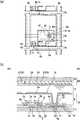
도 1(a), (b)는 각각, 액정 장치(전기 광학 장치)를 그 위에 형성된 각 구성 요소와 함께 대향 기판 쪽에서 본 평면도, 및 그 H-H′ 단면도이다. 도 1(a), (b)에서, 본 형태의 액정 장치(1)는, TN(Twisted Nematic) 모드, ECB(Electrically Controlled Birefringence) 모드, 혹은 VAN(Vertical Aligned Nematic) 모드의 투과형 액티브 매트릭스형 액정 장치이다. 이 액정 장치(1)에서는, 밀폐제(sealant)(22)를 거쳐 소자 기판(10)과 대향 기판(20)이 접합되고, 그 사이에 액정(1f)이 유지되어 있다. 소자 기판(10)에서, 밀폐제(22)의 외측에 위치하는 단부(端部) 영역에는, 데이터선 구동용 IC(60), 및 주사선 구동용 IC(30)가 COG(Chip On Glass) 실장되어 있고, 또한 기판 변을 따라 실장 단자(12)가 형성되어 있다. 밀폐제(22)는, 소자 기판(10)과 대향 기판(20)을 그들 주변에서 접합하기 위한 광경화 수지나 열경화성 수지 등으로 이루어지는 접착제이며, 양 기판 사이의 거리를 소정값으로 하기 위한 유리 섬유(glass fiber), 혹은 유리 비즈(glass beads) 등의 갭 재료(gap material)가 배합되어 있다. 밀폐제(22)에는, 그 끊긴 부분에 의해 액정 주입구(25)가 형성되고, 액정(1f)을 주입한 후, 밀봉재(sealing material)(26)에 의해 밀봉되어 있다.Fig.1 (a), (b) is the top view which looked at the liquid crystal device (electro-optical device) with the each component formed on it on the opposing board | substrate side, respectively, and its HH 'cross section. 1 (a) and (b), the
상세하게는 후술하지만, 소자 기판(10)에는 박막 트랜지스터(1c)나 화소 전극(2a)이 매트릭스 형상으로 형성되고, 그 표면에 배향막(19)이 형성되어 있다. 대향 기판(20)에는, 밀폐제(22)의 내측 영역에 차광성 재료로 이루어지는 프레임(24)(도 1(b)에서는 도시를 생략)이 형성되고, 그 내측이 화상 표시 영역(1a)으로 되어 있다. 대향 기판(20)에는, 도시를 생략하지만, 각 화소의 종횡의 경계 영역과 대향하는 영역에 블랙 매트릭스, 혹은 블랙 스트라이프 등으로 불리는 차광막 이 형성되고, 그 상층 쪽에는, 대향 전극(28) 및 배향막(29)이 형성되어 있다. 도 1(b)에서는 도시를 생략하지만, 대향 기판(20)에서, 소자 기판(10)의 각 화소에 대향하는 영역에는, RGB의 컬러 필터가 그 보호막과 함께 형성되고, 이에 의해, 액정 장치(1)를 모바일 컴퓨터, 휴대 전화기, 액정 텔레비전 등이라고 하는 전자 기기의 컬러 표시 장치로서 이용할 수 있다.Although mentioned later in detail, the
(소자 기판(10)의 구성)(Configuration of Element Substrate 10)
도 2는 도 1 에 나타내는 액정 장치의 소자 기판의 전기적인 구성을 나타내는 설명도이다. 도 2에 나타내는 바와 같이, 소자 기판(10)에는, 화상 표시 영역(1a)에 상당하는 영역에 복수의 소스선(6a)(데이터선) 및 게이트선(3a)(주사선)이 서로 교차하는 방향으로 형성되고, 이들 배선의 교차 부분에 대응하는 위치에 화소(1b)가 구성되어 있다. 게이트선(3a)은 주사선 구동용 IC(30)로부터 연장하고 있으며, 소스선(6a)은 데이터선 구동용 IC(60)로부터 연장하고 있다. 또한, 소자 기판(10)에는, 액정(1f)의 구동을 제어하기 위한 화소 스위칭용 박막 트랜지스터(1c)가 각 화소(1b)에 형성되며, 박막 트랜지스터(1c)의 소스에는 소스선(6a)이 전기적으로 접속되고, 박막 트랜지스터(1c)의 게이트에는 게이트선(3a)이 전기적으로 접속되어 있다.It is explanatory drawing which shows the electrical structure of the element substrate of the liquid crystal device shown in FIG. As shown in FIG. 2, in the
또한, 소자 기판(10)에는, 게이트선(3a)과 병행하여 용량선(3b)이 형성되어 있다. 본 형태에서는, 박막 트랜지스터(1c)에 대하여, 대향 기판(20)과의 사이에 구성된 액정 용량(1g)이 직렬로 접속되어 있고, 또한 액정 용량(1g)에 대하여 병렬 로 유지 용량(1h)이 접속되어 있다. 여기서, 용량선(3b)은, 주사선 구동용 IC(30)에 접속되어 있지만, 정전위로 유지되어 있다. 또, 유지 용량(1h)은, 전단의 게이트선(3a)과의 사이에 구성되는 경우가 있으며, 이 경우, 용량선(3b)은 생략할 수 있다.In addition, the
이와 같이 구성한 액정 장치(1)에서는, 박막 트랜지스터(1c)를 일정 기간만 그 온 상태로 함으로써, 소스선(6a)으로부터 공급되는 화상 신호를 각 화소(1b)의 액정 용량(1g)에 소정의 타이밍에 기입한다. 액정 용량(1g)에 기입된 소정 레벨의 화상 신호는, 액정 용량(1g)에서 일정 기간 유지되고, 또한 유지 용량(1h)은, 액정 용량(1g)에 유지된 화상 신호가 누설되는 것을 방지하고 있다.In the
(각 화소의 구성)(Configuration of Each Pixel)
도 3(a), (b)는 본 발명의 실시예 1에 따른 액정 장치의 화소 하나분의 평면도, 및 A1-B1에 상당하는 위치에서 액정 장치를 절단했을 때의 단면도이다. 도 3(a)에서는, 화소 전극을 굵고 긴 점선으로 나타내고, 게이트선 및 이와 동시 형성된 박막을 가는 실선으로 나타내며, 소스선 및 이와 동시 형성된 박막을 가는 일점 쇄선으로 나타내고, 반도체층을 가늘고 짧은 점선으로 나타낸다. 또, 유지 용량을 구성하는 유전체층에 상당하는 부분에 대해서는 가는 이점 쇄선으로 나타내고, 컨택트 홀에 대해서는, 게이트선 등과 마찬가지로, 가는 실선으로 나타낸다.3 (a) and 3 (b) are a plan view of one pixel of the liquid crystal device according to the first embodiment of the present invention, and sectional views when the liquid crystal device is cut at a position corresponding to A1-B1. In FIG. 3A, the pixel electrode is represented by a thick long dotted line, the gate line and the thin film formed at the same time are represented by a thin solid line, the source line and the thin film formed at the same time are represented by a thin dashed line, and the semiconductor layer is represented by a thin and short dotted line. Indicates. The portion corresponding to the dielectric layer constituting the storage capacitor is represented by a thin double-dot chain line, and the contact hole is represented by a thin solid line like the gate line or the like.
도 3(a)에 나타내는 바와 같이, 소자 기판(10)에서는, 게이트선(3a)과 소스선(6a)으로 둘러싸인 화소 영역(1e)에 화소(1b)를 구성하는 이하의 요소가 구성되 어 있다. 우선, 화소 영역(1e)에는, 하위 게이트형 박막 트랜지스터(1c)의 능동층을 구성하는 아모르파스 실리콘막으로 이루어지는 반도체층(7a)이 형성되어 있다. 또한, 게이트선(3a)으로부터의 돌출 부분에 의해 게이트 전극이 형성되어 있다. 박막 트랜지스터(1c)의 능동층을 구성하는 반도체층(7a) 중, 소스측의 단부에는, 소스선(6a)이 소스 전극으로서 겹치고 있으며, 드레인측의 단부에는 드레인 전극(6b)이 겹치고 있다. 또한, 게이트선(3a)과 병렬하여 용량선(3b)이 형성되어 있다.As shown in FIG. 3A, the
또한, 화소 영역(1e)에는, 용량선(3b)으로부터의 돌출 부분을 하부 전극(3c)으로 하고, 드레인 전극(6b)으로부터의 연설 부분을 상부 전극(6c)으로 하는 유지 용량(1h)이 형성되어 있다. 또한, 상부 전극(6c)에 대해서는, 컨택트 홀(81, 91)을 거쳐, ITO막(Indium Tin Oxide)으로 이루어지는 화소 전극(2a)이 전기적으로 접속되어 있다.Further, in the
이와 같이 구성한 소자 기판(10)의 A1-B1 단면은, 도 3(b)에 나타내는 바와 같이 표시된다. 우선, 유리 기판이나 석영 기판으로 이루어지는 절연 기판(11)상에는, 도전막으로 이루어지는 게이트선(3a)(게이트 전극), 및 용량선(3b)(유지 용량(1h)의 하부 전극(3c))이 형성되어 있다. 본 형태에서, 게이트선(3a) 및 용량선(3b)은 모두, 막 두께가 150㎚인 네오디뮴 함유의 알루미늄 합금막의 상층에 막 두께가 20㎚인 몰리브덴막을 적층한 2층 구조로 되어 있다.The cross section A1-B1 of the
본 형태에서, 게이트선(3a)의 상층 쪽에는 게이트선(3a)을 덮도록 게이트 절연층(4)이 형성되어 있다. 게이트 절연층(4)의 상층 중, 게이트선(3a)의 돌출 부 분(게이트 전극)과 부분적으로 겹치는 영역에는, 박막 트랜지스터(1c)의 능동층을 구성하는 반도체층(7a)이 형성되어 있다. 반도체층(7a) 중, 소스 영역의 상층에는, 도핑된 실리콘막으로 이루어지는 오믹 컨택트층(7b), 및 소스선(6a)이 적층되고, 드레인 영역의 상층에는, 도핑된 실리콘막으로 이루어지는 오믹 컨택트층(7c), 및 드레인 전극(6b)이 형성되어, 박막 트랜지스터(1c)가 구성되어 있다. 또한, 드레인 전극(6b)의 연설 부분에 의해 유지 용량(1h)의 상부 전극(6c)이 형성되어 있다. 본 형태에서, 반도체층(7a)은, 막 두께가 150㎚인 진성 아모르파스 실리콘막으로 이루어지며, 오믹 컨택트층(7b, 7c)은, 인이 도핑된 막 두께가 50㎚인 n+형 아모르파스 실리콘막으로 이루어진다. 소스선(6a) 및 드레인 전극(6b)(상부 전극(6c))은 모두, 하층 쪽으로부터 상층 쪽으로 향하여, 막 두께가 5㎚인 몰리브덴막, 막 두께가 1500㎚인 알루미늄막, 및 막 두께가 50㎚인 몰리브덴막을 적층한 3층 구조를 구비하고 있다.In this embodiment, the
소스선(6a), 드레인 전극(6b), 및 상부 전극(6c)의 상층 쪽에는, 실리콘 질화막 등으로 이루어지는 패시베이션막(8), 및 아크릴 수지 등의 감광성 수지층으로 이루어지는 평탄화막(9)이 각각, 층간 절연막으로서 형성되어 있으며, 평탄화막(9)의 상층에는 화소 전극(2a)이 형성되어 있다. 화소 전극(2a)은, 평탄화막(9)에 형성된 컨택트 홀(91), 및 패시베이션막(8)에 형성된 컨택트 홀(81)을 거쳐 상부 전극(6c)에 전기적으로 접속하고, 상부 전극(6c) 및 드레인 전극(6b)을 거쳐 박막 트랜지스터(1c)의 드레인 영역에 전기적으로 접속하고 있다. 화소 전극(2a)의 표면 에는 배향막(19)이 형성되어 있다. 본 형태에서, 패시베이션막(8)은, 막 두께가 250㎚인 실리콘 질화막으로 이루어지며, 화소 전극(2a)은, 막 두께가 100㎚인 ITO막으로 이루어진다.On the upper layer side of the
이와 같이 구성된 소자 기판(10)에 대향하도록 대향 기판(20)이 배치되고, 소자 기판(10)과 대향 기판(20) 사이에는 액정(1f)이 유지되어 있다. 대향 기판(20)에는, 각 색의 컬러 필터(27), 대향 전극(28) 및 배향막(29)이 형성되어 있으며, 화소 전극(2a)과 대향 전극(28) 사이에 액정 용량(1g)(도 2 참조)이 구성된다. 또, 대향 기판(20) 쪽에는 블랙 매트릭스나 보호막 등이 형성되는 경우가 있지만, 그들 도시를 생략한다.The opposing
(게이트 절연층 및 유전체층의 구성)(Configuration of the gate insulating layer and the dielectric layer)
본 형태의 액정 장치(1)에서, 게이트 절연층(4)은, 하층 쪽이 두꺼운 실리콘 질화막으로 이루어지는 하층 쪽 게이트 절연층(4a)과, 상층 쪽이 얇은 실리콘 질화막으로 이루어지는 상층 쪽 게이트 절연층의 2층 구조로 되어 있다. 본 형태에서, 하층 쪽 게이트 절연층(4a)의 막 두께는, 박막 트랜지스터의 기생 용량의 영향을 작게 하는 두께로 형성되고, 상층 쪽 게이트 절연막의 막 두께는 하층 쪽 게이트 절연막보다 얇게 형성된다. 예컨대, 하층 쪽 게이트 절연막은 250∼500㎚, 바람직하게는 300㎚이며, 상층 쪽 게이트 절연층(4b)의 막 두께는 50∼200㎚, 바람직하게는 100㎚이다. 이들 막 두께는, 박막 트랜지스터의 기입 능력, 기생 용량 및 유지 용량의 밸런스를 고려한 후에 최적화하여 결정할 수 있다. 예컨대, 고화질로 화 소(1b)의 치수가 작은 구조의 경우(예컨대, 한 화소의 짧은 변이 40㎛ 이하), 화소(1c)에서의 유지 용량(1h), 액정 용량(1g)이 작아지지만, 박막 트랜지스터(1c)의 최소 치수는 포토리소그래피의 해상도에 의해 억제된다. 이 때문에, 이러한 고화질 화소에서는, 박막 트랜지스터(1c)의 기생 용량이 한 화소 전체의 용량에서 차지하는 비율이 높아지게 된다. 이 기생 용량의 비율(이하, 기생 용량비)이 커지면, 전기 광학 장치(1)에서는 플릭커(flicker)나, 누화(crosstalk), 소실(burning) 등이라고 하는 표시 품질의 저하를 초래하는 것이 알려져 있으며, 이 기생 용량비가 가능한 한 작아지도록 설계를 행하는 것이 일반적이다. 그러나, 상기한 바와 같은 고화질의 레이아웃에 의해 기생 용량비가 제약을 받는 경우, 종래의 수법에서는, 이를 개선하는 것이 곤란하다. 그런데 본 발명의 구조, 프로세스를 이용하면, 박막 트랜지스터(1c)의 게이트 절연막(4)의 막 두께를 유지 용량(1h)의 측과는 완전히 독립적으로 설정ㆍ제조할 수 있다. 즉, 상기한 고화질 화소에서는, 게이트 절연막을 표준적인 조건보다 두텁게 설정함으로써, 박막 트랜지스터(1c)의 기생 용량을 감소시켜, 기생 용량비를 작게 할 수 있다. 또, 이러한 조건 설정에서는, 박막 트랜지스터(1c)의 전류 구동 능력(화소(1b)로의 신호 기입 능력)이 저하하지만, 고화질 화소는, 기입하는 화소 용량 그 자체가 작아져 있으므로, 이와 같이 게이트 절연막의 두께를 두껍게 하더라도 기입 능력적으로는 문제를 발생하지 않도록 설계를 행할 수 있다.In the
본 형태에서는, 게이트 절연층(4)에서 하층 쪽 게이트 절연층(4a)은, 유지 용량(1h)의 하부 전극(3c) 및 상부 전극(6c)과 평면적으로 겹치는 영역에서 두께 방향의 전체에 걸쳐 제거되어, 개구(41)가 형성되어 있다. 이에 대하여, 상층 쪽 게이트 절연층(4b)은, 대략 전면(全面)에 형성되어 있다. 이 때문에, 게이트 절연층(4)은, 하부 전극(3c) 및 상부 전극(6c)과 평면적으로 겹치는 영역(개구(41)와 평면적으로 겹치는 영역)에, 상층 쪽 게이트 절연층(4b)만으로 이루어지는 막 두께가 얇은 부분을 구비하고 있으며, 이러한 막 두께가 얇은 부분에 의해 유지 용량(1h)의 유전체층(4c)이 구성되어 있다. 여기서, 하부 전극(3c)의 상층 쪽 중, 하부 전극(3c)의 가장자리를 따라 게이트 절연층(4)과 동일 두께인 두꺼운 부분이 남아 있으며, 유전체층(4c)은, 이 두꺼운 절연막으로 둘러싸여 있다. 이 때문에, 하부 전극(3c)의 가장자리 부분이나 상부 전극(6c)의 가장자리 부분에서 발생하기 쉬운 내전압 저하를 방지할 수 있다.In this embodiment, the lower
(액정 장치(1)의 제조 방법)(Manufacturing method of the liquid crystal device 1)
도 4(a)∼(g), 및 도 5(a)∼(d)는, 본 형태의 액정 장치(1)에 이용한 소자 기판(10)의 제조 방법을 나타내는 공정 단면도이다. 또, 소자 기판(10)을 제조하기 위해서는, 소자 기판(10)을 다수 취할 수 있는 대형 기판의 상태에서 이하의 공정이 행해지지만, 이하의 설명에서는, 대형 기판에 대해서도 소자 기판(10)으로 하여 설명한다.4 (a) to 4 (g) and 5 (a) to (d) are cross-sectional views illustrating a method of manufacturing the
우선, 도 4(a)에 나타내는 게이트 전극 형성 공정에서, 대형의 유리 기판 등의 절연 기판(11)의 표면에 금속막(막 두께가 150㎚인 알루미늄 합금막과, 막 두께가 20㎚인 몰리브덴막의 적층막)을 형성한 후, 포토리소그래피 기술을 이용하여 금 속막을 패터닝하고, 게이트선(3a)(게이트 전극), 및 용량선(3b)(하부 전극(3c))을 동시 형성한다.First, in the gate electrode forming step shown in Fig. 4A, a metal film (aluminum alloy film having a film thickness of 150 nm and molybdenum having a film thickness of 20 nm) is formed on the surface of an insulating
다음으로, 게이트 절연층 형성 공정을 행한다. 본 형태에서, 게이트 절연층 형성 공정에서는, 우선, 도 4(b)에 나타내는 하층 쪽 게이트 절연층 형성 공정에서, 플라즈마 CVD법에 의해, 게이트 절연층(4)의 하층 쪽을 구성하는 두꺼운 하층 쪽 게이트 절연층(4a)을 형성한다. 본 형태에서, 하층 쪽 게이트 절연층(4a)은, 막 두께가 약 300㎚인 실리콘 질화막으로 이루어진다.Next, a gate insulating layer forming step is performed. In this embodiment, in the gate insulating layer forming step, first, in the lower gate insulating layer forming step shown in FIG. 4B, the thick lower layer side constituting the lower layer side of the
다음으로, 도 4(c)에 나타내는 하층 쪽 게이트 절연층 에칭 공정에서는, 포토리소그래피 기술을 이용하여, 하부 전극(3c)과 평면적으로 겹치는 영역에 개구를 구비한 레지스트 마스크(도시하지 않음)를 형성한 후, 하층 쪽 게이트 절연층(4a)에 대하여, SF6 등의 불소계 에칭 가스에 의한 반응성 이온 에칭(건식 에칭)을 행하여, 개구(41)를 형성한다. 이러한 반응성 이온 에칭은, 이온의 물리적인 스퍼터 효과와, 래디컬의 화학적인 에칭 효과의 상승 효과를 이용하므로, 이방성에 우수하고, 또한, 높은 생산성을 얻을 수 있다.Next, in the lower gate insulating layer etching step shown in FIG. 4C, a resist mask (not shown) having an opening is formed in a region overlapping with the
다음으로, 도 4(d)에 나타내는 상층 쪽 게이트 절연층 성막 공정에서는, 플라즈마 CVD법에 의해, 게이트 절연층(4)의 상층 쪽을 구성하는 얇은 상층 쪽 게이트 절연층(4b)을 형성한다. 본 형태에서, 상층 쪽 게이트 절연층(4b)은, 막 두께가 약 100㎚인 실리콘 질화막으로 이루어진다. 그 결과, 게이트선(3a)(게이트 전극)의 상층 쪽에는, 두꺼운 하층 쪽 게이트 절연층(4a)과, 얇은 상층 쪽 게이트 절 연층(4b)으로 이루어지는 게이트 절연층(4)이 형성되는 한편, 개구(41)와 평면적으로 겹치는 영역에는, 상층 쪽 게이트 절연층(4b)만으로 이루어지는 유전체층(4c)이 형성된다.Next, in the upper gate insulating layer film forming step shown in FIG. 4 (d), the thin upper
다음으로, 도 4(e)에 나타내는 반도체층 형성 공정에서는, 플라즈마 CVD법에 의해, 막 두께가 150㎚인 진성 아모르파스 실리콘막(7d), 및 막 두께가 50㎚인 n+형 실리콘막(7e)을 연속하여 형성한다. 그 때, 도 4(d)에 나타내는 상층 쪽 게이트 절연층 형성 공정을 행한 소자 기판(10)을 진공 분위기 중으로 유지한 채로, 도 4(e)에 나타내는 반도체층 형성 공정을 행하여, 소자 기판(10)을 대기와 접촉시키지 않는다. 이에 의해, 게이트 절연층(4)(상층 쪽 게이트 절연층(4b))의 표면이 청정한 상태에서 아모르파스 실리콘막(7d)을 적층할 수 있다.Next, in the semiconductor layer forming step shown in Fig. 4E, by the plasma CVD method, an intrinsic
다음으로, 도 4(f)에 나타내는 바와 같이, 포토리소그래피 기술을 이용하여, 아모르파스 실리콘막(7d), 및 n+형 실리콘막(7e)에 에칭을 행하여, 섬 형상의 반도체층(7a), 및 섬 형상의 n+형 실리콘막(7e)을 형성한다. 이 에칭에서도, SF6 등의 불소계 에칭 가스를 이용한 반응성 이온 에칭(건식 에칭)을 행한다.Next, as shown in FIG. 4 (f), the
다음으로, 도 4(g)에 나타내는 바와 같이, 금속막(막 두께가 5㎚인 몰리브덴막, 막 두께가 1500㎚인 알루미늄막, 및 막 두께가 50㎚인 몰리브덴막의 적층막)을 형성한 후, 포토리소그래피 기술을 이용하여 패터닝하여, 소스선(6a), 드레인 전극(6b), 및 상부 전극(6c)을 형성한다. 이어서, 소스선(6a) 및 드레인 전극(6b)을 마스크로서 이용하여, 소스선(6a)과 드레인 전극(6b) 사이의 n+형 실리콘막(7e)을 에칭에 의해 제거하여, 소스ㆍ드레인의 분리를 행한다. 그 결과, 소스선(6a) 및 드레인 전극(6b)이 형성되어 있지 않은 영역으로부터 n+형 실리콘막(7e)이 제거되어 오믹 컨택트층(7b, 7c)이 형성된다. 이 때, 반도체층(7a)의 표면의 일부가 에칭된다. 이렇게 하여, 하위 게이트형의 화소 스위칭용 박막 트랜지스터(1c)가 형성되고, 또한 유지 용량(1h)이 형성된다.Next, as shown in Fig. 4 (g), after forming a metal film (laminated film of molybdenum film having a film thickness of 5 nm, aluminum film having a film thickness of 1500 nm, and molybdenum film having a film thickness of 50 nm), And patterning using photolithography techniques to form the
다음으로, 도 5(a)에 나타내는 바와 같이, 플라즈마 CVD법에 의해, 막 두께가 250㎚인 실리콘 질화막으로 이루어지는 패시베이션막(8)을 형성한다.Next, as shown to Fig.5 (a), the
다음으로, 도 5(b)에 나타내는 바와 같이, 스핀코트법에 의해, 아크릴 수지 등의 감광성 수지를 도포한 후, 노광, 현상하여, 컨택트 홀(91)을 구비한 평탄화막(9)을 형성한다.Next, as shown in FIG.5 (b), after apply | coating photosensitive resin, such as an acrylic resin, by spin coating method, it exposes and develops and the
다음으로, 도 5(c)에 나타내는 바와 같이, 포토리소그래피 기술을 이용하여 패시베이션막(8)에 대하여 에칭을 행하여, 컨택트 홀(91)과 겹치는 위치에 컨택트 홀(81)을 형성한다. 이 에칭에서도, SF6 등의 불소계 에칭 가스를 이용한 반응성 이온 에칭(건식 에칭)을 행한다.Next, as shown in FIG. 5C, the
다음으로, 도 5(d)에 나타내는 바와 같이, 스퍼터법에 의해, 막 두께가 100㎚인 ITO막을 형성한 후, 포토리소그래피 기술 및 습식 에칭을 이용하여 패터닝하여, 화소 전극(2a)을 형성한다. 그 결과, 화소 전극(2a)은, 컨택트 홀(91, 81)을 거쳐 상부 전극(6c)에 전기적으로 접속된다. 이어서, 도 3(b)에 나타내는 배향 막(19)을 형성하기 위한 폴리이미드막을 형성한 후, 연마 처리를 실시한다.Next, as shown in Fig. 5 (d), an ITO film having a thickness of 100 nm is formed by the sputtering method, and then patterned by using photolithography technique and wet etching to form the
이렇게 하여 대형 기판의 상태에서 각종 배선이나 TFT를 형성한 소자 기판(10)에 대해서는, 별도로 형성한 대형의 대향 기판(20)과 밀폐제(22)로 접합한 후, 소정의 사이즈로 절단한다. 이에 의해, 액정 주입구(25)가 개구하므로, 액정 주입구(25)로부터 소자 기판(10)과 대향 기판(20) 사이에 액정(1f)을 주입한 후, 액정 주입구(25)를 밀봉재(26)에 의해 밀봉한다.In this way, the
(본 형태의 주된 효과)(Main effect of this form)
이상 설명한 바와 같이, 본 형태의 액정 장치(1)에서는, 박막 트랜지스터(1c)를 하위 게이트 구조로 구성했으므로, 상층 쪽 게이트 절연막(4b), 능동층(반도체층(7a))을 구성하기 위한 진성 아모르파스 실리콘막(7d), 및 오믹 컨택트층(7b, 7c)을 구성하기 위한 n+형 실리콘막(7e)을 연속 성막할 수 있으므로, 청정한 상층 쪽 게이트 절연막(4b)의 상층에 아모르파스 실리콘막(7d)을 형성할 수 있다. 더구나, 본 형태에서는, 상층 쪽 게이트 절연막(4b), 아모르파스 실리콘막(7d), 및 오믹 컨택트층(7b, 7c)을 구성할 때, 소자 기판(10)을 진공 분위기 중으로 유지를 계속하므로, 상층 쪽 게이트 절연막(4b) 표면의 오염을 확실히 방지할 수 있다. 이 때문에, 게이트 절연층(4)과 반도체층(7a)의 계면이 청정하며, 박막 트랜지스터(1c)의 신뢰성이 높다.As described above, in the
또한, 유지 용량(1h)의 유전체층(4c)의 두께가 게이트 절연층(4)의 두께의 1 /4배이므로, 단위 면적당 정전 용량이 4배이다. 더구나, 유전체층(4c)을 구성하는 상층 쪽 게이트 절연층(4b)은, 실리콘 질화막(유전율이 약 7∼8)이며, 실리콘 산화막보다 유전율이 높으므로, 유지 용량(1h)은, 단위 면적당 정전 용량이 높다. 이 때문에, 유지 용량(1h)은, 전하의 유지 특성이 높은 한편, 단위 면적당 용량값이 높아진 만큼, 그 점유 면적을 축소하면 화소 개구율을 높일 수 있다.In addition, since the thickness of the
또한, 본 형태에서는, 게이트 절연층(4)을 부분적으로 얇게 한 부분을 유지 용량(1h)의 유전체층(4c)으로서 이용하는 데 있어서, 하층 쪽 게이트 절연층(4a)을 남기지 않고, 상층 쪽 게이트 절연층(4b)만으로 유전체층(4c)을 구성했으므로, 하층 쪽 게이트 절연층(4a)을 부분적으로 남기는 경우와 달리, 에칭 깊이의 편차에 기인하는 유지 용량(1h)의 용량 편차를 방지할 수 있다.In addition, in this embodiment, in using the partially thinned portion of the
또한, 본 형태에서는, 게이트 절연층(4)을 부분적으로 얇게 한 부분을 유지 용량(1h)의 유전체층(4c)으로서 이용하는 데 있어서, 하층 쪽 게이트 절연층(4a) 및 상층 쪽 게이트 절연층(4b) 중, 하층 쪽 게이트 절연층(4a)을 제거하고, 이 하층 쪽 게이트 절연층(4a)의 상층에 형성한 상층 쪽 게이트 절연층(4b)을 유지 용량(1h)의 유전체층(4c)으로서 이용한다. 이러한 상층 쪽 게이트 절연층(4b)이라면, 하층 쪽 게이트 절연층(4a)을 건식 에칭에 의해 제거할 때의 정전기나 플라즈마에 노출되지 않으므로, 상층 쪽 게이트 절연층(4b)의 결함 밀도가 낮다. 이 때문에, 유지 용량(1h)의 내전압 저하 등이라고 하는 문제의 발생을 방지할 수 있다. 예컨대, 도 15를 참조하여 설명한 유지 용량(1h)의 유전체층(4c)(하층 쪽 게이트 절연층(4a))은, 정전기나 플라즈마의 영향을 받아 결함 밀도가 0.2개/cm2인 데 대하여, 본 형태의 유지 용량(1h)의 유전체층(4c)(상층 쪽 게이트 절연층(4b))은, 정전기나 플라즈마의 영향을 받지 않으므로, 결함 밀도가 0.01개/cm2로, 현저히 적다. 이러한 결함 밀도는, 2.4인치의 HVGA 방식 액정 패널에 환산하면, 도 15를 참조하여 설명한 유지 용량(1h)을 구비한 액정 장치(1)에서는 불량 발생률이 20%에 상당하는 데 대하여, 본 형태의 유지 용량(1h)을 구비한 액정 장치(1)에 의하면 불량 발생률을 1%까지 감소시킬 수 있게 된다.In this embodiment, the part where the
또, 본 형태에서는, 하층 쪽 게이트 절연층(4a)에 대하여 건식 에칭을 행하여 개구(41)를 형성했지만, 습식 에칭을 행하여 개구(41)를 형성하더라도 좋다. 이러한 경우에도, 상층 쪽 게이트 절연층(4b)은, 하층 쪽 게이트 절연층(4a)에 대한 에칭액에 접촉하지 않으므로, 상층 쪽 게이트 절연층(4b)에 핀홀이 발생하지 않는다. 이 때문에, 유지 용량(1h)의 내전압의 편차를 방지할 수 있다.In this embodiment, although the
(실시예 2)(Example 2)
도 6(a), (b)는 본 발명의 실시예 2에 따른 액정 장치의 화소 하나분의 평면도, 및 A2-B2에 상당하는 위치에서 액정 장치를 절단했을 때의 단면도이다. 도 7(a)~(g)는 본 형태의 액정 장치(1)에 이용한 소자 기판(10)의 제조 공정 중, 소스ㆍ드레인 전극을 형성하기까지의 공정을 나타내는 공정 단면도이다. 도 6(a)에서는, 화소 전극을 굵고 긴 점선으로 나타내고, 게이트선 및 이와 동시 형성된 박막 을 가는 실선으로 나타내며, 소스선 및 이와 동시 형성된 박막을 가는 일점 쇄선으로 나타내고, 반도체층을 가늘고 짧은 점선으로 나타낸다. 또, 유지 용량을 구성하는 유전체층에 상당하는 부분에 대해서는 가는 이점 쇄선으로 나타내고, 컨택트 홀에 대해서는, 게이트선 등과 마찬가지로, 가는 실선으로 나타낸다. 또, 에칭스토퍼층에 대해서는, 굵고 짧은 굵은 선으로 나타낸다. 또, 본 형태의 기본적인 구성은 실시예 1과 마찬가지이므로, 공통하는 부분에는 동일한 부호를 부여하여 그들의 설명을 생략한다.6 (a) and 6 (b) are a plan view of one pixel of the liquid crystal device according to the second embodiment of the present invention, and a cross-sectional view when the liquid crystal device is cut at a position corresponding to A2-B2. 7 (a) to 7 (g) are cross-sectional views illustrating the steps up to forming the source and drain electrodes in the manufacturing process of the
도 6(a), (b)에 나타내는 바와 같이, 본 형태에서도, 실시예 1과 마찬가지로, 소자 기판(101)에서, 게이트선(3a)과 소스선(6a)으로 둘러싸인 화소 영역(1e)에는, 하위 게이트형 박막 트랜지스터(1c)와 유지 용량(1h)이 형성되어 있다. 유지 용량(1h)은, 용량선(3b)으로부터의 돌출 부분을 하부 전극(3c)으로 하고, 드레인 전극(6b)으로부터의 연설 부분을 상부 전극(6c)으로 하고 있다. 게이트 절연층(4)은, 실시예 1과 마찬가지로, 하층 쪽이 두꺼운 실리콘 질화막으로 이루어지는 하층 쪽 게이트 절연층(4a)과, 상층 쪽이 얇은 실리콘 질화막으로 이루어지는 상층 쪽 게이트 절연층의 2층 구조로 되어 있다. 하층 쪽 게이트 절연층(4a)은, 유지 용량(1h)의 하부 전극(3c) 및 상부 전극(6c)과 평면적으로 겹치는 영역에서 두께 방향의 전체에 걸쳐 제거되어, 개구(41)가 형성되어 있다. 이 때문에, 유지 용량(1h)의 유전체층(4c)은, 게이트 절연층(4) 중, 막 두께가 얇은 부분(하층 쪽 게이트 절연층(4a))에 의해 구성되어 있다. 또, 하부 전극(3c)의 상층 쪽 중, 하부 전극(3c)의 가장자리를 따라 게이트 절연층(4)과 동일 두께의 절연막이 형성되어 있으며, 유전체층(4c)은, 이 두꺼운 절연막으로 둘러싸여 있다.As shown in Figs. 6 (a) and 6 (b), also in this embodiment, in the element substrate 101, in the
본 형태에서는, 반도체층(7a)의 상층 쪽 중, 소스선(6a)(소스 전극)의 단부와 드레인 전극(6b)의 단부 사이에 끼워진 영역에 에칭스토퍼층(7x)이 형성되어 있으며, 에칭스토퍼층(7x)의 상층에 덮이도록 오믹 컨택트층(7b, 7c)이 형성되어 있다. 본 형태에서, 에칭스토퍼층(7x)은, 막 두께가 150㎚인 실리콘 질화막으로 이루어진다. 그 밖의 구성은, 실시예 1과 마찬가지이므로, 설명을 생략한다.In this embodiment, the
이러한 구성의 소자 기판(10)을 제조하기 위해서는, 도 7(a)에 나타내는 게이트 전극 형성 공정에서, 절연 기판(11)의 표면에 금속막(알루미늄 합금막과 몰리브덴막의 적층막)을 형성한 후, 포토리소그래피 기술을 이용하여 금속막을 패터닝하여, 게이트선(3a)(게이트 전극), 및 용량선(3b)(하부 전극(3c))을 형성한다.In order to manufacture the
다음으로, 게이트 절연층 형성 공정을 행한다. 본 형태에서도, 실시예 1과 마찬가지로, 도 7(b)에 나타내는 하층 쪽 게이트 절연층 형성 공정에서, 플라즈마 CVD법에 의해, 게이트 절연층(4)의 하층 쪽을 구성하는 두꺼운 실리콘 질화막(하층 쪽 게이트 절연층(4a))을 형성한 후, 하층 쪽 게이트 절연층 에칭 공정에서, 하층 쪽 게이트 절연층(4a)에 대하여 에칭을 행하여, 하부 전극(3c)과 겹치는 위치에 개구(41)를 형성한다. 다음으로, 도 7(c)에 나타내는 상층 쪽 게이트 절연층 형성 공정에서, 게이트 절연층(4)의 상층 쪽을 구성하는 얇은 실리콘 질화막(상층 쪽 게이트 절연층(4b))을 형성한다.Next, a gate insulating layer forming step is performed. Also in this embodiment, similarly to Example 1, in the lower gate insulating layer forming step shown in FIG. 7B, a thick silicon nitride film constituting the lower layer side of the
다음으로, 도 7(d)에 나타내는 반도체층 형성 공정에서, 플라즈마 CVD법에 의해, 진성 아모르파스 실리콘막(7d)을 형성한다. 이 때, 도 7(c)에 나타내는 상 층 쪽 게이트 절연층 형성 공정을 행한 소자 기판(10)에 대해서는, 진공 분위기 중으로 유지한 채로, 도 7(d)에 나타내는 반도체층 형성 공정을 행하여, 소자 기판(10)을 대기와 접촉시키지 않는다. 이에 의해, 게이트 절연층(4)(상층 쪽 게이트 절연층(4b))의 표면이 청정한 상태에서 아모르파스 실리콘막(7d)(능동층)을 적층할 수 있다. 다음으로, 아모르파스 실리콘막(7d)의 상층 쪽에, 막 두께가 150㎚인 실리콘 질화막을 형성한 후, 실리콘 질화막을 에칭하여, 에칭스토퍼층(7x)을 형성한다. 이 에칭에서도, SF6 등의 불소계 에칭 가스를 이용한 반응성 이온 에칭(건식 에칭)을 행한다.Next, in the semiconductor layer forming step shown in FIG. 7 (d), the intrinsic
다음으로, 도 7(e)에 나타내는 바와 같이, 에칭스토퍼층(7x)의 상층 쪽에 n+형 실리콘막(7e)을 형성한다. 다음으로, 도 7(f)에 나타내는 바와 같이, 아모르파스 실리콘막(7d) 및 n+형 실리콘막(7e)에 대하여 포토리소그래피 기술을 이용하여 건식 에칭을 행하여, 섬 형상의 반도체층(7a) 및 n+형 실리콘막(7e)을 형성한다.Next, as shown in FIG.7 (e), the n+
다음으로, 도 7(g)에 나타내는 바와 같이, 금속막(몰리브덴막, 알루미늄막, 및 몰리브덴막의 적층막)을 형성한 후, 포토리소그래피 기술을 이용하여 패터닝하여, 소스선(6a), 드레인 전극(6b), 및 상부 전극(6c)을 형성한다. 이어서, 소스선(6a) 및 드레인 전극(6b)을 마스크로서 이용하여, 소스선(6a)과 드레인 전극(6b) 사이의 n+형 실리콘막(7e)을 에칭에 의해 제거하여, 소스ㆍ드레인의 분리를 행한 다. 그 결과, 소스선(6a) 및 드레인 전극(6b)이 형성되어 있지 않은 영역으로부터 n+형 실리콘막(7e)이 제거되어 오믹 컨택트층(7b, 7c)이 형성된다. 이 때, 에칭스토퍼층(7x)은, 반도체층(7a)을 보호하는 기능을 한다. 이렇게 하여, 하위 게이트형의 화소 스위칭용 박막 트랜지스터(1c)가 형성되고, 또한 유지 용량(1h)이 형성된다. 그 이후의 공정은, 실시예 1과 마찬가지이므로, 설명을 생략한다.Next, as shown in Fig. 7G, a metal film (laminated film of molybdenum film, aluminum film, and molybdenum film) is formed, and then patterned by using photolithography technology, so that the
이와 같이 본 형태에서는, 유지 용량(1h)의 기본적인 구성이 실시예 1과 마찬가지이므로, 신뢰성이 높은 박막 트랜지스터(1c)를 형성할 수 있고, 또한 용량이 높고 내전압이 안정한 유지 용량(1h)을 형성할 수 있는 등, 실시예 1과 마찬가지의 효과를 나타낸다.As described above, in this embodiment, since the basic structure of the
또한, 도 7(d)에 나타내는 바와 같이, 에칭스토퍼층(7x)을 형성할 때, 아모르파스 실리콘막(7d)은, 상층 쪽 게이트 절연층(4b)을 보호하는 기능을 한다. 이 때문에, 에칭스토퍼층(7x)을 형성한 경우에도, 유전체층(4c)으로서 이용되는 상층 쪽 게이트 절연층(4b)에 결함이 발생하는 것을 방지할 수 있다.As shown in Fig. 7D, when forming the
(실시예 3)(Example 3)
도 8(a), (b)는 본 발명의 실시예 3에 따른 액정 장치의 화소 하나분의 평면도, 및 A3-B3에 상당하는 위치에서 액정 장치를 절단했을 때의 단면도이다. 도 9(a)∼(g)는 본 형태의 액정 장치(1)에 이용한 소자 기판(10)의 제조 공정 중, 소스ㆍ드레인 전극을 형성하기까지의 공정을 나타내는 공정 단면도이다. 도 8(a)에 서는, 화소 전극을 굵고 긴 점선으로 나타내고, 게이트선 및 이와 동시 형성된 박막을 가는 실선으로 나타내며, 소스선 및 이와 동시 형성된 박막을 가는 일점 쇄선으로 나타내고, 반도체층을 가늘고 짧은 점선으로 나타낸다. 또한, 유지 용량을 구성하는 유전체층에 상당하는 부분에 대해서는 가는 이점 쇄선으로 나타내고, 컨택트 홀에 대해서는, 게이트선 등과 마찬가지로, 가는 실선으로 나타낸다. 또한, 유지 용량의 상부 전극에 대해서는, 굵은 일점 쇄선으로 나타낸다. 또, 본 형태의 기본적인 구성은, 실시예 1과 마찬가지이므로, 공통하는 부분에는 동일한 부호를 부여하여 그들의 설명을 생략하다.8A and 8B are a plan view of one pixel of the liquid crystal device according to the third embodiment of the present invention, and sectional views when the liquid crystal device is cut at a position corresponding to A3-B3. 9A to 9G are cross-sectional views showing the steps up to forming the source and drain electrodes in the manufacturing process of the
도 8(a), (b)에 나타내는 바와 같이, 본 형태에서도, 실시예 1과 마찬가지로, 소자 기판(10)에서, 게이트선(3a)과 소스선(6a)으로 둘러싸인 화소 영역(1e)에는, 하위 게이트형의 박막 트랜지스터(1c)와, 유지 용량(1h)이 형성되어 있다.As shown in Figs. 8A and 8B, in this embodiment, in the
본 형태에서, 유지 용량(1h)은, 용량선(3b)으로부터의 돌출 부분을 하부 전극(3c)으로 하고 있는 점에서는 실시예 1과 마찬가지이다. 단, 유지 용량(1h)의 상부 전극(5a)은, 게이트 절연층(4)과 드레인 전극(6b)의 층간에 형성된 ITO막에 의해 구성되어 있으며, 상부 전극(5a)은, 드레인 전극(6b)과의 부분적인 중첩 부분에 의해 드레인 전극(6b)에 전기적으로 접속되어 있다. 본 형태에서, 상부 전극(5a)을 구성하는 ITO막의 막 두께는 50㎚이다. 또, 상부 전극(5a)에 대해서는, 컨택트 홀(81, 91)을 거쳐, 평탄화막(9)의 상층에 형성된 화소 전극(2a)이 전기적으로 접속되어 있다.In this embodiment, the
게이트 절연층(4)은, 실시예 1과 마찬가지로, 하층 쪽이 두꺼운 실리콘 질화 막으로 이루어지는 하층 쪽 게이트 절연층(4a)과, 상층 쪽이 얇은 실리콘 질화막으로 이루어지는 상층 쪽 게이트 절연층의 2층 구조로 되어 있다. 하층 쪽 게이트 절연층(4a)은, 유지 용량(1h)의 하부 전극(3c) 및 상부 전극(5a)과 평면적으로 겹치는 영역에서 두께 방향의 전체에 걸쳐 제거되어, 개구(41)가 형성되어 있다. 이 때문에, 유지 용량(1h)의 유전체층(4c)은, 게이트 절연층(4) 중, 막 두께가 얇은 부분(하층 쪽 게이트 절연층(4a))에 의해 구성되어 있다. 또, 하부 전극(3c)의 상층 쪽 중, 하부 전극(3c)의 가장자리를 따라 게이트 절연층(4)과 동일 두께의 절연막이 형성되어 있으며, 유전체층(4c)은, 이 두꺼운 절연막으로 둘러싸여 있다. 그 밖의 구성은, 실시예 1과 마찬가지이므로, 설명을 생략한다.As in the first embodiment, the
이러한 구성의 소자 기판(10)을 제조하기 위해서는, 도 9(a)에 나타내는 게이트 전극 형성 공정에서, 절연 기판(11)의 표면에 금속막(알루미늄 합금막과 몰리브덴막의 적층막)을 형성한 후, 포토리소그래피 기술을 이용하여 금속막을 패터닝하여, 게이트선(3a)(게이트 전극), 및 용량선(3b)(하부 전극(3c))을 형성한다.In order to manufacture the
다음으로, 게이트 절연층 형성 공정을 행한다. 본 형태에서도, 실시예 1과 마찬가지로, 도 9(b)에 나타내는 하층 쪽 게이트 절연층 형성 공정에서, 플라즈마 CVD법에 의해, 게이트 절연층(4)의 하층 쪽을 구성하는 두꺼운 실리콘 질화막(하층 쪽 게이트 절연층(4a))을 형성한 후, 하층 쪽 게이트 절연층 에칭 공정에서, 하층 쪽 게이트 절연층(4a)에 대하여 에칭을 행하여, 하부 전극(3c)과 겹치는 위치에 개구(41)를 형성한다. 다음으로, 도 9(c)에 나타내는 상층 쪽 게이트 절연층 성막 공정에서, 게이트 절연층(4)의 상층 쪽을 구성하는 얇은 실리콘 질화막(상층 쪽 게 이트 절연층(4b))을 형성한다.Next, a gate insulating layer forming step is performed. Also in this embodiment, similarly to Example 1, in the lower gate insulating layer forming step shown in FIG. 9B, a thick silicon nitride film constituting the lower layer side of the
다음으로, 도 9(d)에 나타내는 반도체층 형성 공정에서, 진성 아모르파스 실리콘막(7d), 및 n+형 실리콘막(7e)을 순차적으로 형성한다. 이 때, 도 9(c)에 나타내는 상층 쪽 게이트 절연층 형성 공정을 행한 소자 기판(10)에 대해서는, 진공 분위기 중으로 유지한 채로, 도 9(d)에 나타내는 반도체층 형성 공정을 행하여, 소자 기판(10)을 대기와 접촉시키지 않는다. 이에 의해, 게이트 절연층(4)(상층 쪽 게이트 절연층(4b))의 표면이 청정한 상태에서 아모르파스 실리콘막(7d)(능동층)을 적층할 수 있다.Next, in the semiconductor layer forming step shown in FIG. 9D, the intrinsic
다음으로, 도 9(e)에 나타내는 바와 같이, 포토리소그래피 기술을 이용하여, 아모르파스 실리콘막(7d), 및 n+형 실리콘막(7e)에 건식 에칭을 행하여, 섬 형상의 반도체층(7a), 및 섬 형상의 n+형 실리콘막(7e)을 형성한다.Next, as shown in Fig. 9E, dry etching is performed on the
다음으로, 도 9(f)에 나타내는 상부 전극 형성 공정에서, 스퍼터법에 의해, 막 두께가 50㎚인 ITO막을 형성한 후, 포토리소그래피 기술을 이용하여, ITO막에 습식 에칭을 행하여, 상부 전극(5a)을 형성한다. 이렇게 하여, 유지 용량(1h)이 형성된다.Next, in the upper electrode forming step shown in FIG. 9 (f), after forming an ITO film having a film thickness of 50 nm by the sputtering method, wet etching is performed on the ITO film using a photolithography technique to obtain the upper electrode. (5a) is formed. In this way, the holding
다음으로, 도 9(g)에 나타내는 바와 같이, 금속막(몰리브덴막, 알루미늄막, 및 몰리브덴막의 적층막)을 형성한 후, 포토리소그래피 기술을 이용하여 패터닝하여, 소스선(6a), 드레인 전극(6b), 및 상부 전극(6c)을 형성한다. 이어서, 소스선(6a) 및 드레인 전극(6b)을 마스크로서 이용하여, 소스선(6a)과 드레인 전극(6b) 사이의 n+형 실리콘막(7e)을 에칭에 의해 제거하고, 소스ㆍ드레인의 분리를 행한다. 그 결과, 소스선(6a) 및 드레인 전극(6b)이 형성되어 있지 않은 영역으로부터 n+형 실리콘막(7e)이 제거되어 오믹 컨택트층(7b, 7c)이 형성된다. 이렇게 하여, 하위 게이트형의 화소 스위칭용 박막 트랜지스터(1c)가 형성된다. 그 이후의 공정은, 실시예 1과 마찬가지이므로, 설명을 생략한다.Next, as shown in Fig. 9G, a metal film (laminated film of molybdenum film, aluminum film, and molybdenum film) is formed, and then patterned by using photolithography technology, so that the
이와 같이 본 형태에서는, 유지 용량(1h)의 기본적인 구성이 실시예 1과 마찬가지이므로, 신뢰성이 높은 박막 트랜지스터(1c)를 형성할 수 있고, 또한 용량이 높고 내전압이 안정한 유지 용량(1h)을 형성할 수 있는 등, 실시예 1과 마찬가지의 효과를 나타낸다.As described above, in this embodiment, since the basic structure of the
또한, 상부 전극(5a)으로서 ITO막(투명 전극)을 이용했으므로, 드레인 전극(6b)의 연설 부분을 상부 전극으로서 이용한 경우와 비교하여, 화소 개구율을 높일 수 있다.In addition, since the ITO film (transparent electrode) was used as the
(실시예 4)(Example 4)
도 10(a), (b)는 본 발명의 실시예 4에 따른 액정 장치의 화소 하나분의 평면도, 및 A4-B4에 상당하는 위치에서 액정 장치를 절단했을 때의 단면도이다. 도 11(a)∼(g)는 본 형태의 액정 장치(1)에 이용한 소자 기판(10)의 제조 공정 중, 소스ㆍ드레인 전극을 형성하기까지의 공정을 나타내는 공정 단면도이다. 도 10(a)에서는, 화소 전극을 굵고 긴 점선으로 나타내고, 게이트선 및 이와 동시 형성된 박 막을 가는 실선으로 나타내며, 소스선 및 이와 동시 형성된 박막을 가는 일점 쇄선으로 나타내고, 반도체층을 가늘고 짧은 점선으로 나타낸다. 또, 유지 용량을 구성하는 유전체층에 상당하는 부분에 대해서는 가는 이점 쇄선으로 나타내고, 컨택트 홀에 대해서는, 게이트선 등과 마찬가지로, 가는 실선으로 나타낸다. 또, 본 형태의 기본적인 구성은, 실시예 1과 마찬가지이므로, 공통하는 부분에는 동일한 부호를 부여하여 그들의 설명을 생략한다.10 (a) and 10 (b) are a plan view of one pixel of the liquid crystal device according to the fourth embodiment of the present invention and a cross-sectional view when the liquid crystal device is cut at a position corresponding to A4-B4. 11A to 11G are cross-sectional views illustrating the steps up to forming the source and drain electrodes in the manufacturing process of the
도 10(a), (b)에 나타내는 바와 같이, 본 형태에서도, 실시예 1과 같이 소자 기판(10)에서, 게이트선(3a)과 소스선(6a)으로 둘러싸인 화소 영역(1e)에는, 하위 게이트형의 박막 트랜지스터(1c)와, 유지 용량(1h)이 형성되어 있다. 단, 실시예 1∼3과 달리, 본 형태에서는, 평탄화막이 형성되어 있지 않고, 화소 전극(2a)은, 게이트 절연층(4)과 드레인 전극(6b)의 층간에 형성되며, 드레인 전극(6b)과의 부분적인 중첩 부분에 의해 드레인 전극(6b)에 전기적으로 접속되어 있다.As shown in Figs. 10 (a) and 10 (b), also in this embodiment, in the
또한, 유지 용량(1h)은, 용량선(3b)으로부터의 돌출 부분을 하부 전극(3c)으로 하고 있는 점에서는 실시예 1과 마찬가지이다. 단, 유지 용량(1h)의 상부 전극은, 화소 전극(2a) 중, 하부 전극(3c)과 평면적으로 겹치는 부분에 의해 구성되어 있다.The
게이트 절연층(4)은, 실시예 1과 마찬가지로, 하층 쪽이 두꺼운 실리콘 질화막으로 이루어지는 하층 쪽 게이트 절연층(4a)과, 상층 쪽이 얇은 실리콘 질화막으로 이루어지는 상층 쪽 게이트 절연층의 2층 구조로 되어 있다. 하층 쪽 게이트 절연층(4a)은, 유지 용량(1h)의 하부 전극(3c) 및 화소 전극(2a)과 평면적으로 겹 치는 영역에서 두께 방향의 전체에 걸쳐 제거되어, 개구(41)가 형성되어 있다. 이 때문에, 유지 용량(1h)의 유전체층(4c)은, 게이트 절연층(4) 중, 막 두께가 얇은 부분(하층 쪽 게이트 절연층(4a))에 의해 구성되어 있다. 또, 하부 전극(3c)의 상층 쪽 중, 하부 전극(3c)의 가장자리를 따라 게이트 절연층(4)과 동일 두께의 절연막이 형성되어 있으며, 유전체층(4c)은, 이 두꺼운 절연막으로 둘러싸여 있다. 그 밖의 구성은, 실시예 1과 마찬가지이므로, 설명을 생략한다.The
이러한 구성의 소자 기판(10)을 제조하기 위해서는, 도 11(a)에 나타내는 게이트 전극 형성 공정에서, 절연 기판(11)의 표면에 금속막(알루미늄 합금막과 몰리브덴막의 적층막)을 형성한 후, 포토리소그래피 기술을 이용하여 금속막을 패터닝하여, 게이트선(3a)(게이트 전극), 및 용량선(3b)(하부 전극(3c))을 형성한다.In order to manufacture the
다음으로, 게이트 절연층 형성 공정을 행한다. 본 형태에서도, 실시예 1과 마찬가지로, 도 11(b)에 나타내는 하층 쪽 게이트 절연층 형성 공정에서, 플라즈마 CVD법에 의해, 게이트 절연층(4)의 하층 쪽을 구성하는 두꺼운 실리콘 질화막(하층 쪽 게이트 절연층(4a))을 형성한 후, 하층 쪽 게이트 절연층 에칭 공정에서, 하층 쪽 게이트 절연층(4a)에 대하여 에칭을 행하여, 하부 전극(3c)과 겹치는 위치에 개구(41)를 형성한다. 다음으로, 도 11(c)에 나타내는 상층 쪽 게이트 절연층 성막 공정에서, 게이트 절연층(4)의 상층 쪽을 구성하는 얇은 실리콘 질화막(상층 쪽 게이트 절연층(4b))을 형성한다.Next, a gate insulating layer forming step is performed. Also in this embodiment, in the lower gate insulating layer forming step shown in FIG. 11 (b) as in the first embodiment, a thick silicon nitride film constituting the lower layer side of the
다음으로, 도 11(d)에 나타내는 반도체층 형성 공정에서, 진성 아모르파스 실리콘막(7d), 및 n+형 실리콘막(7e)을 순차적으로 형성한다. 이 때, 도 11(c)에 나타내는 상층 쪽 게이트 절연층 형성 공정을 행한 소자 기판(10)에 대해서는, 진공 분위기 중으로 유지한 채로, 도 11(d)에 나타내는 반도체층 형성 공정을 행하여, 소자 기판(10)을 대기와 접촉시키지 않는다. 이에 의해, 게이트 절연층(4)(상층 쪽 게이트 절연층(4b))의 표면이 청정한 상태에서 아모르파스 실리콘막(7d)(능동층)을 적층할 수 있다.Next, in the semiconductor layer forming step shown in FIG. 11D, the intrinsic
다음으로, 도 11(e)에 나타내는 바와 같이, 포토리소그래피 기술을 이용하여, 아모르파스 실리콘막(7d), 및 n+형 실리콘막(7e)에 건식 에칭을 행하여, 섬 형상의 반도체층(7a), 및 섬 형상의 n+형 실리콘막(7e)을 형성한다.Next, as shown in FIG. 11E, dry etching is performed on the
다음으로, 도 11(f)에 나타내는 화소 전극 형성 공정(상부 전극 형성 공정)에서, ITO막을 형성한 후, 포토리소그래피 기술을 이용하여, ITO막에 에칭을 행하여, 화소(2a)를 형성한다. 이렇게 하여, 유지 용량(1h)이 형성된다.Next, in the pixel electrode formation process (upper electrode formation process) shown in FIG. 11 (f), after forming an ITO film, the ITO film is etched using photolithography technique to form the
다음으로, 도 11(g)에 나타내는 바와 같이, 금속막(몰리브덴막, 알루미늄막, 및 몰리브덴막의 적층막)을 형성한 후, 포토리소그래피 기술을 이용하여 패터닝하여, 소스선(6a), 드레인 전극(6b), 및 상부 전극(6c)을 형성한다. 이어서, 소스선(6a) 및 드레인 전극(6b)을 마스크로서 이용하여, 소스선(6a)과 드레인 전극(6b) 사이의 n+형 실리콘막(7e)을 에칭에 의해 제거하여, 소스ㆍ드레인의 분리를 행한다. 그 결과, 소스선(6a) 및 드레인 전극(6b)이 형성되어 있지 않은 영역으로부터 n+형 실리콘막(7e)이 제거되어 오믹 컨택트층(7b, 7c)이 형성된다. 이렇게 하여, 하위 게이트형의 화소 스위칭용 박막 트랜지스터(1c)가 형성된다. 그 이후의 공정은, 실시예 1과 마찬가지이므로, 설명을 생략한다.Next, as shown in Fig. 11G, a metal film (laminated film of molybdenum film, aluminum film, and molybdenum film) is formed, and then patterned by using photolithography technology, so that the
이와 같이 본 형태에서는, 유지 용량(1h)의 기본적인 구성이 실시예 1과 마찬가지이므로, 신뢰성이 높은 박막 트랜지스터(1c)를 형성할 수 있고, 또한 용량이 높고 내전압이 안정한 유지 용량(1h)을 형성할 수 있는 등, 실시예 1과 마찬가지의 효과를 나타낸다.As described above, in this embodiment, since the basic structure of the
또한, 유지 용량(1h)의 상부 전극으로서, ITO막(투명 전극)으로 이루어지는 화소 전극(2a)의 일부를 이용했으므로, 드레인 전극(6b)의 연설 부분을 상부 전극으로서 이용한 경우와 비교하여, 화소 개구율을 높일 수 있다.In addition, since a part of the
(실시예 5)(Example 5)
도 12(a), (b)는 본 발명의 실시예 5에 따른 액정 장치의 화소 하나분의 평면도, 및 A5-B5에 상당하는 위치애서 액정 장치를 절단했을 때의 단면도이다. 도 12(a)에서는, 화소 전극을 굵고 긴 점선으로 나타내고, 게이트선 및 이와 동시 형성된 박막을 가는 실선으로 나타내며, 소스선 및 이와 동시 형성된 박막을 가는 일점 쇄선으로 나타내고, 반도체층을 가늘고 짧은 점선으로 나타낸다. 또, 유지 용량을 구성하는 유전체층에 상당하는 부분에 대해서는 가는 이점 쇄선으로 나타내고, 컨택트 홀에 대해서는, 게이트선 등과 마찬가지로, 가는 실선으로 나타낸다. 또, 본 형태의 기본적인 구성은, 실시예 1과 마찬가지이므로, 공통하는 부분에는 동일한 부호를 부여하여 그들의 설명을 생략한다.12A and 12B are a plan view of one pixel of the liquid crystal device according to the fifth embodiment of the present invention, and sectional views when the liquid crystal device is cut at positions corresponding to A5-B5. In FIG. 12A, the pixel electrode is represented by a thick long dotted line, the gate line and the thin film formed at the same time are represented by a thin solid line, the source line and the thin film formed at the same time are represented by a thin dashed line, and the semiconductor layer is represented by a thin and short dotted line. Indicates. The portion corresponding to the dielectric layer constituting the storage capacitor is represented by a thin double-dot chain line, and the contact hole is represented by a thin solid line like the gate line or the like. In addition, since the basic structure of this embodiment is the same as that of Example 1, the same code | symbol is attached | subjected to a common part and their description is abbreviate | omitted.
도 12(a), (b)에 나타내는 바와 같이, 본 형태에서도, 실시예 1과 마찬가지로, 소자 기판(10)에서, 게이트선(3a)과 소스선(6a)으로 둘러싸인 화소 영역(1e)에는, 하위 게이트형의 박막 트랜지스터(1c)와, 유지 용량(1h)이 형성되어 있다. 단, 실시예 1∼4와 달리, 본 형태에서는, 용량선이 형성되어 있지 않고, 주사 방향(게이트선(3a)의 연장 방향과 교차하는 방향/소스선(6a)의 연장 방향)에서의 전단측의 게이트선(3a)의 일부에 의해 유지 용량(1h)의 하부 전극(3c)이 구성되어 있다.As shown in Figs. 12 (a) and 12 (b), also in this embodiment, in the
또한, 유지 용량(1h)에서는, 하부 전극(3c)과 겹치는 영역에 상부 전극(6d)이 형성되어 있으며, 본 형태에서는, 상부 전극(6d)으로서는, 소스선(6a)이나 드레인 전극(6b)과 동시 형성된 금속층이 이용되고 있다. 여기서, 상부 전극(6d)은, 드레인 전극(6b)과 분리하여 형성되어 있다. 이 때문에, 평탄화막(9)의 상층에 형성된 화소 전극(2a)은, 패시베이션막(8)의 컨택트 홀(81), 및 평탄화막(9)의 컨택트 홀(91)을 거쳐 상부 전극(6d)에 전기적으로 접속하고, 패시베이션막(8)의 컨택트 홀(82), 및 평탄화막(9)의 컨택트 홀(92)을 거쳐 드레인 전극(6b)에 전기적으로 접속하고 있다.In the
게이트 절연층(4)은, 실시예 1과 마찬가지로, 하층 쪽이 두꺼운 실리콘 질화막으로 이루어지는 하층 쪽 게이트 절연층(4a)과, 상층 쪽이 얇은 실리콘 질화막으로 이루어지는 상층 쪽 게이트 절연층의 2층 구조로 되어 있다. 하층 쪽 게이트 절연층(4a)은, 유지 용량(1h)의 하부 전극(3c) 및 상부 전극(6d)과 평면적으로 겹치는 영역에서 두께 방향의 전체에 걸쳐 제거되어, 개구(41)가 형성되어 있다. 이 때문에, 유지 용량(1h)의 유전체층(4c)은, 게이트 절연층(4) 중, 막 두께가 얇은 부분(하층 쪽 게이트 절연층(4a))에 의해 구성되어 있다. 또, 하부 전극(3c)의 상층 쪽 중, 하부 전극(3c)의 가장자리를 따라 게이트 절연층(4)과 동일 두께의 절연막이 형성되어 있으며, 유전체층(4c)은, 이 두꺼운 절연막으로 둘러싸여 있다. 그 밖의 구성은, 실시예 1과 마찬가지이므로, 설명을 생략한다.The
이러한 구성의 소자 기판(10)은, 기본적으로는 실시예 1과 마찬가지인 방법으로 제조할 수 있다. 즉, 도 4(a)에 나타내는 게이트 전극 형성 공정에서는, 용량선을 형성하지 않고, 또한 게이트선(3a)을 도 12(a)에 나타내는 평면 형상으로 형성한다. 또한, 도 4(g)에 나타내는 소스ㆍ드레인 전극 형성 공정에서 소스선(6a) 및 드레인 전극(6b)을 형성할 때, 상부 전극(6d)을 형성한다. 또한, 도 5(b)에 나타내는 평탄화막 형성 공정에서는, 컨택트 홀(91, 92)을 구비한 평탄화막(9)을 형성하고, 또한 도 5(c)에 나타내는 컨택트 홀 형성 공정에서는, 포토리소그래피 기술을 이용하여 패시베이션막(8)에 대하여 에칭을 행할 때, 컨택트 홀(91, 92)과 겹치는 위치에 컨택트 홀(81, 82)을 형성한다.The
(그 밖의 실시예)(Other Embodiments)
상기 실시예에서는, 게이트 절연층(4)을 구성하는 하층 쪽 게이트 절연층(4a) 및 상층 쪽 게이트 절연층(4b)의 모두가 동일한 절연막으로 이루어지는 구 성이었지만, 하층 쪽 게이트 절연층(4a) 및 상층 쪽 게이트 절연층(4b)이 서로 다른 절연막으로 이루어지는 구성이더라도 좋다. 이 경우, 게이트 절연층(4)을 실리콘 산화막과 실리콘 질화막에 의해 구성하는 경우, 유전체층(4c)으로서 이용하는 상층 쪽 게이트 절연층(4b)에 대해서는 유전율이 높은 실리콘 질화막에 의해 구성하는 것이 바람직하다. 또한, 상기 실시예에서는, 하층 쪽 게이트 절연층(4a) 및 상층 쪽 게이트 절연층(4b)은 각각, 1층의 절연막으로 이루어지는 구성이었지만, 하층 쪽 게이트 절연층(4a) 및 상층 쪽 게이트 절연층(4b)이 각각, 복수층의 절연막으로 이루어지는 구성이더라도 좋다.In the above embodiment, although both the lower
상기 실시예에서는, 게이트 절연층(4)을 부분적으로 얇게 한 부분을 유지 용량(1h)의 유전체층(4c)으로서 이용하는 데 있어서, 하부 전극(3c)의 바깥쪽 둘레의 가장자리보다 내측 영역에서만 하층 쪽 게이트 절연층(4a)을 제거하여 개구(41)를 형성했지만, 하부 전극(3c)의 가장자리 부분이나 상부 전극의 가장자리 부분에서 발생하기 쉬운 내전압 저하가 문제가 되지 않는 경우나, 다른 대책이 실시되고 있는 경우에는, 하부 전극(3c)이나 상부 전극보다 넓은 영역에 걸쳐 하층 쪽 게이트 절연층(4a)을 제거하더라도 좋다.In the above embodiment, in using the partially thinned portion of the
상기 실시예에서는, 게이트선(3a)에 알루미늄 합금막과 몰리브덴막의 다층막을 이용하고, 소스선(6a)에 알루미늄막과 몰리브덴막의 다층막을 이용했지만, 이들 배선에는 그 밖의 금속막을 이용할 수 있고, 또한, 실리사이드막 등이라고 하는 도전막을 이용하여도 좋다. 또한, 상기 실시예에서는 반도체층(7a)으로서 진성 아모르파스 실리콘막을 이용했지만, 그 밖의 실리콘막이나, 유기 반도체막, 산화아연 등의 투명 반도체막을 이용하여도 좋다.In the above embodiment, a multilayer film of an aluminum alloy film and a molybdenum film is used for the
또한, 상기 실시예에서는, 투과형 액정 장치를 예로 설명했지만, 반투과 반사형 액정 장치나 전반사형 액정 장치에 본 발명을 적용하더라도 좋다. 또한, 상기 실시예에서는, TN 모드, ECB 모드, VAN 모드의 액티브 매트릭스형 액정 장치를 예로 설명했지만, IPS(In-Plane Switching) 모드 등의 다른 모드를 본 발명의 액정 장치(전기 광학 장치)에 적용하더라도 좋다.In addition, in the said embodiment, although the transmissive liquid crystal device was demonstrated to the example, you may apply this invention to a transflective liquid crystal device or a total reflection type liquid crystal device. In the above embodiment, the active matrix liquid crystal device of the TN mode, the ECB mode, and the VAN mode has been described as an example, but other modes such as an IPS (In-Plane Switching) mode may be applied to the liquid crystal device (electro-optical device) of the present invention. You may apply.
또한, 전기 광학 장치로서 액정 장치에 한하지 않고, 예컨대, 유기 EL(electroluminescence) 장치에서도, 유기 EL막을 전기 광학 물질로서 유지하는 소자 기판상의 각 화소 영역에, 박막 트랜지스터와, 이 박막 트랜지스터에 전기적으로 접속된 화소 전극과, 상기 박막 트랜지스터의 게이트 절연층보다 하층 쪽에 하부 전극을 구비하는 유지 용량이 형성되므로, 이러한 유기 EL 장치에 본 발명을 적용하더라도 좋다.In addition to the liquid crystal device as the electro-optical device, for example, even in an organic EL (electroluminescence) device, the thin film transistor and the thin film transistor are electrically connected to each pixel region on the element substrate holding the organic EL film as the electro-optic material. Since the storage capacitor which has the connected pixel electrode and the lower electrode below the gate insulating layer of the said thin film transistor is formed, you may apply this invention to such organic electroluminescent apparatus.
(전자 기기의 실시예)(Example of an electronic device)
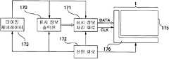
도 13은 본 발명에 따른 액정 장치를 각종 전자 기기의 표시 장치로서 이용하는 경우의 일실시예를 나타내고 있다. 여기에 나타내는 전자 기기는, 퍼스널 컴퓨터나 휴대 전화기 등이며, 표시 정보 출력원(170), 표시 정보 처리 회로(171), 전원 회로(172), 타이밍 제네레이터(173), 그리고 액정 장치(1)를 갖는다. 또한, 액정 장치(1)는, 패널(175) 및 구동 회로(176)를 갖고 있으며, 상술한 액정 장치(1)를 이용할 수 있다. 표시 정보 출력원(170)은, ROM(Read Only Memory), RAM(Random Access Memory) 등이라고 하는 메모리, 각종 디스크 등이라고 하는 기억 장치, 디지털 화상 신호를 동조 출력하는 동조 회로 등을 구비하고, 타이밍 제네레이터(173)에 의해 생성된 각종 클록 신호에 근거하여, 소정 형식의 화상 신호 등이라고 하는 표시 정보를 표시 정보 처리 회로(171)에 공급한다. 표시 정보 처리 회로(171)는, 직렬-병렬 변환 회로나, 증폭ㆍ반전 회로, 로테이션 회로, 감마 보정 회로, 클램프 회로 등이라고 하는 주지의 각종 회로를 구비하고, 입력한 표시 정보의 처리를 실행하여, 그 화상 신호를 클록 신호 CLK와 함께 구동 회로(176)에 공급한다. 전원 회로(172)는, 각 구성 요소에 소정의 전압을 공급한다.13 illustrates an embodiment in which the liquid crystal device according to the present invention is used as a display device of various electronic devices. The electronic apparatus shown here is a personal computer, a mobile phone, etc., and the display
상기한 본 발명에 따르면, 게이트 절연층을 부분적으로 얇게 한 부분을 유지 용량의 유전체층으로서 이용한 경우에도, 유지 용량의 용량 편차나 유지 용량의 내전압 저하를 억제할 수 있는 전기 광학 장치, 전자 기기, 및 전기 광학 장치의 제조 방법을 제공할 수 있다.According to the present invention described above, an electro-optical device, an electronic device capable of suppressing a variation in capacitance of a storage capacitor and a drop in the breakdown voltage of the storage capacitor, even when a portion in which the gate insulating layer is partially thinned as the dielectric layer of the storage capacitor, and It is possible to provide a method for producing an electro-optical device.
Claims (11)
Translated fromKoreanApplications Claiming Priority (2)
| Application Number | Priority Date | Filing Date | Title |
|---|---|---|---|
| JP2006121641AJP2007294709A (en) | 2006-04-26 | 2006-04-26 | Electro-optical device, electronic apparatus, and method of manufacturing electro-optical device |
| JPJP-P-2006-00121641 | 2006-04-26 |
Publications (2)
| Publication Number | Publication Date |
|---|---|
| KR20070105925Atrue KR20070105925A (en) | 2007-10-31 |
| KR100884118B1 KR100884118B1 (en) | 2009-02-17 |
Family
ID=38191872
Family Applications (1)
| Application Number | Title | Priority Date | Filing Date |
|---|---|---|---|
| KR1020070040991AExpired - Fee RelatedKR100884118B1 (en) | 2006-04-26 | 2007-04-26 | Electro-optical devices, electronic devices, and methods of manufacturing electro-optical devices |
Country Status (6)
| Country | Link |
|---|---|
| US (1) | US20070252152A1 (en) |
| EP (1) | EP1850386A1 (en) |
| JP (1) | JP2007294709A (en) |
| KR (1) | KR100884118B1 (en) |
| CN (1) | CN100547802C (en) |
| TW (1) | TW200742089A (en) |
Cited By (3)
| Publication number | Priority date | Publication date | Assignee | Title |
|---|---|---|---|---|
| US7994500B2 (en) | 2008-06-30 | 2011-08-09 | Samsung Mobile Display Co., Ltd. | Thin film transistor, method of manufacturing the same and flat panel display device having the same |
| KR101113354B1 (en)* | 2010-04-16 | 2012-02-29 | 삼성모바일디스플레이주식회사 | Display device and fabrication method of the same |
| US8148779B2 (en) | 2008-06-30 | 2012-04-03 | Samsung Mobile Display Co., Ltd. | Thin film transistor, method of manufacturing the same and flat panel display device having the same |
Families Citing this family (27)
| Publication number | Priority date | Publication date | Assignee | Title |
|---|---|---|---|---|
| KR20070117079A (en)* | 2006-06-07 | 2007-12-12 | 삼성전자주식회사 | Liquid crystal display panel and its manufacturing method |
| EP2183780A4 (en) | 2007-08-02 | 2010-07-28 | Applied Materials Inc | THIN FILM TRANSISTORS USING THIN FILM SEMICONDUCTOR MATERIALS |
| US8980066B2 (en)* | 2008-03-14 | 2015-03-17 | Applied Materials, Inc. | Thin film metal oxynitride semiconductors |
| US8143093B2 (en) | 2008-03-20 | 2012-03-27 | Applied Materials, Inc. | Process to make metal oxide thin film transistor array with etch stopping layer |
| JP5401831B2 (en)* | 2008-04-15 | 2014-01-29 | 株式会社リコー | Display device |
| JP5704790B2 (en) | 2008-05-07 | 2015-04-22 | キヤノン株式会社 | Thin film transistor and display device |
| US9041202B2 (en) | 2008-05-16 | 2015-05-26 | Semiconductor Energy Laboratory Co., Ltd. | Semiconductor device and manufacturing method of the same |
| US8258511B2 (en)* | 2008-07-02 | 2012-09-04 | Applied Materials, Inc. | Thin film transistors using multiple active channel layers |
| US8114720B2 (en)* | 2008-12-25 | 2012-02-14 | Semiconductor Energy Laboratory Co., Ltd. | Semiconductor device and manufacturing method thereof |
| WO2011007677A1 (en)* | 2009-07-17 | 2011-01-20 | Semiconductor Energy Laboratory Co., Ltd. | Semiconductor device and method for manufacturing the same |
| KR20120071398A (en)* | 2009-09-16 | 2012-07-02 | 가부시키가이샤 한도오따이 에네루기 켄큐쇼 | Semiconductor device and manufacturing method thereof |
| CN102640294B (en) | 2009-09-24 | 2014-12-17 | 应用材料公司 | Methods of fabricating metal oxide or metal oxynitride TFTs using wet process for source-drain metal etch |
| US8840763B2 (en) | 2009-09-28 | 2014-09-23 | Applied Materials, Inc. | Methods for stable process in a reactive sputtering process using zinc or doped zinc target |
| US8921152B2 (en)* | 2009-10-02 | 2014-12-30 | Osaka University | Method for manufacturing organic semiconductor film, and organic semiconductor film array |
| KR101424950B1 (en)* | 2009-10-09 | 2014-08-01 | 가부시키가이샤 한도오따이 에네루기 켄큐쇼 | Liquid crystal display device |
| JP5418421B2 (en)* | 2010-06-21 | 2014-02-19 | カシオ計算機株式会社 | Liquid crystal display element |
| CN101950733B (en)* | 2010-08-02 | 2012-06-27 | 友达光电股份有限公司 | Manufacturing method of pixel structure and manufacturing method of organic light-emitting element |
| CN103681494A (en)* | 2012-09-25 | 2014-03-26 | 上海天马微电子有限公司 | Thin film transistor pixel unit and manufacturing method thereof |
| CN103137619B (en)* | 2012-11-15 | 2016-03-30 | 华映光电股份有限公司 | Image element structure and preparation method thereof |
| CN103022080B (en)* | 2012-12-12 | 2015-09-16 | 京东方科技集团股份有限公司 | Array base palte and preparation method thereof, organic LED display device |
| US9874775B2 (en)* | 2014-05-28 | 2018-01-23 | Semiconductor Energy Laboratory Co., Ltd. | Liquid crystal display device and electronic device |
| US20150349000A1 (en)* | 2014-05-29 | 2015-12-03 | Qualcomm Mems Technologies, Inc. | Fabrication of transistor with high density storage capacitor |
| CN104538408B (en)* | 2015-01-14 | 2018-05-18 | 京东方科技集团股份有限公司 | A kind of array substrate and preparation method thereof and display device |
| CN104810321A (en)* | 2015-04-30 | 2015-07-29 | 京东方科技集团股份有限公司 | Production method of TFT (thin film transistor) array substrate and display device |
| CN109427848B (en)* | 2017-08-30 | 2021-02-26 | 京东方科技集团股份有限公司 | OLED display panel, preparation method thereof and OLED display device |
| CN107833924B (en)* | 2017-10-26 | 2020-06-19 | 京东方科技集团股份有限公司 | Top-gate thin film transistor and preparation method thereof, array substrate and display panel |
| CN110676264B (en)* | 2019-09-09 | 2021-11-23 | Tcl华星光电技术有限公司 | Pixel electrode contact hole design |
Family Cites Families (13)
| Publication number | Priority date | Publication date | Assignee | Title |
|---|---|---|---|---|
| US5521107A (en)* | 1991-02-16 | 1996-05-28 | Semiconductor Energy Laboratory Co., Ltd. | Method for forming a field-effect transistor including anodic oxidation of the gate |
| US6940566B1 (en)* | 1996-11-26 | 2005-09-06 | Samsung Electronics Co., Ltd. | Liquid crystal displays including organic passivation layer contacting a portion of the semiconductor layer between source and drain regions |
| JP2914336B2 (en)* | 1997-02-19 | 1999-06-28 | 株式会社日立製作所 | Liquid crystal display |
| US6218219B1 (en)* | 1997-09-29 | 2001-04-17 | Semiconductor Energy Laboratory Co., Ltd. | Semiconductor device and fabrication method thereof |
| JP4202502B2 (en) | 1998-12-28 | 2008-12-24 | 株式会社半導体エネルギー研究所 | Semiconductor device |
| JP3683463B2 (en) | 1999-03-11 | 2005-08-17 | シャープ株式会社 | Active matrix substrate, manufacturing method thereof, and image sensor using the substrate |
| JP3844913B2 (en)* | 1999-06-28 | 2006-11-15 | アルプス電気株式会社 | Active matrix type liquid crystal display device |
| JP3085305B2 (en)* | 1999-09-21 | 2000-09-04 | 株式会社日立製作所 | Manufacturing method of liquid crystal display device |
| JP4689025B2 (en)* | 2000-10-17 | 2011-05-25 | シャープ株式会社 | Manufacturing method of liquid crystal display device |
| US6897477B2 (en)* | 2001-06-01 | 2005-05-24 | Semiconductor Energy Laboratory Co., Ltd. | Semiconductor device, manufacturing method thereof, and display device |
| US6816355B2 (en)* | 2001-09-13 | 2004-11-09 | Seiko Epson Corporation | Capacitor, semiconductor device, electro-optic device, method of manufacturing capacitor, method of manufacturing semiconductor device, and electronic apparatus |
| US6853052B2 (en)* | 2002-03-26 | 2005-02-08 | Semiconductor Energy Laboratory Co., Ltd. | Semiconductor device having a buffer layer against stress |
| JP2004101615A (en)* | 2002-09-05 | 2004-04-02 | Seiko Epson Corp | Active matrix substrates, liquid crystal devices, electronic equipment |
- 2006
- 2006-04-26JPJP2006121641Apatent/JP2007294709A/enactivePending
- 2007
- 2007-03-21TWTW096109750Apatent/TW200742089A/enunknown
- 2007-04-05EPEP07251523Apatent/EP1850386A1/ennot_activeWithdrawn
- 2007-04-17USUS11/785,386patent/US20070252152A1/ennot_activeAbandoned
- 2007-04-26KRKR1020070040991Apatent/KR100884118B1/ennot_activeExpired - Fee Related
- 2007-04-26CNCNB2007101047715Apatent/CN100547802C/ennot_activeExpired - Fee Related
Cited By (7)
| Publication number | Priority date | Publication date | Assignee | Title |
|---|---|---|---|---|
| US7994500B2 (en) | 2008-06-30 | 2011-08-09 | Samsung Mobile Display Co., Ltd. | Thin film transistor, method of manufacturing the same and flat panel display device having the same |
| US8148779B2 (en) | 2008-06-30 | 2012-04-03 | Samsung Mobile Display Co., Ltd. | Thin film transistor, method of manufacturing the same and flat panel display device having the same |
| US8541258B2 (en) | 2008-06-30 | 2013-09-24 | Samsung Display Co., Ltd. | Thin film transistor, method of manufacturing the same and flat panel display device having the same |
| US8659016B2 (en) | 2008-06-30 | 2014-02-25 | Samsung Display Co., Ltd. | Thin film transistor, method of manufacturing the same and flat panel display device having the same |
| US9035313B2 (en) | 2008-06-30 | 2015-05-19 | Samsung Display Co., Ltd. | Thin film transistor, method of manufacturing the same and flat panel display device having the same |
| KR101113354B1 (en)* | 2010-04-16 | 2012-02-29 | 삼성모바일디스플레이주식회사 | Display device and fabrication method of the same |
| US8988640B2 (en) | 2010-04-16 | 2015-03-24 | Samsung Display Co., Ltd. | Display device and fabrication method of the same |
Also Published As
| Publication number | Publication date |
|---|---|
| TW200742089A (en) | 2007-11-01 |
| KR100884118B1 (en) | 2009-02-17 |
| US20070252152A1 (en) | 2007-11-01 |
| JP2007294709A (en) | 2007-11-08 |
| EP1850386A1 (en) | 2007-10-31 |
| CN101064323A (en) | 2007-10-31 |
| CN100547802C (en) | 2009-10-07 |
Similar Documents
| Publication | Publication Date | Title |
|---|---|---|
| KR100884118B1 (en) | Electro-optical devices, electronic devices, and methods of manufacturing electro-optical devices | |
| JP4277874B2 (en) | Manufacturing method of electro-optical device | |
| KR100880072B1 (en) | Electro-optical device and electronic apparatus | |
| US8779296B2 (en) | Wiring board, method for manufacturing same, display panel, and display device | |
| JP4301259B2 (en) | Liquid crystal display device and manufacturing method thereof | |
| JP2008003118A (en) | Electrooptical device, electronic apparatus, and manufacturing method of electrooptical device | |
| JP2007293073A (en) | Electro-optical device manufacturing method, electro-optical device, and electronic apparatus | |
| JP2007293072A (en) | Electro-optical device manufacturing method, electro-optical device, and electronic apparatus | |
| JP2007212812A (en) | Electrooptical device | |
| CN103091915B (en) | Wiring structure, the thin-film transistor array base-plate comprising it and display device | |
| US20050264736A1 (en) | Substrate for display device, manufacturing method for same and display device | |
| KR100838185B1 (en) | Array substrate, liquid crystal display device using same, and manufacturing method thereof | |
| JP2007041096A (en) | Electrooptical device, its manufacturing method, and electronic equipment | |
| JP4650471B2 (en) | Liquid crystal display device, manufacturing method thereof and electronic apparatus | |
| JP2007199181A (en) | Electro-optical apparatus, electronic equipment, and method for manufacturing the electro-optical apparatus | |
| JP4497049B2 (en) | Manufacturing method of electro-optical device | |
| JP2013114072A (en) | Thin film transistor array and method of manufacturing the same, and display device | |
| JP4910706B2 (en) | Manufacturing method of electro-optical device | |
| JP2008152084A (en) | Display device manufacturing method and display device | |
| JP2006301476A (en) | Electrooptical device and its manufacturing method, and electronic equipment | |
| KR101075361B1 (en) | Thin film transistor array substrate | |
| JP2007206586A (en) | Method of manufacturing electro-optical device and electro-optical device | |
| JP2007147697A (en) | Electrooptical device and electronic device | |
| JP2007121530A (en) | Liquid crystal device | |
| JP2007139851A (en) | Electrooptical apparatus, electronic apparatus, and method for manufacturing electrooptical apparatus |
Legal Events
| Date | Code | Title | Description |
|---|---|---|---|
| A201 | Request for examination | ||
| PA0109 | Patent application | St.27 status event code:A-0-1-A10-A12-nap-PA0109 | |
| PA0201 | Request for examination | St.27 status event code:A-1-2-D10-D11-exm-PA0201 | |
| PG1501 | Laying open of application | St.27 status event code:A-1-1-Q10-Q12-nap-PG1501 | |
| D13-X000 | Search requested | St.27 status event code:A-1-2-D10-D13-srh-X000 | |
| D14-X000 | Search report completed | St.27 status event code:A-1-2-D10-D14-srh-X000 | |
| E902 | Notification of reason for refusal | ||
| PE0902 | Notice of grounds for rejection | St.27 status event code:A-1-2-D10-D21-exm-PE0902 | |
| P11-X000 | Amendment of application requested | St.27 status event code:A-2-2-P10-P11-nap-X000 | |
| P13-X000 | Application amended | St.27 status event code:A-2-2-P10-P13-nap-X000 | |
| E902 | Notification of reason for refusal | ||
| PE0902 | Notice of grounds for rejection | St.27 status event code:A-1-2-D10-D21-exm-PE0902 | |
| E701 | Decision to grant or registration of patent right | ||
| PE0701 | Decision of registration | St.27 status event code:A-1-2-D10-D22-exm-PE0701 | |
| PR1002 | Payment of registration fee | St.27 status event code:A-2-2-U10-U11-oth-PR1002 Fee payment year number:1 | |
| GRNT | Written decision to grant | ||
| PR0701 | Registration of establishment | St.27 status event code:A-2-4-F10-F11-exm-PR0701 | |
| PG1601 | Publication of registration | St.27 status event code:A-4-4-Q10-Q13-nap-PG1601 | |
| PN2301 | Change of applicant | St.27 status event code:A-5-5-R10-R11-asn-PN2301 | |
| PN2301 | Change of applicant | St.27 status event code:A-5-5-R10-R14-asn-PN2301 | |
| PR1001 | Payment of annual fee | St.27 status event code:A-4-4-U10-U11-oth-PR1001 Fee payment year number:4 | |
| PN2301 | Change of applicant | St.27 status event code:A-5-5-R10-R11-asn-PN2301 | |
| PN2301 | Change of applicant | St.27 status event code:A-5-5-R10-R14-asn-PN2301 | |
| FPAY | Annual fee payment | Payment date:20130201 Year of fee payment:5 | |
| PR1001 | Payment of annual fee | St.27 status event code:A-4-4-U10-U11-oth-PR1001 Fee payment year number:5 | |
| FPAY | Annual fee payment | Payment date:20140203 Year of fee payment:6 | |
| PR1001 | Payment of annual fee | St.27 status event code:A-4-4-U10-U11-oth-PR1001 Fee payment year number:6 | |
| FPAY | Annual fee payment | Payment date:20150130 Year of fee payment:7 | |
| PR1001 | Payment of annual fee | St.27 status event code:A-4-4-U10-U11-oth-PR1001 Fee payment year number:7 | |
| FPAY | Annual fee payment | Payment date:20160205 Year of fee payment:8 | |
| PR1001 | Payment of annual fee | St.27 status event code:A-4-4-U10-U11-oth-PR1001 Fee payment year number:8 | |
| FPAY | Annual fee payment | Payment date:20170203 Year of fee payment:9 | |
| PR1001 | Payment of annual fee | St.27 status event code:A-4-4-U10-U11-oth-PR1001 Fee payment year number:9 | |
| FPAY | Annual fee payment | Payment date:20180202 Year of fee payment:10 | |
| PR1001 | Payment of annual fee | St.27 status event code:A-4-4-U10-U11-oth-PR1001 Fee payment year number:10 | |
| LAPS | Lapse due to unpaid annual fee | ||
| PC1903 | Unpaid annual fee | St.27 status event code:A-4-4-U10-U13-oth-PC1903 Not in force date:20190211 Payment event data comment text:Termination Category : DEFAULT_OF_REGISTRATION_FEE | |
| PC1903 | Unpaid annual fee | St.27 status event code:N-4-6-H10-H13-oth-PC1903 Ip right cessation event data comment text:Termination Category : DEFAULT_OF_REGISTRATION_FEE Not in force date:20190211 |