KR20070095041A - Light-emitting element unit for AC voltage - Google Patents
Light-emitting element unit for AC voltageDownload PDFInfo
- Publication number
- KR20070095041A KR20070095041AKR1020060025212AKR20060025212AKR20070095041AKR 20070095041 AKR20070095041 AKR 20070095041AKR 1020060025212 AKR1020060025212 AKR 1020060025212AKR 20060025212 AKR20060025212 AKR 20060025212AKR 20070095041 AKR20070095041 AKR 20070095041A
- Authority
- KR
- South Korea
- Prior art keywords
- light emitting
- emitting device
- voltage
- emitting devices
- bridge circuit
- Prior art date
- Legal status (The legal status is an assumption and is not a legal conclusion. Google has not performed a legal analysis and makes no representation as to the accuracy of the status listed.)
- Ceased
Links
- 238000000034methodMethods0.000claimsdescription8
- 230000015556catabolic processEffects0.000claimsdescription5
- 238000009429electrical wiringMethods0.000claimsdescription4
- 238000010276constructionMethods0.000abstract1
- 238000004519manufacturing processMethods0.000description6
- 238000005253claddingMethods0.000description5
- 238000005286illuminationMethods0.000description3
- 238000003491arrayMethods0.000description2
- 238000010586diagramMethods0.000description2
- 230000000694effectsEffects0.000description1
- 239000002184metalSubstances0.000description1
- 238000012986modificationMethods0.000description1
- 230000004048modificationEffects0.000description1
- 238000012858packaging processMethods0.000description1
- 230000001681protective effectEffects0.000description1
- 238000005215recombinationMethods0.000description1
- 230000006798recombinationEffects0.000description1
- 238000011160researchMethods0.000description1
- 229910052594sapphireInorganic materials0.000description1
- 239000010980sapphireSubstances0.000description1
- 239000004065semiconductorSubstances0.000description1
- 239000000758substrateSubstances0.000description1
Images


Classifications
- H—ELECTRICITY
- H05—ELECTRIC TECHNIQUES NOT OTHERWISE PROVIDED FOR
- H05B—ELECTRIC HEATING; ELECTRIC LIGHT SOURCES NOT OTHERWISE PROVIDED FOR; CIRCUIT ARRANGEMENTS FOR ELECTRIC LIGHT SOURCES, IN GENERAL
- H05B45/00—Circuit arrangements for operating light-emitting diodes [LED]
- H05B45/40—Details of LED load circuits
- G—PHYSICS
- G09—EDUCATION; CRYPTOGRAPHY; DISPLAY; ADVERTISING; SEALS
- G09B—EDUCATIONAL OR DEMONSTRATION APPLIANCES; APPLIANCES FOR TEACHING, OR COMMUNICATING WITH, THE BLIND, DEAF OR MUTE; MODELS; PLANETARIA; GLOBES; MAPS; DIAGRAMS
- G09B23/00—Models for scientific, medical, or mathematical purposes, e.g. full-sized devices for demonstration purposes
- B—PERFORMING OPERATIONS; TRANSPORTING
- B01—PHYSICAL OR CHEMICAL PROCESSES OR APPARATUS IN GENERAL
- B01L—CHEMICAL OR PHYSICAL LABORATORY APPARATUS FOR GENERAL USE
- B01L3/00—Containers or dishes for laboratory use, e.g. laboratory glassware; Droppers
- B01L3/50—Containers for the purpose of retaining a material to be analysed, e.g. test tubes
- G—PHYSICS
- G09—EDUCATION; CRYPTOGRAPHY; DISPLAY; ADVERTISING; SEALS
- G09B—EDUCATIONAL OR DEMONSTRATION APPLIANCES; APPLIANCES FOR TEACHING, OR COMMUNICATING WITH, THE BLIND, DEAF OR MUTE; MODELS; PLANETARIA; GLOBES; MAPS; DIAGRAMS
- G09B23/00—Models for scientific, medical, or mathematical purposes, e.g. full-sized devices for demonstration purposes
- G09B23/06—Models for scientific, medical, or mathematical purposes, e.g. full-sized devices for demonstration purposes for physics
- G09B23/08—Models for scientific, medical, or mathematical purposes, e.g. full-sized devices for demonstration purposes for physics for statics or dynamics
- G09B23/12—Models for scientific, medical, or mathematical purposes, e.g. full-sized devices for demonstration purposes for physics for statics or dynamics of liquids or gases
- H—ELECTRICITY
- H05—ELECTRIC TECHNIQUES NOT OTHERWISE PROVIDED FOR
- H05B—ELECTRIC HEATING; ELECTRIC LIGHT SOURCES NOT OTHERWISE PROVIDED FOR; CIRCUIT ARRANGEMENTS FOR ELECTRIC LIGHT SOURCES, IN GENERAL
- H05B45/00—Circuit arrangements for operating light-emitting diodes [LED]
- B—PERFORMING OPERATIONS; TRANSPORTING
- B01—PHYSICAL OR CHEMICAL PROCESSES OR APPARATUS IN GENERAL
- B01L—CHEMICAL OR PHYSICAL LABORATORY APPARATUS FOR GENERAL USE
- B01L2300/00—Additional constructional details
- B01L2300/06—Auxiliary integrated devices, integrated components
- F—MECHANICAL ENGINEERING; LIGHTING; HEATING; WEAPONS; BLASTING
- F21—LIGHTING
- F21K—NON-ELECTRIC LIGHT SOURCES USING LUMINESCENCE; LIGHT SOURCES USING ELECTROCHEMILUMINESCENCE; LIGHT SOURCES USING CHARGES OF COMBUSTIBLE MATERIAL; LIGHT SOURCES USING SEMICONDUCTOR DEVICES AS LIGHT-GENERATING ELEMENTS; LIGHT SOURCES NOT OTHERWISE PROVIDED FOR
- F21K9/00—Light sources using semiconductor devices as light-generating elements, e.g. using light-emitting diodes [LED] or lasers
- Y—GENERAL TAGGING OF NEW TECHNOLOGICAL DEVELOPMENTS; GENERAL TAGGING OF CROSS-SECTIONAL TECHNOLOGIES SPANNING OVER SEVERAL SECTIONS OF THE IPC; TECHNICAL SUBJECTS COVERED BY FORMER USPC CROSS-REFERENCE ART COLLECTIONS [XRACs] AND DIGESTS
- Y02—TECHNOLOGIES OR APPLICATIONS FOR MITIGATION OR ADAPTATION AGAINST CLIMATE CHANGE
- Y02B—CLIMATE CHANGE MITIGATION TECHNOLOGIES RELATED TO BUILDINGS, e.g. HOUSING, HOUSE APPLIANCES OR RELATED END-USER APPLICATIONS
- Y02B20/00—Energy efficient lighting technologies, e.g. halogen lamps or gas discharge lamps
- Y02B20/30—Semiconductor lamps, e.g. solid state lamps [SSL] light emitting diodes [LED] or organic LED [OLED]
Landscapes
- Physics & Mathematics (AREA)
- Engineering & Computer Science (AREA)
- General Physics & Mathematics (AREA)
- Business, Economics & Management (AREA)
- Mathematical Optimization (AREA)
- Theoretical Computer Science (AREA)
- Educational Technology (AREA)
- Educational Administration (AREA)
- Algebra (AREA)
- Computational Mathematics (AREA)
- Chemical & Material Sciences (AREA)
- Mathematical Analysis (AREA)
- Health & Medical Sciences (AREA)
- Mathematical Physics (AREA)
- Pure & Applied Mathematics (AREA)
- Hematology (AREA)
- Analytical Chemistry (AREA)
- General Health & Medical Sciences (AREA)
- Chemical Kinetics & Catalysis (AREA)
- Clinical Laboratory Science (AREA)
- Led Devices (AREA)
- Circuit Arrangement For Electric Light Sources In General (AREA)
- Led Device Packages (AREA)
Abstract
Description
Translated fromKorean도 1은 국제공개 WO 2004/023568호에 개시된 발광 장치를 나타낸 것이다.1 shows a light emitting device disclosed in WO 2004/023568.
도 2는 본 발명의 바람직한 실시예에 따른 교류 전압용 발광 소자 유닛의 등가 회로도를 도시한 것이다.2 shows an equivalent circuit diagram of a light emitting device unit for an AC voltage according to a preferred embodiment of the present invention.
도 3은 본 발명의 바람직한 실시예에 따른 교류 전압용 발광 소자 유닛의 일 예를 도시한 것이다.3 illustrates an example of a light emitting device unit for an AC voltage according to a preferred embodiment of the present invention.
도 4a 및 도 4b는 도 3에 도시된 발광 소자 유닛의 발광 동작을 설명하기 위한 도면이다.4A and 4B are diagrams for describing the light emission operation of the light emitting device unit illustrated in FIG. 3.
도 5는 본 발명에 따른 교류 전압용 발광 소자 유닛에 채용되는 발광 칩의 일 예를 도시한 것이다.5 illustrates an example of a light emitting chip employed in an AC voltage light emitting device unit according to the present invention.
<도면 중 주요 부분에 대한 설명><Description of main part of drawing>
100...서브 마운트, 105...전원100 ... sub mount, 105 ... power
110...제1 발광 소자 어레이, 112,122...발광 소자,110 ... first light emitting element array, 112, 122 ... light emitting element,
120...제2 발광 소자 어레이120 second array of light emitting elements
본 발명은 교류 전압용 발광 소자 유닛에 관한 것으로, 더욱 상세하게는 브릿지 회로를 이용하여 소형화되고, 발광 효율을 향상시킨 발광 소자 유닛에 관한 것이다.BACKGROUND OF THE
발광 다이오드와 같은 발광 소자는 LCD 백라이트 유닛, 카레라폰 플래시, 전광판, 조명 등 그 적용 영역이 점점 확대되고 있다. 발광 다이오드는 반도체의 p-n 접합 구조를 이용하여 전자와 정공을 만들어내고, 이들의 재결합에 의해 빛을 발산한다. 발광 다이오드는 기존의 전구 또는 형광등에 비해 소모 전력이 작고 수명이 길어 일반 조명으로의 적용을 위한 연구가 활발히 진행되고 있다.BACKGROUND ART Light emitting devices such as light emitting diodes are increasingly being applied in areas such as LCD backlight units, carreraphone flashlights, electronic signs, and lighting. The light emitting diode generates electrons and holes using the p-n junction structure of the semiconductor, and emits light by recombination thereof. The light emitting diode has a small power consumption and a long life compared to a conventional light bulb or a fluorescent lamp, and researches for the application to general lighting are being actively conducted.
일반적으로, 발광 다이오드를 조명용으로 사용하기 위해서는 패키징 공정을 통해 단일의 발광 소자 칩을 형성하고, 패키징된 각각의 발광 다이오드를 직렬 또는 병렬 연결하고, 외부에서 보호 회로 및 교류/직류 변환기 등을 설치하여 램프의 형태로 제작한다. 하지만, 이와 같이 복수 개의 패키징된 발광 소자를 이용하여 조명을 제작하면 발광 소자 자체의 크기도 클 뿐만 아니라 발광 소자와 발광 소자 사이의 공간도 크기 때문에 조명 광원 전체가 매우 커지는 문제점이 있다.In general, in order to use a light emitting diode for lighting, a single light emitting device chip is formed through a packaging process, each packaged light emitting diode is connected in series or in parallel, and a protective circuit and an AC / DC converter are installed from the outside. Manufactured in the form of a lamp. However, when the lighting is manufactured using the plurality of packaged light emitting devices as described above, not only the size of the light emitting device itself is large but also the space between the light emitting device and the light emitting device has a large size, so that the entire lighting source is very large.
한편, 발광 다이오드를 조명용으로 사용하는 경우 전원으로 교류를 사용하게 되며, 발광 효율을 높일 수 있도록 고안된 발광 장치가 개발된다. 도 1은 국제공개 WO 2004/023568호에 개시된 발광 장치를 나타낸 것이다. 이 발광 장치는 전원으로 사용되는 교류 전압을 교대로 조명에 사용하기 위해 서로 반대의 극성으로 병렬 접속된 제1 및 제2 발광 다이오드 어레이(1)(2)를 포함한다. 도면 부호 32는 전극을 나타내며, 34는 제1 및 제2 발광 다이오드 어레이(1)(2)를 지그재그 형상으로 배열 할 때 생기는 교차 부분을 나타낸다.On the other hand, in the case of using the light emitting diode for illumination, the alternating current is used as a power source, a light emitting device designed to increase the luminous efficiency is developed. 1 shows a light emitting device disclosed in WO 2004/023568. This light emitting device includes first and second light emitting diode arrays (1) (2) connected in parallel with opposite polarities to alternately use alternating voltages used as power sources for illumination.
교류 전압이 인가되면, 반주기 동안에는 예를 들어 제1 발광 다이오드 어레이(1)가 발광되고, 나머지 반주기 동안에는 제2 발광 다이오드 어레이(2)가 발광된다. 따라서, 교류 전압이 인가되는 동안 항상 전체 발광 다이오드 개수의 절반만이 발광되고, 전체 발광 다이오드의 개수가 많아지는 단점이 있다.When an alternating voltage is applied, for example, the first light
이러한 문제를 해결하기 위해 정류 소자를 구비하여 발광 효율을 높이면서 발광 다이오드의 개수도 늘릴 필요가 없도록 하는 방식이 제안되었다. 하지만, 정류 소자는 부피가 크고, 별도로 제작되어야 하므로 공정이 복잡해지고, 제조 비용이 상승되는 다른 문제가 발생된다. 따라서, 소형의 조명용 광원에 적용하기 위한 발광 다이오드 장치에 별도의 정류 소자를 채용하는 것은 적합하지 않다.In order to solve this problem, a method of providing a rectifying device has been proposed to increase the luminous efficiency and to eliminate the need to increase the number of light emitting diodes. However, since the rectifier element is bulky and must be manufactured separately, other problems arise, which complicates the process and increases the manufacturing cost. Therefore, it is not suitable to employ a separate rectifying element in a light emitting diode device for application to a small illumination light source.
본 발명은 상기한 문제점을 해결하기 위해 창안된 것으로, 발광 소자들을 브릿지 회로 및 직렬로 연결하여 발광 효율을 높이고 공정을 단순화하여 제조 비용을 저감시킨 교류 전압용 발광 소자 유닛을 제공하는 것을 목적으로 한다.The present invention has been made to solve the above problems, and an object of the present invention is to provide a light emitting device unit for an alternating current voltage by reducing the manufacturing cost by increasing the luminous efficiency and simplifying the process by connecting the light emitting devices in series with the bridge circuit. .
상기한 목적을 달성하기 위해, 본 발명에 따른 교류 전압용 발광 소자 유닛은, 전기 배선이 형성되어 있는 서브 마운트; 복수 개의 제1 발광 소자가 상기 서브 마운트 상에 직렬 연결된 제1 발광 소자 어레이; 복수 개의 제2 발광 소자가 상기 서브 마운트 상에 브릿지 회로로 연결된 것으로, 상기 제1 발광 소자 어레이에 연결된 제2 발광 소자 어레이;를 포함하는 것을 특징으로 한다.In order to achieve the above object, the light emitting device unit for AC voltage according to the present invention, the sub-mount is formed with electrical wiring; A first light emitting device array in which a plurality of first light emitting devices are connected in series on the sub-mount; And a plurality of second light emitting devices connected to each other by a bridge circuit on the sub-mount, and having a second light emitting device array connected to the first light emitting device array.
상기 제1 및 제2 발광 소자는 발광 칩으로 이루어진다.The first and second light emitting devices are made of light emitting chips.
상기 제2 발광 소자의 브레이크 다운 전압(Vb)은 다음의 조건식을 만족한다.The breakdown voltage Vb of the second light emitting device satisfies the following conditional expression.
<조건식><Conditional expression>
여기서, Vf는 제2 발광 소자의 순방향 전압을, Vp는 공급 전압의 최대값을, n은 브릿지 회로의 한 변에 배열되는 제2 발광 소자의 개수를 나타낸다.Here, Vf represents the forward voltage of the second light emitting device, Vp represents the maximum value of the supply voltage, and n represents the number of second light emitting devices arranged on one side of the bridge circuit.
상기 제1 및 제2 발광 소자는 상기 서브 마운트에 플립칩으로 실장될 수 있다.The first and second light emitting devices may be mounted in a flip chip on the sub-mount.
상기 제1 및 제2 발광 소자는 교류 전압의 절반의 주기 동안, Vf가 제1 및 제2 발광 소자의 순방향 전압을, Vp가 공급 전압의 최대값을 나타낼 때 (Vp/Vf) 보다 큰 개수 만큼 발광될 수 있다.The first and second light emitting devices have a number of times greater than (Vp / Vf) when Vf represents a forward voltage of the first and second light emitting devices and Vp represents a maximum value of a supply voltage during a half period of an alternating voltage. Can emit light.
이하, 본 발명에 따른 교류 전압용 발광 소자 유닛에 대해 첨부된 도면을 참조하여 상세히 설명한다.Hereinafter, a light emitting device unit for an AC voltage according to the present invention will be described in detail with reference to the accompanying drawings.
본 발명에 따른 발광 소자 유닛은 교류 전압용에 적용하기 위한 것으로, 발광 소자를 브릿지 회로 형태로 연결하여 정류 작용을 하도록 함으로써 발광 효율을 높인다.The light emitting device unit according to the present invention is for applying to an alternating voltage, and the light emitting device is connected in the form of a bridge circuit to perform rectifying action to increase luminous efficiency.
도 2를 참조하면, 본 발명에 따른 발광 소자 유닛은 복수 개의 제1 발광 소자(112)가 직렬로 연결된 제1 발광 소자 어레이(110)와, 복수 개의 제2 발광 소자(122)가 브릿지 회로 형태로 연결된 제2 발광 소자 어레이(120)를 포함한다. 상기 제1 발광 소자 어레이(110)와 제2 발광 소자 어레이(120)가 직렬로 연결되고, 전원(105)으로부터 교류 전압이 공급된다.Referring to FIG. 2, the light emitting device unit according to the present invention may include a first light
상기 제2 발광 소자들(122)은 브릿지 회로 형태로 결합되며, 제1 내지 제4 변(120a)(120b)(120c)(120d)으로 구성된 브릿지 회로의 한 변에 하나의 제2 발광 소자가 배치되거나, 복수 개의 제2 발광 소자가 직렬로 연결될 수 있다. 상기 제2 발광 소자 어레이(120)는 발광 소자들을 브릿지 회로 형태로 배열되어 정류 작용을 하도록 되어 있다.The second
상기 제1 및 제2 발광 소자는 발광 칩으로 구성되거나 패키징된 발광 소자로 구성될 수 있다. 즉, 본 발명에 따른 발광 소자 유닛은 패키징된 발광 소자를 이용하여 PCB(Printed Circuit Board) 레벨로 제작되거나 발광 칩을 이용하여 칩 레벨로 제작될 수 있다. 칩 레벨로 제작되는 경우에는 발광 소자를 패키징하는 공정이 필요 없기 때문에 제작 비용이 절감되고 PCB 레벨에 비해 소형으로 제작할 수 있는 이점이 있다.The first and second light emitting devices may be configured as light emitting chips or packaged light emitting devices. That is, the light emitting device unit according to the present invention may be manufactured at the PCB level using the packaged light emitting device or at the chip level using the light emitting chip. In the case of manufacturing at the chip level, there is no need to package the light emitting device, which reduces manufacturing costs and has the advantage of making it smaller than the PCB level.
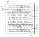
도 3은 본 발명에 따른 발광 소자 유닛의 일 예를 도시한 것으로, 7×7 배열 구조를 갖는다. 서브 마운트(100)에 전기 배선(130)이 형성되어 있고, 상기 전기 배선(130)에 따라 제1 및 제2 발광 소자들(112)(122)이 실장된다. 도면에서는 편의상 발광 소자들의 전극 구조만을 도시하였다.3 illustrates an example of a light emitting device unit according to the present invention, and has a 7 × 7 arrangement. An
제1 발광 소자들(112)이 직렬로 연결되고, 제2 발광 소자들(122)이 브릿지 형태로 배열되어 있다. 상기 제2 발광 소자들(122)은 브릿지 회로의 한 변에 7개씩 직렬로 연결되어 있다. 제2 발광 소자를 7개로 구성하는 것은 일 예에 불과하며, 제2 발광 소자 들 중의 한 소자에 걸리는 역방향 전압이 브레이크 다운 전압(Vb) 보다 작은 한도 내에서 제2 발광 소자의 개수를 다양하게 구성할 수 있다.The first
상기 제2 발광 소자(122)는 브레이크 다운 전압(Vb)이 다음의 수학식을 만족하도록 구성되는 것이 좋다.The second

여기서, Vf는 제2 발광 소자의 순방향 전압을, Vp는 공급 전압의 최대값을, n은 브릿지 회로의 한 변에 배열되는 제2 발광 소자의 개수를 나타낸다. 다시 말하면, 제2 발광 소자(122)의 브레이크 다운 전압(Vb)은 역방향 전압보다 커야 한다. 예를 들어, Vp=110(V)이고, n=7이고, vf=3.5(V) 일 때, Vb는 12(V)보다 큰 값을 가지는 것이 좋다. 제2 발광 소자의 역방향 전압이 상기 수학식 1을 만족시키는 범위 내에서 제2 발광 소자의 개수(n)를 정할 수 있다.Here, Vf represents the forward voltage of the second light emitting device, Vp represents the maximum value of the supply voltage, and n represents the number of second light emitting devices arranged on one side of the bridge circuit. In other words, the breakdown voltage Vb of the second
다음, 도 4a 및 도 4b를 참조하여 발광 소자 유닛의 발광 동작에 대해 설명하기로 한다.Next, the light emission operation of the light emitting device unit will be described with reference to FIGS. 4A and 4B.
도 4a는 전원(105)으로부터의 교류 전압의 순방향의 제1 반주기 동안의 전류의 흐름을, 도 4b는 역방향의 제2 반주기 동안의 전류의 흐름을 나타낸 것이다. 제1 반주기 동안에는 제1변(120a)의 제2 발광소자들, 제1 발광소자들(112), 제3변(120c)의 제2 발광소자들을 통해 전류가 흐른다. 한편, 제2 반주기 동안에는 제2변(120c)의 제2 발광소자들, 제1 발광소자들(112), 제4변(120d)의 제2 발광소자들을 통해 전류가 흐른다. 결과적으로, 제2 발광소자들은 전체 개수의 절반씩 교대로 발광되는 한편, 제1 발광소자들은 연속적으로 발광된다. 제2 발광 소자들은 정류 작용과 발광 작용을 같이 하게 된다. 따라서, 기존에 병렬 구조의 발광 소자에 비해 발광 효율이 향상된다. 본 발명의 발광 소자 유닛에서 교류 전압의 절반의 주기 동안 발광이 되는 제1 및 제2 발광 소자의 개수는 (Vp/Vf) 보다 크다.4A shows the flow of current during the first half period in the forward direction of the alternating voltage from the
한편, 상기 제1 및 제2 발광 소자(112)(122)는 상기 서브 마운트에 플립칩으로 실장될 수 있다. 발광 소자를 와이어 없이 플립칩으로 실장함으로써 제조 공정을 단순화함과 아울러 발광 소자와 발광 소자 사이의 간격을 줄일 수 있어 소형화에 도움이 된다.The first and second
도 5는 발광 소자의 일예를 도시한 것으로, 사파이어 기판(227) 상에 전자가 도핑된 n형 클래드층(225), 활성층(224), 정공이 도핑된 p형 클래드층(223) 및 p형 전극(221)이 차례대로 적층되어 있다. 그리고, 상기 n형 클래드층(225)의 일측 하부면에 n형 전극(226)이 구비된다. 상기 n형 클래드층(225)이 단차지게 형성되고, 그 단차 진 부분에 n형 전극(226)이 구비된다.FIG. 5 illustrates an example of a light emitting device, and includes an n-
상기 제p형 전극 및 n형 전극(221)(226)에 각각 플러스와 마이너스 전압을 순방향으로 가하면 상기 p형 및 n형 클래드층(223)(225)에서 상기 활성층(224)으로 전자와 정공이 이동되고, 이 전자와 정공의 결합을 통하여 에너지 밴드 갭에 해당하는 에너지를 갖는 광자가 발생되어 발광된다. 상기와 같이 구성된 발광 소자를 서브 마운트(220)의 배선에 따라 배치하여 플립칩으로 실장함으로써 간단하게 발광 소자 유닛을 제작할 수 있다. 도면 부호 230은 본딩 메탈을 나타낸다. 이 밖에 p형 전극 및 n형 전극이 서로 반대 방향의 면에 배치되는 구조의 발광 소자를 이용하여 발광 소자 유닛을 제작하는 것도 가능하다.When positive and negative voltages are applied to the p-type electrode and the n-
본 발명에서는 발광 소자를 브릿지 형태로 배열함으로써 정류 작용과 함께 발광 작용을 하도록 함으로써 발광 소자 유닛의 발광 효율을 높임과 아울러 소형화에 기여할 수 있다.In the present invention, by arranging the light emitting elements in the form of a bridge, the light emitting action is performed together with the rectifying action, thereby increasing the light emitting efficiency of the light emitting element unit and contributing to miniaturization.
상술한 바와 같이 본 발명에 따른 발광 소자 유닛은, 발광 소자들을 브릿지 회로 및 직렬로 연결하여 별도의 정류 소자 없이 브릿지 회로를 통해 정류 동작을 하도록 함으로써 구조를 단순화 및 소형화할 수 있다. 또한, 브릿지 회로를 통한 정류 동작에 의해 일반적인 직렬 및 병렬 배열에 비해 발광 효율을 향상시킬 수 있다. 또한, 정류 소자를 별도로 제작할 필요 없이 발광 소자들의 배열만으로 정류 작용을 구현함으로써 비용이 절감되는 효과가 있다. 이와 같이 발광 소자 유닛의 소형화 및 고휘도화를 통해 교류 전압의 조명 광원에 유용하게 적용될 수 있다.As described above, the light emitting device unit according to the present invention can simplify and downsize the structure by connecting the light emitting devices in series with the bridge circuit to perform rectifying operation through the bridge circuit without a separate rectifying device. In addition, by the rectifying operation through the bridge circuit it is possible to improve the luminous efficiency compared to the general series and parallel arrangement. In addition, there is an effect that the cost is reduced by implementing the rectifying action only by the arrangement of the light emitting elements without having to manufacture a separate rectifying device. As such, the light emitting device unit may be usefully applied to an illuminating light source of an AC voltage through miniaturization and high brightness.
상기한 실시예 들은 예시적인 것에 불과한 것으로, 당해 기술분야의 통상을 지식을 가진 자라면 이로부터 다양한 변형 및 균등한 타 실시예가 가능하다. 따라서, 본 발명의 진정한 기술적 보호범위는 하기의 특허청구범위에 기재된 발명의 기술적 사상에 의해 정해져야만 할 것이다.The above embodiments are merely exemplary, and various modifications and equivalent other embodiments are possible to those skilled in the art. Therefore, the true technical protection scope of the present invention will be defined by the technical spirit of the invention described in the claims below.
Claims (6)
Translated fromKorean
Priority Applications (3)
| Application Number | Priority Date | Filing Date | Title |
|---|---|---|---|
| KR1020060025212AKR20070095041A (en) | 2006-03-20 | 2006-03-20 | Light-emitting element unit for AC voltage |
| US11/655,830US20070217210A1 (en) | 2006-03-20 | 2007-01-22 | Light emitting device unit for AC voltage |
| JP2007035259AJP4989251B2 (en) | 2006-03-20 | 2007-02-15 | Light-emitting element unit for AC voltage |
Applications Claiming Priority (1)
| Application Number | Priority Date | Filing Date | Title |
|---|---|---|---|
| KR1020060025212AKR20070095041A (en) | 2006-03-20 | 2006-03-20 | Light-emitting element unit for AC voltage |
Publications (1)
| Publication Number | Publication Date |
|---|---|
| KR20070095041Atrue KR20070095041A (en) | 2007-09-28 |
Family
ID=38517624
Family Applications (1)
| Application Number | Title | Priority Date | Filing Date |
|---|---|---|---|
| KR1020060025212ACeasedKR20070095041A (en) | 2006-03-20 | 2006-03-20 | Light-emitting element unit for AC voltage |
Country Status (3)
| Country | Link |
|---|---|
| US (1) | US20070217210A1 (en) |
| JP (1) | JP4989251B2 (en) |
| KR (1) | KR20070095041A (en) |
Cited By (1)
| Publication number | Priority date | Publication date | Assignee | Title |
|---|---|---|---|---|
| KR101523002B1 (en)* | 2009-01-13 | 2015-05-26 | 서울반도체 주식회사 | Light emitting device |
Families Citing this family (12)
| Publication number | Priority date | Publication date | Assignee | Title |
|---|---|---|---|---|
| TW200704283A (en) | 2005-05-27 | 2007-01-16 | Lamina Ceramics Inc | Solid state LED bridge rectifier light engine |
| US7863825B2 (en)* | 2007-01-30 | 2011-01-04 | Addtek Corp. | LED driver circuit for providing desired luminance with constant current |
| TWI369777B (en)* | 2007-10-04 | 2012-08-01 | Young Lighting Technology Corp | Surface light source of backlight module in a flat panel display |
| TWI416993B (en)* | 2008-05-21 | 2013-11-21 | Interlight Optotech Corp | Alternate current light emitting diode module and light source apparatus using the same and manufacturing method thereof |
| KR101495071B1 (en)* | 2008-06-24 | 2015-02-25 | 삼성전자 주식회사 | Sub-mount, light emitting device using the same and fabricating method of sub-mount, fabricating method of light emitting device using the same |
| KR101448153B1 (en)* | 2008-06-25 | 2014-10-08 | 삼성전자주식회사 | A multi-chip package for a light-emitting diode and a light-emitting diode |
| KR101025972B1 (en)* | 2008-06-30 | 2011-03-30 | 삼성엘이디 주식회사 | AC drive light emitting device |
| US8752980B2 (en)* | 2009-05-27 | 2014-06-17 | Hong-Yuan Technology Co., Ltd. | Illumination system and method of manufacturing multi-chip package structure for light emitting diodes |
| US8760058B2 (en) | 2012-02-02 | 2014-06-24 | Posco Led Company Ltd. | Heat sink and LED illuminating apparatus comprising the same |
| CN103388805B (en)* | 2013-07-01 | 2015-03-18 | 临安市新三联照明电器有限公司 | LED (Light Emitting Diode) filament support series connection forming method based on support material plate |
| FR3061625B1 (en)* | 2016-12-30 | 2020-07-24 | Commissariat Energie Atomique | ELECTRONIC STRUCTURE INCLUDING A MATRIX OF ELECTRONIC DEVICES PRESENTING IMPROVED THERMAL PERFORMANCES |
| KR102777054B1 (en)* | 2019-07-04 | 2025-03-11 | 서울반도체 주식회사 | Light emitting module having plurality of light emitting diode chip connected in seires-parallel |
Family Cites Families (11)
| Publication number | Priority date | Publication date | Assignee | Title |
|---|---|---|---|---|
| JPS6364059U (en)* | 1986-10-14 | 1988-04-27 | ||
| KR100520721B1 (en)* | 1999-12-14 | 2005-10-11 | 가부시키가이샤 다키온 | Power supply and led lamp device |
| DE10054212A1 (en)* | 2000-11-02 | 2002-05-08 | Hans Dokoupil | Night-light for mains sockets, especially wall sockets has ballast with current-limiting condenser, voltage-stable with small dimensions and at least one lamp element as lighting device |
| AU2003272821A1 (en)* | 2002-10-01 | 2004-04-23 | Sloanled, Inc. | Bent perimeter lighting and method for fabricating |
| US6982518B2 (en)* | 2003-10-01 | 2006-01-03 | Enertron, Inc. | Methods and apparatus for an LED light |
| JP4841550B2 (en)* | 2004-06-30 | 2011-12-21 | ソウル オプト デバイス カンパニー リミテッド | LIGHT EMITTING ELEMENT, ITS MANUFACTURING METHOD, AND LIGHT EMITTING DEVICE USING THE SAME |
| JP4337731B2 (en)* | 2004-12-22 | 2009-09-30 | ソニー株式会社 | Illumination device and image display device |
| US7138770B2 (en)* | 2004-12-27 | 2006-11-21 | Top Union Globaltek Inc. | LED driving circuit |
| TW200640045A (en)* | 2005-05-13 | 2006-11-16 | Ind Tech Res Inst | Alternating current light-emitting device |
| US7948770B2 (en)* | 2005-12-09 | 2011-05-24 | Industrial Technology Research Institute | AC—LED system in single chip with three metal contacts |
| US7148515B1 (en)* | 2006-01-07 | 2006-12-12 | Tyntek Corp. | Light emitting device having integrated rectifier circuit in substrate |
- 2006
- 2006-03-20KRKR1020060025212Apatent/KR20070095041A/ennot_activeCeased
- 2007
- 2007-01-22USUS11/655,830patent/US20070217210A1/ennot_activeAbandoned
- 2007-02-15JPJP2007035259Apatent/JP4989251B2/ennot_activeExpired - Fee Related
Cited By (1)
| Publication number | Priority date | Publication date | Assignee | Title |
|---|---|---|---|---|
| KR101523002B1 (en)* | 2009-01-13 | 2015-05-26 | 서울반도체 주식회사 | Light emitting device |
Also Published As
| Publication number | Publication date |
|---|---|
| JP2007258690A (en) | 2007-10-04 |
| JP4989251B2 (en) | 2012-08-01 |
| US20070217210A1 (en) | 2007-09-20 |
Similar Documents
| Publication | Publication Date | Title |
|---|---|---|
| KR20070095041A (en) | Light-emitting element unit for AC voltage | |
| KR101239853B1 (en) | Ac light emitting diode | |
| EP2445018B1 (en) | Semiconductor light-emitting device, light-emitting module, and illumination device | |
| US20080218093A1 (en) | Structure of AC light-emitting diode dies | |
| WO2013136389A1 (en) | Substrate, light-emitting device, and illumination device | |
| US8766536B2 (en) | Light-emitting module having light-emitting elements sealed with sealing member and luminaire having same | |
| KR20100028461A (en) | Alternating current light emitting device | |
| KR101783955B1 (en) | Light emitting diode package and back light unit having the same | |
| RU2456704C1 (en) | Lighting device | |
| CN108140696A (en) | Micro wire containing temperature measuring equipment or nanowire LED light source | |
| TW201618275A (en) | Light-emitting diode | |
| KR20060084315A (en) | LED array circuit | |
| US8558249B1 (en) | Rectifier structures for AC LED systems | |
| JP2014150292A (en) | Light-emitting device | |
| TWI473294B (en) | Light-emitting apparatus | |
| KR20100038252A (en) | White light emitting diode package | |
| KR100690321B1 (en) | Light emitting diode having light emitting cell arrays and method of manufacturing same | |
| US9345086B2 (en) | Lighting circuit | |
| KR101121714B1 (en) | Luminous Device | |
| KR200483284Y1 (en) | LED module structure of LED tubular light | |
| JP2006319290A (en) | Light emitting diode light source unit and valve type thereof | |
| KR101001242B1 (en) | AC LED | |
| KR100965243B1 (en) | AC LED | |
| CN111341199B (en) | Light source assembly, method for reducing working current of backlight module and display device | |
| KR100990423B1 (en) | LED module in surface mount element type |
Legal Events
| Date | Code | Title | Description |
|---|---|---|---|
| PA0109 | Patent application | Patent event code:PA01091R01D Comment text:Patent Application Patent event date:20060320 | |
| A201 | Request for examination | ||
| PA0201 | Request for examination | Patent event code:PA02012R01D Patent event date:20070509 Comment text:Request for Examination of Application Patent event code:PA02011R01I Patent event date:20060320 Comment text:Patent Application | |
| PG1501 | Laying open of application | ||
| E902 | Notification of reason for refusal | ||
| PE0902 | Notice of grounds for rejection | Comment text:Notification of reason for refusal Patent event date:20080410 Patent event code:PE09021S01D | |
| E601 | Decision to refuse application | ||
| PE0601 | Decision on rejection of patent | Patent event date:20081027 Comment text:Decision to Refuse Application Patent event code:PE06012S01D Patent event date:20080410 Comment text:Notification of reason for refusal Patent event code:PE06011S01I |