KR20070094022A - Pointing device - Google Patents
Pointing deviceDownload PDFInfo
- Publication number
- KR20070094022A KR20070094022AKR1020077017775AKR20077017775AKR20070094022AKR 20070094022 AKR20070094022 AKR 20070094022AKR 1020077017775 AKR1020077017775 AKR 1020077017775AKR 20077017775 AKR20077017775 AKR 20077017775AKR 20070094022 AKR20070094022 AKR 20070094022A
- Authority
- KR
- South Korea
- Prior art keywords
- ring
- magnet
- magnetic sensor
- magnetic
- pointing device
- Prior art date
- Legal status (The legal status is an assumption and is not a legal conclusion. Google has not performed a legal analysis and makes no representation as to the accuracy of the status listed.)
- Granted
Links
Images


Classifications
- G—PHYSICS
- G06—COMPUTING OR CALCULATING; COUNTING
- G06F—ELECTRIC DIGITAL DATA PROCESSING
- G06F3/00—Input arrangements for transferring data to be processed into a form capable of being handled by the computer; Output arrangements for transferring data from processing unit to output unit, e.g. interface arrangements
- G06F3/01—Input arrangements or combined input and output arrangements for interaction between user and computer
- G06F3/03—Arrangements for converting the position or the displacement of a member into a coded form
- G06F3/033—Pointing devices displaced or positioned by the user, e.g. mice, trackballs, pens or joysticks; Accessories therefor
- G06F3/0338—Pointing devices displaced or positioned by the user, e.g. mice, trackballs, pens or joysticks; Accessories therefor with detection of limited linear or angular displacement of an operating part of the device from a neutral position, e.g. isotonic or isometric joysticks
- G—PHYSICS
- G06—COMPUTING OR CALCULATING; COUNTING
- G06F—ELECTRIC DIGITAL DATA PROCESSING
- G06F3/00—Input arrangements for transferring data to be processed into a form capable of being handled by the computer; Output arrangements for transferring data from processing unit to output unit, e.g. interface arrangements
- G06F3/01—Input arrangements or combined input and output arrangements for interaction between user and computer
- G06F3/03—Arrangements for converting the position or the displacement of a member into a coded form
- G06F3/033—Pointing devices displaced or positioned by the user, e.g. mice, trackballs, pens or joysticks; Accessories therefor
- G06F3/0354—Pointing devices displaced or positioned by the user, e.g. mice, trackballs, pens or joysticks; Accessories therefor with detection of 2D relative movements between the device, or an operating part thereof, and a plane or surface, e.g. 2D mice, trackballs, pens or pucks
Landscapes
- Engineering & Computer Science (AREA)
- General Engineering & Computer Science (AREA)
- Theoretical Computer Science (AREA)
- Human Computer Interaction (AREA)
- Physics & Mathematics (AREA)
- General Physics & Mathematics (AREA)
- Position Input By Displaying (AREA)
- Measuring Magnetic Variables (AREA)
- Switches With Compound Operations (AREA)
- Switches That Are Operated By Magnetic Or Electric Fields (AREA)
Abstract
Translated fromKoreanDescription
Translated fromKorean본 발명은 퍼스널 컴퓨터나 휴대 전화 등의 입력 수단으로서 사용되는 포인팅 디바이스에 관한 것으로, 보다 상세하게는 마그넷의 이동에 의한 주위의 자속 밀도 변화를 검출함으로써 좌표 검지 또는 벡터 정보를 입력하기 위한 자기 검출 방식의 포인팅 디바이스에 관한 것이다.BACKGROUND OF THE
도1은 종래의 자기 검출식 포인팅 디바이스의 자기 검출 회로를 나타내는 블록도로, 검출부(1)는 4개의 자기 센서(예를 들어, 홀 소자, 반도체 자기 저항 효과 소자, 자성 박막 자기 저항 효과 소자, GMR 소자)(11)로 이루어지고, 이 홀 소자(11)는 X축 및 Y축을 따라서 2개씩 대칭으로 배치되어 있다. X축 및 Y축 상에 대칭으로 배치된 4개의 홀 소자(11)의 중앙 부근에 마그넷이 배치되어 있다. 이 마그넷의 이동에 의한 자속 밀도의 변화에 의해 홀 소자(11)의 출력 전압이 변화한다.FIG. 1 is a block diagram showing a magnetic detection circuit of a conventional magnetic detection type pointing device. The
차동 증폭기(2)는 X축 방향과 Y축 방향의 각 홀 소자(11)의 출력을 각각 차동적으로 증폭한다. Z축 방향의 자속 밀도가 원점(O)에 대해 대칭, 즉 마그넷의 착자 방향이 수직 방향에 있을 때, 출력이 0이 되도록 되어 있고, 마그넷이 이동하 면, 이에 따라서 차동 증폭기(2)에 출력이 발생하여 그 출력(아날로그치)을 검출 제어부(3)가 X 좌표치 및 Y 좌표치로 변환하여, 이를 출력 제어부(4)가 출력하도록 구성되어 있다.The
휴대 전화 등에 이용되는 소형의 포인팅 디바이스의 구체예로서는, 키매트에 자석을 배치하는 방법을 채용한 것이 있다. 이 방법의 것은, 현재 제안되어 있는 것 중에서는 소형화가 가능한 것이다(예를 들어, 일본 특허 공개 제2002-150904호 공보 참조).As a specific example of a small pointing device used in a portable telephone or the like, there is a method in which a magnet is disposed on a key mat. This method is capable of miniaturization among those currently proposed (see, for example, Japanese Patent Application Laid-Open No. 2002-150904).
접촉식 포인팅 디바이스로서는, 기판 상에 빗살 형상의 2세트의 전극을 형성해 놓고, 그 상부로부터 도전성 고무를 압박함으로써 통전 상태를 변화시켜 디지털치로서 좌표치를 출력하는 것이 일반적이다.As the contact type pointing device, two sets of electrodes in the form of comb teeth are formed on a substrate, and the conductive state is changed from the upper portion by pressing the conductive rubber to output a coordinate value as a digital value.
그러나, 휴대 전화 등의 소형의 휴대 전자 기기에 있어서는, 전자 기기의 전체 사이즈를 작게 하고, 또한 기능을 향상시키는 서로 모순되는 필요성을 충족시키기 위해 한층 부품의 소형화나 저등화가 요구되고 있다. 또한, 자기 검출식 포인팅 디바이스의 한층 조작감의 향상도 기대되고 있다.However, in a small portable electronic device such as a cellular phone, the miniaturization and lowering of parts are required to meet the contradictory necessity of reducing the overall size of the electronic device and improving the function. In addition, improvement in operation feeling of the magnetic detection type pointing device is expected.
또한, 상술한 공보의 예에서는 마그넷을 수직 방향으로 착자하고 있으므로, 외부로 누설되는 자속 밀도가 커져 근처에 자기 카드를 근접시킨 경우, 이 자기 카드 등의 정보를 소실하게 되는 문제가 위구되고 있다.In addition, in the above-mentioned publication, since the magnet is magnetized in the vertical direction, when the magnetic flux density leaking to the outside becomes large and the magnetic card is brought close to the outside, the problem of losing information of the magnetic card or the like can be achieved.
또한, 접촉식 포인팅 디바이스에 있어서는, 도전성 고무를 압박하여 입력하고 있으므로, 반복 입력 등에 의해 도전성 고무의 열화를 피할 수 없어 수명이 짧아지는 문제가 발생하고 있다.Further, in the contact type pointing device, since the conductive rubber is pressed and input, deterioration of the conductive rubber can not be avoided due to repetitive input or the like, resulting in a problem that the service life is shortened.
본 발명은 이와 같은 문제에 비추어 이루어진 것으로, 그 목적으로 하는 바는, 소형화와 저등화가 가능하며 조작감이 양호하고, 또한 외부로의 누설 자속 밀도가 작고, 또는 제품 수명이 긴 포인팅 디바이스를 제공하는 데 있다.An object of the present invention is to provide a pointing device capable of downsizing and downsizing, having a good operation feeling, a small leakage magnetic flux density to the outside, or a long product life have.
본 발명은 이와 같은 목적을 달성하기 위해, 평면에 대해 평행하게 이동 가능하게 지지된 링형 자석과, 상기 링형 자석이 발생하는 상기 평면과 평행한 방향의 자속 밀도를 검지하는 복수의 자기 센서를 구비하고, 상기 링형 자석의 이동에 의해 발생하는 상기 평면과 평행한 방향의 자속 밀도의 변화를 상기 자기 센서로 검출하는 것을 특징으로 하는 것이다.In order to achieve the above object, the present invention provides a magnetic bearing device comprising: a ring-shaped magnet supported movably in parallel with a plane; and a plurality of magnetic sensors for detecting a magnetic flux density in a direction parallel to the plane in which the ring- And the magnetic sensor detects a change in the magnetic flux density in a direction parallel to the plane generated by the movement of the ring-like magnet.
또한, 상기 링형 자석은 내외 단극 착자되어 있는 것을 특징으로 하는 것이다.Further, the ring-shaped magnet is characterized in that it is internally and externally unipolarly magnetized.
또한, 상기 링형 자석은 내주부 혹은 외주부 중 적어도 한쪽이 다극 착자되어 있고, 상기 자기 센서는 상기 다극 착자된 링형 자석의 자극 중심에 대향하고 있는 것을 특징으로 하는 것이다.Further, the ring-shaped magnet is characterized in that at least one of the inner circumferential portion and the outer circumferential portion is multipolar-magnetized, and the magnetic sensor is opposed to the magnetic pole center of the multipolar magnetized magnet.
또한, 실장 기판 상에 수지층이 설치되고, 상기 수지층에 상기 링형 자석이 고정 부착되는 동시에, 상기 실장 기판 상에 상기 자기 센서를 배치한 것을 특징으로 하는 것이다.Further, a resin layer is provided on a mounting substrate, the ring-shaped magnet is fixedly attached to the resin layer, and the magnetic sensor is disposed on the mounting substrate.
또한, 상기 수지층과 상기 실장 기판과의 대향면이 접착되어 있지 않은 것을 특징으로 하는 것이다.In addition, the resin layer and the mounting substrate are not bonded to each other.
또한, 상기 수지층은 탄성 시트인 것을 특징으로 하는 것이다.Further, the resin layer is an elastic sheet.
또한, 상기 수지층이 실리콘 수지인 것을 특징으로 하는 것이다.Further, the resin layer is a silicone resin.
또한, 상기 자기 센서는 직교계의 2차원 평면 상의 2축인 X축 및 Y축에 따라서 대칭으로 배치되고, 상기 링형 자석은 상기 자기 센서의 중앙 부근에 배치되어 있는 것을 특징으로 하는 것이다.The magnetic sensor is symmetrically arranged along the X axis and the Y axis which are two axes on the two-dimensional plane of the serial system, and the ring-shaped magnet is disposed near the center of the magnetic sensor.
또한, 상기 실장 기판의 상기 수지층측이고, 또한 상기 링형 자석의 대략 중앙 부분에 스위치를 배치한 것을 특징으로 하는 것이다.Further, a switch is disposed on the side of the resin layer of the mounting board, and the switch is disposed at a substantially central portion of the ring-shaped magnet.
또한, 상기 스위치에 대향하는 상기 수지층의 부분에 상기 스위치를 압박하기 위한 돌기를 마련한 것을 특징으로 하는 것이다.Further, a protrusion for pressing the switch is provided on a portion of the resin layer opposed to the switch.
또한, 상기 자기 센서는 홀 효과를 이용한 자기 센서로, 자속 밀도에 비례한 신호를 출력하는 것을 특징으로 하는 것이다.The magnetic sensor is a magnetic sensor using a Hall effect, and outputs a signal proportional to the magnetic flux density.
또한, 상기 홀 효과를 이용한 자기 센서가 상기 실장 기판의 상기 수지층측에 배치되고, 또한 상기 실장 기판의 표면에 평행한 방향의 자속 밀도를 검출하도록 설치되어 있는 것을 특징으로 하는 것이다.A magnetic sensor using the Hall effect is disposed on the resin layer side of the mounting board and is arranged to detect a magnetic flux density in a direction parallel to the surface of the mounting board.
또한, 상기 홀 효과를 이용한 자기 센서가 출력 단자를 1개만 갖는 자기 센서인 것을 특징으로 하는 것이다.Further, the magnetic sensor using the hall effect is a magnetic sensor having only one output terminal.
또한, 상기 자기 센서가 자기 저항 효과를 이용한 자기 센서인 것을 특징으로 하는 것이다.Further, the magnetic sensor is a magnetic sensor using a magneto-resistive effect.
또한, 상기 자기 저항 효과를 이용한 자기 센서는 반도체 자기 저항 효과 소 자로, 상기 실장 기판의 상기 수지층측에 배치되고, 또한 상기 실장 기판의 표면에 평행한 방향의 자속 밀도를 검출하는 것을 특징으로 하는 것이다.The magnetic sensor using the magnetoresistive effect is characterized in that the magnetic flux density in the direction parallel to the surface of the mounting substrate is detected on the side of the resin layer of the mounting substrate in a semiconductor magnetoresistance effect element will be.
또한, 상기 자기 저항 효과를 이용한 자기 센서는 4개의 반도체 자기 저항 효과 소자로, 직교계의 2차원 평면 상의 2축인 X축 및 Y축을 따라서 2개씩 대칭으로 배치되어, 상기 X축 상의 2개의 자기 센서는 제1 결합점에서 전기적으로 결합되고, 상기 Y축 상의 2개의 자기 센서도 제2 결합점에서 전기적으로 결합되어 있고, 상기 제1 및 제2 결합점에서의 전기 신호를 이용하여 상기 링형 자석의 이동에 의해 생기는 주위의 자속 밀도의 변화를 검지하는 것을 특징으로 하는 것이다.The magnetic sensor using the magnetoresistive effect is composed of four semiconductor magnetoresistance effect elements, which are symmetrically arranged two by two along the X axis and the Y axis, which are two axes on the two-dimensional plane of the direct current system, And the two magnetic sensors on the Y axis are also electrically coupled to each other at a second coupling point, and the electric signals at the first and second coupling points are used to electrically connect the ring- And detects a change in the magnetic flux density around the magnetic pole caused by the movement.
또한, 상기 링형 자석으로부터 발생되는 자력을 이용하여 상기 링형 자석을 원점으로 복귀시키는 원점 복귀 수단을 갖는 것을 특징으로 하는 것이다.And an origin returning means for returning the ring-like magnet to the origin by using the magnetic force generated from the ring-shaped magnet.
또한, 상술한 포인팅 디바이스가 조립된 것을 특징으로 하는 전자 장치이다.Further, the electronic device is characterized in that the above-described pointing device is assembled.
자기 센서로서는, 홀 소자, 홀 IC, 자기 저항 효과 소자(MR 소자), 자기 저항 효과 IC(MRIC), 리드 스위치 등 다양한 자기 센서의 적용이 가능하고, 아날로그 출력형의 포인팅 디바이스에는 아날로그 출력형의 자기 센서가 바람직하고, 디지털 출력형의 포인팅 디바이스에는 디지털 출력형의 자기 센서가 바람직하다.As the magnetic sensor, various magnetic sensors such as a Hall element, a Hall IC, a magnetoresistance effect element (MR element), a magnetoresistive effect IC (MRIC), and a reed switch can be applied. In the analog output type pointing device, A magnetic sensor is preferable, and a digital output type magnetic sensor is preferable for a digital output type pointing device.
홀 소자를 이용하는 경우, 실장 기판의 수지층측에 배치하고, 또한 실장 기판 표면에 평행한 방향의 자속 밀도를 검출하도록 하는 것이 포인팅 디바이스의 소형화와 저등화를 진행시키는 데 있어서 한층 바람직하다.It is more preferable to arrange the Hall element on the resin layer side of the mounting board and to detect the magnetic flux density in the direction parallel to the surface of the mounting board in order to advance the downsizing and the lowering of the pointing device.
홀 효과를 이용한 자기 센서가 홀 IC이고, 출력 단자를 1개만을 갖는 자기 센서이면, 출력 신호선의 수를 홀 소자에 비해 저감시킬 수 있으므로, 실장 기판의 공간 절약화와 외부 노이즈의 영향의 저감을 도모할 수 있다.The number of output signal lines can be reduced as compared with the case of a Hall element in the case of a magnetic sensor using a Hall effect and a magnetic sensor having only one output terminal so that the space saving of the mounting board and the influence of external noise can be reduced .
자기 저항 효과를 이용한 자기 센서를 이용하는 경우에는 반도체 자기 저항 효과 소자를 이용하여 실장 기판의 수지층측에 배치하고, 또한 실장 기판 표면에 평행한 방향의 자속 밀도를 검출하도록 하는 것이 포인팅 디바이스의 소형화와 저등화를 진행시키는 데 있어서 한층 바람직하다.In the case of using a magnetic sensor using a magneto-resistive effect, it is preferable to arrange the magneto-resistive effect element on the resin layer side of the mounting board by using a semiconductor magneto-resistance effect element and to detect the magnetic flux density in a direction parallel to the surface of the mounting board. And it is more preferable for advancing the low equalization.
또한, 4개의 반도체 자기 저항 효과 소자를 직교계의 2차원 평면 상의 2축인 X축 및 Y축을 따라서 2개씩 대칭으로 배치하여, X축 상의 2개의 반도체 자기 저항 효과 소자를 제1 결합점에서 전기적으로 결합하고, Y축 상의 2개의 반도체 자기 저항 효과 소자도 제2 결합점에서 전기적으로 결합하고, 제1 및 제2 결합점에 있어서의 전기 신호를 이용하여 링형 자석의 이동에 의해 발생하는 주위의 자속 밀도의 변화를 검지하도록 해도 좋다. 이와 같은 구성을 취함으로써, 홀 소자를 이용하는 경우에 비해 출력 신호선의 수를 저감시킬 수 있으므로, 실장 기판의 공간 절약화와 외부 노이즈의 영향의 저감을 도모할 수 있다.Four semiconductor magnetoresistance effect elements are symmetrically arranged two by two along the X axis and the Y axis, which are two axes on the two-dimensional plane of the direct current system, and two semiconductor magnetoresistance effect elements on the X axis are electrically And two semiconductor magnetoresistive effect elements on the Y axis are electrically coupled to each other at a second coupling point, and the peripheral magnetic flux generated by the movement of the ring-like magnet using the electric signals at the first and second coupling points A change in the density may be detected. By adopting such a configuration, the number of output signal lines can be reduced as compared with the case of using a Hall element, so that space saving of the mounting board and reduction of the influence of external noise can be achieved.
또한, 실장 기판의 수지층측에 스위치를 배치해도 좋다. 또한, 스위치에 대향하는 수지층 부분에 스위치를 누르기 위한 돌기를 마련해도 좋다. 스위치로서는, 특별히 종류의 한정은 없지만, 누른 것을 확인하기 쉽고(클릭감이 있음), 스위치를 압입한 후에 자동 복귀하는 택틸(tactile) 스위치, 누름 버튼 스위치, 택트(tact) 스위치, 터치(touch) 스위치, 스트로크(stroke) 스위치 등 대상물과의 물리적 접촉을 이용하여 대상물을 확인하는 스위치가 적합하고, 택틸 스위치(돔 스위치라고도 함)가 소형화나 저등화를 진행시키는 데 있어서 바람직하다.A switch may be disposed on the resin layer side of the mounting substrate. A protrusion for pressing the switch may be provided on the resin layer portion opposed to the switch. The tactile switch, the push button switch, the tact switch, the touch switch, and the like, which are easy to confirm the click (there is a sense of clicking), automatically return after pushing the switch, A switch for confirming an object using a physical contact with an object such as a switch or a stroke switch is suitable, and a tactile switch (also referred to as a dome switch) is preferable for advancing miniaturization and low-equalization.
또한, 링형 자석에 대해서도 특별히 종류의 한정은 없지만, 통상 양산되어 있는 페라이트계, 사마륨-코발트계, 네오디계 등 다양한 링형 자석이 적용 가능하다. 포인팅 디바이스의 소형화를 진행키는 데 있어서는 마그넷의 소형화가 필수이므로, 작더라도 강자장을 발생하는 사마륨-코발트계나 네오디계 등의 링형 자석이 바람직하다. 또한, 자석의 저등화를 진행시키는 데 있어서는, 벌크 자석보다 성형성이 좋은 본드 자석이 바람직하다. 형상에 대해서는, 같은 착자를 하면 링형에 한정되지 않고, 원기둥 형상이나 각기둥 형상 등이라도 당연히 좋다. 단, 링형 자석을 이용함으로써 실장 기판에 스위치를 배치해도, 포인팅 디바이스 전체의 높이를 억제하는 것이 가능해지므로 더욱 바람직하다.There is no particular limitation on the ring type magnet, but various ring type magnets such as a ferrite type, samarium-cobalt type, and neodymium type which are usually mass-produced are applicable. In order to promote downsizing of the pointing device, it is necessary to downsize the magnet, so that a ring-shaped magnet such as a samarium-cobalt or neodymium which generates a strong magnetic field is preferable. Further, in order to promote the lowering of the magnet, a bonded magnet having better moldability than the bulk magnet is preferable. Regarding the shape, it is not limited to a ring shape if the same ring is formed, and a cylindrical shape or a prism shape is of course preferable. However, even if a switch is arranged on the mounting substrate by using the ring-shaped magnet, the entire height of the pointing device can be suppressed, which is more preferable.
수지층은 탄력성을 갖는 수지가 바람직하고, 탄력성을 갖는 수지에 대해서도 특별히 종류의 한정은 없지만, 현재 다양한 용도로 사용되고 있는 실리콘 수지가 저렴하고 입수하기 쉬우므로 바람직하다.The resin layer is preferably a resin having elasticity, and a resin having elasticity is not particularly limited, but a silicone resin which is currently used for various purposes is preferable because it is inexpensive and easy to obtain.
또한, 링형 자석은 실장 기판의 표면에 대해 대략 평행 이동함으로써 주위의 자속 밀도 변화를 생기게 하면, 포인팅 디바이스의 보다 한층 저등화가 가능해지므로 바람직하다.In addition, it is preferable that the ring-like magnet is moved approximately parallel to the surface of the mounting substrate to cause a change in the magnetic flux density around the ring-shaped magnet, because further lowering of the pointing device becomes possible.
또한, 수지층과 실장 기판의 대향면이 접착되어 있지 않은 것이 바람직하다.In addition, it is preferable that the resin layer and the mounting substrate are not bonded to each other.
또한, 자기 센서는 직교계의 2차원 평면 상의 2축인 X축 및 Y축에 따라서 대칭으로 배치되고, 링형 자석은 자기 센서의 중앙 부근에 배치되어 있는 것이 바람직하다.It is also preferable that the magnetic sensors are arranged symmetrically with respect to the X axis and the Y axis, which are two axes on the two-dimensional plane of the serial system, and the ring-shaped magnets are disposed near the center of the magnetic sensor.
또한, 링형 자석의 원점 복귀 수단을 포함해도 좋다. 수지층에 링형 자석을 고정 부착시킴으로써 그 하나의 수단이 될 수 있지만, 링형 자석과는 별도로 다른 자석을 설치함으로써 서로의 자석의 흡입력 또는 반발력을 이용하여 원점으로 복귀시키는 구성을 취하는 것도 가능하다.It is also possible to include a ring-shaped magnet home returning means. It is also possible to adopt a construction in which a ring magnet is fixedly attached to the resin layer so as to be one of the means. However, it is also possible to adopt a configuration in which another magnet is provided separately from the ring magnet so as to return to the origin by using attraction force or repulsive force of each magnet.
상술한 구성을 취함으로써 소형화나 저등화가 가능하고, 또한 외부로의 누설 자속 밀도를 저감시키는 것도 가능해져 조작감도 향상되고, 또한 제품 수명도 향상되므로 다양한 어플리케이션에 대해 적합하게 대응하는 것이 가능해진다. 또한, 이와 같은 포인팅 디바이스를 전자 기기에 조립함으로써 전자 기기의 소형화를 진행시키는 것이 가능해진다.By adopting the above-described configuration, it is possible to downsize and downsize, and it is also possible to reduce the leakage magnetic flux density to the outside, so that the operation feeling is improved and the product life is also improved. In addition, by integrating such a pointing device with an electronic device, miniaturization of the electronic device can be promoted.
이하, 도면을 참조하여 본 발명의 실시 형태에 대해 설명한다.Hereinafter, embodiments of the present invention will be described with reference to the drawings.
본 발명의 자기 검출식 포인팅 디바이스의 자기 검출 회로를 나타내는 블록도는 도1에 도시한 종래의 회로 블록도와 같다. 즉, 검출부(1)는 4개의 자기 센서(예를 들어, 홀 소자)(11)로 이루어지고, 이 홀 소자(11)는 X축 및 Y축에 따라서 2개씩 대칭으로 배치되어 있다. X축 및 Y축 상에 대칭으로 배치된 4개의 홀 소자의 중앙 부근에 링형 자석이 배치되어 있다. 이 링형 자석의 이동에 의한 자속 밀도의 변화에 의해 홀 소자(11)의 출력 전압이 변화한다.The block diagram showing the magnetic detection circuit of the magnetic detection type pointing device of the present invention is the same as that of the conventional circuit block shown in Fig. That is, the
차동 증폭기(2)는 X축 방향과 Y축 방향의 각 홀 소자(11)의 출력을 각각 차동적으로 증폭한다. 내외 단극 착자의 링형 자석을 이용하여, 그 링형 자석이 원점 위치에 있을 때 X축 및 Y축의 출력이 0이 되도록 되어 있고, 링형 자석이 이동 하면, 이에 대응하여 차동 증폭기(2)에 출력이 발생하여 그 출력(아날로그치)을 검출 제어부(3)가 X 좌표치 및 Y 좌표치로 변환하고, 이를 출력 제어부(4)가 출력하도록 구성되어 있다.The
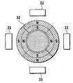
도2a 및 도2b는 본 발명의 포인팅 디바이스의 일실시 형태를 나타내는 도면으로, 도2a는 상면도, 도2b는 도2a의 ⅡB-ⅡB선 단면도이다. 도면 중 11은 자기 센서, 12는 링형 자석, 13은 실리콘 수지, 14는 실장 기판, 15는 스위치 커버이다. 자기 센서(11)는 전술한 바와 같이 X축 및 Y축에 따라서 2개씩 대칭으로 실장 기판(14)에 배치되어 있다. 이 자기 센서(11)는 실장 기판(14)의 표면과 평행한 방향의 자속 밀도를 검지한다.2A and 2B are views showing one embodiment of a pointing device of the present invention, wherein FIG. 2A is a top view and FIG. 2B is a cross-sectional view taken along a line IIB-IIB in FIG. 2A. In the figure,
도2a에 도시하는 구성에서는, 자기 센서(11)를 링 자석(12)의 외주부에 배치하고 있지만, 내주부에 배치하는 것도 가능하다. 자기 센서(11)를 링 자석(12)의 내주부에 배치함으로써, 포인팅 디바이스의 한층 소형화가 가능해진다. 링형 자석(12)은 직경 방향으로 NS의 단극 착자가 되어 있다. NS의 어느 쪽이 외주에 착자되어 있는지에 대해서는 특별히 제한되지 않는다. 또한, 실리콘 수지(13)와 실장 기판(14)의 대향면은 접착되어 있지 않다.In the configuration shown in Fig. 2A, the
실리콘 수지(13)는 외력을 가함으로써 용이하게 변형하고, 그 외력을 제거하면 바로 외력을 가하지 않는 초기 상태로 복귀된다. 즉, 스위치 커버(15)를 조작하여 일정 방향으로 이동시킨 경우, 링형 자석(12)도 마찬가지로 이동하게 된다. 그러나, 외력을 제거하면 바로 초기 상태로 복귀된다. 실리콘 수지(13)를 이용함으로써, 이동 기구와 원점 복귀 수단의 소형화가 가능해진다.The
또한, 링형 자석(12)의 이동은 실장 기판(14)의 표면에 대해 대략 평행 이동하는 구성으로 하면, 저등화가 가능해진다.In addition, if the ring-
링형 자석(12)의 실리콘 수지(13) 상에의 고정 방법은 접착제 등을 이용하는 간이한 방법으로 행할 수 있다. 그 경우, 링형 자석(12)의 실리콘 수지(13)와의 접촉면의 전체면에 접착제를 도포하는 것은 아니고, 외주 부근의 부분은 도포하지 않고 접착함으로써 실리콘 수지(13)의 신축성을 유효하게 이용할 수 있어, 링형 자석(12)의 이동 거리를 크게 취할 수 있으므로 적합하다. 또한, 링형 자석(12)의 위치 결정의 문제가 있으므로, 실리콘 수지(13) 상의 링형 자석(12)의 설치 장소에는 오목부를 마련해 두는 것이 바람직하다.The method of fixing the ring-
또한, 실리콘 수지(13)를 성형할 때, 링형 자석(12)을 나중에 접착하지 않아도 되도록 인서트 성형하는 것도 가능하다.It is also possible to insert-mold the
링형 자석(12)과 실리콘 수지(13)를 고무 자석으로 치환함으로써, 또 다른 저등화도 가능해진다. 실리콘 수지(13)의 일부에 자성 재료를 혼입하여 자석을 형성해도 좋다.By substituting the rubber magnet for the ring-shaped
또한, 접촉식 포인팅 디바이스와 비교하여, 자기 검출식 포인팅 디바이스는 접촉에 의한 부품의 마모가 없어지므로 제품 수명이 향상된다.Further, as compared with the contact type pointing device, the self-detecting type pointing device is free from wear of the parts due to contact, thereby improving the service life of the product.
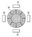
도3a 및 도3b는 본 발명에 있어서의 포인팅 디바이스의 다른 실시 형태를 나타내는 도면으로, 도3a는 상면도, 도3b는 도3a의 ⅢB-ⅢB선 단면도이다. 도2b에 나타낸 실시 형태의 실리콘 수지(13)에 상당하는 실리콘 수지(23)에 오목부를 마련하여, 이 오목부 내에 스위치(28)를 배치하고, 포인팅 디바이스에 스위치 기능을 부여한 것이다. 즉, 실장 기판(24)의 실리콘 수지(23)측에 스위치(28)를 배치한 것이다. 실리콘 수지(23)에는 스위치(28)를 누르기 위한 돌기(26)가 마련되어 있다. 또한, 링형 자석(22)은 네오디의 본드 자석을 이용함으로써 저등화가 가능하게 되어 있다.3A and 3B are views showing another embodiment of the pointing device according to the present invention, wherein FIG. 3A is a top view and FIG. 3B is a sectional view taken along line IIIB-IIIB in FIG. 3A. A recess is provided in the
본래, 포인팅 디바이스는 입력점의 좌표치를 출력하기 위한 디바이스이지만, 스위치 기능을 부여함으로써 좌표치뿐만 아니라 결정 기능을 부여한 포인팅 디바이스가 된다. 스위치 커버(25)를 링형 자석(22)의 방향으로 압입함으로써 스위치 기능을 만족하는 구성으로 되어 있다. 스위치를 설치함으로써, 퍼스널 컴퓨터의 마우스와 마찬가지로 좌표치와 결정의 2 신호를 갖게 된다.Originally, the pointing device is a device for outputting the coordinate value of the input point, but by giving the switch function, it becomes a pointing device that gives the determination function as well as the coordinate value. The
이 스위치(28)로서는, 누름 버튼 스위치 등 어떠한 스위치라도 상관없지만, 누른 것을 확인하기 쉽고(클릭감이 있음), 스위치를 압입한 후에 자동 복귀되는 택틸(tactile) 스위치, 택트(tact) 스위치, 터치(touch) 스위치, 스트로크(stroke) 스위치 등, 대상물과의 물리적 접촉을 이용하여 대상물을 확인하는 스위치가 적합하다.The
또한, 도3b에 나타낸 실시 형태의 실리콘 수지(23)의 링형 자석(22)을 설치한 부분 및 그 근방을 링형 자석(22)을 설치하지 않은 실리콘 수지(23) 부분보다 실리콘 수지(23)의 두께를 얇게 하여 공간부(27)를 마련하고 있다. 링형 자석(22) 하부의 실리콘 수지가 얇을수록 링형 자석(22)의 이동 범위를 크게 취할 수 있으므로, 실리콘 수지(23)의 동작을 전제로 하는 부분에 대해서는 얇게 하는 것이 바람직하다.The portion of the
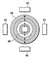
도4a 및 도4b는 본 발명에 있어서의 포인팅 디바이스의 또 다른 실시 형태를 나타내는 도면이다. 도3a에 나타낸 실시 형태에 있어서, 링형 자석의 착자를 내외 단극 착자가 아닌, 각각 내외주를 4극(도4a) 또는 8극(도4b)으로 착자한 것이다. 다극 착자의 링형 자석(32)을 이용함으로써, 자속의 수렴 효과가 강해져 지향성이 상승하므로, 포인팅 디바이스의 출력 감도가 증가하는 것을 기대할 수 있다. 링형 자석(32)의 자극의 수는 자기 센서(31)의 수의 양의 정수배로 함으로써, 자기 센서(31)와 링형 자석(32)의 자극 중심을 대향시키는 것이 가능해져, 높은 신호 출력을 기대할 수 있게 된다. 또한, 신호 처리 부분을 공통화할 수 있다. 즉, 링형 자석(32)이 M극(M = K × I, K : 사용하는 자기 센서의 수, I : 1 이상의 정수)으로 착자되는 것이 바람직하다.4A and 4B are views showing still another embodiment of the pointing device according to the present invention. In the embodiment shown in Fig. 3 (a), the inner and outer circumferences of the ring-like magnet are magnetized into four poles (Fig. 4A) or eight poles (Fig. 4B), respectively. By using the ring-shaped
또한, 링형 자석(32)을 원기둥 형상 자석으로 형상 변경해도 자석 외주부를 마찬가지로 착자하는 것이 가능하다. 다극 착자한 자석을 이용하여 본 발명을 실시할 때에는, 링 형상 이외의 형상을 한 자석을 이용할 수 있다.Even if the ring-
도5는 본 발명에 있어서의 포인팅 디바이스의 또 다른 실시 형태를 나타내는 도면이다. 도2a에 나타낸 실시 형태에 있어서, 링형 자석의 원점 복귀 수단을 강화한 것이다. 전술한 바와 같이, 실리콘 수지 자체에 링형 자석(42)을 원점으로 복귀시키는 능력을 갖고 있지만, 링형 자석(42)의 내부에 또 다른 자석(49)을 설치하여, 서로의 자석의 반발력을 이용하여 원점으로 복귀하도록 되어 있다. 본 실시 형태의 예에서는, 다른 자석(49)은 내외 단극 착자로, 외주에 S극이 배치된다. 이와 같은 구성을 취하면, 실리콘 수지의 시간의 흐름에 따른 열화에 의한 원점 복귀 특성의 악화를 방지할 수 있다.5 is a view showing still another embodiment of the pointing device according to the present invention. In the embodiment shown in Fig. 2A, the origin returning means of the ring-like magnet is reinforced. As described above, the silicone resin itself has the ability to return the ring-shaped
상술한 모든 실시 형태에 대해서는, 자기 센서에 홀 소자를 이용하는 것을 상정하고 있었다. 홀 소자는 출력 단자가 2개 있으므로, 출력 배선의 배치 거리가 길어진다. 따라서, 배선을 위한 공간이 확대되고, 또한 거리가 길기 때문에 외부 노이즈의 영향을 받기 쉬워진다. 그러나, 출력 단자가 1개인 홀 IC나 반도체 자기 저항 효과 소자를 자기 센서로서 이용하는 경우에는 출력 신호선의 수를 저감시킬 수 있으므로, 실장 기판의 공간 절약화와, 외부 노이즈의 영향의 저감을 도모하는 것이 가능해진다.In all of the above-described embodiments, it is assumed that a Hall element is used for the magnetic sensor. Since the Hall element has two output terminals, the arrangement distance of the output wiring becomes long. Therefore, the space for wiring is enlarged and the distance is long, so that it is easily affected by external noise. However, when a Hall IC or semiconductor magnetoresistive effect element having one output terminal is used as a magnetic sensor, the number of output signal lines can be reduced, thereby saving space on the mounting board and reducing the influence of external noise It becomes possible.
또한, 상술한 모든 실시 형태는 실장 기판의 표면에 평행한 자속 밀도를 검지하는 자기 센서를 상정하였지만, 실장 기판 표면과의 이루는 각도(0도 이상 또한 90도 이하)가 약 60도 이하인 자속 밀도를 검지하는 자기 센서이면, 포인팅 디바이스의 S/N은 저하되지만 같은 효과를 얻을 수 있다.Although all of the above embodiments assume a magnetic sensor that detects the magnetic flux density parallel to the surface of the mounting board, the magnetic flux density at an angle (between 0 degrees and 90 degrees) with the surface of the mounting board is about 60 degrees or less If the magnetic sensor detects the S / N of the pointing device, the same effect can be obtained.
또한, 상술한 실시 형태에 대해서는, 링형 자석을 외주 방향으로 착자한 것을 이용하고 있으므로, 스위치 커버 상면으로의 누설 자속 밀도가 극적으로 감소하는 것을 기대할 수 있다. 따라서, 근처에 자기 카드를 근접시킨 경우, 이 자기 카드 등의 정보를 소실하게 되는 문제가 위구되는 것도 없어진다.In the above-described embodiment, since the ring magnet is magnetized in the outer peripheral direction, the leakage magnetic flux density to the upper surface of the switch cover can be expected to be dramatically reduced. Therefore, when the magnetic card is brought close to the vicinity, the problem of losing information such as the magnetic card is eliminated.
본 발명은 상술한 실시 형태에 한정되는 일 없이, 또한 다양하게 변형하여 실시하는 것이 가능하다.The present invention is not limited to the above-described embodiments, and various modifications can be made.
다음에, 본 발명의 구체적인 실시예에 대해 이하에 설명한다.Next, specific embodiments of the present invention will be described below.
(제1 실시예)(Embodiment 1)
상술한 본 발명의 실시 형태의 구성으로 포인팅 디바이스를 구축하였을 때의 출력 특성의 일예에 대해 이하에 설명한다.An example of the output characteristic when the pointing device is constructed with the configuration of the above-described embodiment of the present invention will be described below.
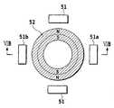
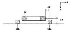
도6a 및 도6b는 본 발명의 포인팅 디바이스의 제1 실시예를 나타내는 도면으로, 도6a가 상면도, 도6b가 도6a의 ⅥB-ⅥB선 단면도이다. 링형 자석(52)은 φ13(외경) × φ8.8(내경)이고, 두께가 0.5(단위는 모두 ㎜)이다. 링형 자석(52)은 내외 단극 착자되어 있고, 외측이 N극, 내측이 S극이다. 링형 자석(52)에는 네오디의 본드 자석을 이용하고, 그 보자력은 460 kA/m이다. 또한, 도면 중 z 방향으로 이동 가능하게 보유 지지되어 있다. 링형 자석(52)의 가동 범위는 z 방향에 ±1.2 ㎜이다. 자기 센서(51)는 홀 소자이고, z 방향의 자속 밀도를 검출하는 타입의 것이다.6A and 6B are views showing a first embodiment of the pointing device of the present invention, in which FIG. 6A is a top view and FIG. 6B is a sectional view taken along a line VIB-VIB in FIG. 6A. The ring-
링형 자석(52)이 원점에 있을 때, 도면 중 z 방향에 있어서의 링형 자석(52)의 외경 단부로부터 자기 센서(51)의 센서 위치까지의 거리를 갭 Z라 하였다. 또한, 도면 중 x 방향에 있어서의 링형 자석(52)의 중심으로부터 자기 센서(51)의 센서 위치까지의 거리를 갭 X라 하였다. 이 때, 링형 자석(52)을 z 방향으로 ±1.2 ㎜ 움직이고, 우측 자기 센서(51a)의 자속 밀도와 좌측 자기 센서(51b)의 자속 밀도의 차를 산출한 결과를 도7에 나타낸다. 단, 이 때의 갭 Z는 2 ㎜로 하고, 갭 X는 0 ㎜, 0.25 ㎜, 0.5 ㎜, 0.75 ㎜의 4가지를 행하였다.When the ring-
갭 X를 0.5 ㎜ 이내로 하면, 링형 자석(52)을 z 방향으로 ±1.2 ㎜ 움직였을 때, ±20 mT 이상의 자속 밀도 변화가 생기고 있는 것을 알 수 있다. 이 자속 밀도 변화의 값은 홀 소자(51)로 검출하는 데 충분한 값이다. 또한, 갭 X를 0에 가 까이 할수록, 자속 밀도의 변화는 커져 포인팅 디바이스로서 유효하게 기능하는 것도 알 수 있다.When the gap X is 0.5 mm or less, it is understood that a magnetic flux density change of ± 20 mT or more occurs when the ring-
마찬가지로, 갭 Z를 1.6 ㎜로 하였을 때의 자속 밀도차를 산출한 결과를 도8에 나타낸다. 갭 Z를 2 ㎜에서 1.6 ㎜로 변경함으로써, 거의 자속 밀도차의 값은 배증하는 것을 알 수 있다. 이상의 결과로부터, 갭 Z와 갭 X의 값을 작게 하면 할수록 포인팅 디바이스의 특성으로서는 양호한 것이 되는 것을 알 수 있다.Similarly, the result of calculating the magnetic flux density difference when the gap Z is 1.6 mm is shown in Fig. By changing the gap Z from 2 mm to 1.6 mm, it can be seen that the value of the magnetic flux density difference almost doubles. From the above results, it can be seen that the smaller the values of the gap Z and the gap X are, the better the characteristic of the pointing device is.
또한, 본 제1 실시예의 포인팅 디바이스의 특히 우수한 점은, 링형 자석(52)이 가동 범위의 한계에 근접하였을 때(본 예에서는 z의 +1.0 ㎜ 이상과 -1.0 ㎜ 이하의 범위), 포인팅 디바이스의 출력이 커지는 점이다. 즉 z가 1.0 ㎜ 이상인 범위와 -1.0 ㎜ 이하인 범위에서는 도7 및 도8에 나타내는 그래프의 기울기가 커져 있다.The pointing device of the first embodiment is particularly advantageous in that when the ring-
예를 들어, 디스플레이 상의 커서를 좌단부로부터 우단부로 이동시킬 때, 조작자는 가능한 한 커서를 빨리 움직이고 싶다고 생각하는 것이 보통이다. 그와 같은 때에, 조작자는 포인팅 디바이스의 링형 자석(52)을 우단부의 가동 범위 한계까지 움직이게 된다. 본 발명의 포인팅 디바이스에서는, 링형 자석(52)의 가동 범위 한계에 근접할수록 커서가 빨리 움직이게 되므로(도7 및 도8에 나타내는 그래프의 기울기가 큰 점을 이용하게 되므로), 보다 사람의 감각에 가까운 특성을 갖고 있다고 할 수 있다.For example, when moving the cursor on the display from the left end to the right end, it is common for the operator to think that he wants to move the cursor as fast as possible. At that time, the operator moves the ring-shaped
또, 종래의 포인팅 디바이스에서는 자석의 가동 범위 한계에 근접하면 커서의 이동 속도가 떨어지게 되는 문제가 있어(후술하는 비교예에서 설명) 조작감을 저하시키고 있었다. 본 발명의 포인팅 디바이스는 상술한 문제를 해소하여 매우 조작감이 향상된다.Further, in the conventional pointing device, the moving speed of the cursor is lowered when approaching the limit of the movable range of the magnet (described in a comparative example to be described later). The pointing device of the present invention solves the above-described problem and greatly improves the operability.
본 제1 실시예에서는, 자기 센서(51)를 링형 자석의 외주부에 배치하였지만, 내주부에 배치해도 같은 효과를 얻을 수 있는 것은 물론이다. 또한, 내주부에 배치함으로써 보다 한층 소형화가 가능해진다.In the first embodiment, the
(제2 실시예)(Second Embodiment)
상술한 본 발명의 실시 형태의 구성으로 포인팅 디바이스를 구축하였을 때의 출력 특성의 다른 일예에 대해 이하에 설명한다.Another example of the output characteristics when the pointing device is constructed with the configuration of the above-described embodiment of the present invention will be described below.
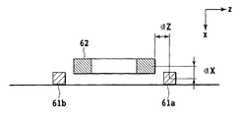
본 제2 실시예의 개략은 상술한 제1 실시예와 마찬가지로 도6a 및 도6b에 도시하는 구성이다. 링형 자석(52)은 φ11.78(외경) × φ5(내경)이고, 두께가 0.485(단위는 모두 ㎜)이다. 링형 자석(52)은 내외 단극 착자되어 있고, 외측이 N극, 내측이 S극이다. 링형 자석(52)에는 네오디의 본드 자석을 이용하고, 그 보자력은 398 kA/m이다. 또한, 도면 중의 z 방향으로 이동 가능하게 보유 지지되어 있다. 링형 자석(52)의 가동 범위는 z 방향에 ±1.2 ㎜이다. 자기 센서(51)는 홀 소자로, z 방향의 자속 밀도를 검출하는 타입의 것이다.The outline of the second embodiment is the configuration shown in Figs. 6A and 6B similarly to the first embodiment described above. The ring-
제1 실시예와 마찬가지로, 링형 자석(52)이 원점에 있을 때, 도면 중 z 방향에 있어서의 링형 자석(52)의 외경 단부로부터 자기 센서(51)의 센서 위치까지의 거리를 갭 Z라 하였다. 또한, 도면 중 x 방향에 있어서의 링형 자석(52)의 중심으로부터 자기 센서(51)의 센서 위치까지의 거리를 갭 X라 하였다. 이 때, 링형 자석(52)을 z 방향으로 ±1.2 ㎜ 움직이고, 우측 자기 센서(51a)의 자속 밀도와 좌측 자기 센서(51b)의 자속 밀도의 차를 산출한 결과를 도9에 나타낸다. 단, 이 때의 갭 X는 0.7805 ㎜로 하고, 갭 Z는 3 ㎜, 2.5 ㎜, 2 ㎜의 3가지를 행하였다.As in the first embodiment, when the ring-shaped
갭 Z를 2 ㎜로 해도, 링형 자석(52)을 z 방향으로 ±1.2 ㎜ 움직였을 때, ±10 mT 정도의 자속 밀도 변화밖에 발생하지 않은 것을 알 수 있다. 이 자속 밀도 변화의 값은 홀 소자(51)로 검출하기에는 약간 어딘가 부족한 값이다.Even when the gap Z is 2 mm, it can be seen that only a change in magnetic flux density of about 10 mT occurs when the ring-
상술한 구성의 포인팅 디바이스를 개선하기 위해, 자기 센서(51)를 z 방향과x 방향의 한가운데, 즉 z축 방향 및 x축 방향에 45도를 이루는 방향의 자속 밀도를 검출하는 타입의 것으로 변경하였다. 단, 그 방향은 링형 자석(52)으로부터의 자속 밀도가 큰 방향으로, 본 제2 실시예에서는 자기 센서(51a)는 우측 하부 방향의 자속 밀도를 검출하는 것이고, 자기 센서(51b)는 좌측 하부 방향의 자속 밀도를 검출하는 것이다. 상술한 구성에서 링형 자석(52)을 z 방향으로 ±1.2 ㎜ 움직여, 우측 자기 센서(51a)의 자속 밀도와 좌측 자기 센서(51b)의 자속 밀도의 차를 산출한 결과를 도10에 나타낸다.In order to improve the pointing device having the above-described configuration, the
z 방향의 자속 밀도를 검지하는 자기 센서로부터 z 방향에 45도의 각도를 이루는 방향의 자속 밀도를 검지하는 자기 센서로 변경함으로써, 대략 자속 밀도차의 값은 2배로 증가하는 것을 알 수 있다. 이상의 결과로부터, 자기 센서의 검지 방향은 z 방향에 한정되는 것은 아니며, 링형 자석(52)과 자기 센서(51)의 배치 관계에 의해 적절하게 변경하는 것이 바람직하다. 단, 자기 센서의 자속 밀도의 검지 방향의 목표로서는, z 방향으로부터 대략 60도 이하로 하면 양호한 결과를 얻을 수 있는 것을 알고 있다.it can be seen that the value of the difference of the magnetic flux density is substantially doubled by changing from the magnetic sensor for detecting the magnetic flux density in the z direction to the magnetic sensor for detecting the magnetic flux density in the direction forming the angle of 45 degrees in the z direction. From the above results, it is preferable that the detection direction of the magnetic sensor is not limited to the z direction but is appropriately changed depending on the arrangement relationship of the ring-
또한, 본 제2 실시예의 포인팅 디바이스의 우수한 점은, 링형 자석(52)이 가동 범위의 한계에 근접하였을 때(본 예에서는 z의 +1.0 ㎜ 이상과 -1.0 ㎜ 이하의 범위), 포인팅 디바이스의 출력이 커지는 점이다. 즉, z가 1.0 ㎜ 이상의 범위와 -1.0 ㎜ 이하의 범위에서는 도10에 나타내는 그래프의 기울기가 커져 있다.The pointing device of the second embodiment is advantageous in that when the ring-
본 제2 실시예에서는 자기 센서(51)를 링형 자석(52)의 외주부에 배치하였지만, 내주부에 배치해도 같은 효과를 얻을 수 있는 것은 물론이다. 또한, 내주부에 배치함으로써 보다 한층 소형화가 가능해진다.Although the
(제3 실시예)(Third Embodiment)
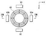
도11a 및 도11b는 본 발명의 포인팅 디바이스의 제3 실시예를 나타내는 도면으로, 도11a가 상면도, 도11b가 도11a의 ⅩⅠB-ⅩⅠB선 단면도이다. 제1 실시예에서 이용한 내외 단극 착자의 링형 자석(52)을 다극 착자의 링형 자석(62)으로 변경한 실시예를 나타내고 있다. 링형 자석(62)은 φ12(외경) × φ8(내경)이고, 두께가 1(단위는 모두 ㎜)이다. 링형 자석(62)은 도11a에 도시한 바와 같이 다극 착자되어 있다. 링형 자석(62)에는 네오디의 본드 자석을 이용하였다. 또한, 도면 중 z 방향과 y 방향으로 이동 가능하게 보유 지지되어 있다. 링형 자석(62)의 가동 범위는 z 방향과 y 방향으로 각각 ±1 ㎜이다. 자기 센서(61)는 홀 소자로, 도11a의 좌우에 배치된 것은 z 방향의 자속 밀도를 검출하는 타입의 것이고, 상하로 배치된 것은 y 방향의 자속 밀도를 검출하는 타입의 것이다.11A and 11B are views showing a pointing device according to a third embodiment of the present invention, wherein FIG. 11A is a top view and FIG. 11B is a sectional view taken along line XIB-XIB in FIG. 11A. An embodiment in which the ring-shaped
링형 자석(62)이 원점에 있을 때, 도면 중 z 방향에 있어서의 링형 자석(62)의 외경 단부로부터 자기 센서(61)의 센서 위치까지의 거리(갭 Z)를 1.6 ㎜로 하였 다. 또한, 도면 중 x 방향에 있어서의 링형 자석(62)의 중심으로부터 자기 센서(61)의 센서 위치까지의 거리(갭 X)를 0 ㎜로 하였다. 이 때, 링형 자석(62)을 z 방향과 y 방향으로 ±1 ㎜ 움직이고, 우측 자기 센서(61a)의 자속 밀도와 좌측 자기 센서(61b)의 자속 밀도의 차를 측정한 결과를 도12에 나타낸다.When the ring-shaped
제1 실시예와 마찬가지로, 포인팅 디바이스의 양호한 출력 특성이 확인할 수 있다. 또한, 포인팅 디바이스의 특성은 y 방향의 위치에 거의 의존하지 않는 것도 알 수 있다. 링형 자석(62)의 가동 범위 한계에 가까운 곳에서는 그래프의 기울기가 커지고, 포인팅 디바이스의 조작감도 향상되고 있는 것을 알 수 있다.As in the first embodiment, good output characteristics of the pointing device can be confirmed. It is also seen that the characteristic of the pointing device is hardly dependent on the position in the y direction. It can be seen that the slope of the graph is large near the limit of the movable range of the ring-
본 제3 실시예에서는 링형 자석(62)을 이용하였지만, 자석의 외주부에 같은 착자를 한 원기둥 형상의 자석을 이용해도 유사한 효과를 확인할 수 있는 것은 물론이다. 또한, 본 제3 실시예에서는 링형 자석(62)의 착자를 내외주 모두 4착자로 하고 있지만, 이 착자 방법에 한정된 것은 아니고, 4극 이외의 다극 착자에서도 같은 효과를 얻을 수 있는 것도 물론이다.Although the ring-shaped
(비교예)(Comparative Example)
종래의 자기 검출식 포인팅 디바이스의 구성의 출력 특성을 이하에 나타낸다.The output characteristics of the configuration of the conventional magnetic detection type pointing device are shown below.
도13은 종래의 포인팅 디바이스의 구성을 도시하는 개략도이다. 자석(72)은 3.9 ㎜ 직사각형이고, 두께가 0.8 ㎜이다. 자석(72)은 도13에 도시한 바와 같이 z 방향으로 착자되어 있다. 자석(72)에는 네오디의 소결 자석을 이용하였다. 또한, 도면 중 x 방향과 y 방향으로 이동 가능하게 보유 지지되어 있다. 자석(72)의 가 동 범위는 양 방향 모두 ±1 ㎜이다. 자기 센서(71)는 아사히까세이 덴시제의 홀 소자 HQ8002(상품명)로, 하나의 패키지 내에 4개의 홀 소자를 갖는 것이다. 또한, 그 홀 소자는 z 방향의 자속 밀도를 검출하는 타입의 것이다. 또한, 대각에 위치하는 홀 소자의 간격은 3.2 ㎜이다. 이 때, 자석(72)을 x 방향과 y 방향으로 ±1 ㎜ 움직이고, HQ8002 내의 우측 자기 센서부의 자속 밀도와 좌측 자기 센서부의 자속 밀도의 차를 측정한 결과를 도14에 나타낸다.13 is a schematic diagram showing the configuration of a conventional pointing device. The
자석(72)이 가동 범위의 한계에 근접하였을 때(본 예에서는 x가 +1.0 ㎜와 -1.0 ㎜에 근접하였을 때), 포인팅 디바이스의 출력이 작아지는 것을 알 수 있다. 즉 x가 1.0 ㎜와 -1.0 ㎜에 근접하면, 도14에 나타내는 그래프의 기울기가 작아지고 있다.It can be seen that the output of the pointing device becomes smaller when the
예를 들어, 디스플레이 상의 커서를 좌단부로부터 우단부로 이동시킬 때, 조작자는 가능한 한 커서를 빨리 움직이고 싶다고 생각하는 것이 보통이다. 그와 같을 때에, 조작자는 포인팅 디바이스의 자석(72)을 우단부의 가동 범위 한계까지 움직이는 것이 된다. 본 비교예의 포인팅 디바이스에서는 자석(72)의 가동 범위 한계에 근접할수록 커서가 천천히 움직이게 되므로(도14에 나타내는 그래프의 기울기가 작은 점을 이용하게 되므로), 사람의 감각과는 다른 특성을 갖고 있다고 할 수 있다. 이 점에서는 사람이 기대하는 조작감을 저하시키고 있어, 개선의 필요가 있는 것은 부정할 수 없다.For example, when moving the cursor on the display from the left end to the right end, it is common for the operator to think that he wants to move the cursor as fast as possible. At that time, the operator moves the
또한, y 방향 위치에 의해 출력 특성이 다르고, 이 점에서도 사람이 기대하는 조작감을 저하시키고 있다고 할 수 있다.In addition, the output characteristic differs depending on the y-direction position, and in this respect, it can be said that the operation feeling expected by a person is lowered.
자기 검출식 포인팅 디바이스에 있어서, 조작감이 양호하며 소형화와 저등화가 가능하고, 또한 외부로의 누설 자속 밀도를 작게 할 수 있고, 또는 제품 수명을 길게 할 수 있으므로, 다양한 어플리케이션에 대해 적합하게 대응하는 것이 가능한 포인팅 디바이스를 제공할 수 있다.In the magnetic detection type pointing device, it is possible to reduce the size of the magnetic sensing device and to reduce the leakage magnetic flux density to the outside, or to prolong the life of the product, It is possible to provide a possible pointing device.
도1은 본 발명의 포인팅 디바이스에 관한 종래예 및 본 발명에 있어서의 포인팅 디바이스의 일예를 나타내는 회로 블록도.1 is a circuit block diagram showing an example of a conventional pointing device of the present invention and an example of a pointing device in the present invention.
도2a 및 도2b는 본 발명에 있어서의 포인팅 디바이스의 일실시 형태를 나타내는 도면.2A and 2B are diagrams showing an embodiment of a pointing device according to the present invention;
도3a 및 도3b는 본 발명에 있어서의 포인팅 디바이스의 다른 실시 형태를 나타내는 도면.3A and 3B are views showing another embodiment of a pointing device according to the present invention;
도4a 및 도4b는 본 발명에 있어서의 포인팅 디바이스의 또 다른 실시 형태를 나타내는 도면.4A and 4B are views showing still another embodiment of a pointing device according to the present invention;
도5는 본 발명에 있어서의 포인팅 디바이스의 또 다른 실시 형태를 나타내는 도면.5 is a view showing still another embodiment of a pointing device according to the present invention;
도6a 및 도6b는 본 발명에 있어서의 포인팅 디바이스의 제1, 제2 실시예를 나타내는 개략도.6A and 6B are schematic views showing first and second embodiments of a pointing device according to the present invention;
도7은 제1 실시예의 구성을 갖는 포인팅 디바이스의 출력 특성예를 나타내는 도면.7 is a view showing an example of an output characteristic of a pointing device having the configuration of the first embodiment;
도8은 제1 실시예의 구성을 갖는 포인팅 디바이스의 다른 출력 특성예를 나타내는 도면.8 is a diagram showing another example of output characteristics of a pointing device having the configuration of the first embodiment;
도9는 제2 실시예의 구성을 갖는 포인팅 디바이스의 다른 출력 특성예를 나타내는 도면.9 is a diagram showing another example of output characteristics of a pointing device having the configuration of the second embodiment;
도10은 제2 실시예의 구성을 갖는 포인팅 디바이스의 다른 출력 특성예를 나 타내는 도면.10 is a view showing another example of output characteristics of the pointing device having the configuration of the second embodiment;
도11a 및 도11b는 본 발명에 있어서의 포인팅 디바이스의 제3 실시예를 나타내는 개략도.11A and 11B are schematic diagrams showing a third embodiment of a pointing device according to the present invention;
도12는 제3 실시예의 구성을 갖는 포인팅 디바이스의 출력 특성예를 나타내는 도면.12 is a diagram showing an example of an output characteristic of a pointing device having the configuration of the third embodiment;
도13은 종래의 포인팅 디바이스의 구성을 도시하는 개략도.13 is a schematic view showing a configuration of a conventional pointing device;
도14는 도13에 도시하는 종래의 포인팅 디바이스의 출력 특성을 나타내는 도면.14 is a diagram showing output characteristics of a conventional pointing device shown in Fig. 13; Fig.
<도면의 주요부분에 대한 간단한 설명>BRIEF DESCRIPTION OF THE DRAWINGS FIG.
11, 21 : 자기 센서11, 21: magnetic sensor
12, 22 : 링형 자석12, 22: ring-shaped magnet
13, 23 : 실리콘 수지13, 23: Silicone resin
14, 24 : 실장 기판14, 24: mounting substrate
28 : 스위치28: Switch
26 : 돌기26: projection
Claims (10)
Translated fromKoreanApplications Claiming Priority (2)
| Application Number | Priority Date | Filing Date | Title |
|---|---|---|---|
| JP2003011291 | 2003-01-20 | ||
| JPJP-P-2003-00011291 | 2003-01-20 |
Related Parent Applications (1)
| Application Number | Title | Priority Date | Filing Date |
|---|---|---|---|
| KR1020057013281ADivisionKR100774067B1 (en) | 2003-01-20 | 2004-01-16 | Pointing device |
Publications (2)
| Publication Number | Publication Date |
|---|---|
| KR20070094022Atrue KR20070094022A (en) | 2007-09-19 |
| KR100847652B1 KR100847652B1 (en) | 2008-07-21 |
Family
ID=32767275
Family Applications (2)
| Application Number | Title | Priority Date | Filing Date |
|---|---|---|---|
| KR1020077017775AExpired - Fee RelatedKR100847652B1 (en) | 2003-01-20 | 2004-01-16 | Pointing device |
| KR1020057013281AExpired - Fee RelatedKR100774067B1 (en) | 2003-01-20 | 2004-01-16 | Pointing device |
Family Applications After (1)
| Application Number | Title | Priority Date | Filing Date |
|---|---|---|---|
| KR1020057013281AExpired - Fee RelatedKR100774067B1 (en) | 2003-01-20 | 2004-01-16 | Pointing device |
Country Status (6)
| Country | Link |
|---|---|
| US (2) | US8054291B2 (en) |
| EP (1) | EP1586983B1 (en) |
| JP (1) | JP4408862B2 (en) |
| KR (2) | KR100847652B1 (en) |
| CN (1) | CN100462903C (en) |
| WO (1) | WO2004066138A1 (en) |
Cited By (3)
| Publication number | Priority date | Publication date | Assignee | Title |
|---|---|---|---|---|
| KR101038483B1 (en)* | 2009-11-17 | 2011-06-01 | 파코스(주) | Pointing device |
| US8143981B2 (en) | 2008-09-26 | 2012-03-27 | Omron Corporation | Input device and electronic apparatus using same |
| KR20210017709A (en)* | 2019-08-09 | 2021-02-17 | 한국기계연구원 | Tactile sensor |
Families Citing this family (46)
| Publication number | Priority date | Publication date | Assignee | Title |
|---|---|---|---|---|
| US20060137396A1 (en)* | 2003-06-03 | 2006-06-29 | Ka Kui Ma | Magnetic jewellery |
| JP2006031399A (en)* | 2004-07-15 | 2006-02-02 | Fujitsu Component Ltd | Pointing device |
| US20060267933A1 (en)* | 2005-05-25 | 2006-11-30 | Li Chong Tai | Eliminating mechanical spring with magnetic forces |
| JP4694392B2 (en)* | 2005-05-30 | 2011-06-08 | 旭化成エレクトロニクス株式会社 | Key sheet for pointing device and pointing device |
| JP4306669B2 (en)* | 2005-10-11 | 2009-08-05 | オムロン株式会社 | Operation input device and electronic apparatus using the same |
| KR100737765B1 (en)* | 2006-05-09 | 2007-07-10 | 삼성전자주식회사 | Tactile support device and method in a portable terminal |
| KR100789725B1 (en)* | 2006-05-15 | 2008-01-02 | 삼성전기주식회사 | Input device |
| US7737945B2 (en)* | 2006-07-28 | 2010-06-15 | Sony Ericsson Mobile Communications Ab | Pointing device with moveable magnetic disc and method |
| US20080068332A1 (en)* | 2006-09-15 | 2008-03-20 | Bernard Lye Hock Chan | Optical input device and method of optically sensing user inputs |
| JP2008111737A (en)* | 2006-10-31 | 2008-05-15 | Furukawa Electric Co Ltd:The | Rotation sensor |
| JP2008111749A (en)* | 2006-10-31 | 2008-05-15 | Furukawa Electric Co Ltd:The | Rotation sensor |
| US7701202B2 (en)* | 2006-11-02 | 2010-04-20 | Massachusetts Institute Of Technology | Compliant tactile sensor that delivers a force vector |
| KR100857166B1 (en)* | 2006-11-29 | 2008-09-05 | 삼성전기주식회사 | Input device and portable terminal having same |
| KR100862950B1 (en)* | 2007-02-14 | 2008-10-15 | 주식회사 이노칩테크놀로지 | Pointing device and portable terminal having same |
| KR100888237B1 (en)* | 2007-07-27 | 2009-03-12 | 주식회사 이노칩테크놀로지 | Pointing device and electronic device including the same |
| US20090115749A1 (en)* | 2007-11-07 | 2009-05-07 | Han Cheol Kim | Input device |
| KR100909546B1 (en)* | 2008-03-04 | 2009-07-27 | 지송학 | Pointing device |
| KR100931071B1 (en)* | 2008-04-14 | 2009-12-10 | 주식회사 이노칩테크놀로지 | How to activate an electronic device and its icon |
| CN102037429A (en)* | 2008-03-20 | 2011-04-27 | 英诺晶片科技股份有限公司 | Electronic device and a pointer motion control method thereof |
| KR101004653B1 (en)* | 2008-04-28 | 2011-01-04 | 주식회사 이노칩테크놀로지 | Electronic device and program control method thereof |
| US8686717B2 (en)* | 2008-09-08 | 2014-04-01 | GM Global Technology Operations LLC | Position sensor arrangement |
| JP5081129B2 (en)* | 2008-10-31 | 2012-11-21 | オムロンオートモーティブエレクトロニクス株式会社 | Switch device for side stand of motorcycle |
| US9870021B2 (en)* | 2009-04-15 | 2018-01-16 | SeeScan, Inc. | Magnetic manual user interface devices |
| WO2010149218A1 (en)* | 2009-06-26 | 2010-12-29 | Continental Teves Ag & Co. Ohg | Hybrid sensor arrangement |
| HUE038039T2 (en) | 2009-12-01 | 2018-09-28 | Translate Bio Inc | Delivery of mrna for the augmentation of proteins and enzymes in human genetic diseases |
| EP2572259A4 (en)* | 2010-05-18 | 2014-10-15 | Seescan Inc | USER INTERFACE DEVICES, APPARATUS AND METHODS |
| PL2717893T3 (en) | 2011-06-08 | 2019-12-31 | Translate Bio, Inc. | Lipid nanoparticle compositions and methods for mRNA delivery |
| WO2013185067A1 (en) | 2012-06-08 | 2013-12-12 | Shire Human Genetic Therapies, Inc. | Nuclease resistant polynucleotides and uses thereof |
| IL290953B2 (en) | 2013-03-14 | 2024-01-01 | Ethris Gmbh | Cftr mrna compositions and related methods and uses |
| AU2014236396A1 (en) | 2013-03-14 | 2015-08-13 | Shire Human Genetic Therapies, Inc. | Methods for purification of messenger RNA |
| KR20240065191A (en)* | 2013-06-11 | 2024-05-14 | 애플 인크. | Wearable electronic device |
| CN106413811A (en) | 2013-10-22 | 2017-02-15 | 夏尔人类遗传性治疗公司 | Mrna therapy for argininosuccinate synthetase deficiency |
| EA201992208A1 (en) | 2013-10-22 | 2020-07-31 | Транслейт Био, Инк. | TREATMENT OF PHENYLKETONURIA USING mRNA |
| WO2015151543A1 (en) | 2014-03-31 | 2015-10-08 | ソニー・オリンパスメディカルソリューションズ株式会社 | Operating device for medical apparatus |
| SG11201608725YA (en) | 2014-04-25 | 2016-11-29 | Shire Human Genetic Therapies | Methods for purification of messenger rna |
| US9759578B2 (en)* | 2015-03-12 | 2017-09-12 | International Business Machines Corporation | Sensor arrangement for position sensing |
| EP3136069B1 (en)* | 2015-08-24 | 2019-10-09 | Magnes Ltd. | A force sensor |
| JP6663259B2 (en)* | 2016-03-15 | 2020-03-11 | エイブリック株式会社 | Semiconductor device and manufacturing method thereof |
| US9962710B2 (en)* | 2016-07-07 | 2018-05-08 | Bunting Magnetics Co. | Magnetic roll |
| CN110114743B (en) | 2016-12-30 | 2022-11-11 | 微软技术许可有限责任公司 | pointing device |
| WO2018157154A2 (en) | 2017-02-27 | 2018-08-30 | Translate Bio, Inc. | Novel codon-optimized cftr mrna |
| US11173190B2 (en) | 2017-05-16 | 2021-11-16 | Translate Bio, Inc. | Treatment of cystic fibrosis by delivery of codon-optimized mRNA encoding CFTR |
| WO2019182651A1 (en)* | 2018-03-23 | 2019-09-26 | Rochester Gauges, Inc | Liquid level gauge with removable indicator assembly |
| EP3841208A1 (en) | 2018-08-24 | 2021-06-30 | Translate Bio, Inc. | Methods for purification of messenger rna |
| WO2020106946A1 (en) | 2018-11-21 | 2020-05-28 | Translate Bio, Inc. | TREATMENT OF CYSTIC FIBROSIS BY DELIVERY OF NEBULIZED mRNA ENCODING CFTR |
| DE102023130262A1 (en) | 2023-11-02 | 2025-05-08 | Eleftherios Vavlas | Magnet arrangement for aligning a tiltable control element to a neutral standard position in a game controller |
Family Cites Families (40)
| Publication number | Priority date | Publication date | Assignee | Title |
|---|---|---|---|---|
| US4029899A (en)* | 1974-11-20 | 1977-06-14 | National Research Development Corporation | Position indicator |
| JPS5866381A (en) | 1981-10-15 | 1983-04-20 | Nec Home Electronics Ltd | Joy stick |
| US4482784A (en)* | 1982-02-01 | 1984-11-13 | Summagraphics Corporation | Position determination device |
| JPS5923420A (en) | 1982-07-28 | 1984-02-06 | 日本電気ホームエレクトロニクス株式会社 | Joy stick |
| JPS5953936A (en) | 1982-09-21 | 1984-03-28 | Nec Home Electronics Ltd | Joy stick type switch |
| US4462594A (en)* | 1982-09-29 | 1984-07-31 | Coleco, Industries, Inc. | Video game with control of rate of movement of game objects |
| US4459578A (en)* | 1983-01-13 | 1984-07-10 | Atari, Inc. | Finger control joystick utilizing Hall effect |
| JPS63298618A (en)* | 1987-05-29 | 1988-12-06 | Graphtec Corp | Wireless system digitizer |
| JPH02240716A (en)* | 1989-03-15 | 1990-09-25 | Matsushita Electric Ind Co Ltd | trackball |
| EP0400953A3 (en)* | 1989-05-31 | 1992-01-08 | Seiko Epson Corporation | Input device |
| JP2953775B2 (en)* | 1990-11-07 | 1999-09-27 | 富士通株式会社 | Pointing control device |
| JPH07117876B2 (en) | 1990-09-18 | 1995-12-18 | 富士通株式会社 | Pointing control device |
| EP0477098B1 (en)* | 1990-09-18 | 1996-06-26 | Fujitsu Limited | Cursor displacement control device for a computer display |
| EP0523002B1 (en)* | 1991-07-11 | 1996-02-28 | LAUBE, Hans-Jürgen | Compound magnet comprising several individual magnets and a permanent magnetic bearing with a compound magnet comprising several individual magnets |
| ATE183017T1 (en)* | 1992-01-30 | 1999-08-15 | Catalysts & Chem Ind Co | WRITING TABLET WITH STYLING PEN AND METHOD FOR PRODUCING |
| JPH0635599A (en) | 1992-07-14 | 1994-02-10 | Fujitsu Ltd | Pointing device |
| JPH06318134A (en)* | 1994-03-15 | 1994-11-15 | Les-Ben:Kk | Data input device |
| JPH08185257A (en) | 1994-10-31 | 1996-07-16 | Matsushita Electric Ind Co Ltd | Coordinate input device |
| JPH08152961A (en) | 1994-11-30 | 1996-06-11 | Fujitsu Ltd | pointing device |
| JPH08227336A (en)* | 1995-02-20 | 1996-09-03 | Wacom Co Ltd | Pressure sensing mechanism and stylus pen |
| JPH0934644A (en) | 1995-07-21 | 1997-02-07 | Oki Electric Ind Co Ltd | Pointing device |
| JP3428255B2 (en) | 1995-10-30 | 2003-07-22 | シャープ株式会社 | Input device such as computer |
| JPH09265347A (en) | 1996-03-28 | 1997-10-07 | Shin Etsu Polymer Co Ltd | Cover member for pointing device |
| US5793668A (en)* | 1997-06-06 | 1998-08-11 | Timeplex, Inc. | Method and apparatus for using parasitic capacitances of a printed circuit board as a temporary data storage medium working with a remote device |
| US6060881A (en)* | 1997-08-06 | 2000-05-09 | Fisher Controls International, Inc. | Flux shaping pole pieces for a magnetic displacement sensor |
| JP2972695B2 (en) | 1998-02-05 | 1999-11-08 | 静岡日本電気株式会社 | Knob for stick switch |
| US7019672B2 (en)* | 1998-12-24 | 2006-03-28 | Synaptics (Uk) Limited | Position sensor |
| JP2000193538A (en) | 1998-12-25 | 2000-07-14 | Nitta Ind Corp | Capacitance-type inner force sensor |
| JP3380996B2 (en) | 1999-02-02 | 2003-02-24 | ニッタ株式会社 | Capacitive force sensor |
| US6373265B1 (en)* | 1999-02-02 | 2002-04-16 | Nitta Corporation | Electrostatic capacitive touch sensor |
| JP3413464B2 (en) | 1999-07-13 | 2003-06-03 | ニッタ株式会社 | Capacitive force sensor |
| WO2001039169A1 (en)* | 1999-11-25 | 2001-05-31 | Ulrich Hermann | Device for simulating a pressure point in keyboards of piano-type keyboard instruments |
| JP4013454B2 (en)* | 2000-06-23 | 2007-11-28 | 富士ゼロックス株式会社 | Pointing device and information processing apparatus |
| GB2367346B (en) | 2000-09-28 | 2004-07-14 | Nokia Mobile Phones Ltd | Control device |
| JP2002149336A (en)* | 2000-11-09 | 2002-05-24 | Nagano Fujitsu Component Kk | Coordinate input device |
| JP2002174532A (en) | 2000-12-07 | 2002-06-21 | Sensatec Co Ltd | Contactless variable voltage device |
| FI116326B (en)* | 2000-12-27 | 2005-10-31 | Nokia Corp | Compact low profile magnetic input device |
| JP4121730B2 (en) | 2001-01-19 | 2008-07-23 | 富士通コンポーネント株式会社 | Pointing device and portable information device |
| ATE419576T1 (en)* | 2001-04-19 | 2009-01-15 | Asahi Kasei Emd Corp | DISPLAY DEVICE |
| JP4175007B2 (en)* | 2002-03-22 | 2008-11-05 | 松下電器産業株式会社 | Rotation operation type input device |
- 2004
- 2004-01-16KRKR1020077017775Apatent/KR100847652B1/ennot_activeExpired - Fee Related
- 2004-01-16JPJP2005508041Apatent/JP4408862B2/ennot_activeExpired - Fee Related
- 2004-01-16EPEP04702792.5Apatent/EP1586983B1/ennot_activeExpired - Lifetime
- 2004-01-16USUS10/542,643patent/US8054291B2/ennot_activeExpired - Fee Related
- 2004-01-16CNCNB2004800024532Apatent/CN100462903C/ennot_activeExpired - Fee Related
- 2004-01-16KRKR1020057013281Apatent/KR100774067B1/ennot_activeExpired - Fee Related
- 2004-01-16WOPCT/JP2004/000272patent/WO2004066138A1/enactiveApplication Filing
- 2011
- 2011-09-22USUS13/240,149patent/US20120007803A1/ennot_activeAbandoned
Cited By (3)
| Publication number | Priority date | Publication date | Assignee | Title |
|---|---|---|---|---|
| US8143981B2 (en) | 2008-09-26 | 2012-03-27 | Omron Corporation | Input device and electronic apparatus using same |
| KR101038483B1 (en)* | 2009-11-17 | 2011-06-01 | 파코스(주) | Pointing device |
| KR20210017709A (en)* | 2019-08-09 | 2021-02-17 | 한국기계연구원 | Tactile sensor |
Also Published As
| Publication number | Publication date |
|---|---|
| EP1586983B1 (en) | 2013-06-05 |
| CN1739089A (en) | 2006-02-22 |
| US20120007803A1 (en) | 2012-01-12 |
| EP1586983A4 (en) | 2007-11-28 |
| KR20050100622A (en) | 2005-10-19 |
| KR100847652B1 (en) | 2008-07-21 |
| JPWO2004066138A1 (en) | 2006-05-18 |
| US8054291B2 (en) | 2011-11-08 |
| EP1586983A1 (en) | 2005-10-19 |
| US20060050053A1 (en) | 2006-03-09 |
| CN100462903C (en) | 2009-02-18 |
| WO2004066138A1 (en) | 2004-08-05 |
| KR100774067B1 (en) | 2007-11-06 |
| JP4408862B2 (en) | 2010-02-03 |
Similar Documents
| Publication | Publication Date | Title |
|---|---|---|
| KR100847652B1 (en) | Pointing device | |
| US6606085B1 (en) | Coordinate input device | |
| KR100582128B1 (en) | Pointing device | |
| US20120112859A1 (en) | Multi-direction input device | |
| US7821500B2 (en) | Inductive joystick | |
| JP5131777B2 (en) | Input device and electronic device using the same | |
| CN102087554A (en) | input device | |
| US10107646B2 (en) | Orientation sensor | |
| JP2006049015A (en) | Input device and electronic equipment using it | |
| JP3400641B2 (en) | Linear displacement detector | |
| JP2003316512A (en) | pointing device | |
| JP5352861B2 (en) | pointing device | |
| JP4475798B2 (en) | pointing device | |
| JPWO2009063799A1 (en) | Input device | |
| KR100573675B1 (en) | Non-contact Joystick-type Pointing Device Using Magnetic Sensor and Its Coordinate Generation Method | |
| WO2008063021A1 (en) | Pointing device and electronic device having the same | |
| KR100833269B1 (en) | Pointing device and portable terminal having same | |
| KR100852163B1 (en) | Pointing device and electronic device having the same | |
| JPH03286326A (en) | coordinate input device | |
| JP2011187024A (en) | Position detection system and multidirectional input device equipped with the same |
Legal Events
| Date | Code | Title | Description |
|---|---|---|---|
| A107 | Divisional application of patent | ||
| A201 | Request for examination | ||
| PA0104 | Divisional application for international application | St.27 status event code:A-0-1-A10-A16-div-PA0104 St.27 status event code:A-0-1-A10-A18-div-PA0104 | |
| PA0201 | Request for examination | St.27 status event code:A-1-2-D10-D11-exm-PA0201 | |
| PG1501 | Laying open of application | St.27 status event code:A-1-1-Q10-Q12-nap-PG1501 | |
| E902 | Notification of reason for refusal | ||
| PE0902 | Notice of grounds for rejection | St.27 status event code:A-1-2-D10-D21-exm-PE0902 | |
| T11-X000 | Administrative time limit extension requested | St.27 status event code:U-3-3-T10-T11-oth-X000 | |
| P11-X000 | Amendment of application requested | St.27 status event code:A-2-2-P10-P11-nap-X000 | |
| P13-X000 | Application amended | St.27 status event code:A-2-2-P10-P13-nap-X000 | |
| E701 | Decision to grant or registration of patent right | ||
| PE0701 | Decision of registration | St.27 status event code:A-1-2-D10-D22-exm-PE0701 | |
| GRNT | Written decision to grant | ||
| PR0701 | Registration of establishment | St.27 status event code:A-2-4-F10-F11-exm-PR0701 | |
| PR1002 | Payment of registration fee | Fee payment year number:1 St.27 status event code:A-2-2-U10-U12-oth-PR1002 | |
| PG1601 | Publication of registration | St.27 status event code:A-4-4-Q10-Q13-nap-PG1601 | |
| R18-X000 | Changes to party contact information recorded | St.27 status event code:A-5-5-R10-R18-oth-X000 | |
| PN2301 | Change of applicant | St.27 status event code:A-5-5-R10-R11-asn-PN2301 St.27 status event code:A-5-5-R10-R13-asn-PN2301 | |
| PR1001 | Payment of annual fee | Fee payment year number:4 St.27 status event code:A-4-4-U10-U11-oth-PR1001 | |
| PR1001 | Payment of annual fee | Fee payment year number:5 St.27 status event code:A-4-4-U10-U11-oth-PR1001 | |
| P22-X000 | Classification modified | St.27 status event code:A-4-4-P10-P22-nap-X000 | |
| FPAY | Annual fee payment | Payment date:20130621 Year of fee payment:6 | |
| PR1001 | Payment of annual fee | Fee payment year number:6 St.27 status event code:A-4-4-U10-U11-oth-PR1001 | |
| FPAY | Annual fee payment | Payment date:20140626 Year of fee payment:7 | |
| PR1001 | Payment of annual fee | Fee payment year number:7 St.27 status event code:A-4-4-U10-U11-oth-PR1001 | |
| FPAY | Annual fee payment | Payment date:20150618 Year of fee payment:8 | |
| PR1001 | Payment of annual fee | Fee payment year number:8 St.27 status event code:A-4-4-U10-U11-oth-PR1001 | |
| FPAY | Annual fee payment | Payment date:20160617 Year of fee payment:9 | |
| PR1001 | Payment of annual fee | Fee payment year number:9 St.27 status event code:A-4-4-U10-U11-oth-PR1001 | |
| FPAY | Annual fee payment | Payment date:20170616 Year of fee payment:10 | |
| PR1001 | Payment of annual fee | Fee payment year number:10 St.27 status event code:A-4-4-U10-U11-oth-PR1001 | |
| LAPS | Lapse due to unpaid annual fee | ||
| PC1903 | Unpaid annual fee | Not in force date:20180716 Payment event data comment text:Termination Category : DEFAULT_OF_REGISTRATION_FEE St.27 status event code:A-4-4-U10-U13-oth-PC1903 | |
| PC1903 | Unpaid annual fee | Ip right cessation event data comment text:Termination Category : DEFAULT_OF_REGISTRATION_FEE Not in force date:20180716 St.27 status event code:N-4-6-H10-H13-oth-PC1903 | |
| R18-X000 | Changes to party contact information recorded | St.27 status event code:A-5-5-R10-R18-oth-X000 |