KR20070091963A - Adaptive linear amplifier - Google Patents
Adaptive linear amplifierDownload PDFInfo
- Publication number
- KR20070091963A KR20070091963AKR1020060021796AKR20060021796AKR20070091963AKR 20070091963 AKR20070091963 AKR 20070091963AKR 1020060021796 AKR1020060021796 AKR 1020060021796AKR 20060021796 AKR20060021796 AKR 20060021796AKR 20070091963 AKR20070091963 AKR 20070091963A
- Authority
- KR
- South Korea
- Prior art keywords
- transistor
- auxiliary
- main
- auxiliary transistor
- bias
- Prior art date
- Legal status (The legal status is an assumption and is not a legal conclusion. Google has not performed a legal analysis and makes no representation as to the accuracy of the status listed.)
- Ceased
Links
- 230000003044adaptive effectEffects0.000titleclaimsabstractdescription17
- 238000000034methodMethods0.000claimsdescription2
- 239000003990capacitorSubstances0.000description15
- 238000004519manufacturing processMethods0.000description3
- 230000003321amplificationEffects0.000description2
- 230000000694effectsEffects0.000description2
- 238000003199nucleic acid amplification methodMethods0.000description2
- 230000007423decreaseEffects0.000description1
- 238000012986modificationMethods0.000description1
- 230000004048modificationEffects0.000description1
Images


Classifications
- H—ELECTRICITY
- H03—ELECTRONIC CIRCUITRY
- H03F—AMPLIFIERS
- H03F1/00—Details of amplifiers with only discharge tubes, only semiconductor devices or only unspecified devices as amplifying elements
- H03F1/32—Modifications of amplifiers to reduce non-linear distortion
- H—ELECTRICITY
- H03—ELECTRONIC CIRCUITRY
- H03F—AMPLIFIERS
- H03F1/00—Details of amplifiers with only discharge tubes, only semiconductor devices or only unspecified devices as amplifying elements
- H03F1/30—Modifications of amplifiers to reduce influence of variations of temperature or supply voltage or other physical parameters
- H03F1/301—Modifications of amplifiers to reduce influence of variations of temperature or supply voltage or other physical parameters in MOSFET amplifiers
- H—ELECTRICITY
- H03—ELECTRONIC CIRCUITRY
- H03F—AMPLIFIERS
- H03F3/00—Amplifiers with only discharge tubes or only semiconductor devices as amplifying elements
- H03F3/189—High-frequency amplifiers, e.g. radio frequency amplifiers
- H03F3/19—High-frequency amplifiers, e.g. radio frequency amplifiers with semiconductor devices only
- H03F3/193—High-frequency amplifiers, e.g. radio frequency amplifiers with semiconductor devices only with field-effect devices
- H—ELECTRICITY
- H03—ELECTRONIC CIRCUITRY
- H03F—AMPLIFIERS
- H03F3/00—Amplifiers with only discharge tubes or only semiconductor devices as amplifying elements
- H03F3/68—Combinations of amplifiers, e.g. multi-channel amplifiers for stereophonics
Landscapes
- Engineering & Computer Science (AREA)
- Power Engineering (AREA)
- Physics & Mathematics (AREA)
- Nonlinear Science (AREA)
- Amplifiers (AREA)
Abstract
Translated fromKoreanDescription
Translated fromKorean도 1은 종래의 증폭기이다.1 is a conventional amplifier.
도 2는 본 발명의 제1 실시예에 따른 적응적 선형 증폭기다.2 is an adaptive linear amplifier according to a first embodiment of the present invention.
도 3은 본 발명의 제1 실시예에 따른 적응적 선형 증폭기의 출력파워 영역을 도시한 그래프이다.3 is a graph showing an output power region of the adaptive linear amplifier according to the first embodiment of the present invention.
** 도면의 주요 부분에 관한 부호의 설명 **** Explanation of symbols on main parts of the drawing **
200: 적응적 선형 증폭기,210: 증폭수단200: adaptive linear amplifier, 210: amplification means
220: 부하단,230: 바이어스 제어수단220: load stage, 230: bias control means
240: 참조 테이블240: reference table
본 발명은 증폭기에 관한 것으로, 더욱 상세하게는 전력 소모가 적으며 선형성이 높은 적응적 선형 증폭기에 관한 것이다.The present invention relates to an amplifier, and more particularly, to an adaptive linear amplifier with low power consumption and high linearity.
도 1은 종래의 증폭기이다.1 is a conventional amplifier.
도시된 바와 같이, 종래의 증폭기(100)는 증폭단(110) 및 부하단(120)을 포함한다.As shown, the
여기서, 증폭단(110)은 트랜지스터(MN1) 및 커패시터(C1)를 포함한다.Here, the
트랜지스터(MN1)의 소오스 단자는 접지된다.The source terminal of transistor MN1 is grounded.
트랜지스터(MN1)의 게이트 단자는 커패시터(C1)의 일단에 접속된다.The gate terminal of the transistor MN1 is connected to one end of the capacitor C1 .
커패시터(C1)의 타단은 입력단(IN)에 접속된다.The other end of the capacitor C1 is connected to the input terminal IN.
트랜지스터(MN1)의 드레인 단자는 부하단(120)의 일단 및 출력단(OUT)에 각각 접속된다.The drain terminal of the transistor MN1 is connected to one end of the
부하단(120)의 타단은 전원전압(VDD)가 인가된다.The other end of the
종래의 증폭기(100)의 동작설명은 다음과 같다.The operation of the
트랜지스터(MN1)의 게이트 단자로 소신호인 입력신호가 인가된다.A small signal is applied to the gate terminal of the transistor MN1 .
트랜지스터(MN1)를 바이어싱 하기 위하여 게이트 단자로 대신호인 바이어스(Bias)가 인가된다.In order to bias the transistor MN1 , a large signal bias is applied to the gate terminal.
이러한 구조에 의하여, 입력단(IN)에 인가된 입력신호를 바이어스(Bias)에 의하여 바이어싱된 트랜지스터(MN1)가 증폭하여 출력단(OUT)으로 출력한다.With this structure, the transistor MN1 biased by the bias Bias amplifies the input signal applied to the input terminal IN and outputs it to the output terminal OUT.
이러한 증폭기(100)를 이용하여 파워 컨트롤(power control)를 할 경우에는 바이어스 포인트를 변경하는 것으로 출력 파워를 조절한다.When power control is performed using the
그러나, 이와 같은 구조의 증폭기(100)를 이용하는 파워 컨트롤은 단순히 출력되는 파워의 크기만 조절되는 단점과 높은 출력파워에 맞추어 바이어스 포인트를 결정하면, 전력소모가 불필요하게 증가되는 단점이 있다.However, the power control using the
상술한 문제점을 해결하기 위한 본 발명의 목적은, 출력 파워영역을 변경할 수 있는 증폭기를 제공하는데 있다.An object of the present invention for solving the above problems is to provide an amplifier capable of changing the output power region.
본 발명의 다른 목적은, 전력소모를 줄이고, 선형성이 높은 증폭기를 제공하는데 있다.Another object of the present invention is to provide an amplifier with high linearity and low power consumption.
상술한 과제를 해결하기 위한 본 발명에 따른 적응적 선형 증폭기는 주 트랜지스터와 보조 트랜지스터부를 포함하고, 상기 주 트랜지스터 및 보조 트랜지스터부는 서로 커플되는 증폭수단 및 상기 주 트랜지스터 및 상기 보조 트랜지스터부에 인가되는 바이어스 전압을 제어하는 바이어스 제어수단을 포함하는 것을 특징으로 한다.An adaptive linear amplifier according to the present invention for solving the above problems includes a main transistor and an auxiliary transistor unit, the main transistor and the auxiliary transistor unit amplification means coupled to each other and a bias applied to the main transistor and the auxiliary transistor unit And bias control means for controlling the voltage.
여기서, 상술한 주 트랜지스터와 보조 트랜지스터부는 서로 병렬로 커플되는것이 바람직하다.Here, it is preferable that the above-described main transistor and the auxiliary transistor portion are coupled in parallel with each other.
여기서, 상술한 보조 트랜지스터부는 제1 보조 트랜지스터 및 제2 보조 트랜지스터를 포함하고, 상기 제1 보조 트랜지스터와 제2 보조 트랜지스터는 서로 병렬 로 커플되는 것이 바람직하다.Here, it is preferable that the above-described auxiliary transistor unit includes a first auxiliary transistor and a second auxiliary transistor, and the first auxiliary transistor and the second auxiliary transistor are coupled to each other in parallel.
여기서, 상술한 바이어스 제어수단은 참조 테이블(Look Up Table)을 참조하여 상기 바이어스 전압을 발생하는 것이 바람직하다.Here, it is preferable that the above-described bias control means generates the bias voltage with reference to a look up table.
여기서, 상술한 참조 테이블은 낮은 출력파워용 바이어스 데이터 및 높은 출력파워용 바이어스 데이터를 포함하는 것이 바람직하다.Here, the above-described reference table preferably includes low output power bias data and high output power bias data.
여기서, 상술한 주 트랜지스터는 포화영역에서 동작하고, 상기 보조 트랜지스터부는 서브문턱(subthreshould) 영역에서 동작하는 것이 바람직하다.Here, it is preferable that the above-described main transistor operates in a saturation region and the auxiliary transistor unit operates in a subthreshould region.
기타 실시예들의 구체적인 사항들은 상세한 설명 및 도면들에 포함되어 있다.Specific details of other embodiments are included in the detailed description and the drawings.
본 발명의 이점 및 특징, 그리고 그것들을 달성하는 방법은 첨부되는 도면과 함께 상세하게 후술 되어 있는 실시예들을 참조하면 명확해질 것이다.Advantages and features of the present invention, and methods for achieving them will be apparent with reference to the embodiments described below in detail in conjunction with the accompanying drawings.
그러나 본 발명은 이하에서 개시되는 실시예들에 한정되는 것이 아니라 서로 다른 다양한 형태로 구현될 수 있으며, 단지 본 실시예들은 본 발명의 개시가 완전하도록 하고, 본 발명이 속하는 기술분야에서 통상의 지식을 가진 자에게 발명의 범주를 완전하게 알려주기 위해 제공되는 것이며, 본 발명은 청구항의 범주에 의해 정의될 뿐이다.However, the present invention is not limited to the embodiments disclosed below, but can be implemented in various different forms, and only the embodiments make the disclosure of the present invention complete, and the general knowledge in the art to which the present invention belongs. It is provided to fully inform the person having the scope of the invention, which is defined only by the scope of the claims.
명세서 전체에 걸쳐 동일 참조 부호는 동일 구성 요소를 지칭한다.Like reference numerals refer to like elements throughout.
이하, 첨부된 도면을 참조하여 본 발명의 바람직한 실시예를 상세히 설명하기로 한다.Hereinafter, exemplary embodiments of the present invention will be described in detail with reference to the accompanying drawings.
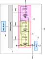
도 2는 본 발명의 제1 실시예에 따른 적응적 선형 증폭기(200)이다.2 is an adaptive
도시된 바와 같이, 본 발명의 제1 실시예에 따른 적응적 선형 증폭기(200)는 증폭수단(210), 부하단(220), 바이어스 제어수단(230) 및 참조 테이블(240)을 포함한다.As shown, the adaptive
여기서, 본 발명의 제1 실시예에 따른 적응적 선형 증폭기(200)의 구성은 다음과 같다.Here, the configuration of the adaptive
증폭수단(210)은 주 트랜지스터(MN21) 및 보조 트랜지스터부(211)를 포함한다.The amplifying
여기서, 주 트랜지스터(MN21)의 신호 입력단에 주 커패시터(C21)를 포함한다.Here, the main capacitor C21 is included in the signal input terminal of the main transistor MN21 .
보조 트랜지스터부(211)는 제1 보조 트랜지스터(MN22a), 제1 보조 커패시터(C22a), 제2 보조 트랜지스터(MN22b) 및 제2 보조 커패시터(C22b)를 포함한다.The
여기서, 본 발명의 제1 실시예에 따른 적응적 선형 증폭기(200)의 연결관계는 다음과 같다.Here, the connection relationship of the adaptive
입력단(IN)은 제1 노드(①)에 연결된다.The input terminal IN is connected to the
주 커패시터(C21)의 일단은 제1 노드(①)에 연결된다.One end of the main capacitor C21 is connected to the
주 커패시터(C21)의 타단은 제2 노드(②)에 연결된다.The other end of the main capacitor C21 is connected to the
주 트랜지스터(MN21)의 신호 입력단(게이트단)은 제2 노드(②)에 연결된다.The signal input terminal (gate terminal) of the main transistor MN21 is connected to the
주 트랜지스터(MN21)의 주전류 경로의 일단(드레인단)은 제6 노드(⑥)에 연 결된다.One end (drain end) of the main current path of the main transistor MN21 is connected to the sixth node (⑥).
주 트랜지스터(MN21)의 주전류 경로의 타단(소오스단)은 제5 노드(⑤)에 연결된다.The other end (source end) of the main current path of the main transistor MN21 is connected to the
제1 보조 커패시터(C22a)의 일단은 제1 노드(①)에 연결된다.One end of the first auxiliary capacitor C22a is connected to the
제1 보조 커패시터(C22a)의 타단은 제3 노드(③)에 연결된다.The other end of the first auxiliary capacitor C22a is connected to the
제1 보조 트랜지스터(MN22a)의 신호 입력단(게이트단)은 제3 노드(③)에 연결된다.The signal input terminal (gate terminal) of the first auxiliary transistor MN22a is connected to the
제1 보조 트랜지스터(MN22a)의 주전류 경로의 일단(드레인단)은 제6 노드(⑥)에 연결된다.One end (drain end) of the main current path of the first auxiliary transistor MN22a is connected to the sixth node (⑥).
제1 보조 트랜지스터(MN22a)의 주전류 경로의 타단(소오스단)은 제5 노드(⑤)에 연결된다.The other end (source end) of the main current path of the first auxiliary transistor MN22a is connected to the
제2 보조 커패시터(C22b)의 일단은 제1 노드(①)에 연결된다.One end of the second auxiliary capacitor C22b is connected to the
제2 보조 커패시터(C22b)의 타단은 제4 노드(④)에 연결된다.The other end of the second auxiliary capacitor C22b is connected to the
제2 보조 트랜지스터(MN22b)의 신호 입력단(게이트단)은 제4 노드(④)에 연결된다.The signal input terminal (gate terminal) of the second auxiliary transistor MN22b is connected to the
제2 보조 트랜지스터(MN22b)의 주전류 경로의 일단(드레인단)은 제6 노드(⑥)에 연결된다.One end (drain end) of the main current path of the second auxiliary transistor MN22b is connected to the sixth node (⑥).
제2 보조 트랜지스터(MN22b)의 주전류 경로의 타단(소오스단)은 제5 노드(⑤)에 연결된다.The other end (source end) of the main current path of the second auxiliary transistor MN22b is connected to the
부하단(220)의 전원단자에는 전원전압(VDD)이 인가된다.The power supply voltage VDD is applied to the power supply terminal of the
부하단(220)의 출력단자에는 제6 노드(⑥)와 출력단(OUT)에 연결된다.The output terminal of the
제5 노드(⑤)는 접지(GND)된다.The
바이어스 제어수단(230)의 주 제어단은 제2 노드(②)에 연결되고, 제1 보조 제어단은 제3 노드(③)에 연결되고, 제2 보조 제어단은 제4 노드(④)에 연결된다.The main control end of the bias control means 230 is connected to the
여기서, 본 발명의 제1 실시예에 따른 적응적 선형 증폭기(200)의 동작설명은 다음과 같다.Here, the operation of the adaptive
주 커패시터(C21), 제1 보조 커패시터(C22a) 및 제2 보조 커패시터(C22b)는 입력단(IN)에 인가된 입력신호의 직류성분을 차단(DC-Blocking)한다.The main capacitor C21 , the first auxiliary capacitor C22a , and the second auxiliary capacitor C22b block DC components of the input signal applied to the input terminal IN.
주 트랜지스터(MN21)는 입력단(IN)에 인가되는 입력신호를 증폭하여 출력단(OUT)으로 출력한다.The main transistor MN21 amplifies an input signal applied to the input terminal IN and outputs it to the output terminal OUT.
주 트랜지스터(MN21)의 채널 폭함수 (Width Function) 와 채널 사이즈와 같은 특성은 제조과정에서 결정되며, 주 트랜지스터(MN21)가 포화영역에서 동작하도록 바이어스 제어수단(230)에 의하여 바이어싱(Bias1) 된다.Properties, such as a channel width function (Width Function) and the channel size of the main transistor (MN21) is, by being determined during the manufacturing process, the main transistor bias control means 230 to operate in the saturation region (MN21) biasing ( Bias1 ).
이러한 구조에 의하여, 주 트랜지스터(MN21)는 일정 크기의gm'' 이 나타나게 되어 회로의 선형성이 낮아지고, 이때의 gm''은 음의 극성을 갖는다.Due to this structure, the main transistor MN21 has a certain magnitude of gm ″, which lowers the linearity of the circuit, and gm ″ has a negative polarity.
여기에서, 주 트랜지스터(MN21)의 gm''이 선형성에 미치는 영향을 작게 하기 위하여 제1 보조 트랜지스터(MN22a) 및 제2 보조 트랜지스터(MN22b)의 양의 극성을 갖는 gm''으로 음의 극성을 갖는 주 트랜지스터(MN21)의 gm''을 상쇄 시킨다.Here, in order to reduce the influence of gm ″ of the main transistor MN21 on the linearity, it is negative that gm ″ has positive polarity of the first auxiliary transistor MN22a and the second auxiliary transistor MN22b . The gm '' of the main transistor MN21 having the polarity is canceled.
즉, 제1 보조 트랜지스터(MN22a) 및 제2 보조 트랜지스터(MN22b)의 채널 폭 함수와 사이즈와 같은 특성은 제조과정에서 결정되며, 제1 보조 트랜지스터(MN22a) 및 제2 보조 트랜지스터(MN22b)가 서브문턱(subthreshould) 영역에서 동작하도록 바이어스 제어수단(230)에 의하여 바이어싱(Bias2a, Bias2b) 된다.That is, characteristics such as the channel width function and the size of the first auxiliary transistor MN22a and the second auxiliary transistor MN22b are determined during the manufacturing process, and the first auxiliary transistor MN22a and the second auxiliary transistor MN are determined during manufacturing.22b ) is biased (Bias2a , Bias2b ) by the bias control means 230 to operate in the subthreshould region.
여기서, 바이어스 제어수단(230)은 참조 테이블(Look Up Table; LUT)를 참조하여 주 트랜지스터(MN21), 제1 보조 트랜지스터(MN22a) 및 제2 보조 트랜지스터(MN22b)의 바이어스 크기를 결정한다.Here, the
결국, 제1 보조 트랜지스터(MN22a) 및 제2 보조 트랜지스터(MN22b)의 음의 영역을 사용하기 위하여 폭함수와 적절한 오프셋 바이어스 값을 조절하는 것이다.As a result, the width function and the appropriate offset bias value are adjusted to use the negative regions of the first auxiliary transistor MN22a and the second auxiliary transistor MN22b .
이러한 구조에 의하여, 입력신호를 주 트랜지스터(MN21)를 이용하여 증폭할 경우에 발생하는 IMD3(3-order Intermodulation Distortion)가 제1 보조 트랜지스터(MN22a) 및 제2 보조 트랜지스터(MN22b)에 의하여 감소한다.With this structure, the 3-order intermodulation distortion (IMD3) generated when the input signal is amplified by using the main transistor MN21 is applied to the first auxiliary transistor MN22a and the second auxiliary transistor MN22b . Decreases.
또한, 바이어스 제어수단(230)은 제1 보조 트랜지스터(MN22a) 및 제2 보조 트 랜지스터(MN22b)의 트랜스 컨덕턴스를 변경함으로써 gm''을 변경한다.In addition, the
따라서, 이러한 변경은 주 트랜지스터(MN21)의 gm''의 값을 제1 보조 트랜지스터(MN22a) 및 제2 보조 트랜지스터(MN22b)의 gm''이 변경하게 되여, 출력 파워 영역을 변경한다.Therefore, such a change causes the value of gm ″ of the main transistor MN21 to be changed by gm ″ of the first auxiliary transistor MN22a and the second auxiliary transistor MN22b , thereby changing the output power region. .
즉, 주 트랜지스터(MN21)와 제1 보조 트랜지스터(MN22a) 및 제2 보조 트랜지스터(MN22b)의 폭함수와 바이어스 포인트를 변경하는 것으로 본 발명의 제1 실시예에 따른 적응적 선형 증폭기(200)의 출력 파워 영역을 달리하게 되면 전력 소모가 줄어들고, 선형성이 높아진다.That is, by changing the width function and the bias point of the main transistor MN21 , the first auxiliary transistor MN22a and the second auxiliary transistor MN22b , the adaptive linear amplifier according to the first embodiment of the present invention ( Changing the output power range of 200) reduces power consumption and increases linearity.
도 3은 본 발명의 제1 실시예에 따른 증폭기의 출력 파워 영역을 도시한 그래프이다.3 is a graph showing an output power region of the amplifier according to the first embodiment of the present invention.
도시된 바와 같이, 본 발명의 제1 실시예에 따른 증폭기의 출력 파워 영역을 도시한 그래프는 3가지 경우의 바이어싱 상태를 포함한다.As shown, the graph showing the output power region of the amplifier according to the first embodiment of the present invention includes the biasing state in three cases.
제1 영역(300)은 주 트랜지스터(MN21)만 바이어스 제어수단(230)에 의하여 바이어싱된 상태의 출력 파워와 IP3에 관한 그래프이다.The
이러한 영역은 종래 기술에서와 같이, 바이어스 포인트를 변경하여 출력 파워를 조절한다.This region modulates the output power by changing the bias point, as in the prior art.
제2 영역(310) 및 제3 영역(320)은 주 트랜지스터(MN21), 제1 보조 트랜지스 터(MN22a) 및 제2 보조 트랜지스터(MN22b)를 바이어스 제어수단(230)에 의하여 바이어싱된 상태의 출력 파워와 IP3에 관한 그래프이다.The
여기서, 제2 영역(310)은 본 발명의 제1 실시예에 따른 적응적 선형 증폭기(200)의 선형성을 높이고 전력 소모를 최소화 하면서 입력 신호를 증폭하여 상대적으로 낮은 출력 파워가 필요한 경우에 유용하다.Here, the
또한, 제3 영역(310)은 본 발명의 제1 실시예에 따른 적응적 선형 증폭기(200)의 선형성을 높이고 전력 소모를 최소화 하면서 입력 신호를 증폭하여 상대적으로 높은 출력 파워가 필요한 경우에 유용하다.In addition, the
이와 같은 구조에 의하여, 출력 파워의 크기에 따라 바이어스 제어수단(230)에 의하여 주 트랜지스터(MN21), 제1 보조 트랜지스터(MN22a) 및 제2 보조 트랜지스터(MN22b)의 바이어싱을 달리 하면, 높은 선형성은 유지되면서 전력소모가 적은 증폭기를 제작할 수 있다.With such a structure, if the biasing of the main transistor MN21 , the first auxiliary transistor MN22a and the second auxiliary transistor MN22b is different by the bias control means 230 according to the magnitude of the output power. Therefore, the amplifier can be manufactured with low power consumption while maintaining high linearity.
이상 첨부된 도면을 참조하여 본 발명의 실시예를 설명하였지만, 상술한 본 발명의 기술적 구성은 본 발명이 속하는 기술 분야의 당업자가 본 발명의 그 기술적 사상이나 필수적 특징을 변경하지 않고서 다른 구체적인 형태로 실시될 수 있다는 것을 이해할 수 있을 것이다.Although the embodiments of the present invention have been described above with reference to the accompanying drawings, the technical configuration of the present invention described above may be modified in other specific forms by those skilled in the art to which the present invention pertains without changing its technical spirit or essential features. It will be appreciated that it may be practiced.
그러므로 이상에서 기술한 실시예들은 모든 면에서 예시적인 것이며 한정적인 것이 아닌 것으로서 이해되어야 하고, 본 발명의 범위는 상기 상세한 설명보다 는 후술하는 특허청구범위에 의하여 나타내어지며, 특허청구범위의 의미 및 범위 그리고 그 등가개념으로부터 도출되는 모든 변경 또는 변형된 형태가 본 발명의 범위에 포함되는 것으로 해석되어야 한다.Therefore, the above-described embodiments are to be understood as illustrative and not restrictive in all respects, and the scope of the present invention is indicated by the appended claims rather than the foregoing description, and the meaning and scope of the claims are as follows. And all changes or modifications derived from the equivalent concept should be interpreted as being included in the scope of the present invention.
상술한 본 발명의 구성에 따르면, 증폭기의 출력 파워영역을 변경하는데 그 효과가 있다.According to the above-described configuration of the present invention, there is an effect in changing the output power region of the amplifier.
또한, 증폭기의 전력소모를 줄이고, 선형성을 높이는데 그 효과가 있다.It also has the effect of reducing power consumption and increasing linearity of the amplifier.
Claims (6)
Translated fromKoreanPriority Applications (5)
| Application Number | Priority Date | Filing Date | Title |
|---|---|---|---|
| KR1020060021796AKR20070091963A (en) | 2006-03-08 | 2006-03-08 | Adaptive linear amplifier |
| EP07103382AEP1833161A1 (en) | 2006-03-08 | 2007-03-02 | Adaptive linear amplifier |
| JP2007053828AJP2007243949A (en) | 2006-03-08 | 2007-03-05 | Adaptive linear amplifier |
| US11/681,893US20070210871A1 (en) | 2006-03-08 | 2007-03-05 | Adaptive linear amplifier |
| CNA2007100864121ACN101034874A (en) | 2006-03-08 | 2007-03-08 | Adaptive linear amplifier |
Applications Claiming Priority (1)
| Application Number | Priority Date | Filing Date | Title |
|---|---|---|---|
| KR1020060021796AKR20070091963A (en) | 2006-03-08 | 2006-03-08 | Adaptive linear amplifier |
Publications (1)
| Publication Number | Publication Date |
|---|---|
| KR20070091963Atrue KR20070091963A (en) | 2007-09-12 |
Family
ID=37905779
Family Applications (1)
| Application Number | Title | Priority Date | Filing Date |
|---|---|---|---|
| KR1020060021796ACeasedKR20070091963A (en) | 2006-03-08 | 2006-03-08 | Adaptive linear amplifier |
Country Status (5)
| Country | Link |
|---|---|
| US (1) | US20070210871A1 (en) |
| EP (1) | EP1833161A1 (en) |
| JP (1) | JP2007243949A (en) |
| KR (1) | KR20070091963A (en) |
| CN (1) | CN101034874A (en) |
Families Citing this family (8)
| Publication number | Priority date | Publication date | Assignee | Title |
|---|---|---|---|---|
| US7508249B2 (en)* | 2005-07-27 | 2009-03-24 | Analog Devices, Inc. | Distributed transistor structure for high linearity active CATV power splitter |
| US8599938B2 (en) | 2007-09-14 | 2013-12-03 | Qualcomm Incorporated | Linear and polar dual mode transmitter circuit |
| US8929840B2 (en) | 2007-09-14 | 2015-01-06 | Qualcomm Incorporated | Local oscillator buffer and mixer having adjustable size |
| US8019310B2 (en) | 2007-10-30 | 2011-09-13 | Qualcomm Incorporated | Local oscillator buffer and mixer having adjustable size |
| WO2009036399A1 (en)* | 2007-09-14 | 2009-03-19 | Qualcomm Incorporated | Local oscillator buffer and mixer having adjustable size |
| US7941115B2 (en) | 2007-09-14 | 2011-05-10 | Qualcomm Incorporated | Mixer with high output power accuracy and low local oscillator leakage |
| US8639205B2 (en) | 2008-03-20 | 2014-01-28 | Qualcomm Incorporated | Reduced power-consumption receivers |
| KR102734914B1 (en) | 2019-06-17 | 2024-11-27 | 삼성전자주식회사 | Dynamic amplifier |
Family Cites Families (6)
| Publication number | Priority date | Publication date | Assignee | Title |
|---|---|---|---|---|
| US3243585A (en)* | 1962-05-29 | 1966-03-29 | North American Aviation Inc | Signal translating apparatus having redundant signal channels |
| US3345578A (en)* | 1964-03-09 | 1967-10-03 | Sylvania Electric Prod | Redundant amplifier circuits |
| JP3033623B2 (en)* | 1990-11-30 | 2000-04-17 | 日本電気株式会社 | Gate bias control circuit and amplifier |
| KR100489693B1 (en) | 2001-02-16 | 2005-05-17 | 인티그런트 테크놀로지즈(주) | Amplifier and Mixer with Improved Linearity |
| US6871049B2 (en)* | 2002-03-21 | 2005-03-22 | Cognio, Inc. | Improving the efficiency of power amplifiers in devices using transmit beamforming |
| US6819184B2 (en)* | 2002-11-06 | 2004-11-16 | Cree Microwave, Inc. | RF transistor amplifier linearity using suppressed third order transconductance |
- 2006
- 2006-03-08KRKR1020060021796Apatent/KR20070091963A/ennot_activeCeased
- 2007
- 2007-03-02EPEP07103382Apatent/EP1833161A1/ennot_activeWithdrawn
- 2007-03-05USUS11/681,893patent/US20070210871A1/ennot_activeAbandoned
- 2007-03-05JPJP2007053828Apatent/JP2007243949A/enactivePending
- 2007-03-08CNCNA2007100864121Apatent/CN101034874A/enactivePending
Also Published As
| Publication number | Publication date |
|---|---|
| EP1833161A1 (en) | 2007-09-12 |
| CN101034874A (en) | 2007-09-12 |
| US20070210871A1 (en) | 2007-09-13 |
| JP2007243949A (en) | 2007-09-20 |
Similar Documents
| Publication | Publication Date | Title |
|---|---|---|
| KR20070091963A (en) | Adaptive linear amplifier | |
| US7884671B2 (en) | Low power operational amplifier | |
| US11316483B2 (en) | Input voltage endurance protection architecture | |
| US8143950B2 (en) | Power amplifier break down characteristic | |
| WO2007109776A3 (en) | Dynamic bias control in power amplifier | |
| CN109274340B (en) | A wideband limiting amplifier circuit | |
| US20120001690A1 (en) | System for Driver Amplifier | |
| JP2015041832A (en) | Power amplifier | |
| JP3731358B2 (en) | High frequency power amplifier circuit | |
| WO2007049390A1 (en) | Differential amplifier | |
| KR100842405B1 (en) | High Voltage CMOS Rail-to-Rail Input / Output Operational Amplifiers | |
| US20060197591A1 (en) | Device and method for enhancing output current driving | |
| Zhao et al. | An approach to essentially improve current efficiency for bulk-driven OTA | |
| CN204442292U (en) | The cascade radio-frequency power amplifier that a kind of efficiency improves | |
| CN101366173A (en) | Power amplifier and its no-load current setting circuit | |
| US7414475B2 (en) | Linearity-improved differential amplification circuit | |
| TWI551040B (en) | Multi class operation power amplifier | |
| Carrillo et al. | 1-V rail-to-rail bulk-driven CMOS OTA with enhanced gain and gain-bandwidth product | |
| KR101320146B1 (en) | Power amplifier module having bias circuit | |
| CN116346047B (en) | Rail-to-rail operational amplifier and input stage structure thereof | |
| CN103684299A (en) | Low-voltage low-power consumption bulk-driven operational amplifier | |
| CN110649893B (en) | Low-power-consumption rail-to-rail driving amplifier circuit | |
| JP3175071B2 (en) | Power amplifier | |
| CN201039088Y (en) | Amplifier structure and amplifier system thereof | |
| KR101653903B1 (en) | Linear amplifier using nonlinear gain stages |
Legal Events
| Date | Code | Title | Description |
|---|---|---|---|
| A201 | Request for examination | ||
| PA0109 | Patent application | Patent event code:PA01091R01D Comment text:Patent Application Patent event date:20060308 | |
| PA0201 | Request for examination | ||
| E902 | Notification of reason for refusal | ||
| PE0902 | Notice of grounds for rejection | Comment text:Notification of reason for refusal Patent event date:20070116 Patent event code:PE09021S01D | |
| AMND | Amendment | ||
| E601 | Decision to refuse application | ||
| PE0601 | Decision on rejection of patent | Patent event date:20070906 Comment text:Decision to Refuse Application Patent event code:PE06012S01D Patent event date:20070116 Comment text:Notification of reason for refusal Patent event code:PE06011S01I | |
| PG1501 | Laying open of application | ||
| J201 | Request for trial against refusal decision | ||
| PJ0201 | Trial against decision of rejection | Patent event date:20071008 Comment text:Request for Trial against Decision on Refusal Patent event code:PJ02012R01D Patent event date:20070906 Comment text:Decision to Refuse Application Patent event code:PJ02011S01I Appeal kind category:Appeal against decision to decline refusal Decision date:20080618 Appeal identifier:2007101010505 Request date:20071008 | |
| AMND | Amendment | ||
| PB0901 | Examination by re-examination before a trial | Comment text:Amendment to Specification, etc. Patent event date:20071010 Patent event code:PB09011R02I Comment text:Request for Trial against Decision on Refusal Patent event date:20071008 Patent event code:PB09011R01I Comment text:Amendment to Specification, etc. Patent event date:20070514 Patent event code:PB09011R02I | |
| B601 | Maintenance of original decision after re-examination before a trial | ||
| E801 | Decision on dismissal of amendment | ||
| PB0601 | Maintenance of original decision after re-examination before a trial | Comment text:Report of Result of Re-examination before a Trial Patent event code:PB06011S01D Patent event date:20071203 | |
| PE0801 | Dismissal of amendment | Patent event code:PE08012E01D Comment text:Decision on Dismissal of Amendment Patent event date:20071203 Patent event code:PE08011R01I Comment text:Amendment to Specification, etc. Patent event date:20071010 Patent event code:PE08011R01I Comment text:Amendment to Specification, etc. Patent event date:20070514 | |
| J301 | Trial decision | Free format text:TRIAL DECISION FOR APPEAL AGAINST DECISION TO DECLINE REFUSAL REQUESTED 20071008 Effective date:20080618 | |
| PJ1301 | Trial decision | Patent event code:PJ13011S01D Patent event date:20080618 Comment text:Trial Decision on Objection to Decision on Refusal Appeal kind category:Appeal against decision to decline refusal Request date:20071008 Decision date:20080618 Appeal identifier:2007101010505 |