KR20070088614A - Method for manufacturing a semiconductor device comprising a metal gate electrode - Google Patents
Method for manufacturing a semiconductor device comprising a metal gate electrodeDownload PDFInfo
- Publication number
- KR20070088614A KR20070088614AKR1020077008086AKR20077008086AKR20070088614AKR 20070088614 AKR20070088614 AKR 20070088614AKR 1020077008086 AKR1020077008086 AKR 1020077008086AKR 20077008086 AKR20077008086 AKR 20077008086AKR 20070088614 AKR20070088614 AKR 20070088614A
- Authority
- KR
- South Korea
- Prior art keywords
- layer
- semiconductor device
- manufacturing
- dielectric layer
- sacrificial
- Prior art date
- Legal status (The legal status is an assumption and is not a legal conclusion. Google has not performed a legal analysis and makes no representation as to the accuracy of the status listed.)
- Granted
Links
Images


Classifications
- H—ELECTRICITY
- H10—SEMICONDUCTOR DEVICES; ELECTRIC SOLID-STATE DEVICES NOT OTHERWISE PROVIDED FOR
- H10D—INORGANIC ELECTRIC SEMICONDUCTOR DEVICES
- H10D84/00—Integrated devices formed in or on semiconductor substrates that comprise only semiconducting layers, e.g. on Si wafers or on GaAs-on-Si wafers
- H10D84/01—Manufacture or treatment
- H10D84/0123—Integrating together multiple components covered by H10D12/00 or H10D30/00, e.g. integrating multiple IGBTs
- H10D84/0126—Integrating together multiple components covered by H10D12/00 or H10D30/00, e.g. integrating multiple IGBTs the components including insulated gates, e.g. IGFETs
- H10D84/0165—Integrating together multiple components covered by H10D12/00 or H10D30/00, e.g. integrating multiple IGBTs the components including insulated gates, e.g. IGFETs the components including complementary IGFETs, e.g. CMOS devices
- H—ELECTRICITY
- H01—ELECTRIC ELEMENTS
- H01L—SEMICONDUCTOR DEVICES NOT COVERED BY CLASS H10
- H01L21/00—Processes or apparatus adapted for the manufacture or treatment of semiconductor or solid state devices or of parts thereof
- H01L21/02—Manufacture or treatment of semiconductor devices or of parts thereof
- H01L21/04—Manufacture or treatment of semiconductor devices or of parts thereof the devices having potential barriers, e.g. a PN junction, depletion layer or carrier concentration layer
- H01L21/18—Manufacture or treatment of semiconductor devices or of parts thereof the devices having potential barriers, e.g. a PN junction, depletion layer or carrier concentration layer the devices having semiconductor bodies comprising elements of Group IV of the Periodic Table or AIIIBV compounds with or without impurities, e.g. doping materials
- H01L21/28—Manufacture of electrodes on semiconductor bodies using processes or apparatus not provided for in groups H01L21/20 - H01L21/268
- H01L21/28008—Making conductor-insulator-semiconductor electrodes
- H01L21/28017—Making conductor-insulator-semiconductor electrodes the insulator being formed after the semiconductor body, the semiconductor being silicon
- H01L21/28026—Making conductor-insulator-semiconductor electrodes the insulator being formed after the semiconductor body, the semiconductor being silicon characterised by the conductor
- H01L21/28114—Making conductor-insulator-semiconductor electrodes the insulator being formed after the semiconductor body, the semiconductor being silicon characterised by the conductor characterised by the sectional shape, e.g. T, inverted-T
- H—ELECTRICITY
- H10—SEMICONDUCTOR DEVICES; ELECTRIC SOLID-STATE DEVICES NOT OTHERWISE PROVIDED FOR
- H10D—INORGANIC ELECTRIC SEMICONDUCTOR DEVICES
- H10D64/00—Electrodes of devices having potential barriers
- H10D64/01—Manufacture or treatment
- H10D64/017—Manufacture or treatment using dummy gates in processes wherein at least parts of the final gates are self-aligned to the dummy gates, i.e. replacement gate processes
- H—ELECTRICITY
- H10—SEMICONDUCTOR DEVICES; ELECTRIC SOLID-STATE DEVICES NOT OTHERWISE PROVIDED FOR
- H10D—INORGANIC ELECTRIC SEMICONDUCTOR DEVICES
- H10D64/00—Electrodes of devices having potential barriers
- H10D64/20—Electrodes characterised by their shapes, relative sizes or dispositions
- H10D64/27—Electrodes not carrying the current to be rectified, amplified, oscillated or switched, e.g. gates
- H10D64/311—Gate electrodes for field-effect devices
- H10D64/411—Gate electrodes for field-effect devices for FETs
- H10D64/511—Gate electrodes for field-effect devices for FETs for IGFETs
- H10D64/517—Gate electrodes for field-effect devices for FETs for IGFETs characterised by the conducting layers
- H10D64/518—Gate electrodes for field-effect devices for FETs for IGFETs characterised by the conducting layers characterised by their lengths or sectional shapes
- H—ELECTRICITY
- H10—SEMICONDUCTOR DEVICES; ELECTRIC SOLID-STATE DEVICES NOT OTHERWISE PROVIDED FOR
- H10D—INORGANIC ELECTRIC SEMICONDUCTOR DEVICES
- H10D84/00—Integrated devices formed in or on semiconductor substrates that comprise only semiconducting layers, e.g. on Si wafers or on GaAs-on-Si wafers
- H10D84/01—Manufacture or treatment
- H10D84/0123—Integrating together multiple components covered by H10D12/00 or H10D30/00, e.g. integrating multiple IGBTs
- H10D84/0126—Integrating together multiple components covered by H10D12/00 or H10D30/00, e.g. integrating multiple IGBTs the components including insulated gates, e.g. IGFETs
- H10D84/0165—Integrating together multiple components covered by H10D12/00 or H10D30/00, e.g. integrating multiple IGBTs the components including insulated gates, e.g. IGFETs the components including complementary IGFETs, e.g. CMOS devices
- H10D84/0172—Manufacturing their gate conductors
- H10D84/0179—Manufacturing their gate conductors the gate conductors having different shapes or dimensions
- H—ELECTRICITY
- H10—SEMICONDUCTOR DEVICES; ELECTRIC SOLID-STATE DEVICES NOT OTHERWISE PROVIDED FOR
- H10D—INORGANIC ELECTRIC SEMICONDUCTOR DEVICES
- H10D84/00—Integrated devices formed in or on semiconductor substrates that comprise only semiconducting layers, e.g. on Si wafers or on GaAs-on-Si wafers
- H10D84/01—Manufacture or treatment
- H10D84/02—Manufacture or treatment characterised by using material-based technologies
- H10D84/03—Manufacture or treatment characterised by using material-based technologies using Group IV technology, e.g. silicon technology or silicon-carbide [SiC] technology
- H10D84/038—Manufacture or treatment characterised by using material-based technologies using Group IV technology, e.g. silicon technology or silicon-carbide [SiC] technology using silicon technology, e.g. SiGe
- H—ELECTRICITY
- H01—ELECTRIC ELEMENTS
- H01L—SEMICONDUCTOR DEVICES NOT COVERED BY CLASS H10
- H01L21/00—Processes or apparatus adapted for the manufacture or treatment of semiconductor or solid state devices or of parts thereof
- H01L21/02—Manufacture or treatment of semiconductor devices or of parts thereof
- H01L21/04—Manufacture or treatment of semiconductor devices or of parts thereof the devices having potential barriers, e.g. a PN junction, depletion layer or carrier concentration layer
- H01L21/18—Manufacture or treatment of semiconductor devices or of parts thereof the devices having potential barriers, e.g. a PN junction, depletion layer or carrier concentration layer the devices having semiconductor bodies comprising elements of Group IV of the Periodic Table or AIIIBV compounds with or without impurities, e.g. doping materials
- H01L21/30—Treatment of semiconductor bodies using processes or apparatus not provided for in groups H01L21/20 - H01L21/26
- H01L21/302—Treatment of semiconductor bodies using processes or apparatus not provided for in groups H01L21/20 - H01L21/26 to change their surface-physical characteristics or shape, e.g. etching, polishing, cutting
- H01L21/306—Chemical or electrical treatment, e.g. electrolytic etching
- H01L21/30604—Chemical etching
- H01L21/30608—Anisotropic liquid etching
- Y—GENERAL TAGGING OF NEW TECHNOLOGICAL DEVELOPMENTS; GENERAL TAGGING OF CROSS-SECTIONAL TECHNOLOGIES SPANNING OVER SEVERAL SECTIONS OF THE IPC; TECHNICAL SUBJECTS COVERED BY FORMER USPC CROSS-REFERENCE ART COLLECTIONS [XRACs] AND DIGESTS
- Y10—TECHNICAL SUBJECTS COVERED BY FORMER USPC
- Y10S—TECHNICAL SUBJECTS COVERED BY FORMER USPC CROSS-REFERENCE ART COLLECTIONS [XRACs] AND DIGESTS
- Y10S438/00—Semiconductor device manufacturing: process
- Y10S438/926—Dummy metallization
Landscapes
- Engineering & Computer Science (AREA)
- Physics & Mathematics (AREA)
- Condensed Matter Physics & Semiconductors (AREA)
- General Physics & Mathematics (AREA)
- Manufacturing & Machinery (AREA)
- Computer Hardware Design (AREA)
- Microelectronics & Electronic Packaging (AREA)
- Power Engineering (AREA)
- Insulated Gate Type Field-Effect Transistor (AREA)
- Electrodes Of Semiconductors (AREA)
Abstract
Description
Translated fromKorean본 발명은 반도체 디바이스의 제조 방법에 관한 것으로, 보다 구체적으로는, 금속 게이트 전극을 구비한 반도체 디바이스의 제조 방법에 관한 것이다.TECHNICAL FIELD This invention relates to the manufacturing method of a semiconductor device. More specifically, It is related with the manufacturing method of the semiconductor device provided with the metal gate electrode.
금속 게이트 전극을 포함하는 CMOS 디바이스 제조 시, 서로 다른 금속으로 게이트 전극을 형성하는 데에 대체 게이트 프로세스(replacement gate process)가 사용될 수 있다. 이 프로세스에서, 한 쌍의 스페이서에 의해 브래킷된(bracketed) 제 1 폴리실리콘 층이 제거되어 스페이서 사이에 트렌치를 형성할 수 있다. 이 트렌치는 제 1 금속으로 충진된다. 그 다음 제 2 폴리실리콘 층이 제거되어, 제 1 금속과는 다른 제 2 금속으로 대체된다.In fabricating CMOS devices that include metal gate electrodes, a replacement gate process can be used to form gate electrodes from different metals. In this process, the first polysilicon layer bracketed by a pair of spacers can be removed to form trenches between the spacers. This trench is filled with a first metal. The second polysilicon layer is then removed and replaced with a second metal other than the first metal.
이러한 대체 게이트 프로세스에서, (금속으로 대체될) 제 1 및 제 2 폴리실리콘 층은 이어서 형성되는 금속 게이트 전극에서의 게이트 길이를 정의하는 에칭된 폴리실리콘 층이다. 특정한 애플리케이션에서, 45nm인 (또는 이보다 짧은) 게이트 길이를 갖는 금속 게이트 전극을 생산해야할 수 있다. 그러나, 종래의 포토리소 그래픽 기술을 사용하여 고 볼륨 제조(high volume manufacturing)에 적합한 약 45nm(또는 그 미만)의 폭을 갖는 에칭된 폴리실리콘 층을 형성하는 것은 불가능할 수 있다.In this alternate gate process, the first and second polysilicon layers (to be replaced by metal) are subsequently etched polysilicon layers that define the gate length at the metal gate electrode formed. In certain applications, it may be necessary to produce a metal gate electrode with a gate length of 45 nm (or shorter). However, it may be impossible to form an etched polysilicon layer having a width of about 45 nm (or less) suitable for high volume manufacturing using conventional photolithographic graphics techniques.
극도로 얇은 에칭된 폴리실리콘 층을 형성하는 것이 어려울 뿐 아니라, 만약 패터닝된 폴리실리콘 층이 실질적으로 수직인 측벽을 구비하는 경우, 이것은 또 다른 문제를 발생시킬 수 있다. 이러한 패터닝된 폴리실리콘 층을 제거한 후, 다양한 재료를 사용하여 결과적인 트렌치의 측벽을 균일하게 코팅하는 것이 어려울 수 있다. 또한, 트렌치 중심에 공간이 생성되어 이러한 트렌치를 금속을 사용하여 완전히 충진하는 것이 불가능할 수 있다.Not only is it difficult to form an extremely thin etched polysilicon layer, but if the patterned polysilicon layer has substantially vertical sidewalls, this can create another problem. After removing this patterned polysilicon layer, it may be difficult to uniformly coat the sidewalls of the resulting trench using various materials. In addition, space may be created in the center of the trench, making it impossible to completely fill the trench with metal.
따라서, 금속 게이트 전극을 포함하는 반도체 디바이스의 개선된 형성 방법에 대한 필요성이 존재한다. 또한 금속 게이트 전극 형성을 촉진시키는 프로파일을 갖는 동시에, 45nm(또는 그 미만)의 게이트 길이를 가능케 하는 패터닝된 희생 구조체의 생성 방법에 대한 필요성이 존재한다. 본 발명은 그러한 방법을 제공한다.Accordingly, there is a need for an improved method of forming a semiconductor device comprising a metal gate electrode. There is also a need for a method of producing a patterned sacrificial structure that has a profile that facilitates metal gate electrode formation, while at the same time allowing a gate length of 45 nm (or less). The present invention provides such a method.
도 1a 내지 도 1l는 본 발명의 방법의 실시예를 실행할 때 형성될 수 있는 구조체의 단면도.1A-1L are cross-sectional views of structures that may be formed when practicing embodiments of the method of the present invention.
첨부된 도면에 도시된 형태는 실제 축적대로 도시되지 않았다.The form shown in the accompanying drawings is not drawn to scale.
본 명세서에는 반도체 디바이스의 제조 방법이 개시되었다. 이 방법은 기판 상에 유전층을 형성하고, 유전층 상에 제 1 층 및 제 2 층을 포함하는 희생 구조체를 형성하는 단계를 포함하며, 이때 제 2 층은 제 1층보다 넓다. 트렌치를 생성하도록 희생 구조체를 제거한 후, 트렌치 내에 금속 게이트 전극이 형성된다.Disclosed herein is a method of manufacturing a semiconductor device. The method includes forming a dielectric layer on a substrate and forming a sacrificial structure comprising a first layer and a second layer on the dielectric layer, wherein the second layer is wider than the first layer. After removing the sacrificial structure to create a trench, a metal gate electrode is formed in the trench.
하기의 설명에서, 본 발명에 대한 철저한 이해를 제공하도록 다수의 세부 사항이 설정되었다. 그러나, 당업자에게, 본 발명이 본 명세서에 특별히 기술된 것과는 다른 다양한 방법으로 실시될 수 있다는 점은 명백할 것이다. 따라서 본 발명이 하기에 기술된 특정 세부 사항으로 제한되는 것은 아니다.In the following description, numerous details are set forth in order to provide a thorough understanding of the present invention. However, it will be apparent to one skilled in the art that the present invention may be practiced in various ways other than as specifically described herein. Thus, the present invention is not limited to the specific details described below.
도 1a 내지 도 1l는 본 발명의 방법의 실시예를 실행할 때 형성될 수 있는 구조체의 단면도이다. 먼저, 제 1 유전층(101)이 기판(100) 상에 형성되고, 제 1 유전층(101) 상에 제 1 층(102)이 형성되고, 제 1 층(102) 상에 제 2 층(103)이 형성되어 도 1a의 구조체가 생성된다. 기판(100)은 반도체 디바이스가 자신의 위에 설계될 수 있는 기반으로서의 역할을 할 수 있는 임의의 재료를 포함할 수 있다. 제 1 유전층(101)은 실리콘 이산화물, 질화규소 이산화물, 높은-k 유전층, 또는 기판(100)을 보호할 수 있는 다른 재료를 포함할 수 있다.1A-1L are cross-sectional views of structures that may be formed when practicing embodiments of the method of the present invention. First, a first
이 실시예에서, 제 1 층(102)d은 적절한 습식 에칭 프로세스를 사용하여 제거될 수 있는 재료를 포함할 수 있다. 제 1 층(102)은, 예를 들어, 실리콘, 실리콘을 포함하는 합금, 게르마늄, 또는 게르마늄을 포함하는 합금을 포함할 수 있다. 제 1 층(102)은 바람직하게 약 100Å 내지 약 500Å의 두께를 가질 수 있다. 제 2 층(103)은, 제 1 층(102)과 같이, 실리콘, 실리콘을 포함하는 합금, 게르마늄, 또 는 게르마늄을 포함하는 합금을 포함할 수 있다. 제 2 층(103)은 바람직하게 약 400Å 내지 약 800Å의 두께를 가질 수 있다. 당업자에게 명백한 바와 같이, 제 1 유전층(101), 제 1 층(102) 및 제 3 층(103)은 종래의 프로세스 단계를 사용하여 형성될 수 있다.In this embodiment, the first layer 102d may include a material that can be removed using a suitable wet etching process. The
이러한 실시예에서, 제 1 층(102)은 선택적으로 제거될 수 있는 재료를 포함해야 한다. 예를 들어, 만약 제 1 층(102)이 게르마늄을 포함한다면, 제 2 층(103)은 적절한 에칭 화학 작용을 받았을 때 제 1 층(102)이 제거되는 것보다 느린 속도로 제거될 수 있는 실리콘 또는 다른 재료를 포함해야 한다. 이와 유사하게, 제 1 층(102)이 실리콘을 포함하면, 제 2 층(103)은 제 1 층(102)이 제거되는 속도보다 느린 속도로 제거될 수 있는 게르마늄 또는 다른 재료를 포함해야 한다. 제 1 층(102) 및 제 2 층(103)이 형성될 수 있는 재료의 몇몇 예가 본 명세서에 명시되었지만, 제 2 층(103)에 대해 선택적으로 제 1 층(102)이 제거되도록 하는 다양한 다른 재료가 본 발명의 사상 및 범주로부터 벗어나지 않는 범위에서 대신 사용될 수 있다.In this embodiment, the
도 1a의 구조체를 형성한 후, 도 1b의 구조체를 생성하기 위해 종래의 리소그래피 및 건식 에칭 프로세스를 사용하여 제 1 층(102) 및 제 2 층(103)이 패터닝될 수 있다. 바람직한 실시예에서, 프로세스 내의 이 단계에서의 제 1 층(102) 및 제 2 층(103)은 각각 약 1000Å 미만의 폭을 가져야 하며, 바람직하게는 약 400Å 내지 약 600Å의 폭을 가져야 한다.After forming the structure of FIG. 1A, the
도 1b의 구조체가 형성된 후, 제 2 층(103)보다 제 1 층(102)을 실질적으로 더 제거하는 수용액에 제 1 층(102) 및 제 2 층(103)을 노출시킴으로써 희생 구조체(104, 114)가 형성된다. 그 결과, 제 2 층(103)은 제 1 층(102)보다 더 넓다. 만약 제 1 층(102)이 게르마늄을 포함하고 제 2 층(103)이 실리콘을 포함한다면, 희생 구조체(104, 114)는 층(102, 103)을 과산화수소를 포함하는 수용액에 노출시킴으로써 형성될 수 있다. 바람직한 실시예에서, 이러한 수용액은 부피 단위로 약 2% 내지 약 5%의 과산화수소를 포함한다. 이러한 솔루션은 부피 단위로 약 1% 내지 약 10%의 수산화암모늄을 더 포함할 수 있다.After the structure of FIG. 1B is formed, the
만약 제 1 층(102)이 실리콘을 포함하고 제 2 층(103)이 게르마늄을 포함한다면, 희생 구조체(104, 114)는 층(102, 103)을 예를 들어, 수산화암모늄 또는 테트라메틸 수산화암모늄("TMAH": tetramethyl ammonium hydroxide)과 같은 수산화물 소스를 포함하는 수용액에 노출시킴으로써 형성될 수 있다. 바람직한 실시예에서, 이러한 수용액은 부피의 단위로 약 2% 내지 약 15%의 수산화암모늄 또는 TMAH를 포함한다. 제 1 층(102) 부분은 제 1 층(102)이 제 2 층(103)의 폭보다 적어도 약 100Å 더 작은 폭을 가질 때까지 제거될 수 있다. 특히 바람직한 실시예에서, 제 1 층(102)은, 이 층의 일부분이 제거된 후 약 300Å 미만의 폭을 갖는다. 희생 구조체(104, 114)가 형성된 후, 도 1c의 구조체를 형성하도록 제 1 유전층(101)의 커버되지 않은 부분이 예를 들어 종래의 에칭 프로세스를 통해 제거될 수 있다.If the
하기에서 설명된 바와 같이, 하단의 제 1 희생층보다 넓은 제 2 희생층을 포함하는 희생 구조체를 형성하는 데에 본 발명의 방법을 적용하는 것은 금속 게이트 전극을 포함하는 매우 작은 트랜지스터를 형성하는 데에 대체 게이트 프로세스를 사용하는 것을 가능케 한다. 도 1d 내지 도 1l는 본 발명의 방법을 이러한 프로세스에 결합하였을 때 형성될 수 있는 구조체를 도시한다.As described below, applying the method of the present invention to form a sacrificial structure comprising a second sacrificial layer that is wider than the first sacrificial layer at the bottom is used to form a very small transistor comprising a metal gate electrode. It is possible to use an alternative gate process for 1D-1L illustrate structures that can be formed when incorporating the method of the present invention into such a process.
도 1c의 구조체를 형성한 후, 제 2 유전층(105)이 디바이스 위에 증착되어 도 1d의 구조체를 형성할 수 있다. 제 2 유전층(105)은 예를 들어 실리콘 이산화물 또는 낮은-k 재료를 포함할 수 있다. 프로세스의 이러한 단계에 의해, 소스 및 드레인 영역이 미리 형성된다. 당업자에게 명확한 바와 같이, 종래의 프로세스 단계, 재료 및 장비가 이러한 구조체를 생성하는 데에 사용될 수 있다. 이와 관련하여, 처음 증착되었을 때, 희생 구조체(104, 114) 상에 형성된 제 2 유전층(105)의 부분을 제거하는 데에 종래의 화학적 기계적 폴리싱("CMP") 동작이 사용될 수 있다.After forming the structure of FIG. 1C, a second
도 1d의 구조체를 형성한 후, 제 2 유전층(105) 내에 둘러싸인 트렌치(106)를 생성하도록 희생 구조체(104)가 제거되어 도 1e의 구조체를 생성한다. 바람직한 실시예에서, 희생 구조체(104)를 제거하는 데에 습식 에칭 프로세스가 사용된다. 이러한 습식 에칭 프로세스는 희생 구조체(104)를 적절한 수용액, 또는 솔루션에 충분한 온도에서 충분한 시간 동안 노출시켜 실질적으로 전체 희생 구조체(104)를 제거하는 것을 포함할 수 있다.After forming the structure of FIG. 1D, the
예를 들어, 만약 제 1 층(102)이 게르마늄을 포함하고 제 2 층(103)이 실리콘을 포함하면, 희생 구조체(104)를 제거하는 데에 두 단계의 습식 에칭 프로세스가 사용될 수 있다. 상단의 실리콘 층을 제거하도록, 이 층은 부피의 단위로 2% 내지 15%의 수산화암모늄 또는 TMAH를 포함하는 수용액에 노출될 수 있다. 상단의 층 을 제거한 후, 하단의 게르마늄 층을 제거하도록, 이 층은 부피의 단위로 약 2% 내지 약 5%의 과산화수소 및 부피의 단위로 약 1% 내지 약 10%의 수산화암모늄을 포함하는 수용액에 노출될 수 있다.For example, if the
만약, 대신 제 1 층(102)이 실리콘을 포함하고 제 2 층(103)이 게르마늄을 포함하면, 희생 구조체(104)는 이러한 동일한 두 가지의 습식 에칭 단계를 역순으로 사용하여 제거될 수 있다. 상단의 게르마늄 층을 제거하도록, 이 층은 부피의 단위로 약 2% 내지 약 5%의 과산화수소 및 부피의 단위로 약 1% 내지 약 10%의 수산화암모늄을 포함하는 수용액에 노출될 수 있다. 상단의 층을 제거한 후, 하단의 실리콘 층을 제거하도록, 이 층은 부피의 단위로 2% 내지 15%의 수산화암모늄 또는 TMAH를 포함하는 수용액에 노출될 수 있다. 희생 구조체(104)가 제거될 때, 하단의 기판(100)을 보호하도록 제 1 유전층(101)을 유지해야할 수 있다.If instead the
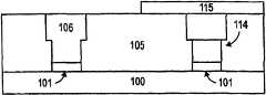
도 1e에 도시된 바와 같이, 희생 구조체(104)가 제거될 때, 희생 구조체(104)를 제거하기에 앞서 희생 구조체(114)의 제거를 방지하기 위해 희생 구조체(114) 상에 마스크(115)가 형성된다. 마스크(115)는 종래의 프로세스 및 마스킹 재료를 이용하여 형성될 수 있다. 희생 구조체(104)가 제거된 후, 마스크(115)가 제거될 수 있다.As shown in FIG. 1E, when
트렌치(106)를 형성하도록 희생 구조체(104)가 제거되었을 때, 희생 구조체(104)의 제 2 층(103)이 하단의 제 1 층(102)보다 넓었기 때문에 결과적인 트렌치는 바닥보다 상부가 더 넓은 폭을 갖는다. 이러한 트렌치의 측면은 바닥과 상부가 같은 폭을 갖는 트렌치의 측면보다 더 균일하게 코팅될 수 있다. 또한, 이러한 트렌치를 금속으로 충진하는 것은, 트렌치 중심에 공간이 형성되지 않으며 바닥과 상부가 같은 폭을 갖는 트렌치를 충진하는 경우에 비교하여 더 용이할 수 있다.When the
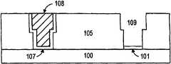
이러한 실시예에서, 희생 구조체(104)를 제거한 후, 하단 부분인 제 1 유전층(101)이 제거된다. 제 1 유전층(101)이 실리콘 이산화물을 포함할 때, 도 1f의 구조체를 형성하도록, 이것은 실리콘 이산화물에 대해 선택적인 에칭 프로세스를 사용하여 제거될 수 있다. 이러한 에칭 프로세스는 탈이온수 내에 약 1%의 HF를 포함하는 솔루션에 층(101)을 노출시키는 것을 포함할 수 있다. 제 1 유전층(101)을 제거하기 위한 에칭 프로세스는 제 2 유전층(105)의 일부도 제거할 수 있기 때문에, 층(101)은 예를 들어 약 60초 미만의 제한된 시간 동안 노출되어야 한다.In this embodiment, after removing the
제 1 유전층(101)을 제거한 후, 이 실시예에서 높은-k인 게이트 유전층(107)이 기판(100) 상의 트렌치(106) 내에 형성되어 도 1g의 구조체를 형성한다. 높은-k 게이트 유전층(107)을 제조하는 데에 사용될 수 있는 일부 재료는, 하프늄 산화물, 하프늄 실리콘 산화물, 란탄 산화물, 란탄 알루미늄 산화물, 지르코늄 산화물, 지르코늄 실리콘 산화물, 탄탈 산화물, 티타늄 산화물, 바륨 스트론튬 티타늄 산화물, 바륨 티타늄 산화물, 스트론튬 티타늄 산화물, 이트륨 산화물, 알루미늄 산화물, 납 스칸듐 탄탈 산화물 및 납 아연 니오브산염을 포함한다. 특히 바람직한 재료는 하프늄 산화물, 지르코늄 산화물 및 알루미늄 산화물이다. 높은-k인 게이트 유전층(107)을 형성하는 데에 사용될 수 있는 재료의 몇몇 예가 본 명세서에서 개시되었지만, 이 층은 다른 재료로 제조될 수도 있다. After removing the
높은-k 게이트 유전층(107)은 예를 들어, 종래의 화학적 증착("CVD"), 저압 CVD, 또는 물리적 증착("PVD") 프로세스와 같은 종래의 증착 방법을 사용하여 기판(100) 상에 형성될 수 있다. 바람직하게는, 종래의 원자층 CVD 프로세스가 사용된다. 이 프로세스에서, 금속 산화물 전구체(precursor)(예를 들어, 금속 클로라이드) 및 스팀(steam)이 선택된 유속으로 CVD 리액터에 제공될 수 있으며, 선택된 온도 및 압력에서 동작되어 기판(100)과 높은-k 게이트 유전층(107) 사이에 원자적으로 원만한 경계면을 생성한다. CVD 리액터는 원하는 두께를 갖는 층을 형성하기 위해 충분히 긴 시간 동안 동작되어야 한다. 대부분의 애플리케이션에서, 높은-k 게이트 유전층(107)은 약 60Å 미만의 두께를 가져야 하고, 보다 바람직하게는 약 5Å 내지 약 40Å의 두께를 갖는다.The high-k
도 1g에 도시된 바와 같이, 높은-k 게이트 유전층(107)을 형성하는 데에 원자층 CVD 프로세스가 사용되었을 때, 이 층은 트렌치의 바닥 위에 형성될 뿐만 아니라 트렌치(106)의 측면 상에도 형성될 것이다. (도 1g는 처음 증착되었을 때 제 2 유전층(105) 상에 형성된 높은-k 게이트 유전층(107)의 부분이 제거된 구조체를 도시한다.) 만약 높은-k 게이트 유전층(107)이 산화물을 포함하면, 이것을 제조하는 데에 사용된 프로세스에 의존하여, 임의의 표면 부분에서의 산소 공동 및 바람직하지 않은 불순물 레벨을 나타낼 수 있다. 층(107)이 형성된 후, 거의 이상화된 금속:산소 화학량론을 갖는 층을 생성하도록 층(107)으로부터 불순물을 제거하고 산화시켜야할 수 있다.As shown in FIG. 1G, when an atomic layer CVD process is used to form the high-k
이 층으로부터 불순물을 제거하고 이 층의 산소 함유량을 증가시키기 위해, 높은-k 게이트 유전층(107)에 습식 화학적 처리가 사용될 수 있다. 이러한 습식 화 학적 처리는, 높은-k 게이트 유전층(107)으로부터 불순물을 제거하고 높은-k 게이트 유전층(107)의 산소 함유량을 증가시키도록, 높은-k 게이트 유전층(107)을 충분한 온도에서 충분한 시간 동안 과산화수소를 포함하는 솔루션에 노출시키는 것을 포함할 수 있다. 높은-k 게이트 유전층(107)이 노출되는 적절한 시간 및 온도는 높은-k 게이트 유전층(107)에 대해 원하는 두께 및 다른 특성에 의존할 수 있다.To remove impurities from this layer and increase the oxygen content of this layer, wet chemical treatment may be used for the high-k
높은-k 게이트 유전층(107)이 과산화수소 기반의 솔루션에 노출될 때, 부피의 단위로 약 2% 내지 약 30%의 과산화수소를 포함하는 수용액이 사용될 수 있다. 이러한 노출 단계는 적어도 약 1분간 약 15℃ 내지 약 40℃의 온도에서 수행되어야 한다. 특히 바람직한 실시예에서, 높은-k 게이트 유전층(107)은 약 25℃의 온도에서 약 10분간 부피의 단위로 약 6.7%의 H2O2를 함유하는 수용액에 노출된다. 이러한 노출 단계 동안, 약 10㎑ 내지 약 2,000㎑의 주파수이며, 약 1 내지 약 10watts/㎠에서 소산되는 음파 에너지를 사용하는 것을 필요로 할 수 있다. 바람직한 실시예에서, 약 5watts/㎠에서 소산되는, 약 1,000㎑ 주파수에서의 음파 에너지가 사용될 수 있다.When the high-k
일부 실시예에서, 이러한 프로세스 단계가 희생 구조체(114)를 현저하게 에칭하지 않는 것을 보장하도록 이러한 습식 화학적 처리 동안 (예를 들어 마스크(115)를 유지함으로써) 희생 구조체(114)를 마스킹해야 할 수 있다. 만약 높은-k 게이트 유전층(107)에 이러한 습식 화학적 처리가 적용되는 동안 희생 구조체(114)가 마스킹되면, 마스크는 이러한 프로세스 단계 후에 제거될 수 있다.In some embodiments, it may be necessary to mask the
도 1g에 도시되지 않았지만, 높은-k 게이트 유전층(107) 상에 5 단분자막 두께 이하의 캡핑층이 형성되어야 할 수 있다. 이러한 캡핑층은 높은-k 게이트 유전층(107) 상에 1 내지 5 단분자막의 실리콘 또는 다른 재료를 스퍼터링함으로써 형성될 수 있다. 캡핑층은 예를 들어 플라스마 인핸스된 화학적 증착(PECVD-plasma enhanced chemical vapor deposition) 프로세스 또는 산화제를 포함하는 솔루션을 사용함으로써 산화되어 캡핑 유전체 산화물을 형성할 수 있다.Although not shown in FIG. 1G, a capping layer less than 5 monolayer thick may be formed on the high-k
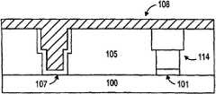
일부 실시예에서 게이트 유전층(107) 상에 캡핑층을 형성해야할 수 있지만, 도시된 실시예에서, 트렌치(106)를 충진하여 도 1h의 구조체를 생성하기 위해 n-형 금속층(108)이 층(107) 상에 직접 형성될 수 있다. n-형 금속층(108)은 금속 NMOS 게이트 전극이 파생될 수 있는 n-형 도전성 재료를 포함할 수 있다. n-형 금속 층(108)을 형성하는 데에 사용될 수 있는 재료는, 하프늄, 지르코늄, 티타늄, 탄탈, 알루미늄 및 예를 들어 이러한 원소를 포함하는 금속 탄화물, 즉 하프늄 탄화물, 지르코늄 탄화물, 티타늄 탄화물, 탄탈 탄화물 및 알루미늄 탄화물과 같은 그들의 합금을 포함할 수 있다. n-형 금속층(108)은 이와는 달리 예를 들어 하프늄, 지르코늄, 티타늄, 탄탈 또는 텅스텐을 포함하는 알루미나이드를 포함할 수 있다.In some embodiments it may be necessary to form a capping layer on the
n-형 금속층(108)은 예를 들어 종래의 스퍼터링 또는 원자층 CVD 프로세스와 같은 잘 알려진 PVD 또는 CVD 프로세스를 사용하여 높은-k 게이트 유전층(107) 상에 형성될 수 있다. 도 1i에 도시된 바와 같이, n-형 금속층(108)은 트렌치(106)를 충진한 부분을 제외하고 제거된다. 층(108)은 적절한 CMP 동작을 통해 디바이스의 다른 부분으로부터 제거될 수 있다. 제 2 유전층(105)은 층(108)이 자신의 표면으 로부터 제거될 때, 폴리싱 스톱으로서의 역할을 할 수 있다.The n-
n-형 금속층(108)은 약 3.9V 내지 약 4.2V의 일함수를 갖는 금속 NMOS 게이트 전극으로서의 역할을 하는 것이 바람직하다. 도 1h 내지 도 1i에 도시된 구조체에서는 n-형 금속층(108)이 트렌치(106)의 전체를 충진하지만, 다른 실시예에서, n-형 금속층(108)은 예를 들어 텅스텐, 알루미늄, 티타늄 또는 질화티타늄과 같이 쉽게 폴리싱될 수 있는 재료를 사용하여 충진되는 트렌치 부분을 남겨둔 채, 트렌치(106)의 단지 부분만을 충진할 수 있다.The n-
도시된 실시예에서, 트렌치(106) 내에 n-형 금속층(108)을 형성한 후, 희생 구조체(114)가 제거되어 제 2 유전층(105) 내에 둘러싸인 트렌치(109)를 생성함으로써 도 1j의 구조체를 생성한다. 바람직한 실시예에서, 희생 구조체(104)를 제거하는 데에 사용된 습식 에칭 프로세스와 동일한 프로세스가 희생 구조체(114)를 제거하는 데에 사용될 수 있다. 일부 실시예에서, 희생 구조체(114) 및 n-형 금속층(108)을 제조하는 재료와, 희생 구조체(114)를 제거하는 프로세스는 희생 구조체(114)가 n-형 금속층(108)으로부터 선택적으로 제거될 수 있도록 한다. 그러나, 만약 희생 구조체(114)가 n-형 금속층(108)으로부터 선택적으로 제거될 수 없으면, 희생 구조체(114)를 제거하기에 앞서 n-형 금속층(108)을 마스킹해야 할 필요성이 있을 수 있다.In the illustrated embodiment, after forming the n-
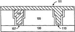
희생 구조체(114)가 제거된 후, 전술된 것과 동일한 프로세스 단계를 사용하여 하단 부분인 제 1 유전층(101)이 제거되고 높은-k 게이트 유전층(110)으로 대체된다. 선택적으로, 전술된 바와 같이, (증착된 후 산화될 수 있는) 트렌치(109)를 p-형 금속으로 충진하기에 앞서 캡핑층이 높은-k 게이트 유전층(110) 상에 형성될 수 있다. 그러나, 이 실시예에서, 제 1 유전층(101)을 높은-k 게이트 유전층(110)으로 대체한 후, p-형 금속층(111)이 트렌치(109)를 충진하도록 높은-k 게이트 유전층(110) 상에 직접 형성되어 도 1k의 구조체를 생성한다.After the
p-형 금속층(111)은 금속 PMOS 게이트 전극이 파생될 수 있는 임의의 p-형 도전성 재료를 포함할 수 있다. p-형 금속층(111)을 형성하는 데에 사용될 수 있는 재료는 루테늄, 팔라듐, 백금, 코발트, 니켈 및 예를 들어 산화루테늄과 같은 도전성 금속 산화물을 포함한다. p-형 금속층(111)은 예를 들어 종래의 스퍼터링 또는 원자층 CVD 프로세스와 같은 잘 알려진 PVD 또는 CVD 프로세스를 사용하여 높은-k 게이트 유전층(110) 상에 형성될 수 있다. 도 1l에 도시된 바와 같이, p-형 금속층(111)은 트렌치(109)를 충진하는 부분을 제외하고 제거된다. 층(111)은 적절한 CMP 동작을 통해 디바이스의 다른 부분으로부터 제거될 수 있으며, 이때 제 2 유전층(105)은 폴리싱 스톱으로서의 역할을 한다. p-형 금속층(111)은 약 4.9eV 내지 약 5.2eV의 일함수를 갖는 금속 PMOS 게이트 전극으로서의 역할을 할 수 있다.The p-
도 1k 내지 도 1l에 도시된 구조체에서는 p-형 금속층(111)이 트렌치(109) 전체를 충진하지만, 다른 실시예에서, p-형 금속층(111)은 트렌치(109)의 단지 부분만을 충진할 수 있다. 금속 NMOS 게이트 전극에서와 같이, 트렌치의 나머지 부분은 예를 들어, 텅스텐, 알루미늄, 티타늄 또는 질화티타늄과 같이 쉽게 폴리싱될 수 있는 재료로 충진될 수 있다. 금속층(108, 111)을 형성하는 재료의 몇몇 예가 본 명세서에 개시되었지만, 이러한 금속층이 다양한 다른 재료로 제조될 수 있다는 점이 당업자에게 명백할 것이다. 이 실시예는 금속 PMOS 게이트 전극을 형성하기에 앞서 금속 NMOS 게이트 전극을 형성하도록 기술되었지만, 다른 실시예에서 금속 NMOS 게이트 전극을 형성하기에 앞서 금속 PMOS 게이트 전극이 형성될 수 있다.In the structure shown in FIGS. 1K-1L, the p-
설명된 실시예에서, 희생 구조체(104, 114)가 제거된 후 제 1 유전층(101)은 높은-k 게이트 유전층으로 대체된다. 다른 실시예에서, 제 1 유전층(101)은 희생 구조체(104, 114)가 제거된 후에도 유지되는 높은-k 게이트 유전층을 포함할 수 있다. 이러한 다른 실시예에서, 금속층(108, 111)은 제 1 유전층(101)을 높은-k 게이트 유전층으로 제 1 대체 하지 않고 제 1 유전층(101) 상에 직접 형성된다.In the described embodiment, the
전술된 실시예에서, 마스크(115)는 희생 구조체(104)가 제거될 때 희생 구조체(114)가 제거되는 것을 방지한다. 다른 실시예에서, 마스크(115)는 희생 구조체(114) 상에 형성되지 않는다. 대신, 두 개의 희생 구조체(104, 114)가, 예를 들어 적절한 습식 에칭 프로세스에 의해 동시에 제거된다. 두 개의 희생 구조체(104, 114)가 동시에 제거된 후, NMOS 및 PMOS 금속 게이트 전극이 다양한 방법으로 형성될 수 있다.In the embodiment described above, the
두 개의 희생 구조체(104, 114)를 동시에 제거한 후 NMOS 및 PMOS 금속 게이트 전극이 형성될 수 있는 한 방법은 제 1 금속층을 오직 트렌치(106) 또는 트렌치(109) 내에만 형성하는 것으로 시작한다. 제 1 금속층은, 두 개의 트렌치 내에 금속층을 증착시키고, 두 개의 트렌치 중 하나의 트렌치 내에 형성된 금속층을 마스킹하고, 노출된 금속을 마스킹되지 않은 다른 트렌치로부터 제거한 후, 마스크를 제거함으로써 오직 하나의 트렌치 내에만 형성될 수 있다. 오직 하나의 트렌치 내 에만 제 1 금속층을 형성한 후, 두 개의 트렌치 내에 제 2 금속층이 증착되어 하나의 트렌치 내의 제 1 금속층을 커버하고, 다른 트렌치 내의 높은-k 게이트 유전층을 커버한다. 이러한 다른 실시예에서, 제 1 금속층은 디바이스(즉, NMOS 또는 PMOS) 중 하나에 대한 일함수를 설정할 수 있으며, 제 2 금속층은 디바이스 중 다른 하나에 대한 일함수를 설정할 수 있다.One way in which NMOS and PMOS metal gate electrodes can be formed after simultaneously removing two
두 개의 희생 구조체(104, 114)를 동시에 제거한 후 NMOS 및 PMOS 금속 게이트 전극을 형성하는 다른 방법도, 두 개의 트렌치 내에 단일 금속층을 증착시키는 것으로 시작한다. 이 금속층의 부분은 마스킹 및 제거되지 않고, 이것의 부분(또는 부분들)은 NMOS 및 PMOS 디바이스에 대해 원하는 일함수를 설정하도록 수정된다. 기술된 실시예가 본 발명의 방법이 대체 게이트 프로세스에서 사용될 수 있는 방법의 예를 제공하지만, 당업자는 이러한 방법이 다양한 다른 방법으로 프로세스에 결합되어 사용될 수 있다는 점을 인지할 것이다.Another method of forming the NMOS and PMOS metal gate electrodes after simultaneously removing the two
트렌치(109)를 충진하는 부분을 제외하고 금속층(111)을 제거한 후, 종래의 증착 프로세스를 사용하여 (도시되지 않은) 캡핑 유전층이 제 2 유전층(105), 금속 NMOS 게이트 전극(108) 및 금속 PMOS 게이트 전극(111) 상에 증착될 수 있다. 예를 들어, 디바이스의 콘택트, 금속 상호접속부 및 패시베이션 층의 형성과 같이, 이러한 캡핑 유전층의 증착 후 디바이스를 완성하기 위해 이어지는 프로세스 단계는 당업자에게 잘 알려져 있으며 본 명세서에서 기술되지 않을 것이다.After removing the
전술된 방법은 종래의 포토리소그래픽 기술이 수행하는 것보다 더욱 짧은 길이의 게이트를 구비하는 금속 게이트 전극을 갖는 트랜지스터의 형성을 가능케 할 수 있다. 또한, 전술된 방법은 선택된 재료를 사용하여 측면이 균일하게 코팅될 수 있고 자신의 중심에 공간이 생성되지 않은 채 금속으로 완전히 충진될 수 있는 좁은 트렌치가 형성되는 것을 가능케 할 수 있다. 전술된 실시예는 이러한 트렌치를 포함하는 디바이스를 형성하는 프로세스의 예를 제공하지만, 본 발명이 이러한 특정 실시예로 제한되는 것은 아니다.The method described above may enable the formation of transistors with metal gate electrodes having gates of shorter length than conventional photolithographic techniques perform. In addition, the method described above may enable the formation of narrow trenches that may be uniformly coated on the sides using selected materials and may be completely filled with metal without creating a space in its center. The above-described embodiment provides an example of a process for forming a device including such a trench, but the present invention is not limited to this particular embodiment.
전술된 설명이 본 발명에서 사용될 수 있는 특정한 단계 및 재료를 포함하지만, 당업자는 다양한 변경 및 대체가 가능하다는 점을 이해할 것이다. 따라서, 그러한 모든 변경, 대안, 대체 및 첨부는 첨부된 특허청구범위에 의해 정의된 본 발명의 사상 및 범주 내에 포함되는 것으로 간주된다.Although the foregoing description includes specific steps and materials that can be used in the present invention, those skilled in the art will understand that various changes and substitutions are possible. Accordingly, all such modifications, alternatives, substitutions and attachments are considered to be included within the spirit and scope of the invention as defined by the appended claims.
Claims (20)
Translated fromKoreanApplications Claiming Priority (2)
| Application Number | Priority Date | Filing Date | Title |
|---|---|---|---|
| US10/936,114US7176090B2 (en) | 2004-09-07 | 2004-09-07 | Method for making a semiconductor device that includes a metal gate electrode |
| US10/936,114 | 2004-09-07 |
Publications (2)
| Publication Number | Publication Date |
|---|---|
| KR20070088614Atrue KR20070088614A (en) | 2007-08-29 |
| KR100880038B1 KR100880038B1 (en) | 2009-01-22 |
Family
ID=35583492
Family Applications (1)
| Application Number | Title | Priority Date | Filing Date |
|---|---|---|---|
| KR1020077008086AExpired - Fee RelatedKR100880038B1 (en) | 2004-09-07 | 2005-09-02 | Method for manufacturing a semiconductor device comprising a metal gate electrode |
Country Status (5)
| Country | Link |
|---|---|
| US (1) | US7176090B2 (en) |
| KR (1) | KR100880038B1 (en) |
| CN (1) | CN100565842C (en) |
| TW (1) | TWI292181B (en) |
| WO (1) | WO2006029061A1 (en) |
Families Citing this family (46)
| Publication number | Priority date | Publication date | Assignee | Title |
|---|---|---|---|---|
| DE102007041207B4 (en)* | 2007-08-31 | 2015-05-21 | Globalfoundries Dresden Module One Limited Liability Company & Co. Kg | CMOS device with gate insulation layers of different type and thickness and method of manufacture |
| US7763943B2 (en)* | 2007-12-26 | 2010-07-27 | Intel Corporation | Reducing external resistance of a multi-gate device by incorporation of a partial metallic fin |
| US8030163B2 (en)* | 2007-12-26 | 2011-10-04 | Intel Corporation | Reducing external resistance of a multi-gate device using spacer processing techniques |
| US20090206404A1 (en)* | 2008-02-15 | 2009-08-20 | Ravi Pillarisetty | Reducing external resistance of a multi-gate device by silicidation |
| US8264048B2 (en)* | 2008-02-15 | 2012-09-11 | Intel Corporation | Multi-gate device having a T-shaped gate structure |
| JP4548521B2 (en)* | 2008-07-09 | 2010-09-22 | ソニー株式会社 | Semiconductor device manufacturing method and semiconductor device |
| US8735235B2 (en) | 2008-08-20 | 2014-05-27 | Taiwan Semiconductor Manufacturing Company, Ltd. | Integrated circuit metal gate structure and method of fabrication |
| US8110877B2 (en) | 2008-12-19 | 2012-02-07 | Intel Corporation | Metal-insulator-semiconductor tunneling contacts having an insulative layer disposed between source/drain contacts and source/drain regions |
| US7915127B2 (en)* | 2009-07-27 | 2011-03-29 | United Microelectronics Corp. | Manufacturing method of semiconductor device |
| US8076735B2 (en)* | 2009-10-02 | 2011-12-13 | United Microelectronics Corp. | Semiconductor device with trench of various widths |
| KR101634748B1 (en)* | 2009-12-08 | 2016-07-11 | 삼성전자주식회사 | method for manufacturing MOS transistor and forming method of integrated circuit using the sime |
| CN102468146B (en)* | 2010-11-01 | 2013-12-04 | 中芯国际集成电路制造(上海)有限公司 | Method for forming metal gates |
| CN102468145A (en)* | 2010-11-01 | 2012-05-23 | 中芯国际集成电路制造(上海)有限公司 | Method for forming metal gate |
| CN102479692B (en)* | 2010-11-30 | 2014-06-04 | 中芯国际集成电路制造(北京)有限公司 | Gate forming method |
| US8564063B2 (en) | 2010-12-07 | 2013-10-22 | United Microelectronics Corp. | Semiconductor device having metal gate and manufacturing method thereof |
| US8574990B2 (en) | 2011-02-24 | 2013-11-05 | United Microelectronics Corp. | Method of manufacturing semiconductor device having metal gate |
| US8802524B2 (en) | 2011-03-22 | 2014-08-12 | United Microelectronics Corp. | Method of manufacturing semiconductor device having metal gates |
| US20120319198A1 (en) | 2011-06-16 | 2012-12-20 | Chin-Cheng Chien | Semiconductor device and fabrication method thereof |
| US8674452B2 (en) | 2011-06-24 | 2014-03-18 | United Microelectronics Corp. | Semiconductor device with lower metal layer thickness in PMOS region |
| US8486790B2 (en) | 2011-07-18 | 2013-07-16 | United Microelectronics Corp. | Manufacturing method for metal gate |
| US8580625B2 (en) | 2011-07-22 | 2013-11-12 | Tsuo-Wen Lu | Metal oxide semiconductor transistor and method of manufacturing the same |
| US20130043556A1 (en) | 2011-08-17 | 2013-02-21 | International Business Machines Corporation | Size-filtered multimetal structures |
| US10134631B2 (en) | 2011-08-17 | 2018-11-20 | International Business Machines Corporation | Size-filtered multimetal structures |
| US8658487B2 (en)* | 2011-11-17 | 2014-02-25 | United Microelectronics Corp. | Semiconductor device and fabrication method thereof |
| US8860135B2 (en) | 2012-02-21 | 2014-10-14 | United Microelectronics Corp. | Semiconductor structure having aluminum layer with high reflectivity |
| US8860181B2 (en) | 2012-03-07 | 2014-10-14 | United Microelectronics Corp. | Thin film resistor structure |
| US8951855B2 (en)* | 2012-04-24 | 2015-02-10 | United Microelectronics Corp. | Manufacturing method for semiconductor device having metal gate |
| KR101929185B1 (en)* | 2012-05-02 | 2018-12-17 | 삼성전자 주식회사 | Method for manufacturing semiconductor device |
| US8836049B2 (en) | 2012-06-13 | 2014-09-16 | United Microelectronics Corp. | Semiconductor structure and process thereof |
| US9054172B2 (en) | 2012-12-05 | 2015-06-09 | United Microelectrnics Corp. | Semiconductor structure having contact plug and method of making the same |
| US8735269B1 (en) | 2013-01-15 | 2014-05-27 | United Microelectronics Corp. | Method for forming semiconductor structure having TiN layer |
| US9054220B2 (en) | 2013-02-08 | 2015-06-09 | Freescale Semiconductor, Inc. | Embedded NVM in a HKMG process |
| US9023708B2 (en) | 2013-04-19 | 2015-05-05 | United Microelectronics Corp. | Method of forming semiconductor device |
| US9159798B2 (en) | 2013-05-03 | 2015-10-13 | United Microelectronics Corp. | Replacement gate process and device manufactured using the same |
| US9196542B2 (en) | 2013-05-22 | 2015-11-24 | United Microelectronics Corp. | Method for manufacturing semiconductor devices |
| US8921947B1 (en) | 2013-06-10 | 2014-12-30 | United Microelectronics Corp. | Multi-metal gate semiconductor device having triple diameter metal opening |
| US9064814B2 (en) | 2013-06-19 | 2015-06-23 | United Microelectronics Corp. | Semiconductor structure having metal gate and manufacturing method thereof |
| US20150021772A1 (en)* | 2013-07-16 | 2015-01-22 | Intermolecular Inc. | Mixed-metal barrier films optimized by high-productivity combinatorial PVD |
| US9384984B2 (en) | 2013-09-03 | 2016-07-05 | United Microelectronics Corp. | Semiconductor structure and method of forming the same |
| US9245972B2 (en) | 2013-09-03 | 2016-01-26 | United Microelectronics Corp. | Method for manufacturing semiconductor device |
| US20150069534A1 (en) | 2013-09-11 | 2015-03-12 | United Microelectronics Corp. | Semiconductor device and method for fabricating the same |
| US9281201B2 (en) | 2013-09-18 | 2016-03-08 | United Microelectronics Corp. | Method of manufacturing semiconductor device having metal gate |
| US9318490B2 (en) | 2014-01-13 | 2016-04-19 | United Microelectronics Corp. | Semiconductor structure and manufacturing method thereof |
| US9231071B2 (en) | 2014-02-24 | 2016-01-05 | United Microelectronics Corp. | Semiconductor structure and manufacturing method of the same |
| US10388576B2 (en) | 2016-06-30 | 2019-08-20 | International Business Machines Corporation | Semiconductor device including dual trench epitaxial dual-liner contacts |
| US10029908B1 (en)* | 2016-12-30 | 2018-07-24 | Texas Instruments Incorporated | Dielectric cladding of microelectromechanical systems (MEMS) elements for improved reliability |
Family Cites Families (46)
| Publication number | Priority date | Publication date | Assignee | Title |
|---|---|---|---|---|
| US660713A (en)* | 1899-10-04 | 1900-10-30 | Browning Mfg Company | Electric motor. |
| KR100207472B1 (en)* | 1996-06-07 | 1999-07-15 | 윤종용 | Semiconductor device for gate electrode having & manufacturing method of the same |
| US6063698A (en)* | 1997-06-30 | 2000-05-16 | Motorola, Inc. | Method for manufacturing a high dielectric constant gate oxide for use in semiconductor integrated circuits |
| US6261887B1 (en) | 1997-08-28 | 2001-07-17 | Texas Instruments Incorporated | Transistors with independently formed gate structures and method |
| US20020197790A1 (en)* | 1997-12-22 | 2002-12-26 | Kizilyalli Isik C. | Method of making a compound, high-K, gate and capacitor insulator layer |
| KR100540477B1 (en)* | 1998-06-30 | 2006-03-17 | 주식회사 하이닉스반도체 | Gate electrode formation method of semiconductor device |
| GB2358737A (en) | 1999-03-01 | 2001-08-01 | Nec Corp | Methods for manufacturing a complimentary integrated circuit |
| FR2791177A1 (en) | 1999-03-19 | 2000-09-22 | France Telecom | PROCESS FOR PRODUCING A MUSHROOM GRILLE OR "T" GRILLE |
| US6255698B1 (en)* | 1999-04-28 | 2001-07-03 | Advanced Micro Devices, Inc. | Separately optimized gate structures for n-channel and p-channel transistors in an integrated circuit |
| US6297109B1 (en)* | 1999-08-19 | 2001-10-02 | Chartered Semiconductor Manufacturing Ltd. | Method to form shallow junction transistors while eliminating shorts due to junction spiking |
| JP2001257344A (en)* | 2000-03-10 | 2001-09-21 | Toshiba Corp | Semiconductor device and method of manufacturing semiconductor device |
| US6184072B1 (en)* | 2000-05-17 | 2001-02-06 | Motorola, Inc. | Process for forming a high-K gate dielectric |
| US6475841B1 (en)* | 2000-06-02 | 2002-11-05 | Motorola, Inc. | Transistor with shaped gate electrode and method therefor |
| KR100372643B1 (en)* | 2000-06-30 | 2003-02-17 | 주식회사 하이닉스반도체 | Method for manufacturing semiconductor device using damascene process |
| JP2002198441A (en)* | 2000-11-16 | 2002-07-12 | Hynix Semiconductor Inc | Method of forming dual metal gate for semiconductor device |
| US6475874B2 (en)* | 2000-12-07 | 2002-11-05 | Advanced Micro Devices, Inc. | Damascene NiSi metal gate high-k transistor |
| US6544906B2 (en)* | 2000-12-21 | 2003-04-08 | Texas Instruments Incorporated | Annealing of high-k dielectric materials |
| KR100387259B1 (en)* | 2000-12-29 | 2003-06-12 | 주식회사 하이닉스반도체 | Method of manufacturing a semiconductor device |
| US6410376B1 (en)* | 2001-03-02 | 2002-06-25 | Chartered Semiconductor Manufacturing Ltd. | Method to fabricate dual-metal CMOS transistors for sub-0.1 μm ULSI integration |
| US6365450B1 (en)* | 2001-03-15 | 2002-04-02 | Advanced Micro Devices, Inc. | Fabrication of P-channel field effect transistor with minimized degradation of metal oxide gate |
| US6514828B2 (en)* | 2001-04-20 | 2003-02-04 | Micron Technology, Inc. | Method of fabricating a highly reliable gate oxide |
| US20020155665A1 (en)* | 2001-04-24 | 2002-10-24 | International Business Machines Corporation, | Formation of notched gate using a multi-layer stack |
| US6596597B2 (en)* | 2001-06-12 | 2003-07-22 | International Business Machines Corporation | Method of manufacturing dual gate logic devices |
| US6642131B2 (en)* | 2001-06-21 | 2003-11-04 | Matsushita Electric Industrial Co., Ltd. | Method of forming a silicon-containing metal-oxide gate dielectric by depositing a high dielectric constant film on a silicon substrate and diffusing silicon from the substrate into the high dielectric constant film |
| US6420279B1 (en)* | 2001-06-28 | 2002-07-16 | Sharp Laboratories Of America, Inc. | Methods of using atomic layer deposition to deposit a high dielectric constant material on a substrate |
| US6596599B1 (en)* | 2001-07-16 | 2003-07-22 | Taiwan Semiconductor Manufacturing Company | Gate stack for high performance sub-micron CMOS devices |
| US6573193B2 (en)* | 2001-08-13 | 2003-06-03 | Taiwan Semiconductor Manufacturing Co., Ltd | Ozone-enhanced oxidation for high-k dielectric semiconductor devices |
| US6797599B2 (en)* | 2001-08-31 | 2004-09-28 | Texas Instruments Incorporated | Gate structure and method |
| ATE400892T1 (en)* | 2001-11-26 | 2008-07-15 | Imec Inter Uni Micro Electr | PRODUCTION PROCESS FOR CMOS SEMICONDUCTOR COMPONENTS WITH SELECTABLE GATE THICKNESS |
| US6667246B2 (en)* | 2001-12-04 | 2003-12-23 | Matsushita Electric Industrial Co., Ltd. | Wet-etching method and method for manufacturing semiconductor device |
| US6620713B2 (en)* | 2002-01-02 | 2003-09-16 | Intel Corporation | Interfacial layer for gate electrode and high-k dielectric layer and methods of fabrication |
| US6696345B2 (en)* | 2002-01-07 | 2004-02-24 | Intel Corporation | Metal-gate electrode for CMOS transistor applications |
| US6617213B2 (en)* | 2002-01-25 | 2003-09-09 | Infineon Technologies Ag | Method for achieving high self-aligning vertical gate studs relative to the support isolation level |
| US6620664B2 (en)* | 2002-02-07 | 2003-09-16 | Sharp Laboratories Of America, Inc. | Silicon-germanium MOSFET with deposited gate dielectric and metal gate electrode and method for making the same |
| US6617209B1 (en)* | 2002-02-22 | 2003-09-09 | Intel Corporation | Method for making a semiconductor device having a high-k gate dielectric |
| JP2004006819A (en)* | 2002-04-26 | 2004-01-08 | Nec Electronics Corp | Method for manufacturing semiconductor device |
| US6617210B1 (en)* | 2002-05-31 | 2003-09-09 | Intel Corporation | Method for making a semiconductor device having a high-k gate dielectric |
| JP4537646B2 (en)* | 2002-06-14 | 2010-09-01 | 株式会社東芝 | Semiconductor device |
| US7078284B2 (en)* | 2002-06-20 | 2006-07-18 | Micron Technology, Inc. | Method for forming a notched gate |
| US6770568B2 (en)* | 2002-09-12 | 2004-08-03 | Intel Corporation | Selective etching using sonication |
| US6746967B2 (en)* | 2002-09-30 | 2004-06-08 | Intel Corporation | Etching metal using sonication |
| JP4546021B2 (en)* | 2002-10-02 | 2010-09-15 | ルネサスエレクトロニクス株式会社 | Insulated gate field effect transistor and semiconductor device |
| US6689675B1 (en)* | 2002-10-31 | 2004-02-10 | Intel Corporation | Method for making a semiconductor device having a high-k gate dielectric |
| US6709911B1 (en)* | 2003-01-07 | 2004-03-23 | Intel Corporation | Method for making a semiconductor device having a high-k gate dielectric |
| US6716707B1 (en)* | 2003-03-11 | 2004-04-06 | Intel Corporation | Method for making a semiconductor device having a high-k gate dielectric |
| US6696327B1 (en)* | 2003-03-18 | 2004-02-24 | Intel Corporation | Method for making a semiconductor device having a high-k gate dielectric |
- 2004
- 2004-09-07USUS10/936,114patent/US7176090B2/ennot_activeExpired - Fee Related
- 2005
- 2005-09-02CNCNB2005800297962Apatent/CN100565842C/ennot_activeExpired - Fee Related
- 2005-09-02WOPCT/US2005/031499patent/WO2006029061A1/enactiveApplication Filing
- 2005-09-02TWTW094130151Apatent/TWI292181B/ennot_activeIP Right Cessation
- 2005-09-02KRKR1020077008086Apatent/KR100880038B1/ennot_activeExpired - Fee Related
Also Published As
| Publication number | Publication date |
|---|---|
| TWI292181B (en) | 2008-01-01 |
| CN100565842C (en) | 2009-12-02 |
| KR100880038B1 (en) | 2009-01-22 |
| US20060051957A1 (en) | 2006-03-09 |
| TW200616053A (en) | 2006-05-16 |
| CN101010798A (en) | 2007-08-01 |
| WO2006029061A1 (en) | 2006-03-16 |
| US7176090B2 (en) | 2007-02-13 |
Similar Documents
| Publication | Publication Date | Title |
|---|---|---|
| KR100880038B1 (en) | Method for manufacturing a semiconductor device comprising a metal gate electrode | |
| KR100838851B1 (en) | Semiconductor device manufacturing method | |
| US7183184B2 (en) | Method for making a semiconductor device that includes a metal gate electrode | |
| US7390709B2 (en) | Method for making a semiconductor device having a high-k gate dielectric layer and a metal gate electrode | |
| KR100865885B1 (en) | Semiconductor Structure and Formation Method | |
| US7157378B2 (en) | Method for making a semiconductor device having a high-k gate dielectric layer and a metal gate electrode | |
| US7316949B2 (en) | Integrating n-type and p-type metal gate transistors | |
| US7160767B2 (en) | Method for making a semiconductor device that includes a metal gate electrode | |
| US7569443B2 (en) | Complementary metal oxide semiconductor integrated circuit using raised source drain and replacement metal gate | |
| US20050272191A1 (en) | Replacement gate process for making a semiconductor device that includes a metal gate electrode | |
| US20070141798A1 (en) | Silicide layers in contacts for high-k/metal gate transistors | |
| CN102867850A (en) | Semiconductor device with a high-k gate dielectric and a metal gate electrode | |
| CN1902749A (en) | CMOS device with metal and silicide gate electrodes and a method for making it | |
| US20050250258A1 (en) | Method for making a semiconductor device having a high-k gate dielectric layer and a metal gate electrode | |
| KR20070050494A (en) | Semiconductor device and manufacturing method thereof | |
| US7192856B2 (en) | Forming dual metal complementary metal oxide semiconductor integrated circuits | |
| US20050266694A1 (en) | Controlling bubble formation during etching |
Legal Events
| Date | Code | Title | Description |
|---|---|---|---|
| A201 | Request for examination | ||
| PA0105 | International application | St.27 status event code:A-0-1-A10-A15-nap-PA0105 | |
| PA0201 | Request for examination | St.27 status event code:A-1-2-D10-D11-exm-PA0201 | |
| PG1501 | Laying open of application | St.27 status event code:A-1-1-Q10-Q12-nap-PG1501 | |
| E902 | Notification of reason for refusal | ||
| PE0902 | Notice of grounds for rejection | St.27 status event code:A-1-2-D10-D21-exm-PE0902 | |
| T11-X000 | Administrative time limit extension requested | St.27 status event code:U-3-3-T10-T11-oth-X000 | |
| T11-X000 | Administrative time limit extension requested | St.27 status event code:U-3-3-T10-T11-oth-X000 | |
| T11-X000 | Administrative time limit extension requested | St.27 status event code:U-3-3-T10-T11-oth-X000 | |
| T11-X000 | Administrative time limit extension requested | St.27 status event code:U-3-3-T10-T11-oth-X000 | |
| P11-X000 | Amendment of application requested | St.27 status event code:A-2-2-P10-P11-nap-X000 | |
| P13-X000 | Application amended | St.27 status event code:A-2-2-P10-P13-nap-X000 | |
| E701 | Decision to grant or registration of patent right | ||
| PE0701 | Decision of registration | St.27 status event code:A-1-2-D10-D22-exm-PE0701 | |
| GRNT | Written decision to grant | ||
| PR0701 | Registration of establishment | St.27 status event code:A-2-4-F10-F11-exm-PR0701 | |
| PR1002 | Payment of registration fee | St.27 status event code:A-2-2-U10-U12-oth-PR1002 Fee payment year number:1 | |
| PG1601 | Publication of registration | St.27 status event code:A-4-4-Q10-Q13-nap-PG1601 | |
| PR1001 | Payment of annual fee | St.27 status event code:A-4-4-U10-U11-oth-PR1001 Fee payment year number:4 | |
| R18-X000 | Changes to party contact information recorded | St.27 status event code:A-5-5-R10-R18-oth-X000 | |
| FPAY | Annual fee payment | Payment date:20130104 Year of fee payment:5 | |
| PR1001 | Payment of annual fee | St.27 status event code:A-4-4-U10-U11-oth-PR1001 Fee payment year number:5 | |
| FPAY | Annual fee payment | Payment date:20140103 Year of fee payment:6 | |
| PR1001 | Payment of annual fee | St.27 status event code:A-4-4-U10-U11-oth-PR1001 Fee payment year number:6 | |
| FPAY | Annual fee payment | Payment date:20141230 Year of fee payment:7 | |
| PR1001 | Payment of annual fee | St.27 status event code:A-4-4-U10-U11-oth-PR1001 Fee payment year number:7 | |
| R18-X000 | Changes to party contact information recorded | St.27 status event code:A-5-5-R10-R18-oth-X000 | |
| R18-X000 | Changes to party contact information recorded | St.27 status event code:A-5-5-R10-R18-oth-X000 | |
| R18-X000 | Changes to party contact information recorded | St.27 status event code:A-5-5-R10-R18-oth-X000 | |
| R18-X000 | Changes to party contact information recorded | St.27 status event code:A-5-5-R10-R18-oth-X000 | |
| FPAY | Annual fee payment | Payment date:20160104 Year of fee payment:8 | |
| PR1001 | Payment of annual fee | St.27 status event code:A-4-4-U10-U11-oth-PR1001 Fee payment year number:8 | |
| FPAY | Annual fee payment | Payment date:20170102 Year of fee payment:9 | |
| PR1001 | Payment of annual fee | St.27 status event code:A-4-4-U10-U11-oth-PR1001 Fee payment year number:9 | |
| FPAY | Annual fee payment | Payment date:20180103 Year of fee payment:10 | |
| PR1001 | Payment of annual fee | St.27 status event code:A-4-4-U10-U11-oth-PR1001 Fee payment year number:10 | |
| LAPS | Lapse due to unpaid annual fee | ||
| PC1903 | Unpaid annual fee | St.27 status event code:A-4-4-U10-U13-oth-PC1903 Not in force date:20190116 Payment event data comment text:Termination Category : DEFAULT_OF_REGISTRATION_FEE | |
| PC1903 | Unpaid annual fee | St.27 status event code:N-4-6-H10-H13-oth-PC1903 Ip right cessation event data comment text:Termination Category : DEFAULT_OF_REGISTRATION_FEE Not in force date:20190116 | |
| P22-X000 | Classification modified | St.27 status event code:A-4-4-P10-P22-nap-X000 |