KR20070087702A - Cleaning method of semiconductor wafers to suppress metal contamination - Google Patents
Cleaning method of semiconductor wafers to suppress metal contaminationDownload PDFInfo
- Publication number
- KR20070087702A KR20070087702AKR1020050028294AKR20050028294AKR20070087702AKR 20070087702 AKR20070087702 AKR 20070087702AKR 1020050028294 AKR1020050028294 AKR 1020050028294AKR 20050028294 AKR20050028294 AKR 20050028294AKR 20070087702 AKR20070087702 AKR 20070087702A
- Authority
- KR
- South Korea
- Prior art keywords
- semiconductor wafer
- mixed solution
- film
- bath
- deionized water
- Prior art date
- Legal status (The legal status is an assumption and is not a legal conclusion. Google has not performed a legal analysis and makes no representation as to the accuracy of the status listed.)
- Ceased
Links
- 238000000034methodMethods0.000titleclaimsabstractdescription50
- 239000004065semiconductorSubstances0.000titleclaimsabstractdescription46
- 238000004140cleaningMethods0.000titleclaimsabstractdescription39
- 229910052751metalInorganic materials0.000titleclaimsabstractdescription34
- 239000002184metalSubstances0.000titleclaimsabstractdescription34
- 238000011109contaminationMethods0.000titleabstractdescription14
- 235000012431wafersNutrition0.000titledescription54
- KRHYYFGTRYWZRS-UHFFFAOYSA-NFluoraneChemical compoundFKRHYYFGTRYWZRS-UHFFFAOYSA-N0.000claimsabstractdescription57
- MHAJPDPJQMAIIY-UHFFFAOYSA-NHydrogen peroxideChemical compoundOOMHAJPDPJQMAIIY-UHFFFAOYSA-N0.000claimsabstractdescription40
- 239000011259mixed solutionSubstances0.000claimsabstractdescription39
- KFZMGEQAYNKOFK-UHFFFAOYSA-NIsopropanolChemical compoundCC(C)OKFZMGEQAYNKOFK-UHFFFAOYSA-N0.000claimsabstractdescription36
- XLYOFNOQVPJJNP-UHFFFAOYSA-NwaterChemical compoundOXLYOFNOQVPJJNP-UHFFFAOYSA-N0.000claimsabstractdescription32
- 239000008367deionised waterSubstances0.000claimsabstractdescription28
- 229910021641deionized waterInorganic materials0.000claimsabstractdescription28
- 239000000243solutionSubstances0.000claimsabstractdescription17
- 239000010949copperSubstances0.000claimsdescription14
- 229910044991metal oxideInorganic materials0.000claimsdescription11
- 150000004706metal oxidesChemical class0.000claimsdescription11
- 239000000463materialSubstances0.000claimsdescription10
- RYGMFSIKBFXOCR-UHFFFAOYSA-NCopperChemical compound[Cu]RYGMFSIKBFXOCR-UHFFFAOYSA-N0.000claimsdescription9
- 229910052802copperInorganic materials0.000claimsdescription9
- PNEYBMLMFCGWSK-UHFFFAOYSA-Naluminium oxideInorganic materials[O-2].[O-2].[O-2].[Al+3].[Al+3]PNEYBMLMFCGWSK-UHFFFAOYSA-N0.000claimsdescription8
- BASFCYQUMIYNBI-UHFFFAOYSA-NplatinumChemical compound[Pt]BASFCYQUMIYNBI-UHFFFAOYSA-N0.000claimsdescription7
- 238000001035dryingMethods0.000claimsdescription5
- 239000010936titaniumSubstances0.000claimsdescription4
- KJTLSVCANCCWHF-UHFFFAOYSA-NRutheniumChemical compound[Ru]KJTLSVCANCCWHF-UHFFFAOYSA-N0.000claimsdescription3
- GWEVSGVZZGPLCZ-UHFFFAOYSA-NTitan oxideChemical compoundO=[Ti]=OGWEVSGVZZGPLCZ-UHFFFAOYSA-N0.000claimsdescription3
- RTAQQCXQSZGOHL-UHFFFAOYSA-NTitaniumChemical compound[Ti]RTAQQCXQSZGOHL-UHFFFAOYSA-N0.000claimsdescription3
- 229910000449hafnium oxideInorganic materials0.000claimsdescription3
- WIHZLLGSGQNAGK-UHFFFAOYSA-Nhafnium(4+);oxygen(2-)Chemical compound[O-2].[O-2].[Hf+4]WIHZLLGSGQNAGK-UHFFFAOYSA-N0.000claimsdescription3
- BPUBBGLMJRNUCC-UHFFFAOYSA-Noxygen(2-);tantalum(5+)Chemical compound[O-2].[O-2].[O-2].[O-2].[O-2].[Ta+5].[Ta+5]BPUBBGLMJRNUCC-UHFFFAOYSA-N0.000claimsdescription3
- 229910052697platinumInorganic materials0.000claimsdescription3
- 229910052707rutheniumInorganic materials0.000claimsdescription3
- 229910052719titaniumInorganic materials0.000claimsdescription3
- 229910052845zirconInorganic materials0.000claimsdescription3
- GFQYVLUOOAAOGM-UHFFFAOYSA-Nzirconium(iv) silicateChemical compound[Zr+4].[O-][Si]([O-])([O-])[O-]GFQYVLUOOAAOGM-UHFFFAOYSA-N0.000claimsdescription3
- 229910001936tantalum oxideInorganic materials0.000claimsdescription2
- OGIDPMRJRNCKJF-UHFFFAOYSA-Ntitanium oxideInorganic materials[Ti]=OOGIDPMRJRNCKJF-UHFFFAOYSA-N0.000claimsdescription2
- QPJSUIGXIBEQAC-UHFFFAOYSA-Nn-(2,4-dichloro-5-propan-2-yloxyphenyl)acetamideChemical compoundCC(C)OC1=CC(NC(C)=O)=C(Cl)C=C1ClQPJSUIGXIBEQAC-UHFFFAOYSA-N0.000abstractdescription11
- 229910018072Al 2 O 3Inorganic materials0.000description7
- 239000003990capacitorSubstances0.000description7
- 229910052782aluminiumInorganic materials0.000description6
- XAGFODPZIPBFFR-UHFFFAOYSA-NaluminiumChemical compound[Al]XAGFODPZIPBFFR-UHFFFAOYSA-N0.000description6
- 239000007788liquidSubstances0.000description5
- 239000002245particleSubstances0.000description5
- 239000000126substanceSubstances0.000description3
- 238000005406washingMethods0.000description3
- MXRIRQGCELJRSN-UHFFFAOYSA-NO.O.O.[Al]Chemical compoundO.O.O.[Al]MXRIRQGCELJRSN-UHFFFAOYSA-N0.000description2
- 238000000231atomic layer depositionMethods0.000description2
- 239000000356contaminantSubstances0.000description2
- 238000010586diagramMethods0.000description2
- 238000007598dipping methodMethods0.000description2
- 239000012535impuritySubstances0.000description2
- IJGRMHOSHXDMSA-UHFFFAOYSA-NAtomic nitrogenChemical compoundN#NIJGRMHOSHXDMSA-UHFFFAOYSA-N0.000description1
- XEEYBQQBJWHFJM-UHFFFAOYSA-NIronChemical compound[Fe]XEEYBQQBJWHFJM-UHFFFAOYSA-N0.000description1
- 229910017855NH 4 FInorganic materials0.000description1
- 229910052581Si3N4Inorganic materials0.000description1
- 229910004298SiO 2Inorganic materials0.000description1
- VYPSYNLAJGMNEJ-UHFFFAOYSA-NSilicium dioxideChemical compoundO=[Si]=OVYPSYNLAJGMNEJ-UHFFFAOYSA-N0.000description1
- -1Sulfuric acid peroxideChemical class0.000description1
- 230000015556catabolic processEffects0.000description1
- 238000005229chemical vapour depositionMethods0.000description1
- 238000006731degradation reactionMethods0.000description1
- 238000000151depositionMethods0.000description1
- 230000008021depositionEffects0.000description1
- 238000005530etchingMethods0.000description1
- 239000012527feed solutionSubstances0.000description1
- 229910052735hafniumInorganic materials0.000description1
- VBJZVLUMGGDVMO-UHFFFAOYSA-Nhafnium atomChemical compound[Hf]VBJZVLUMGGDVMO-UHFFFAOYSA-N0.000description1
- 230000010354integrationEffects0.000description1
- 239000011229interlayerSubstances0.000description1
- 238000004519manufacturing processMethods0.000description1
- 239000013212metal-organic materialSubstances0.000description1
- 150000002739metalsChemical class0.000description1
- 239000000203mixtureSubstances0.000description1
- 238000012986modificationMethods0.000description1
- 230000004048modificationEffects0.000description1
- 230000002265preventionEffects0.000description1
- HQVNEWCFYHHQES-UHFFFAOYSA-Nsilicon nitrideChemical compoundN12[Si]34N5[Si]62N3[Si]51N64HQVNEWCFYHHQES-UHFFFAOYSA-N0.000description1
- 229910052814silicon oxideInorganic materials0.000description1
- 239000000758substrateSubstances0.000description1
- QAOWNCQODCNURD-UHFFFAOYSA-Nsulfuric acidSubstancesOS(O)(=O)=OQAOWNCQODCNURD-UHFFFAOYSA-N0.000description1
- 239000004094surface-active agentSubstances0.000description1
Images


Classifications
- H—ELECTRICITY
- H01—ELECTRIC ELEMENTS
- H01L—SEMICONDUCTOR DEVICES NOT COVERED BY CLASS H10
- H01L21/00—Processes or apparatus adapted for the manufacture or treatment of semiconductor or solid state devices or of parts thereof
- H01L21/02—Manufacture or treatment of semiconductor devices or of parts thereof
- H01L21/02041—Cleaning
- H01L21/02043—Cleaning before device manufacture, i.e. Begin-Of-Line process
- H01L21/02052—Wet cleaning only
- H—ELECTRICITY
- H01—ELECTRIC ELEMENTS
- H01L—SEMICONDUCTOR DEVICES NOT COVERED BY CLASS H10
- H01L21/00—Processes or apparatus adapted for the manufacture or treatment of semiconductor or solid state devices or of parts thereof
- H01L21/02—Manufacture or treatment of semiconductor devices or of parts thereof
- H01L21/04—Manufacture or treatment of semiconductor devices or of parts thereof the devices having potential barriers, e.g. a PN junction, depletion layer or carrier concentration layer
- H01L21/18—Manufacture or treatment of semiconductor devices or of parts thereof the devices having potential barriers, e.g. a PN junction, depletion layer or carrier concentration layer the devices having semiconductor bodies comprising elements of Group IV of the Periodic Table or AIIIBV compounds with or without impurities, e.g. doping materials
- H01L21/30—Treatment of semiconductor bodies using processes or apparatus not provided for in groups H01L21/20 - H01L21/26
- H01L21/302—Treatment of semiconductor bodies using processes or apparatus not provided for in groups H01L21/20 - H01L21/26 to change their surface-physical characteristics or shape, e.g. etching, polishing, cutting
- H01L21/304—Mechanical treatment, e.g. grinding, polishing, cutting
- C—CHEMISTRY; METALLURGY
- C23—COATING METALLIC MATERIAL; COATING MATERIAL WITH METALLIC MATERIAL; CHEMICAL SURFACE TREATMENT; DIFFUSION TREATMENT OF METALLIC MATERIAL; COATING BY VACUUM EVAPORATION, BY SPUTTERING, BY ION IMPLANTATION OR BY CHEMICAL VAPOUR DEPOSITION, IN GENERAL; INHIBITING CORROSION OF METALLIC MATERIAL OR INCRUSTATION IN GENERAL
- C23G—CLEANING OR DE-GREASING OF METALLIC MATERIAL BY CHEMICAL METHODS OTHER THAN ELECTROLYSIS
- C23G1/00—Cleaning or pickling metallic material with solutions or molten salts
- C23G1/02—Cleaning or pickling metallic material with solutions or molten salts with acid solutions
- C23G1/10—Other heavy metals
- C23G1/103—Other heavy metals copper or alloys of copper
- C—CHEMISTRY; METALLURGY
- C23—COATING METALLIC MATERIAL; COATING MATERIAL WITH METALLIC MATERIAL; CHEMICAL SURFACE TREATMENT; DIFFUSION TREATMENT OF METALLIC MATERIAL; COATING BY VACUUM EVAPORATION, BY SPUTTERING, BY ION IMPLANTATION OR BY CHEMICAL VAPOUR DEPOSITION, IN GENERAL; INHIBITING CORROSION OF METALLIC MATERIAL OR INCRUSTATION IN GENERAL
- C23G—CLEANING OR DE-GREASING OF METALLIC MATERIAL BY CHEMICAL METHODS OTHER THAN ELECTROLYSIS
- C23G1/00—Cleaning or pickling metallic material with solutions or molten salts
- C23G1/02—Cleaning or pickling metallic material with solutions or molten salts with acid solutions
- C23G1/10—Other heavy metals
- C23G1/106—Other heavy metals refractory metals
- C—CHEMISTRY; METALLURGY
- C23—COATING METALLIC MATERIAL; COATING MATERIAL WITH METALLIC MATERIAL; CHEMICAL SURFACE TREATMENT; DIFFUSION TREATMENT OF METALLIC MATERIAL; COATING BY VACUUM EVAPORATION, BY SPUTTERING, BY ION IMPLANTATION OR BY CHEMICAL VAPOUR DEPOSITION, IN GENERAL; INHIBITING CORROSION OF METALLIC MATERIAL OR INCRUSTATION IN GENERAL
- C23G—CLEANING OR DE-GREASING OF METALLIC MATERIAL BY CHEMICAL METHODS OTHER THAN ELECTROLYSIS
- C23G1/00—Cleaning or pickling metallic material with solutions or molten salts
- C23G1/02—Cleaning or pickling metallic material with solutions or molten salts with acid solutions
- C23G1/12—Light metals
- C23G1/125—Light metals aluminium
Landscapes
- Chemical & Material Sciences (AREA)
- Engineering & Computer Science (AREA)
- Mechanical Engineering (AREA)
- Chemical Kinetics & Catalysis (AREA)
- Organic Chemistry (AREA)
- Metallurgy (AREA)
- Materials Engineering (AREA)
- General Chemical & Material Sciences (AREA)
- Microelectronics & Electronic Packaging (AREA)
- Condensed Matter Physics & Semiconductors (AREA)
- Power Engineering (AREA)
- General Physics & Mathematics (AREA)
- Physics & Mathematics (AREA)
- Computer Hardware Design (AREA)
- Manufacturing & Machinery (AREA)
- Cleaning Or Drying Semiconductors (AREA)
Abstract
Translated fromKoreanDescription
Translated fromKorean도 1 내지 도 7은 본 발명에 따른 반도체웨이퍼의 세정방법을 설명하기 위하여 나타내 보인 도면들이다.1 to 7 are diagrams for explaining the cleaning method of a semiconductor wafer according to the present invention.
도 8은 본 발명에 따른 반도체웨이퍼의 세정방법에서 사용되는 세정액의 과산화수소 함량에 따른 구리 오염정도를 나타내 보인 그래프이다.8 is a graph showing the degree of copper contamination according to the hydrogen peroxide content of the cleaning liquid used in the method of cleaning a semiconductor wafer according to the present invention.
도 9는 본 발명에 따른 반도체웨이퍼의 세정방법에서 사용되는 세정액의 과산화수소 부피비에 따른 금속 오염정도를 나타내 보인 그래프이다.9 is a graph showing the degree of metal contamination according to the hydrogen peroxide volume ratio of the cleaning liquid used in the method for cleaning a semiconductor wafer according to the present invention.
본 발명은 반도체웨이퍼의 세정방법에 관한 것으로서, 특히 금속 오염을 억제할 수 있는 반도체웨이퍼의 세정방법에 관한 것이다.BACKGROUND OF THE
최근 디램(DRAM; Dynamic Random Access Memory)과 같은 반도체메모리소자의 집적도가 증가하고 고성능을 요구함에 따라 기존의 물질이 새로운 물질들로 대체되고 있는 추세이다. 예컨대 디램을 구성하는 트랜지스터의 게이트절연막이나 커패시 터의 유전체막으로 사용되는 실리콘산화(SiO2)막 또는 실리콘질화(Si3N4)막보다는 높은 유전상수를 갖는 물질, 예컨대 금속산화물을 사용하여 게이트절연막이나 유전체막을 형성하고자 하는 시도가 활발하게 이루어지고 있다. 이와 같은 금속산화물 중 대표적인 것 중의 하나가 알루미나(Al2O3)이다. 또 다른 예로서 디램 소자의 동작속도 증가를 위하여 금속-유전체막-금속(MIM; Metal-Insulator-Metal) 구조의 커패시터가 채용되고 있다.Recently, as the integration of semiconductor memory devices such as DRAM (DRAM) increases and the demand for high performance, existing materials are being replaced with new materials. For example, a material having a higher dielectric constant than a silicon oxide (SiO2 ) film or a silicon nitride (Si3 N4 ) film used as a gate insulating film or a capacitor dielectric film of a transistor constituting a DRAM is used, for example, a metal oxide. Attempts have been made to form gate insulating films or dielectric films. One representative of such metal oxides is alumina (Al2 O3 ). As another example, a capacitor having a metal-dielectric film-metal (MIM) structure is adopted to increase the operating speed of a DRAM device.
일반적으로 금속유기화학기상증착(MOCVD: Metal Organic Chemical Vapor Deposition)법이나, 또는 금속유기물소스를 이용한 원자층증착(ALD; Atomic Layer Deposition)법을 사용하여 비정질 형태의 알루미나(Al2O3)막을 형성한다. 그런데 이 비정질 형태의 알루미나(Al2O3)막은 디램 제조공정에서 사용되는 케미컬(chemical)에 의해 식각되는 특성이 있다. 특히 이와 같은 케미컬이 담긴 배스(bath)에서 여러 매의 웨이퍼를 담그는 배치딥핑(batch dipping)방법을 사용하는 세정공정을 수행하게 되면, 알루미나(Al2O3)막의 알루미늄(Al)이 떨어져 나와서 파티클로 작용할 수 있다. 더욱이 이 배스에서 다른 웨이퍼를 세정할 때 이전 세정에서 발생한 알루미늄(Al) 파티클에 의해 웨이퍼가 오염될 수 있다. 따라서 이 경우에는 별도의 다른 설비를 사용하여 웨이퍼에 대한 세정을 수행하여야 했다.In general, an amorphous alumina (Al2 O3 ) film is formed by using a metal organic chemical vapor deposition (MOCVD) method or an atomic layer deposition (ALD) method using a metal organic material source. Form. However, the amorphous alumina (Al2 O3 ) film has a characteristic of being etched by a chemical used in the DRAM manufacturing process. In particular, when a cleaning process using a batch dipping method of dipping a plurality of wafers in a bath containing such chemicals is performed, aluminum (Al) in the alumina (Al2 O3 ) film is separated and particles are released. Can act as Moreover, when cleaning other wafers in this bath, the wafers may be contaminated by aluminum (Al) particles from previous cleaning. In this case, therefore, the wafer had to be cleaned using a separate facility.
이와 같은 문제는 금속-유전체막-금속 구조의 커패시터를 형성한 후에 수행하는 세정공정에서도 동일하게 나타난다. 즉 금속-유전체막-금속 구조의 커패시터 를 형성한 후에 세정공정을 수행하게 되면, 노출되는 금속막이 배스 내의 케미컬에 의해 파티클의 소스로서 작용할 수 있으며, 이에 따라 이 파티클에 의해 웨이퍼가 오염될 수 있다. 또한 금속-유전체막-금속 구조의 커패시터를 형성한 후의 세정공정이 수행된 설비로 다른 웨이퍼에 대한 세정공정을 수행할 수 없으며, 이에 따라 추가적으로 요구되는 설비량이 증가된다는 문제가 있다.This problem also appears in the cleaning process performed after the capacitor of the metal-dielectric film-metal structure is formed. That is, if the cleaning process is performed after the capacitor of the metal-dielectric film-metal structure is formed, the exposed metal film may act as a source of particles by chemicals in the bath, and thus the wafer may be contaminated by the particles. . In addition, there is a problem that the cleaning process for the other wafer cannot be performed with the equipment in which the cleaning process is performed after the capacitor having the metal-dielectric film-metal structure is performed, thereby increasing the required amount of equipment.
본 발명이 이루고자 하는 기술적 과제는, 금속 또는 금속산화물에 대한 파티클이 제거되도록 함으로써 금속 오염이 발생되지 않도록 하는 반도체웨이퍼의 세정방법을 제공하는 것이다.The technical problem to be achieved by the present invention is to provide a method for cleaning a semiconductor wafer so that metal contamination does not occur by allowing particles to metal or metal oxides to be removed.
상기 기술적 과제들 달성하기 위하여, 본 발명의 일 실시예에 따른 반도체웨이퍼의 세정방법은, 배스 내에 희석된 불산용액 및 과산화수소용액의 혼합용액을 공급하는 단계; 상기 혼합용액내에 상기 반도체웨이퍼가 담가지도록 상기 반도체웨이퍼를 상기 배스 내로 로딩하여 상기 혼합용액으로 상기 반도체웨이퍼를 린스하는 단계; 상기 혼합용액을 드레인하고 탈이온수를 상기 배스 내에 공급하여 상기 탈이온수로 상기 반도체웨이퍼를 린스하는 단계; 및 상기 탈이온수를 드레인하고 이소프로필알콜을 상기 배스 내로 공급하여 상기 반도체웨이퍼를 건조시키는 단계를 포함하는 것을 특징으로 한다.In order to achieve the above technical problem, the cleaning method of a semiconductor wafer according to an embodiment of the present invention, supplying a mixed solution of hydrofluoric acid solution and hydrogen peroxide solution diluted in the bath; Loading the semiconductor wafer into the bath to immerse the semiconductor wafer in the mixed solution and rinsing the semiconductor wafer with the mixed solution; Draining the mixed solution and supplying deionized water into the bath to rinse the semiconductor wafer with the deionized water; And draining the deionized water and supplying isopropyl alcohol into the bath to dry the semiconductor wafer.
상기 반도체웨이퍼는 복수개가 하나의 세트로 구성되는 배치 형태로 상기 배스 내에 로딩될 수 있다.The semiconductor wafer may be loaded into the bath in a batch configuration in which a plurality of semiconductor wafers are arranged in one set.
상기 불산용액과 과산화수소용액의 농도는 49wt%:30wt%인 것이 바람직하다.The concentration of hydrofluoric acid solution and hydrogen peroxide solution is preferably 49wt%: 30wt%.
상기 혼합용액에 포함되는 불산과 탈이온수와 과산화수소의 부피비는 1:100 내지 300:0.05 내지 0.1인 것이 바람직하다.The volume ratio of hydrofluoric acid, deionized water and hydrogen peroxide contained in the mixed solution is preferably 1: 100 to 300: 0.05 to 0.1.
상기 혼합용액의 온도는 20 내지 30℃인 것이 바람직하다.It is preferable that the temperature of the said mixed solution is 20-30 degreeC.
상기 기술적 과제를 달성하기 위하여, 본 발명의 다른 실시예에 따른 반도체웨이퍼의 세정방법은, 금속을 포함하는 물질막이 노출된 반도체웨이퍼를 희석된 불산용액 및 과산화수소용액의 혼합용액으로 최종 린스하는 단계를 포함하는 것을 특징으로 한다.In order to achieve the above technical problem, the cleaning method of a semiconductor wafer according to another embodiment of the present invention, the step of final rinsing the semiconductor wafer exposed the material film containing a metal with a mixed solution of dilute hydrofluoric acid solution and hydrogen peroxide solution It is characterized by including.
상기 불산용액과 과산화수소용액의 농도는 49wt%:30wt%인 것이 바람직하다.The concentration of hydrofluoric acid solution and hydrogen peroxide solution is preferably 49wt%: 30wt%.
상기 혼합용액에 포함되는 불산과 탈이온수와 과산화수소의 부피비는 1:100 내지 300:0.05 내지 0.1인 것이 바람직하다.The volume ratio of hydrofluoric acid, deionized water and hydrogen peroxide contained in the mixed solution is preferably 1: 100 to 300: 0.05 to 0.1.
상기 혼합용액의 온도는 20 내지 30℃인 것이 바람직하다.It is preferable that the temperature of the said mixed solution is 20-30 degreeC.
본 실시예에 있어서, 상기 최종린스된 반도체웨이퍼를 탈이온수로 린스하는 단계를 더 포함할 수 있다.In the present embodiment, the step of rinsing the final rinsed semiconductor wafer with deionized water may be further included.
이 경우 상기 탈이온수로 린스된 반도체웨이퍼를 건조시키는 단계를 더 포함할 수 있다. 상기 건조는 이소프로필알콜을 사용하여 수행할 수 있다.In this case, the method may further include drying the semiconductor wafer rinsed with deionized water. The drying may be performed using isopropyl alcohol.
상기 물질막은 금속막 또는 금속산화막을 포함할 수 있다.The material film may include a metal film or a metal oxide film.
이 경우 상기 금속막은, 티타늄막, 구리막, 백금막 또는 루테늄막을 포함할 수 있다. 그리고 상기 금속산화막은, 알루미나, 하프늄산화막, 지르콘산화막, 탄탈륨산화막 또는 티타늄산화막을 포함할 수 있다.In this case, the metal film may include a titanium film, a copper film, a platinum film, or a ruthenium film. The metal oxide film may include an alumina, hafnium oxide film, zircon oxide film, tantalum oxide film, or titanium oxide film.
이하 첨부 도면을 참조하여 본 발명의 바람직한 실시예를 상세히 설명하기로 한다. 그러나, 본 발명의 실시예들은 여러 가지 다른 형태로 변형될 수 있으며, 본 발명의 범위가 아래에서 상술하는 실시예들로 인해 한정되어지는 것으로 해석되어져서는 안된다.Hereinafter, exemplary embodiments of the present invention will be described in detail with reference to the accompanying drawings. However, embodiments of the present invention may be modified in many different forms, and the scope of the present invention should not be construed as being limited by the embodiments described below.
도 1 내지 도 7은 본 발명에 따른 반도체웨이퍼의 세정방법을 설명하기 위하여 나타내 보인 도면들이다. 도 1 내지 도 7에서 동일한 참조부호는 동일한 요소를 나타낸다.1 to 7 are diagrams for explaining the cleaning method of a semiconductor wafer according to the present invention. The same reference numerals in FIGS. 1 to 7 denote the same elements.
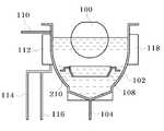
먼저 도 1을 참조하면, 배스(102) 내에 희석된 불산(HF)용액 및 과산화수소(H2O2)용액의 혼합용액을 공급한다. 배스(102)는 일정 부피의 액체를 담을 수 있는 용기 형태로서, 배스(102)의 하부 및 상부에는 각각 드레인라인(104) 및 덮개(106)가 배치된다. 배스(102) 내부에는 웨이퍼를 지지하기 위한 웨이퍼가이드(108)가 배치된다. 배스(102)의 측면에는 질소(N2) 또는 이소프로필알콜을 배스(102) 내부로 공급하는 노즐(110)이 배치된다. 또한 불산(HF)과 탈이온수(Deionized Water)를 배스(102) 내부로 공급하는 제1 공급장치(112)도 배치된다. 제1 공급장치(112)에는 불산(HF) 공급을 위한 제1 공급라인(114)과 탈이온수 공급을 위한 제2 공급라인(116)이 연결된다. 이 외에도 배스(102)의 측면에는 과산화수소(H2O2) 공급을 위한 제2 공급장치(118)가 배치된다.First, referring to FIG. 1, a mixed solution of a hydrofluoric acid (HF) solution and a hydrogen peroxide (H2 O2 ) solution diluted in the
희석된 불산(HF)용액 및 과산화수소(H2O2)용액으로 이루어지는 혼합용액(210)은 후속에서의 웨이퍼로딩에 의해 배스(102) 내로 로딩되는 웨이퍼가 혼합용 액(210)에 의해 완전히 담가질 정도의 충분한 양을 공급한다. 이 혼합용액(210)의 불산(HF) 및 과산화수소(H2O2) 공급액의 농도는 대략 49wt%:30wt%가 되도록 한다. 그리고 이 혼합용액(210)에 포함되는 불산(HF)과 탈이온수와 과산화수소(H2O2)의 부피비(volume ratio)는 대략 1:100 내지 300:0.05 내지 0.1이 되도록 한다. 또한 상기 혼합용액(210)의 온도는 대략 20 내지 30℃가 되도록 한다.The
다음에 도 2를 참조하면, 혼합용액(210)이 채워진 배스(102) 내에 웨이퍼(100)를 로딩한다. 웨이퍼(100)는 복수개가 하나의 세트로 구성되는 배치(batch) 형태로 배스(102) 내에 로딩될 수 있다. 이 웨이퍼(100)에는 금속을 포함하는 물질막(미도시)이 노출된다. 여기서 물질막은 금속막 또는 금속산화막이 포함될 수 있다. 예컨대 금속막으로서, 티타늄(Ti)막, 구리(Cu)막, 백금(Pt)막 또는 루테늄(Ru)막을 포함할 수 있으며, 금속산화막으로서, 알루미나(Al2O3), 하프늄산화막(HfO2), 지르콘산화(ZrO2)막, 탄탈륨산화(Ta2O5)막 또는 티타늄산화(TiO2)막을 포함할 수 있다.Next, referring to FIG. 2, the
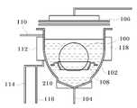
다음에 도 3을 참조하면, 웨이퍼(100)를 웨이퍼지지대(108)에 지지되도록 함으로써 웨이퍼(100)가 혼합용액(210) 내로 완전히 담가지도록 한다. 이 상태를 일정 시간동안 유지하여 웨이퍼(100)가 혼합용액(210)에 의해 린스(rinse)되도록 한다. 이 린스단계에서 웨이퍼(100) 상에 잔류하고 있는 산화막과 금속 또는 금속산화막의 찌꺼기는 제거된다. 경우에 따라서는 혼합용액(210)에 다른 세정액, 예컨대 SPM(Sulfuric acid peroxide mixture; H2SO4:H2O2:H2O), BOE(Buffered Oxide Etchant; NH4F:H2O:계면활성제) 및 SC-1(Standard Clean-1)로 이루어지는 세정액이 포함되도록 할 수 있다. 또는 이와 같은 세정액에 의해 1차로 세정을 한 후에 상기 혼합용액(210)만을 사용하여 최종 린스단계를 수행할 수도 있다.Next, referring to FIG. 3, the
다음에 도 4를 참조하면, 배스(102) 하부의 드레인라인(104)을 통해 혼합용액(210)을 배출시킨다. 그리고 배스(102) 내에 탈이온수(220)를 공급한다. 이 탈이온수(220)는 제2 공급라인(116)과 제1 공급장치(112)를 통해 배스(102) 내로 공급된다. 혼합용액(210)과 마찬가지로 탈이온수(220)도 또한 웨이퍼지지대(108)에 의해 지지되고 있는 웨이퍼(100)가 완전히 탈이온수(220)에 의해 담가질 정도의 양이 공급되도록 한다. 다음에 이 상태를 일정 시간동안 유지하여, 배스(102) 내의 탈이온수(220)에 의해 웨이퍼(100)가 린스되도록 한다.Next, referring to FIG. 4, the
다음에 도 5를 참조하면, 배스(102) 하부의 드레인라인(104)을 통해 탈이온수(220)를 배출시킨다. 이와 같이 탈이온수(220)의 배출이 끝나면, 혼합용액(210)에 의한 1차 최종린스와 탈이온수(220)에 의한 2차 최종린스가 끝나게 된다.Next, referring to FIG. 5, the
다음에 도 6을 참조하면, 노즐(110)을 통해 이소프로필알콜(IPA; IsoPropyl Alcohol) 증기(230)를 배스(102) 내로 공급한다.Next, referring to FIG. 6, an isopropyl alcohol (IPA)
다음에 도 7을 참조하면, 이소프로필알콜 증기(230)를 이용한 최종드라이단계를 수행한다. 즉 이소프로필알콜 증기(230)에 의해 웨이퍼(100) 표면의 물을 제거시킨다. 이소프로필알콜은 물과의 용해성이 높으며, 이에 따라 웨이퍼(100) 표면 의 수분은 빠르게 이소프로필알콜과 치환되며, 이에 따라 웨이퍼(100) 표면의 워터마크(water mark)를 유발하지 않고 웨이퍼(100)를 건조시킬 수 있다.Next, referring to FIG. 7, a final dry step using
지금까지 설명한 바와 같이, 본 발명에 따른 세정방법에 의하면, 희석된 불산(HF) 및 과산화수소(H2O2)로 이루어지는 혼합용액(210)에 의해 최종 린스단계를 수행함으로써 배스(102) 내의 금속 오염물이나 잔류물을 제거할 수 있다. 따라서 금속 또는 금속산화막을 포함하는 물질막이 노출된 웨이퍼(100)에 대한 세정공정을 수행한 후에도 동일한 배스(102)를 사용하여 다른 웨이퍼들에 대해 세정공정을 수행하더라도 웨이퍼에 대한 금속 오염이 발생되지 않는다.As described above, according to the cleaning method according to the present invention, the metal in the
일 예로서, 디램(DRAM)의 커패시터 상부전극에 대한 식각을 수행하는 경우, 층간절연막, 유전체막으로서의 알루미나(Al2O3) 및 상부전극이 순차적으로 식각되는데, 이 과정에서 알루미나(Al2O3)의 측면이 노출된다. 이 상태에서 기존의 SPM, BOE 및 SC-1만으로 세정하게 되는 경우, 알루미나(Al2O3)의 노출면에서 발생한 알루미늄(Al)에 의한 오염이 발생하는 반면에, 본원발명에서와 같이 희석된 불산(HF) 및 과산화수소(H2O2)로 이루어지는 혼합용액(210)에 의해 최종 린스단계를 수행하는 경우 알루미늄(Al)에 의한 오염이 방지된다. 이후에 다른 공정단계를 거친 웨이퍼, 예컨대 반도체기판의 불순물영역과 비트라인 또는 커패시터의 하부전극을 연결시키는 랜딩플러그컨택 형성을 위한 식각을 수행한 웨이퍼에 대해서 동일한 배스에서 세정공정을 수행하더라도 알루미늄(Al) 오염은 발생하지 않는다. 이는 막 증착 전에 이 루어지는 세정공정의 경우에도 마찬가지로 적용될 수 있다.For example, when etching the capacitor upper electrode of the DRAM, an interlayer insulating film, alumina (Al2 O3 ) as a dielectric film, and the upper electrode are sequentially etched, and in this process, alumina (Al2 O) is etched.3 ) the sides of the are exposed. In this state, when washing with only existing SPM, BOE and SC-1, contamination by aluminum (Al) generated on the exposed surface of alumina (Al2 O3 ) occurs, while diluted as in the present invention. When the final rinse step is performed by the
도 8은 본 발명에 따른 반도체웨이퍼의 세정방법에서 사용되는 세정액의 과산화수소 함량에 따른 구리 오염정도를 나타내 보인 그래프이다.8 is a graph showing the degree of copper contamination according to the hydrogen peroxide content of the cleaning liquid used in the method of cleaning a semiconductor wafer according to the present invention.
도 8을 참조하면, 구리(Cu)가 1ppm으로 오염된 불산(HF)용액에서 과산화수소(H2O2)를 첨가한 경우에, 첨가되는 과산화수소(H2O2)의 부피비에 따른 구리(Cu) 밀도를 측정한 결과, 도면에서 참조부호 "810"으로 나타낸 선과 같이, 과산화수소(H2O2) 첨가 없는 경우에 비하여, 도면에서 참조부호 "820"으로 나타낸 바와 같이 과산화수소(H2O2)를 첨가한 경우, 구리(Cu) 농도(concentration)가 감소한다는 것을 알 수 있다. 특히 과산화수소(H2O2)의 부피비가 증가할수록 구리(Cu) 농도는 현저하게 감소된다.Referring to FIG. 8, when hydrogen peroxide (H2 O2 ) is added to hydrofluoric acid (HF) solution in which copper (Cu) is contaminated with 1 ppm, copper (Cu) according to the volume ratio of hydrogen peroxide (H2 O2 ) added ) As a result of measuring the density, hydrogen peroxide (H2 O2 ), as indicated by
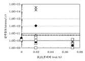
도 9는 본 발명에 따른 반도체웨이퍼의 세정방법에서 사용되는 세정액의 과산화수소 부피비에 따른 금속 오염정도를 나타내 보인 그래프이다.9 is a graph showing the degree of metal contamination according to the hydrogen peroxide volume ratio of the cleaning liquid used in the method for cleaning a semiconductor wafer according to the present invention.
도 9를 참조하면, 과산화수소(H2O2)의 부피비에 따른 금속 농도를 여러 금속에 따라 측정한 결과, 도면에서 참조부호 "◆"로 나타낸 바와 같이, 알루미늄(Al)의 경우 대략 0.03 이상의 부피비에서 허용가능농도(도면에서 점선으로 표시)인 5×10¹⁰atom/㎠ 이하로 측정되고 있다. 그리고 도면에서 참조부호 "□"로 나타낸 바와 같이, 철(Fe)의 경우에도 대략 0.03 이상의 부피비에서 허용가능농도(도면에서 점선으로 표시)인 5×10¹⁰atom/㎠ 이하로 측정되고 있다. 또한 도면에서 참조부호 " *"로 나타낸 바와 같이, 하프늄(Hf)의 경우에도 대략 0.03 이상의 부피비에서 허용가능농도(도면에서 점선으로 표시)인 5×10¹⁰atom/㎠ 이하로 측정되고 있다. 이와 같은 결과를 종합해보면 대략 0.05 이상의 부피비에서는 금속 농도를 허용가능농도 이하로 유지할 수 있으며, 이에 따라 대략 0.05 이상의 부피비의 과산화수소(H2O2)의 추가로 인하여 금속 오염의 방지를 최대화할 수 있다는 것을 알 수 있다.Referring to FIG. 9, as a result of measuring the metal concentration according to the volume ratio of hydrogen peroxide (H2 O2 ) according to various metals, as shown by reference numeral “◆” in the drawing, in the case of aluminum (Al), the volume ratio of about 0.03 or more It is measured at 5 × 10¹⁰ atom / cm 2 or less, which is the allowable concentration (indicated by the dotted line in the figure). In addition, as indicated by the reference numeral “□” in the drawings, iron (Fe) is also measured at an allowable concentration (denoted by a dotted line in the drawing) of 5 × 10¹⁰ atom / cm 2 or less at a volume ratio of about 0.03 or more. In addition, as indicated by the reference numeral "*" in the drawings, even in the case of hafnium (Hf), it is measured at 5 × 10¹⁰ atom / cm 2 or less, which is an allowable concentration (indicated by a dotted line in the figure) at a volume ratio of approximately 0.03 or more. Taken together, these results can maintain the metal concentration below the allowable concentration at a volume ratio of approximately 0.05 or more, thus maximizing the prevention of metal contamination due to the addition of hydrogen peroxide (H2 O2 ) of approximately 0.05 or more. It can be seen that.
지금까지 설명한 바와 같이, 본 발명에 따른 반도체웨이퍼의 세정방법에 의하면, 희석된 불산(HF) 및 과산화수소(H2O2)가 혼합된 혼합용액을 이용한 최종린스단계를 수행함으로써, 금속 오염물 발생원인이 노출된 웨이퍼에 대한 세정공정을 수행하더라도 금속 오염이 발생하지 않으며, 이에 따라 세정설비를 다른 여러 공정에서 사용하더라도 금속 오염에 의한 수율저하를 억제할 수 있을 뿐만 아니라, 금속 불순물에 의한 막질 사이의 계면에서의 특성 저하를 방지할 수 있다는 이점들이 제공된다.As described so far, according to the method of cleaning a semiconductor wafer according to the present invention, by performing a final rinse step using a mixed solution of diluted hydrofluoric acid (HF) and hydrogen peroxide (H2 O2 ), the cause of the generation of metal contaminants Even if the cleaning process is performed on the exposed wafers, metal contamination does not occur. Accordingly, even if the cleaning equipment is used in other processes, the yield reduction due to metal contamination can be suppressed and the film quality caused by metal impurities can be reduced. Advantages are provided that the degradation of properties at the interface can be prevented.
이상 본 발명을 바람직한 실시예를 들어 상세하게 설명하였으나, 본 발명은 상기 실시예에 한정되지 않으며, 본 발명의 기술적 사상 내에서 당 분야에서 통상의 지식을 가진 자에 의하여 여러 가지 변형이 가능함은 당연하다.Although the present invention has been described in detail with reference to preferred embodiments, the present invention is not limited to the above embodiments, and various modifications may be made by those skilled in the art within the technical spirit of the present invention. Do.
Claims (15)
Translated fromKoreanPriority Applications (2)
| Application Number | Priority Date | Filing Date | Title |
|---|---|---|---|
| KR1020050028294AKR20070087702A (en) | 2005-04-04 | 2005-04-04 | Cleaning method of semiconductor wafers to suppress metal contamination |
| US11/288,481US20060219259A1 (en) | 2005-04-04 | 2005-11-29 | Method of cleaning a semiconductor wafer |
Applications Claiming Priority (1)
| Application Number | Priority Date | Filing Date | Title |
|---|---|---|---|
| KR1020050028294AKR20070087702A (en) | 2005-04-04 | 2005-04-04 | Cleaning method of semiconductor wafers to suppress metal contamination |
Publications (1)
| Publication Number | Publication Date |
|---|---|
| KR20070087702Atrue KR20070087702A (en) | 2007-08-29 |
Family
ID=37068865
Family Applications (1)
| Application Number | Title | Priority Date | Filing Date |
|---|---|---|---|
| KR1020050028294ACeasedKR20070087702A (en) | 2005-04-04 | 2005-04-04 | Cleaning method of semiconductor wafers to suppress metal contamination |
Country Status (2)
| Country | Link |
|---|---|
| US (1) | US20060219259A1 (en) |
| KR (1) | KR20070087702A (en) |
Families Citing this family (4)
| Publication number | Priority date | Publication date | Assignee | Title |
|---|---|---|---|---|
| ATE498831T1 (en)* | 2006-09-25 | 2011-03-15 | Grundfos Management As | SEMICONDUCTOR COMPONENT |
| JP6139890B2 (en)* | 2013-01-18 | 2017-05-31 | 株式会社東芝 | Semiconductor device manufacturing method and semiconductor manufacturing apparatus |
| JP2017119234A (en)* | 2015-12-28 | 2017-07-06 | ダウ グローバル テクノロジーズ エルエルシー | Process for refining hydrophilic organic solvent |
| CN112103179B (en)* | 2020-11-03 | 2021-03-02 | 晶芯成(北京)科技有限公司 | Manufacturing method of MIM capacitor |
Family Cites Families (9)
| Publication number | Priority date | Publication date | Assignee | Title |
|---|---|---|---|---|
| US5498293A (en)* | 1994-06-23 | 1996-03-12 | Mallinckrodt Baker, Inc. | Cleaning wafer substrates of metal contamination while maintaining wafer smoothness |
| US5989353A (en)* | 1996-10-11 | 1999-11-23 | Mallinckrodt Baker, Inc. | Cleaning wafer substrates of metal contamination while maintaining wafer smoothness |
| JPH10144650A (en)* | 1996-11-11 | 1998-05-29 | Mitsubishi Electric Corp | Semiconductor material cleaning equipment |
| TW426874B (en)* | 1998-10-14 | 2001-03-21 | United Microelectronics Corp | Method for cleaning a semiconductor wafer |
| TW580736B (en)* | 2000-04-27 | 2004-03-21 | Hitachi Ltd | Fabrication method for semiconductor device |
| JP2002261062A (en)* | 2001-03-05 | 2002-09-13 | Texas Instr Japan Ltd | Method and apparatus for removing particles on a semiconductor wafer |
| TW508681B (en)* | 2001-05-11 | 2002-11-01 | Macronix Int Co Ltd | Cleaning method of semiconductor manufacture process for preventing metal corrosion |
| US6585826B2 (en)* | 2001-11-02 | 2003-07-01 | Taiwan Semiconductor Manufacturing Co., Ltd | Semiconductor wafer cleaning method to remove residual contamination including metal nitride particles |
| TW508691B (en)* | 2001-12-21 | 2002-11-01 | Nanya Technology Corp | Cleaning method after etching metal layer |
- 2005
- 2005-04-04KRKR1020050028294Apatent/KR20070087702A/ennot_activeCeased
- 2005-11-29USUS11/288,481patent/US20060219259A1/ennot_activeAbandoned
Also Published As
| Publication number | Publication date |
|---|---|
| US20060219259A1 (en) | 2006-10-05 |
Similar Documents
| Publication | Publication Date | Title |
|---|---|---|
| US10559651B2 (en) | Method of forming memory capacitor | |
| KR20050110470A (en) | Composition for cleaning a semiconductor substrate, method for cleaning a semiconductor substrate and method for manufacturing a semiconductor device using the same | |
| KR100505675B1 (en) | Method for manufacturing capacitor with multi-stepped wet treatment to surface of electrode | |
| JP3679216B2 (en) | Semiconductor substrate cleaning liquid and cleaning method using the same | |
| JP2001237389A (en) | Method for manufacturing semiconductor device | |
| JP7195084B2 (en) | Substrate processing method and substrate processing apparatus | |
| JPH09275085A (en) | Semiconductor substrate cleaning method, cleaning apparatus, semiconductor substrate manufacturing film forming method, and film forming apparatus | |
| TW200408060A (en) | Method for forming ruthenium storage node of semiconductor device | |
| KR20070087702A (en) | Cleaning method of semiconductor wafers to suppress metal contamination | |
| KR100808597B1 (en) | MIM capacitor formation method | |
| CN101213644A (en) | Methods of etching oxide, reducing roughness, and forming capacitor structures | |
| Choi | Necessity of cleaning and its application in future memory devices | |
| KR100771535B1 (en) | Rinsing Method of Semiconductor Wafers for Metal Pollution Suppression | |
| KR100818089B1 (en) | Manufacturing method of semiconductor device | |
| US9394509B2 (en) | Cleaning solution composition and method of cleaning semiconductor device using the same | |
| KR100666380B1 (en) | A photoresist removal method and a method of manufacturing a semiconductor device using the same. | |
| KR101185989B1 (en) | Method of fabricating storage node in semiconductor device | |
| JPH09190994A (en) | Deionizing water/ozone cleanig after hydrofluoric acid treatment for prevention of creation of residue of silicic acid | |
| JP2003332465A (en) | Method for manufacturing semiconductor memory device | |
| KR20230093245A (en) | Amine oxides for etching, stripping and cleaning applications | |
| KR100613455B1 (en) | Manufacturing method of semiconductor device | |
| KR101045375B1 (en) | Method of Cleaning Semiconductor Devices | |
| KR100495653B1 (en) | Process for clearing an wafer | |
| CN105448652B (en) | The cleaning procedure of contact groove and the forming method of contact layer | |
| KR19990005869A (en) | Wafer cleaning method |
Legal Events
| Date | Code | Title | Description |
|---|---|---|---|
| A201 | Request for examination | ||
| PA0109 | Patent application | Patent event code:PA01091R01D Comment text:Patent Application Patent event date:20050404 | |
| PA0201 | Request for examination | ||
| E902 | Notification of reason for refusal | ||
| PE0902 | Notice of grounds for rejection | Comment text:Notification of reason for refusal Patent event date:20060427 Patent event code:PE09021S01D | |
| E601 | Decision to refuse application | ||
| PE0601 | Decision on rejection of patent | Patent event date:20060828 Comment text:Decision to Refuse Application Patent event code:PE06012S01D Patent event date:20060427 Comment text:Notification of reason for refusal Patent event code:PE06011S01I | |
| J201 | Request for trial against refusal decision | ||
| PJ0201 | Trial against decision of rejection | Patent event date:20060922 Comment text:Request for Trial against Decision on Refusal Patent event code:PJ02012R01D Patent event date:20060828 Comment text:Decision to Refuse Application Patent event code:PJ02011S01I Appeal kind category:Appeal against decision to decline refusal Decision date:20070914 Appeal identifier:2006101008489 Request date:20060922 | |
| PG1501 | Laying open of application | ||
| J301 | Trial decision | Free format text:TRIAL DECISION FOR APPEAL AGAINST DECISION TO DECLINE REFUSAL REQUESTED 20060922 Effective date:20070914 | |
| PJ1301 | Trial decision | Patent event code:PJ13011S01D Patent event date:20070918 Comment text:Trial Decision on Objection to Decision on Refusal Appeal kind category:Appeal against decision to decline refusal Request date:20060922 Decision date:20070914 Appeal identifier:2006101008489 |