KR20070078372A - Systems and methods for inspecting patterned devices with microconductors - Google Patents
Systems and methods for inspecting patterned devices with microconductorsDownload PDFInfo
- Publication number
- KR20070078372A KR20070078372AKR1020070004118AKR20070004118AKR20070078372AKR 20070078372 AKR20070078372 AKR 20070078372AKR 1020070004118 AKR1020070004118 AKR 1020070004118AKR 20070004118 AKR20070004118 AKR 20070004118AKR 20070078372 AKR20070078372 AKR 20070078372A
- Authority
- KR
- South Korea
- Prior art keywords
- illumination
- defect
- defects
- camera
- images
- Prior art date
- Legal status (The legal status is an assumption and is not a legal conclusion. Google has not performed a legal analysis and makes no representation as to the accuracy of the status listed.)
- Granted
Links
Images


Classifications
- G—PHYSICS
- G01—MEASURING; TESTING
- G01N—INVESTIGATING OR ANALYSING MATERIALS BY DETERMINING THEIR CHEMICAL OR PHYSICAL PROPERTIES
- G01N21/00—Investigating or analysing materials by the use of optical means, i.e. using sub-millimetre waves, infrared, visible or ultraviolet light
- G01N21/84—Systems specially adapted for particular applications
- G01N21/88—Investigating the presence of flaws or contamination
- G01N21/95—Investigating the presence of flaws or contamination characterised by the material or shape of the object to be examined
- G01N21/956—Inspecting patterns on the surface of objects
- B—PERFORMING OPERATIONS; TRANSPORTING
- B22—CASTING; POWDER METALLURGY
- B22C—FOUNDRY MOULDING
- B22C9/00—Moulds or cores; Moulding processes
- B22C9/08—Features with respect to supply of molten metal, e.g. ingates, circular gates, skim gates
- B22C9/082—Sprues, pouring cups
Landscapes
- General Health & Medical Sciences (AREA)
- General Physics & Mathematics (AREA)
- Physics & Mathematics (AREA)
- Health & Medical Sciences (AREA)
- Life Sciences & Earth Sciences (AREA)
- Chemical & Material Sciences (AREA)
- Analytical Chemistry (AREA)
- Biochemistry (AREA)
- Pathology (AREA)
- Immunology (AREA)
- Engineering & Computer Science (AREA)
- Mechanical Engineering (AREA)
- Investigating Materials By The Use Of Optical Means Adapted For Particular Applications (AREA)
- Length Measuring Devices By Optical Means (AREA)
- Testing Of Optical Devices Or Fibers (AREA)
- Image Processing (AREA)
- Image Analysis (AREA)
Abstract
Description
Translated fromKorean도 1A는 전기 전도체와 같은 복수의 신축 소자들을 포함하는 디스플레이 패널의 일부에 대한 도면이며, 결함의 유형을 다양하게 나타낸다. 여기서, 디스플레이 패널이 제 1 조명 모드에서 다색, 다방향 검사 프로세스 동작을 사용하여 검사된다.FIG. 1A is a diagram of a portion of a display panel that includes a plurality of stretchable elements, such as electrical conductors, and illustrates various types of defects. Here, the display panel is inspected using a multicolor, multidirectional inspection process operation in the first illumination mode.
도 1B는 도 1A의 디스플레이 패널을 나타내는 도면으로, 여기서 디스플레이 패널은 제 2 조명 모드에서 동작하는 도 1A의 다색, 다방향 조사 프로세스를 사용하여 검사된다.FIG. 1B illustrates the display panel of FIG. 1A, wherein the display panel is inspected using the multicolor, multidirectional irradiation process of FIG. 1A operating in a second illumination mode. FIG.
도 2는 도 1A 및 1B에 각각 도시된 두 개의 선택가능한 조명 모드에서 조명을 제공하는 본 발명의 바람직한 실시예에 따라 구성되고 동작하는 조명기를 나타낸다.FIG. 2 shows an illuminator constructed and operative in accordance with a preferred embodiment of the present invention for providing illumination in two selectable illumination modes shown in FIGS. 1A and 1B, respectively.
도 3A-3C는 도 2에 도시된 조명기의 측면, 끝단 그리고 바닥 형상을 각각 나타낸다.3A-3C show the side, end and bottom shapes of the illuminator shown in FIG. 2, respectively.
도 4A는 제 1 조명 모드에서 동작하는 도 2-3C에 도시된 조명기와 조명 광선을 나타내는 도면이다.4A shows the illuminator and illumination rays shown in FIGS. 2-3C operating in a first illumination mode.
도 4B는 제 2 조명 모드에서 동작하는 도 2-3C에 도시된 조명기와 조명 광선 을 나타내는 도면이다.4B shows the illuminator and illumination rays shown in FIGS. 2-3C operating in the second illumination mode.
도 4C는 도 2-3C에 도시된 조명기에 의해 제공되는 광축으로부터 이동된 조명에 대한 각 방향 원점을 나타내는 개략도이다.4C is a schematic diagram illustrating the directional origin in each direction for illumination moved from the optical axis provided by the illuminator shown in FIGS. 2-3C.
도 4D는 입사 조명 빔과 광축 사이의 각도에 대한 함수로써 에지 밝기에 대한 먼지 조명 응답의 명도 사이의 비를 점으로 나타내는 그래프이다.FIG. 4D is a graph plotting the ratio between the brightness of the dust illumination response to edge brightness as a function of the angle between the incident illumination beam and the optical axis.
도 4E는 삼색이 사용되는, 비 방향성 결함으로부터 방향성 결함을 구분하는데 유용한 제 1 다방향 조명 모드를 나타내는 개략도이다.4E is a schematic diagram illustrating a first multidirectional illumination mode useful for distinguishing directional defects from non-directional defects in which three colors are used.
도 4F는 삼색이 사용되는, 비 방향성 결함으로부터 방향성 결함을 구분하는데 유용한 제 2 다방향 조명 모드를 나타내는 개략도이다.4F is a schematic diagram illustrating a second multidirectional illumination mode useful for distinguishing directional defects from non-directional defects in which three colors are used.
도 4G는 도시된 두 개의 조명 모드 각각에서, 각 후보 결함의 두 개의 이미지를 획득하고 비교하여 비 방향성 결함으로부터 방향성 결함을 구분하는 데 유용한 한 쌍의 조명 모드를 나타내는 개략도이다.4G is a schematic diagram illustrating a pair of illumination modes useful for distinguishing directional defects from non-directional defects by obtaining and comparing two images of each candidate defect in each of the two illumination modes shown.
도 5A는 도 1A 및 1B에 각각 도시된 제 1 및 제 2 조명 모드에서, 수직방향 절단이되거나 절단이 되지 않은, 다양한 원점을 가지는 복수의 신축 소자의 외형을 나타내는 표이다.5A is a table showing the appearance of a plurality of telescopic elements having various origins, with or without vertical cutting, in the first and second illumination modes shown in FIGS. 1A and 1B, respectively.
도 5B는 도 1A 및 1B에 각각 도시된 제 1 및 제 2 조명 모드에서, 다양한 종류의 먼지-전기 전도체 구조의 외형을 나타내는 표이다.5B is a table showing the appearance of various kinds of dust-electric conductor structures in the first and second illumination modes shown in FIGS. 1A and 1B, respectively.
도 7A는 도 2에 도시된 조명기를 포함하는 본 발명의 바람직한 실시예에 따라 구성되고 동작하는 스캐닝 및 비디오 검증 시스템에 장착된 워크피스를 나타내는 조감도이다.FIG. 7A is a bird's eye view of a workpiece mounted in a scanning and video verification system constructed and operative in accordance with a preferred embodiment of the present invention including the illuminator shown in FIG.
도 7B는 워크피스가 제거된 도 7A에 도시된 스캐닝 및 비디오 검증 시스템을 나타내는 조감도이다.FIG. 7B is a bird's eye view of the scanning and video verification system shown in FIG. 7A with the workpiece removed. FIG.
도 8은 다양한 덮개가 제거된 도 7A-7B에 도시된 광학 헤드의 확대도이다.8 is an enlarged view of the optical head shown in FIGS. 7A-7B with various covers removed.
도 9는 도 7A-7B의 검증 카메라 서브시스템을 나타내는 측면도이다.9 are side views illustrating the verification camera subsystem of FIGS. 7A-7B.
도 10은 미세 구조를 가지는 워크피스 내의 후보 결함을 방향성 있게 조명하는 자동 광 검사 시스템을 나타내는 개략적인 기능 블록도이다.10 is a schematic functional block diagram illustrating an automated light inspection system that directionally illuminates candidate defects in a workpiece having a microstructure.
도 11은 도 10에 도시된 시스템의 바람직한 동작 방법을 나타내는 개략적인 흐름도이다.FIG. 11 is a schematic flowchart illustrating a preferred method of operation of the system shown in FIG. 10.
도 12는 도 10의 서브 시스템을 처리하는 방향 정보를 설정하는 바람직한 방법을 나타내는 개략적인 흐름도이다.12 is a schematic flowchart illustrating a preferred method of setting direction information for processing the subsystem of FIG. 10.
본 발명은 제조된 대상 상의 미세 구조에 대한 광범위한 검사에 관한 것이다.The present invention relates to extensive inspection of the microstructures on the subjects produced.
제조 중인 평판 디스플레의 결함을 검사하기 위한 자동 광 검사 시스템(이스라엘 야브네에 위치한 오보텍 사(Orbotech Ltd)로부터 상업적으로 사용되는 SuperVisionTM과, InVsionTM 시스템 포함한다)은 전형적으로 추정 결함의 이미지를 획득하도록 동작하는 결함 분류 서브 시스템(defect classification sub-system)을 포함한다. 추정 결함은 폴리크로마틱 또는 모노크로마틱 명시야 조명(bright field illumination)을 사용하여 조명된다.Automated light inspection systems (including SuperVision™ and InVsion™ systems commercially available from Orbotech Ltd, Israel Yavne) for inspecting defects in flat panel displays under construction typically acquire images of putative defects. And a defect classification sub-system operative to operate. Presumptive defects are illuminated using polychromatic or monochromatic bright field illumination.
제작 중인 평판 디스플레이의 결함을 검사하기 위한 일부 자동 광 검사 시스템(예를 들면, 이스라엘 야브네에 위치한 오보텍 사로부터 생산된 광학 테스터의 Pointer-5000 시리즈)이 추가로 이미지를 획득한다. 이미지는 광축으부터 이동된 위치로부터 공급되는 단일색 조명에 의해 조명된다.Some automated light inspection systems (for example, the Pointer-5000 series of optical testers produced by Obotech, based in Yavne, Israel) to check for defects in flat panel displays under construction acquire additional images. The image is illuminated by monochromatic illumination supplied from a position moved from the optical axis.
미국 특허 제6,947,151호는 서로 다른 색의 빛을 포함하는 조명을 사용하는 표면 상태 검사 방법 및 기판 검사 장치에 대해 기술한다. 여기서 서로 다른 색의 빛은 검사 대상에 대해 서로 다른 수직방향 각도를 가지는 복수의 방향으로 비추어진다.U. S. Patent No. 6,947, 151 describes a surface condition inspection method and a substrate inspection apparatus using illumination including light of different colors. The light of different colors is emitted in a plurality of directions having different vertical angles with respect to the inspection object.
위의 명세서에서 언급된 모든 출판물들과 직간접적으로 명세서에 인용된 출판물의 공개 물이 여기에 참조문헌으로 포함된다.All publications mentioned in the above specification and publications cited in the specification, directly or indirectly, are hereby incorporated by reference.
본 발명은 디스플레이 패널과 같은 제조 대상물 상에 미세 구조를 검사하는 향상된 시스템 및 방법을 제공하기 위한 것이다.It is an object of the present invention to provide an improved system and method for inspecting microstructure on an object of manufacture, such as a display panel.
본 발명의 시스템에 대한 하나의 실시예는 FPD(flat panel display) 패널 상의 절단 및 먼지 결함들을 구별하기 위한 것이다. 양쪽 유형의 결함들이 모두 명 영역 조명에서 암점(dark spot)으로 나타나고 암 영역 조명에서는 밝게 보인다. 먼지 결함은 조명 방향에 독립적으로 밝게 나타나므로, 본 발명의 바람직한 실시예는 조명의 방위 각에 매우 민감한 절단 밝기(cut brightness)를 분석함으로써 절단 및 먼지 결함들을 구별한다. 바람직하게는, 패널이 다양한 색에 의해 복수의 방향으로부터 동시에 조명되고, 이로써 가시화 및 외관상 결함의 성질에 대한 기계적 분석을 용이하게 하고 검사 시간을 가능한 짧게 한다. 패널의 다 방향, 다중 스펙트럼 조명의 결과로써, 절단 결함이 그 위치(방향성)에 강하게 의존하는 하나의 특정 색을 가진다. 반면에, 먼지 결함은 상대된 색을 가지는 두 개의 색을 가지는 것으로 나타낸다. 획득된 색 이미지는 각 색에 대하여 구체적으로 추가 분석될 수 있다.One embodiment of the system of the present invention is to distinguish cutting and dust defects on a flat panel display panel. Both types of defects appear as dark spots in bright area lighting and bright in dark area lighting. Since dust defects appear bright independent of the illumination direction, a preferred embodiment of the present invention distinguishes between cutting and dust defects by analyzing cut brightness which is very sensitive to the azimuth angle of the illumination. Preferably, the panel is illuminated simultaneously from a plurality of directions by various colors, thereby facilitating mechanical analysis of the properties of the visualization and appearance defects and making the inspection time as short as possible. As a result of the multi-directional, multi-spectral illumination of the panel, the cutting defect has one specific color that strongly depends on its position (directionality). Dust defects, on the other hand, are represented as having two colors with relative colors. The obtained color image may be further analyzed for each color in detail.
본 발명의 바람직한 실시예는 FPD 패널상에 관찰되는 결함의 서로 다른 유형들의 분류를 개선되도록 하며, 더욱 구체적으로 절단 및 먼지 결함들을 구별하도록 한다. FPD 제작중에, 많은 활성 막들이 하나의 유리 평판 상에 형성될 수 있다. 결함 유형을 식별하는 능력이 생산 라인 내의 문제를 표시할 수 있다. 본 발명의 시스템의 출력은 생산 라인이 적절히 고정되도록 함으로써 수율을 향상시킨다.Preferred embodiments of the present invention allow for improved classification of different types of defects observed on FPD panels, and more specifically to distinguish between cutting and dust defects. During FPD fabrication, many active films can be formed on one glass plate. The ability to identify the defect type can indicate a problem in the production line. The output of the system of the present invention improves yield by allowing the production line to be properly fixed.
본 발명의 바람직한 실시예에 따르면, DF(dark field) 조명방법이 사용되며, 다색 조명 장치를 사용하여 절단 및 먼지 결함들을 구별한다. 강한 빛의 산란 때문에, 양쪽 유형의 결함이 일반적인 명 영역 조명에서 암점으로 나타나며, 일반적인 암 영역 조명에서 밝게 나타난다. 조명 방법은 절단 및 먼지 결함들을 구분하는데 유용한데, 왜냐하면 절단 밝기가 조명의 방위각 방향에 매우 민감한 (방위각 방향은 x-y 평면상의 방향이다) 반면에, 먼지 결함은 조명 방향에 독립적으로 밝게 보이기 때문이다.According to a preferred embodiment of the present invention, a dark field (DF) illumination method is used, and a multicolor illumination device is used to distinguish cutting and dust defects. Due to the strong light scattering, both types of defects appear as dark spots in normal bright area illumination and bright in normal dark area illumination. The illumination method is useful for distinguishing between cutting and dust defects because the cutting brightness is very sensitive to the azimuthal direction of the illumination (the azimuth direction is the direction on the x-y plane), while the dust defects appear bright independently of the lighting direction.
바람직하게는, 패널이 다양한 색에 의해 여러 방향으로부터 동시에 조명된 다. 서로 다른 색은 서로 다른 방위각 방향에 연관되며, 이는 결함 성질의 가시화 및 자동 분류, 그리고 검사 시간 단축을 용이하게 한다. 결과적으로, 단축 결함은 방향성(위치)에 강하게 의존하는 주요 색을 가지며, 반면에 먼지 결함은, 작업자(사람)에 의해 또는 기계 분석시에 구별 및 인식하도록 하는 바와 같이 바람직하게 사용되는 두 색 또는 모든 색들 혼합 또는 복합 색으로 나타난다. 보다 컴퓨터화된 분석을 위해 결과 색 영상이 대응하는 1색 그림으로 분해될 수 있다. FPD 패널이 일반적으로 알려진 라인 위치(예, 방향에 있어서: 0도, 90도, 45도 및 135도)를 포함하며, 조명기는 전형적으로 두 그룹의 조명기 유닛(예, 워크피스의 알려진 라인 위치에 평행하게 배치된 발광 다이오나 광 섬유) 또는 모든 가능한 각도를 커버하기 위한 패널(예, 0도 및 90도 축과 45도 및 135도 축을 따라)을 포함한다.Preferably, the panels are illuminated simultaneously from different directions by various colors. Different colors are associated with different azimuth directions, which facilitates the visualization and automatic classification of defect properties and shortens inspection time. As a result, the uniaxial defects have a primary color strongly dependent on the orientation (position), while the dust defects are preferably two colors that are preferably used as distinguished and recognized by the operator (person) or during machine analysis. All colors appear as a mixed or complex color. For more computerized analysis, the resulting color image can be decomposed into a corresponding one-color picture. FPD panels generally include a known line position (eg, 0 degrees, 90 degrees, 45 degrees, and 135 degrees in direction), and the illuminator typically has two groups of illuminator units (eg, known line positions of the workpiece). Light emitting diodes or optical fibers arranged in parallel) or panels for covering all possible angles (eg, along the 0 and 90 degree axes and the 45 and 135 degree axes).
모든 정보가 하나의 셀에 대한 이미지로부터 추출되는 경우에 이웃하는 셀들 사이의 비교가 가능하면, 본 발명의 방법은 특히 큰 셀 디스플레이(TV-패널)의 스캐닝에 유용하다.The method of the invention is particularly useful for the scanning of large cell displays (TV-panels) if a comparison between neighboring cells is possible when all the information is extracted from an image for one cell.
본 발명의 시스템 및 방법은 평판 디스플레이의 자동 광 검사에 특히 유용하다.The systems and methods of the present invention are particularly useful for automatic light inspection of flat panel displays.
본 발명의 바람직한 실시예에 따르면, 미세 전도체를 가지는 패터닝된 장치를 검사하는 검사 시스템에 있어서, 상기 시스템은: 평면을 정의하는 패터닝된 기판상의 후보 결함 위치를 보여주는 카메라로써, 상기 위치에 대한 하나 이상의 이미지를 획득하며, 상기 카메라는 광축을 정의하고, 상기 하나 이상의 이미지는 상기 광축으로부터 오프셋 된 하나 이상의 광원으로부터의 조명에 의해 조명되며, 상 기 조명은 상기 평면에 대응하는 평면에 서로 평행하지 않은 하나 이상의 제 1 및 제 2 경로를 따라 제공되고, 여기서 상기 제 1 조명 경로를 따라 제공되는 조명에 대한 응답이 상기 제 2 조명 경로를 따라 제공되는 조명에 대한 응답과 구별되는 상기 카메라와; 그리고 상기 하나 이상의 이미지를 입력받아, 다른 유형의 후보 결함들로부터 상기 패터닝된 기판에 대한 외부 입자에 의해 야기되는 후보 결함을 구별하는 결함 분류기를 포함한다.According to a preferred embodiment of the present invention, an inspection system for inspecting a patterned device having microconductors, the system comprising: a camera showing candidate defect locations on a patterned substrate that define a plane, the one or more locations of which Obtaining an image, the camera defining an optical axis, the one or more images being illuminated by illumination from one or more light sources offset from the optical axis, the illumination being one not parallel to each other in a plane corresponding to the plane The camera provided along the first and second paths above, wherein a response to illumination provided along the first illumination path is distinct from a response to illumination provided along the second illumination path; And a defect classifier that receives the one or more images and distinguishes candidate defects caused by foreign particles to the patterned substrate from other types of candidate defects.
또한, 본 발명의 다른 바람직한 실시예에 따르면, 미세 전도체를 가지는 패터닝된 장치를 검사하는 검사 방법에 있어서, 상기 방법은: 평면을 정의하는 패터닝된 기판상에 후보 입자의 위치를 보여주고, 상기 위치의 하나 이상의 이미지를 획득하는 단계로서, 카메라가 광축을 정의하는 상기 단계와; 상기 광축으로부터 오프셋 된 하나 이상의 광원으로부터의 조명을 사용하여 상기 하나 이상의 이미지를 조명하는 단계로서, 상기 조명은 상기 평면에 대응하는 평면에서 상호 평행하지 않은 하나 이상의 제 1 및 제 2 조명 경로들을 따라 공급되고, 상기 제 1 조명 경로를 따라 공급되는 조명에 대한 응답이 상기 제 2 조명 경로를 따라 공급되는 조명에 대한 응답과 구별되는 상기 조명 단계와; 그리고 상기 하나 이상의 이미지를 분석하여, 상기 패터닝된 기판에 대한 외부 입자에 의해 야기된 후보 결함과 다른 유형의 후보 결함들을 구별하는 단계를 포함한다.In addition, according to another preferred embodiment of the present invention, in a test method for inspecting a patterned device having a microconductor, the method comprises: showing a position of a candidate particle on a patterned substrate defining a plane, said position Obtaining one or more images of the camera, the camera defining an optical axis; Illuminating the one or more images using illumination from one or more light sources offset from the optical axis, the illumination being supplied along one or more first and second illumination paths that are not parallel to each other in a plane corresponding to the plane The illumination step wherein the response to illumination supplied along the first illumination path is distinct from the response to illumination supplied along the second illumination path; And analyzing the one or more images to distinguish candidate defects from other types of candidate defects caused by foreign particles to the patterned substrate.
또한, 본 발명의 또 다른 바람직한 실시예에 따르면, 미세 전도체를 가지는 전기 광학 장치를 검사하는 자동 검사 시스템에 있어서, 상기 시스템은: 대응하는 복수의 결함 위치들의 복수의 암 영역 조명으로 조명된 이미지를 획득하고, 절단과 같은 방향성 결함과 입자와 같은 비 방향성 결함을 구별하는 이에 대응하는 복수의 대응 출력들을 발생하는 결함 분류기를 포함한다. 바람직하게는, 다중 암 영역 조명이 사용된다.Further, according to another preferred embodiment of the present invention, in an automatic inspection system for inspecting an electro-optical device having a microconductor, the system includes: illuminating an image illuminated with a plurality of dark area illuminations of a corresponding plurality of defect locations. A defect classifier that obtains and generates a plurality of corresponding outputs corresponding thereto that distinguish directional defects such as cutting and non-directional defects such as particles. Preferably, multiple dark area illumination is used.
나아가, 본 발명의 또 다른 바람직한 실시예에서, 상기 복수의 출력은 암 영역 조명으로 조명된 이미지들을 포함한다.Furthermore, in another preferred embodiment of the present invention, the plurality of outputs comprise images illuminated with dark area illumination.
본 발명의 또 다른 바람직한 실시예에서, 복수의 출력들은 개별적인 복수의 결함 위치들의 개별적인 복수의 분류를 포함하고, 하나 이상의 분류는 방향성 결함 카테고리이고 다른 하나 이상의 분류는 비 방향성 결함 카테고리이다.In another preferred embodiment of the present invention, the plurality of outputs comprises an individual plurality of classifications of individual plurality of defect locations, one or more classifications being a directional defect category and the other one or more classifications being a non-directional defect category.
나아가 본 발명의 또 다른 바람직한 실시예에서, 상기 이미지들은 다 방향성으로 조명된다.Furthermore in another preferred embodiment of the present invention the images are illuminated in a multi-directional manner.
본 발명의 또 다른 바람직한 실시예에서, 상기 이미지들은 다중 스펙트럼으로 조명된다.In another preferred embodiment of the invention, the images are illuminated in multiple spectra.
또한, 본 발명의 또 다른 바람직한 실시예에서, 상기 이미지들은 동일한 광학 특성이 있는 반면에 시간에 의해 구분되는 서로 다른 방향으로부터의 방향성 조명에 의해 조명된다.Furthermore, in another preferred embodiment of the invention, the images are illuminated by directional illumination from different directions separated by time while having the same optical properties.
또한, 본 발명의 다른 바람직한 실시예에 따르면, 미세 구조를 가지는 제조된 대상물의 자동 광 검사를 위한 방법에서, 상기 방법은 제작된 대상의 결함을 검증하기 위한 다중 스펨트럼 다중 각도 암 영역 이미지를 사용하는 단계를 포함한다.Further, according to another preferred embodiment of the present invention, in a method for automatic light inspection of a manufactured object having a microstructure, the method uses a multi-spectrum multi-angle arm area image for verifying a defect of the manufactured object. It includes a step.
나아가, 본 발명의 또 다른 바람직한 실시예에서, 상기 제작된 대상은 평판 디스플레이를 포함한다.Furthermore, in another preferred embodiment of the present invention, the manufactured object comprises a flat panel display.
또한, 본 발명의 다른 바람직한 실시예에 따르면, 미세 구조를 가지는 제작된 대상물을 검사하는 자동 검사 시스템이 제공되며, 상기 시스템은 미세 구조를 가지는 제작된 대상의 일부 이상의 이미지화하는 광학 헤드와, 검사될 제작 대상물과 광학 헤드 사이의 상대적인 이동을 제공하는 상대 동작 제공기를 포함하되, 상기 광학 헤드는 복수의 방향으로부터의 조명을 제공하는 다 방향 조명기를 포함하고, 상기 다 방향 조명기는 복수의 개별적인 방향으로부터의 조명을 제공하는 복수의 서로 다른 색 조명 원을 포함한다.Further, according to another preferred embodiment of the present invention, there is provided an automatic inspection system for inspecting a fabricated object having a microstructure, wherein the system includes an optical head for imaging at least a portion of the fabricated object having a microstructure; A relative motion provider that provides relative movement between the object of manufacture and the optical head, wherein the optical head includes a multidirectional illuminator providing illumination from a plurality of directions, the multidirectional illuminator from a plurality of individual directions It comprises a plurality of different colored illumination circles for providing illumination.
또한, 본 발명의 다른 바람직한 실시예에서, 하나 이상의 유형을 가지는 결함을 검사하기 위한 시스템이 제공되며, 상기 결함 유형 중 제 1 유형은 알려진 에지 축을 따라 놓인 에지들을 가지도록 구성되며, 제 2 유형은 알려진 에지 축을 따라 에지를 가지도록 구성되고, 상기 시스템은 에지 검출 각도에서 에지 검출 조명이 알려진 에지 축을 향하도록 한다.In another preferred embodiment of the present invention, there is also provided a system for inspecting a defect having one or more types, the first type being configured to have edges along a known edge axis, the second type being It is configured to have an edge along a known edge axis, and the system causes the edge detection illumination to face the known edge axis at the edge detection angle.
본 발명의 또 다른 바람직한 실시예에서, 제 1 결함 유형은 절단 결함을 포함하고, 제 2 결함 유형은 먼지 입자를 포함한다.In another preferred embodiment of the invention, the first defect type comprises a cutting defect and the second defect type comprises dust particles.
본 발명의 또 다른 바람직한 실시예에서, 에지 검출 조명은 DF 조명을 포함한다.In another preferred embodiment of the invention, the edge detection illumination comprises DF illumination.
추가로, 본 발명의 다른 바람직한 실시예에서, 에지 검출 각도는 90도이다.In addition, in another preferred embodiment of the present invention, the edge detection angle is 90 degrees.
나아가, 본 발명의 다른 바람직한 실시예에서, 조명기는 에지 검출 조명이 에지 검출 각도에서 복수 알려진 에지 축을 향하도록 한다.Furthermore, in another preferred embodiment of the present invention, the illuminator causes the edge detection illumination to face a plurality of known edge axes at the edge detection angle.
본 발명의 또 다른 바람직한 실시예에서, 복수의 알려진 에지 축에서 방향이 정해진 조명이 서로 다른 색을 가지며, 이로써 복수의 알려진 에지 축들 중 서로 다른 축들에서 조명의 방향이 정해지도록 한다.In another preferred embodiment of the invention, the illumination directed at the plurality of known edge axes has a different color, thereby allowing the illumination to be directed at different ones of the plurality of known edge axes.
또한, 본 발명의 다른 바람직한 실시예에서, 패터닝된 패널의 결함을 검사하기 위한 시스템이 제공되며, 상기 시스템은, 평판 상에 형성되며 에지들을 포함하는 패턴을 검사하는 자동 광 검사 서브 시스템을 포함한다. 상기 자동 광 검사 서브 시스템은 패널 상부의 후보 결함 위치들을 나타내는 신호를 출력한다. 그리고 카메라, 조명기와 이미지 프로세서를 포함하는 결함 검증기를 포함한다. 상기 조명기는, 후보 결함 위치에 존재하는 후보 결함에 대해, 에지에 대하여 각도를 검출하는 지정된 에지에서 후보 결함 상에 미치는 조명을 검출하는 에지를 제공한다.In another preferred embodiment of the present invention, there is also provided a system for inspecting a defect of a patterned panel, the system comprising an automatic light inspection subsystem for inspecting a pattern formed on a plate and comprising edges. . The automated light inspection subsystem outputs a signal indicative of candidate defect locations on the top of the panel. And a defect verifier comprising a camera, an illuminator and an image processor. The illuminator provides, for a candidate defect present at the candidate defect location, an edge that detects illumination on the candidate defect at a designated edge that detects an angle with respect to the edge.
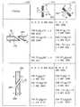
도 1A는 전기 전도체와 같은 복수의 신축 소자들을 포함하는 디스플레이 패널(10)의 일부에 대한 도면이며, 신축 소자들 중 하나는 결함 위치(40)에 절단 결함을 가지며, 트랜지스터(50)과, 전극(60)과 다른 전기 컴포넌트를 포함한다. 디스플레이 패널(10) 상에 나타난 다른 결함은 외부 입자(70)(가령, 먼지와 같은 것으로 패널(10)의 외부 표면 상이나 포토 레지스트(도시되지 않음)와 같은 코팅 아래에 묻혀 발견될 수 있다)와, 화학 잔여물(75) 그리고 두 개의 전도체들(20) 사이의 바람직하지 않은 전기 연결을 형성하는 쇼트(78)를 포함한다. 예를 들면, 결함 위치에서의 결함 유형(예, 절단, 입자, 쇼트나 다른 결함의 종류)을 분류하기 위하여, 디스플레이 패널(10)은 결함 위치(40)에서의 검사를 필요로 한다. 후보 결함 위치의 존재는 초기 자동화된 검사에 의해(예를 들면, 이 경우에 필요치 않는 경우 에도, 이스라엘, 야브네에 위치한 오르보텍 사의 SuperVisionTM이나 InVisionTM을 사용하여) 결정될 수 있다.FIG. 1A is a diagram of a portion of a
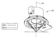
본 발명의 실시예에 따르면, 방향성 특정 조명을 제공하며, 광축(90)의 중앙에 위치한 불스 아이(80, bull's-eye)에 의해 개략적으로 나타내진 다색, 다방향 검사 장치가 본 발명의 실시예에 따라 제 1 조명 모드에서 동작한다. 도시된 바와 같이, 제 1 조명 모드는 광축으로부터 이동되며, 평행하지 않은 축들(일반적으로 직각으로 도시됨)을 따라 공급되는 방향 특정 조명을 포함한다. 평행하지 않은 축들은 검사되는 패널(10) 상의 전도체(20)에 실질적으로 평행하다. 제 1 조명 모드가 예를 들면, 두 개의 상반된 방향으로부터 직진한 파랑("B"로 나타냄)과 같은 제 1 파장길이의 조명과, 제 1 두 개의 상반된 방향에 대하여 평행하지 않은 두 개의 추가로 상반된 방향으로부터 나온 빨강("R"로 나타냄)과 같은 제 2 파장길이의 조명을 포함한다. 축(90)을 따라 보면, 조명된 위치에서 제 1 파장길이의 조명에 대한 응답이 제 2 파장길이의 조명과 구별된다.According to an embodiment of the present invention, a multicolor, multidirectional inspection apparatus, which is schematically represented by a bull's-
도 1B는 도 1A에 도시된 디스플레이 패널을 나타내는 도면으로, 여기서 디스플레이 패널은 제 2 조명 모드에서 동작하는 도 1A의 다색, 다방향 조사 장치를 사용하여 검사된다. 도 1B의 제 2 조명 모드에서, 또한 조명은 광축으로부터 이동되며, 평행하지 않은 축들(일반적으로 직교하는 것으로 도시됨)을 따라 공급되는 방향 특정 조명을 포함한다. 여기서, 평행하지 않은 축들은 검사중인 패널(10) 상의 전도체에 대하여 바람직하게 기울어진다. 제 2 조명 모드는 예를 들면, 검사 중 인 패널(10)의 평면에서 45도 만큼, 제 1 조명 모드에서 사용되는 한 쌍의 제 1 조명 방향으로부터 떨어진 두 개의 상반된 방향들로부터 직진한 파랑("B"로 나타냄)과 같은 제 1 파장길이의 조명을 포함한다. 또한, 제 2 조명 모드에서 사용되는 상반된 두 개의 제 1 방향들에 수직인 두 개의 상반된 추가 방향으로부터 직진한 빨강("R"로 나타냄)과 같은 제 2 파장의 조명을 포함한다. 빨강과 파랑 조명이 도시되었으나, 패널(10) 상의 위치를 조망할 때, 상호 구별가능한 응답을 가지는 적합한 다른 형태의 조명이 사용될 수 있다는 것이 주의한다. 이러한 다른 형태의 조명은 예를 들면, 다른 스펙트라 내의 조명, 편광에 의해 구별되는 조명, 서로 다른 펄스 주파수에서 제공되는 펄스화된 조명 또는 다른 적합한 특성에 의해 구별가능한 조명을 포함한다.FIG. 1B is a view of the display panel shown in FIG. 1A, wherein the display panel is inspected using the multicolor, multidirectional illumination device of FIG. 1A operating in a second illumination mode. In the second illumination mode of FIG. 1B, the illumination also includes a direction specific illumination that is moved from the optical axis and supplied along non-parallel axes (generally shown to be orthogonal). Here, the non-parallel axes are preferably inclined with respect to the conductor on the
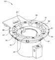
도 2는 도 1A 및 도 1B에 각각 도시된 두 개의 선택가능한 조명 모드에서 조명을 제공하기 위한 본 발명의 실시예에 따라 구성되고 동작하는 조명 슬리브(100)를 나타낸다. 조명 슬리브(100, sleeve)는 선택적으로 동작 가능한 발광 다이오드(R1-R8, B1-B4)와 같은 복수의 조명기를 포함한다. 발광 다이오드는 도 1A 및1B의 제 1 및 제 2 조명 모드들을 제공한다. 바람직하게 다이오드는 복수의 방향들(가령, 0, 45, 90, 135, 180, 225, 270 및 315도의 8 방위각 원점들) 각각에서 하나 이상의 다이오드 세트를 포함한다. 선택적으로, 에지와 같은 기대 방향 특성에 의해 결정되는 기대 방향 각각을 조명할 수 있는 하나 이상의 각을 포함하는 다른 그룹의 각들이 사용될 수 있다. 다음의 LED와 같은 어떤 적합한 LED도 사용될 수 있다. 즉 아길런트 테크놀러지의 상용 LED(파랑: Cat.No. HLMP CB-18UVA00; 빨 강:Cat.No.HLMP EG08-Y2000)를 사용할 수 있다.FIG. 2 shows a
일반적으로, 파랑과 같은 하나의 색을 가지는 조명기 세트가 제 1 조명 경로를 정의하도록 서로 상반되게 배치되며, 반면에 빨강과 같은 제 2 색을 가지는 조명기 세트는 제 1 조명 경로에 평행하지 않은 제 2 조명 경로를 정의하도록 서로 상반되게 배치된다. 빨강 다이오드의 각 세트는 일반적으로 두 개의 다이오드를 포함하며, 반면에 파랑 다이오드의 각 세트는 일반적으로 하나의 다이오드를 포함한다. 왜냐하면, 실시예에서, 두 개의 빨강 다이오드가 충분한 밝기를 획득하는데 필요하기 때문이다. 다이오드 기술의 향상의 위해 그리고 조명 명도에 대한 애플리케이션 필요성을 위해, 각 색에 대해 동일한 다이오드 개수를 가지는 것이 적합하다. 상술한 실시예에서, 한 쌍 빨강 다이오드들(R1 및 R2; R3 및 R4; R5 및 R6; 그리고 R7 및 R8)이 0, 45, 180 및 250도 각 위치 각각에서 개별적으로 중앙에 위치한다. 반면에, 하나의 파랑 다이오드(B1, B2, B3, 및 B4)가 90, 135, 270, 및 315도 각각에 개별적으로 위치한다.In general, a set of fixtures with one color, such as blue, are disposed opposite each other to define a first lighting path, while a set of fixtures with a second color, such as red, are not parallel to the first light path. They are arranged opposite each other to define the lighting path. Each set of red diodes typically contains two diodes, while each set of blue diodes typically contains one diode. This is because in the embodiment, two red diodes are needed to obtain sufficient brightness. For the improvement of diode technology and the need for application for lighting brightness, it is suitable to have the same number of diodes for each color. In the above embodiment, the pair of red diodes R1 and R2; R3 and R4; R5 and R6; and R7 and R8 are individually centered at each of 0, 45, 180 and 250 degrees respectively. On the other hand, one blue diode (B1, B2, B3, and B4) is individually located at 90, 135, 270, and 315 degrees, respectively.
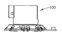
도 3A-3C는 도 2에 도시된 조명기 슬리브(100)의 측면, 끝단 그리고 바닥 형상을 각각 나타낸다. 본 발명의 일 실시예에 따라, 비디오의 대상 렌즈 상부로 미끄러지도록 조명기 슬리브(100)의 크기가 결정되어 다색 방향 특정 조명이 이하에 상술되는 바와 같이 제공된다.3A-3C show the side, end and bottom shapes of the
도 4A는 제 1 조명 모드에서 동작하는 도 2-3C에 도시된 조명기 슬리브(100)를 나타내는 광선 도면이다. 도 4B는 제 2 조명 모드에서 동작하는 도 2-3C에 도시된 조명기를 나타내는 광선 도면이다. 두꺼운 화살표가 빨강과 같은 제 1 색의 광 선을 나타내는 반면, 두껍지 않은(얇은) 화살표가 파랑과 같은 제 2 색의 광선을 나타낸다. 그리고 점선이 광축(90)을 나타낸다.4A is a light ray diagram illustrating the
본 발명의 일 실시예에서, 조명이 공급되는 수직 각도(θ)가 선택되어, 후보 결함의 위치를 보여주는 카메라에 의해 이미지화될 때 입자 및 절단 결함의 개별적인 밝기를 최적화한다. 어두운 영역 조명 각들(θ, α)가 도 4C에 도시된다. 각 (θ)가 수직 축(z)(패널의 x-y 평면에 수직인 축)으로부터 표시된 조명 광선에 대해 측정된다. 각도(α)는 조명 광선의 검사될 패널의 x-y 평면에 위치한 회전각이나 방위각 원점에 대응하는 각도이다.In one embodiment of the invention, the vertical angle θ at which illumination is supplied is selected to optimize the individual brightness of the particle and cutting defects when imaged by a camera showing the location of the candidate defects. Dark area illumination angles θ, α are shown in FIG. 4C. The angle [theta] is measured for the illumination light rays indicated from the vertical axis z (axis perpendicular to the x-y plane of the panel). The angle α is the angle corresponding to the rotation angle or azimuth origin located in the x-y plane of the panel to be inspected of the illumination beam.
전형적으로, 제조 중인 평판 디스플레이에서, 전도체와 같은 신축 소자는 구분가능한 에지를 가지며 행 및 열 내에 배열되어 매트릭스를 정의한다. 절단, 스크래치 및 쇼트(short)와 같은 다른 구조 및 결함 또한 구분가능한 에지를 가진다. 수직 각도(θ)가, 입자와 같은 다른 검출가능한 구조에 대한 에지 노출을 피하도록 그리고 가능한 에지와 입자들 사이의 노출 균일성을 최적화하도록 선택된다. 조명의 제 1 및 제 2 축들 각각이 전도체 방향 중 하나에 각도(α)에 수직이 되도록 선택될 수 있다. 본 발명의 일 실시예에서, 지정된 위치에 있는 전도체의 위치 상태가 알려지지 않거나 이미지 프레임 내에서 변경될 수 있다. 따라서, 도 1A 및 1B에대하여 상술한 제 1 및 제 2 조명 모드가 제공된다.Typically, in flat panel displays under manufacture, stretchable elements, such as conductors, have distinguishable edges and are arranged in rows and columns to define a matrix. Other structures and defects such as cuts, scratches and shorts also have distinguishable edges. The vertical angle θ is chosen to avoid edge exposure to other detectable structures, such as particles, and to optimize exposure uniformity between possible edges and particles. Each of the first and second axes of illumination may be selected to be perpendicular to the angle α in one of the conductor directions. In one embodiment of the invention, the positional state of the conductor at the designated position may be unknown or may change within the image frame. Thus, the first and second illumination modes described above with respect to FIGS. 1A and 1B are provided.
도 4D는 수직 각도(θ)를 선택하는 데 도움이 되는 유용한 그래프이다. 도 4D는 조명의 수직 각도(기울기, θ)의 함수로써, 패널 상의 조명된 전도체 에지의 명도에 대한 선택 조명된 입자의 명도 비율을 선택된 입자에 대해 표시한다. 따라 서 각각의 선택된 입자에 대해, 조명에 대한 응답 명도가 측정되고 에지에 대해 조명에 대한 응답 명도로 나누어진다. 응답 명도는 일반적으로 일정하다. 이후에, 결과가 표준화되고, 표준화된 결과가 표시된다. 곡선(110)은 조명된 에지에 관하여 조명된 입자의 명도를 나타내는 지정된 수직 각도(θ)에서 각 입자에 대한 결과들의 평균값을 연결한다.4D is a useful graph to help select the vertical angle θ. 4D shows, for the selected particles, the brightness ratio of the selected illuminated particles to the brightness of the illuminated conductor edges on the panel as a function of the vertical angle of the illumination (tilt, θ). Thus, for each selected particle, the response brightness for illumination is measured and divided by the response brightness for illumination for the edge. The response brightness is generally constant. Thereafter, the results are standardized and the standardized results are displayed. Curve 110 links the average value of the results for each particle at a specified vertical angle θ that represents the brightness of the illuminated particle with respect to the illuminated edge.
도 4D의 그래프에 나타낸 바와 같이, 수직 각도(θ)가 65도에 근접함에 따라, 평균 표준화된, 에지의 조명에 대한 응답 명도에 대해 입자의 조명에 대한 명도 비율이 1에 근접하며, 이는 입자 및 에지에 대한 상대 명도의 평균이 거의 동일하다는 것을 의미한다. 도 4D에 나타냈지만, 입자와 에지 사이의 조명 명도의 균일성 때문에, 65도에 가까운 수직 각도(θ)가 바람직하다. 본 발명의 실시예에서, 물리적 제한(예를 들면 대상 렌즈의 작동 거리에 대한 제한)에 기인하여, 수직 각도(θ)가 약 60가 되도록 선택된다.As shown in the graph of FIG. 4D, as the vertical angle θ approaches 65 degrees, the ratio of brightness to illumination of the particle approaches 1 for the average normalized, response brightness to illumination of the edge, which is the particle. And mean relative brightness to edge is approximately equal. Although shown in FIG. 4D, a vertical angle θ close to 65 degrees is preferred because of the uniformity of illumination brightness between particles and edges. In an embodiment of the present invention, due to physical limitations (e.g., a limitation on the working distance of the target lens), the vertical angle θ is selected to be about 60.
구체적으로, 도 4A 및 4B에 도시된 바와 같은 두 개의 제한 조명 모드들의 제공이 제한 요소가 되도록 한 것은 아니다. 선택적으로, 둘 이상 또는 둘 이하의 조명 모드를 이용하여 절단과 같은 방향성 국부 효과를 외부 입자와 같은 비 방향성 국부 효과와 구별할 수 있다. 또한, 두 가지 색의 조명을 제공하는 것이 제한적인 것이 아니다. 선택적으로, 하나의 색이나 다색 조명이 사용될 수 있으며, 이 경우에 추가 이미지들이 획득되며, 예를 들면, 이미지들 각각은 시간 도메인(domain)에서 구별가능하다. 또한, 도 4E 및 4F에 예로써 도시된 바와 같이 둘 이상의 색이 사용되거나, 편광 또는 펄스 주파수와 같은 일부 다른 특징들에 의해 구별 가능한 조명에 의해 직접 조명되는 이미지들이 사용될 수 있다. 도 4E 및 4F의 이미지들 모두가 획득되고 비교되거나, 또는 이러한 삼색 이미지 중 하나만이 획득될 수 있다.Specifically, the provision of two limited illumination modes as shown in FIGS. 4A and 4B is not intended to be a limiting element. Optionally, more than one or less than two illumination modes can be used to distinguish directional local effects, such as truncation, from non-directional local effects such as external particles. In addition, providing two colors of illumination is not limiting. Alternatively, one color or multicolor illumination may be used, in which case additional images are obtained, for example each of the images is distinguishable in the time domain. Further, more than one color may be used as shown by way of example in FIGS. 4E and 4F, or images directly illuminated by illumination distinguishable by some other feature, such as polarization or pulse frequency. Both images of FIGS. 4E and 4F may be acquired and compared, or only one of these three color images may be obtained.
구체적으로, 도 4A 및 4B의 실시예에서, 두 그룹의 조명기들({파랑:0도, 180도; 빨강: 90도, 270도} 및 {파랑:135도, 315도; 빨강:45도, 225도})이 존재하며, 선택적으로 조명기들이 다른 배치가 이용될 수 있다. 예를 들어, 각 조명 모드에서, 각 색에 대해 두 개의 다른 조명 방향들(도 4A-4B의 실시예에서 180도 분리됨)을 사용하는 대신에 각 색에 대해 단일 조명 방향을 사용할 수 있다. 따라서, 방향 특정 조명의 배치가 검사될 패널 상 위치한 서로 다른 각도의 전도체에 적용된다.Specifically, in the embodiment of FIGS. 4A and 4B, two groups of illuminators ({blue: 0 degrees, 180 degrees; red: 90 degrees, 270 degrees}) and {blue: 135 degrees, 315 degrees; red: 45 degrees, 225 degrees), optionally other arrangements of fixtures may be used. For example, in each illumination mode, a single illumination direction may be used for each color instead of using two different illumination directions (180 degrees separated in the embodiments of FIGS. 4A-4B) for each color. Thus, the arrangement of directional specific illumination is applied to conductors of different angles located on the panel to be inspected.
도 4G의 실시예에서, 전도체(또는 다른 신축 소자, 이 명세서에서 "전도체"라는 용어는 일 예로써 사용됨)의 조명이 일반적으로 상반된 방향으로부터의 동종의 것이 아니다. 더욱이, 조명의 회전 각도에 대해 일반적으로 수직이라고 가정하면, 조명원에 인접한 전도체 에지가 조명원으로부터 떨어진 전도체 에지보다 더 밝게 보일 수 있다. 전도체가 조명에 의해, 에지에 거의 수직이 아닌 각도(α)로부터 빛을 받는 경우에, 전도체가 어둡게 보일 수 있으며 보이지 않거나 검출되지 않을 수 있다. 이미지 분석 관점으로부터, 바람직하게 형성된 알려진 방향으로 확장하는 에지들의 보이지 않는 것이 바람직하며, 절단, 스크래치, 회로를 쇼트시킬 수 있는 금속성 형성물과 같은 전도체의 형성 중의 결함 및 외부 소자와 같은 다양한 변형물이 이미지에서 강조되도록 한다.In the embodiment of FIG. 4G, the illumination of the conductor (or other stretchable element, where the term “conductor” is used as an example), is generally not the same from the opposite direction. Moreover, assuming that it is generally perpendicular to the angle of rotation of the illumination, the conductor edges adjacent to the illumination source may appear brighter than the conductor edges away from the illumination source. When the conductor receives light from an angle α that is almost perpendicular to the edge, the conductor may appear dark and may not be visible or detected. From the point of view of image analysis, it is desirable to be invisible of the edges extending in the known direction, preferably formed, and various modifications such as defects during the formation of conductors such as metallic formations that can short circuit, scratch, short circuit and external elements such as Make sure it is highlighted in the image.
도 4G는 구분가능한 조명의 방향 특성 성질을 나타낸다. 예를 들어, 도 4G의 전도체(120)에 대해, 조명의 제 1 모드에서 에지(III 및 IV)가 빨강 및 파랑 조명 모두에 응답하여 어둡게 나타난다. 이는 전도체가 위치한 기판에 대해 직각인 광축을 따라 획득된 이미지에 나타난다.4G shows the directional characteristic properties of distinguishable illumination. For example, for
도 4G에 도시된 조명의 제 2 모드에서, 전도체가 놓인 기판에 대해 직각인 광축을 따라 획득된 이미지에, 전도체(125)의 에지(III 및 IV)가 도시된 바와 같이 빨강에 응답하여 나타난다. 그러나, 에지(III)가 에지(IV)보다 다소 강하게(즉, 좀더 깊이 있게) 보인다. 거꾸로, 에지(III, IV) 모두가 도시된 바와 같이 파랑 조명에 응답하여 어둡게 보이며 어느 것도 보이지 않을 수동 있다. 이와 같이, 조명의 방향을 변경하여, 패터닝된 기판 내의 다양한 공지의 구조물(예, 전도체 에지)가 원하는 데로, 획득 이미지에서 선택적으로 가시화되거나 감추어질 수 있다.In the second mode of illumination shown in FIG. 4G, in the image obtained along the optical axis perpendicular to the substrate on which the conductor is placed, the edges III and IV of the
도시된 실시예에서, 각각 두 개의 이웃한 광원들 사이의 각이 90도(각 조명 모드에서)이다. 이러한 구조는 전도체 라인이 일반적으로 균일한 열과 행 내에 배열된 FPD 패널의 분석에 적합하다. 상기 열과 행에는 전도체 라인이 0도, ±45도, 90도 및 135도의 각에서 두드러지게 발생한다. 그러나, 본 발명의 선택 실시예에 따르면, 광원들 사이의 각이 지정된 조사 애플리케이션의 필요에 따라 변경될 수 있다.In the embodiment shown, the angle between each two neighboring light sources is 90 degrees (in each illumination mode). This structure is suitable for analysis of FPD panels in which conductor lines are generally arranged in uniform columns and rows. In the columns and rows, conductor lines are prominent at angles of 0 degrees, ± 45 degrees, 90 degrees and 135 degrees. However, according to an optional embodiment of the present invention, the angle between the light sources can be changed as needed for the designated irradiation application.
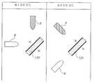
도 5A 및 5B는 도 1A 및 1B 각각의 제 1 및 제 2 조명 모드 하에서 절단 결함-신축 소자 구조의 여러 유형의 외관을 나타내는 표이다. 도 5A의 표의 좌측 열(200)은 수평으로 배치된 전기 전도체("전도체"라는 용어는 여기에 단지 신축 소자의 예시로 사용됨)로 이루어진 부분(210)과, 수직으로 배치된 전기 전도체의 부 분(220)과, 수직으로 배치된 절단 결함(240)이 존재하는 세로로 배치된 전기 전도체의 부분(230)과, 수직으로 배치된 절단 결함(260)이 존재하는 세로로 배치된 전기 전도체의 부분(250)과 그리고 수직으로 배치된 절단 결함(280)이 존재하는 비스듬히 배치된 전기 전도체의 부분(270)과 같은 복수의 미세 구조들을 나타낸다.5A and 5B are tables showing the appearance of various types of cut defect-stretch device structures under the first and second illumination modes of FIGS. 1A and 1B, respectively. The
도 5B의 표에 도시된 좌측 열(200)은 비스듬히 배치된 절단 결함(294)이 존재하는 수평으로 배치된 전기 전도체의 부분(292)과, 비스듬히 배치된 절단 결함(298)이 존재하는 세로로 배치된 전기 전도체의 부분(296)과 같은 복수의 미세 구조를 도시한다.The
도 5A 및 5B에 도시된 표의 중간 열(310)은 개략적으로 도시된 제 1 조명 모드(320) 하에서, 열(200) 내의 다양한 구조의 외관을 나타낸다. 제 1 조명 모드에서 파랑 조명이 수평 축을 따라 양방향으로부터 제공되며, 빨강 조명이 수직 축을 따라 양방향으로부터 제공된다. 도 5A-5B의 표에 도시된 우측 열(330)은, 개략적으로 도시된 제 2 어두운 영역 조명 모드(340) 하에서, 열(200) 내의 다양한 구조의 외관을 나타낸다. 제 2 조명 모드(340)에서, 파랑 조명이 135-316도 축을 따라 양방향으로부터 제공되며, 빨강 조명이 45-225 도 축을 따라 양방향으로부터 제공된다. 도시된 바와 같이, 두꺼운 선으로 표시된 다른 신축 소자 전도체 에지나 점선으로 표시된 절단 에지와 같은 에지들(지정 색의 조명 방향과 직각을 이룸)이 이러한 색으로 나타난다. 두꺼운 선으로 표시된 신축 소자 에지들이나 점선으로 표시된 절단 에지와 같은 에지들(예를 들면 45도 각에서, 조명의 방향에 대해 각을 이룸)이 어둡게 보인다. 색이 특징적으로 열(310, 330)에 표시된 구조 부분 이외의 구조 들은 어둡게 나타난다.The
도 6은 도 1A 및 1B 각각에 도시된 제 1 및 제 2 조명 모드 하의 외부 입자-전기 전도체 구조의 여러 유형의 외관들을, 열(310, 330)에 나타내는 표이다. 도 6의 첫 번째 형상은 먼지와 같은 외부 입자(420)를 포함하는 수평 전도체(400)이다. 도 6의 두 번째 형상은 먼지 입자(440)이 놓여 있는 수직 전도체(430)이다. 도 6의 세번 째 형상은 먼지 입자(460)이 놓여 있는 비스듬한 전도체(450)이다. 외부 입자들(420, 440, 460)이 패널의 표면상에 전체적으로 존재하여 포토 레지스트 코딩과 같은 코팅 하부에서 관찰되거나 포함된다. 도시된 바와 같이, 먼지 입자상 불규칙한 에지가 과다하게 존재 함에 의해, 외부 입자는 다양한 방향으로부터 입사된 조명을 산란하고, 서로 다른 색을 가지는 방향 특정 조명에 의해 비춰질 때, 두 개의 조명 모드에서 보라와 같은 혼합 색(방향 특정 색들이 빨강과 파랑인 경우에)으로 보인다. 이는 외부 입자가 도 5A-5B에 도시된 다양한 절단 결함들과 명확히 구별되도록 한다. 절단면들은 일반적으로 특정 방향으로 공급되는 조명에서 보이나, 다른 방향으로 공급되는 조명에서는 보이지 않는다.FIG. 6 is a table showing, in
도 5A, 5B 및 6, 열(310, 330)에 부분(270, 450)의 위치와 절단 결함(292, 298)의 위치에 대해 지정된 각도 범위의 최종점은 특정 애플리케이션에 대한 예시이며, 모든 애플리케이션에 대해 적합한 것은 아니다. 열(310, 330)의 세 개의 부분들에 대한 정보가 작은 각, 중간 각 및 큰 각에 대해 일반적으로 정확하나, 작은 각, 중간 각 및 큰 각 범위의 정확한 컷-오프 포인트는 도시된 바와 같이 15 도 및 75 도일 필요가 없다. 그리고 바람직하게는, 각 애플리케이션에 대해 경험적으로 결정된다.5A, 5B and 6, end points in the angular range specified for the location of
도 5A, 5B 및 6에 도시된 표는, 먼지나 선택적으로는 다양한 방향성을 가지는 절단 결함에 기인하여, 조명 모드들(330, 340) 각각의 이용하여 획득된 결함이나 후보 결함의 이미지 쌍의 검사에 의해, 인-라인이나 오프-라인 자동 검사 시스템에서 오퍼레이터나 결함 또는 후보 결함을 분류하는 적합한 이미지 처리 시스템에 사용될 수 있다.The tables shown in FIGS. 5A, 5B, and 6 show inspection of image pairs of defects or candidate defects obtained using each of the
다음의 결함 분류 스킴(scheme)은, 도 1A 및 1B의 실시예에 따라 빨강 및 파랑 방향성 특정 조명을 포함하는 장치 내 결함의 유형을 분류하는 데 사용된다. 예를 들면 다름과 같다.The following defect classification scheme is used to classify the types of defects in a device that include red and blue directional specific illumination in accordance with the embodiment of FIGS. 1A and 1B. For example:
전도체 에지가 제 1 조명 모드에서 빨강이고 제 2 조명 모드에서 어둡게 나타나며, 결함이 제 1 조명 모드에서 파랑이고 제 2 조명 모드에서 어둡게 나타나는 경우에, 결함은 수평 방향 전도체의 절단 결함이다.If the conductor edge is red in the first illumination mode and appears dark in the second illumination mode, and the defect is blue in the first illumination mode and dark in the second illumination mode, the defect is a cutting defect in the horizontal conductor.
전도체 에지가 제 1 조명 모드에서 빨강이고 제 2 조명 모드에서 어둡게 나타나며, 결함이 제 1 조명 모드에서 어둡게 나타나고 제 2 조명 모드에서 파랑인 경우에, 결함은 수평 방향 전도체의 절단 결함이다.If the conductor edges are red in the first illumination mode and dark in the second illumination mode, and the defects are dark in the first illumination mode and blue in the second illumination mode, the defect is a cutting defect in the horizontal conductor.
전도체 에지가 제 1 조명 모드에서 빨강이고 제 2 조명 모드에서 어둡게 나타나며, 결함이 제 1 조명 모드에서 빨강이고 제 2 조명 모드에서 어둡게 나타나는 경우에, 결함은 수평 방향 전도체의 절단 결함이다.If the conductor edges are red in the first illumination mode and dark in the second illumination mode, and the defects are red in the first illumination mode and dark in the second illumination mode, the defect is a cutting defect in the horizontal conductor.
전도체 에지가 제 1 조명 모드에서 파랑이고 제 2 조명 모드에서 어둡게 나타나며, 결함이 제 1 조명 모드에서 빨강이고 제 2 조명 모드에서 어둡게 나타나는 경우에, 결함은 수직 방향 전도체의 절단 결함이다.If the conductor edge is blue in the first illumination mode and appears dark in the second illumination mode, and the defect is red in the first illumination mode and dark in the second illumination mode, the defect is a cutting defect in the vertical conductor.
전도체 에지가 제 1 조명 모드에서 파랑이고 제 2 조명 모드에서 어둡게 나타나며, 결함이 제 1 조명 모드에서 어둡게 나타나고 제 2 조명 모드에서 빨강인 경우에, 결함은 절단 결함(형체(298), 양의 기울기)이다.If the conductor edge is blue in the first illumination mode and dark in the second illumination mode, and the defect is dark in the first illumination mode and red in the second illumination mode, the defect is a cutting defect (
전도체 에지가 제 1 조명 모드에서 파랑이고 제 2 조명 모드에서 어둡게 나타나며, 결함이 제 1 조명 모드에서 어둡게 나타나고 제 2 조명 모드에서 파랑인 경우에, 결함은 절단 결함(형체(298), 음의 기울기)이다.If the conductor edge is blue in the first illumination mode and dark in the second illumination mode, and the defect is dark in the first illumination mode and blue in the second illumination mode, the defect is a cutting defect (
전도체 에지가 제 1 조명 모드에서 파랑이고 제 2 조명 모드에서 어둡게 나타나며, 결함이 제 1 조명 모드에서 파랑이고 제 2 조명 모드에서 어둡게 나타나는 경우에, 결함은 절단 결함이다.If the conductor edge is blue in the first illumination mode and appears dark in the second illumination mode, and the defect is blue in the first illumination mode and dark in the second illumination mode, the defect is a cutting defect.
유사하게, 전도체 에지가 제 1 조명 모드에서 어둡게 나타나고 제 2 조명 모드에서 빨강인 경우에, 결함이 전방으로 기운 전도체를 따라 관찰되며, 도 5 및 6의 테이블에서 결함 부분의 분석에 따라 분류가 적합하게 고안될 수 있다.Similarly, when the conductor edges appear dark in the first illumination mode and red in the second illumination mode, defects are observed along the forward tilted conductors and the classification is appropriate according to the analysis of the defect portions in the tables of FIGS. 5 and 6. It can be designed to be.
제 1 조명 모드 및 제 2 조명 모드 모두에서 결함이 혼합색인 경우(균일하지 않게 배열된 빨강 및 파랑 조명 컴포넌트들을 포함함), 전도체 에지들의 색과 방향에 상관없이, 전형적으로 결함은 광 확산 입자이다.If the defect is a mixed color (including non-uniformly arranged red and blue lighting components) in both the first and second illumination modes, typically the defect is a light diffusing particle, regardless of the color and orientation of the conductor edges. .
서로 다른 색들을 사용하여, 방향 정보가 단일 이미지에서 사용 가능하도록 한다. 마찬가지로, 방향 특정 조명으로 조명된 시간 분리 이미지의 시퀀스(sequence)에 방향 정보가 사용가능할 수 있다. 그러나, 방향 특정 색 조명을 사용하여, 동일한 위치의 서로 다른 시간 분리 이미지에 나타나는 결함들 사이의 정 보 및 상관 등록에 대한 다양한 어려움이 제거된다. 여기서는 서로 다른 색들이 참조되는 반면에, 또 다른 구별 가능한 광학 특성을 가지는 조명(예, 편광이나 펄스 주파수)가 사용될 수 있다.Different colors are used to make the orientation information available in a single image. Similarly, direction information may be available to a sequence of time separated images illuminated with direction specific illumination. However, using directional specific color illumination, various difficulties in registering information and correlation between defects appearing in different time-separated images of the same location are eliminated. While different colors are referenced here, illumination with another distinguishable optical characteristic (eg polarization or pulse frequency) may be used.
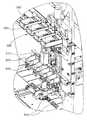
도 7A-7B는 홀더와 덮개가 제거된 도 2의 조명기를 포함하는 본 발명의 실시예에 따라 구성되고 동작하는 스캐닝 자동 광 검사 및 비디오 검증 시스템을 나타내는 조감도이다. 도 8은, 원(500)으로 표시된 도 7A-7B에 도시된 두 개의 광학 헤드 중 하나의 확대도이다. 도 9는 도 8에 잘 도시된 바와 같이 광학 페드의 결함 검증 카메라 시스템(510)을 나타내는 측면도이다. 이하에 구체적으로 기술된 바를 제외하고는, 도 7A-9의 장치는 이스라엘 야브네에 위치한 오보텍 사의 상용 SuperVisionTM 자동 광 검사 시스템과 유사할 수 있다.7A-7B are aerial views illustrating a scanning automatic light inspection and video verification system constructed and operative in accordance with an embodiment of the present invention including the illuminator of FIG. 2 with a holder and a cover removed. 8 is an enlarged view of one of the two optical heads shown in FIGS. 7A-7B, indicated by
도 7A-7B의 스캐닝 및 비디오 검증 시스템은 일반적으로 워크피스(530)가 y 축(550)을 따라 이동하도록 장착된 공기 부유 테이블(520)과 같은 동작-테이블을 포함한다. 도 7A-7B의 자동 광학 검사 및 비디오 검증 시스템에 사용하기에 적합한 부상 컨베이어(levitating conveyer)가 미국 특허 제6,810,297호에 더욱 자세히 기술되며, 이의 명세서가 전체적으로 여기에 참조 문헌으로 포함된다. 도 7B에서, 워크피스(530)가 제거되어 있다. 광학 브리지(560)가 하나 이상의 광학 헤드(570)(도시된 실시예에서는 두 개의 광학 헤드. 하나는 광학 브리지(560)에 의해 직접 서포트되고, 다른 하나는 서브-브리지(574)에 의해 서포트 됨). 각 광학 헤드(570)는 x 축(540)을 따라 동작하도록 장착되며 카메라 서브유닛의 어레이(580)를 포함한다 (네 개의 각 서브유닛이 실시예로 도시됨). 각 카메라 서브 유닛은 스캔 카메라(590)와 같은 카메라와, 스캔 카메라 광학 장치(600) 및 스캔 조명기(610)를 포함한다. 하나 이상의 광학 헤드(570)는 또한 하나 이상의 결함 검증 카메라 서브유닛(510)(이러한 서브 유닛 하나가 실시예로 도시됨)이 도 9를 참조하여 상술한 바와 같이 포함된다.The scanning and video verification system of FIGS. 7A-7B generally includes an action-table, such as an air floatation table 520, mounted such that the
도 9에 상세히 나타낸 결함 검증 카메라 서브시스템(510)은 일반적으로 고 해상도 비디오 현미경으로 구성되며, 비디오 카메라(예, 덴마크의 JAI 사의 상용 CCD 카메라)와 같은 카메라(700)와, 고 배율 광학장치를 제공하는 튜브 렌즈(710)와 도 2-4B의 다방향 다중 분광 슬리브(100)와 같은 암 영역 조명(720)을 포함한다. 여기서 슬리브(100)는 Lecia 10x/0.3 대물렌즈와 같은 대물 렌즈(725)에 적합하다. 바람직하게는, 다중색 조명원(732)으로부터 광섬유 광학장치(735)를 거쳐 다중색 광을 받아들이는 명 영역 조명기(730)가 제공되며, 비디오 카메라가 광축(790)을 따라 워크피스를 보이는 동안에, 빔 스플리터(740)가 광축(790)을 따라 워크피스(도시되지 않음)를 향해 명 영역 조명기로부터의 조명을 향한다. 명 영역 조명기(730)나 암 영역 조명기(720) 또는 두 조명의 조합 어느 것으로부터도 조명이 제공될 수 있다.The defect
도 10은 본 발명의 바람직한 실시예에 따라 구성되며 동작하는 자동 광 검사 시스템을 나타내는 개략적인 기능 블록도이다. 자동 광 검사 시스템은 방향 조명 정보를 사용하여 워크피스 결함들을 분류하기 위하여 현미경 구조를 가지는 워크피스 내에 위치한 후보 결함 위치를 직접 조명하기 위한 것이다. 도 10의 자동 광 검 사 시스템은 자동 광 검사 시스템(가령, 이스라엘 야브네에 위치한 오보텍 사의 상용 SuperVisionTM시스템과 같은워크피스 스캐닝 자동 광 검사 서브 시스템(1000)을 포함한다. 워크피스 스캐닝 서브시스템은 또한 특정 워크피스 위치들(L1, L2, L3, ...)에 위치한 후보 결함들을 나타내기 위해 동작하는 이미지 처리 기능성을 가진다. 다색 방향 특정 비디오 검증 서브시스템(1010)은 워크피스 스캐닝 서브시스템(100)으로부터 후보 결함 위치들을 입력받으며, 암 영역 조명을 사용하여, 전형적으로는 방향 특정 색 조명을 제공하는 도 2-4B 및 9와 같은 다색 다중 방향 광학 헤드를 사용하여, 이러한 위치들을 이미지화함으로써 후보 결함 위치들을 검증한다. 서브 시스템(1000, 1010)은 SuperVisionTM시스템에서와 같이 집적되어 형성되며, 다라서 두 개의 서브 시스템의 거의 대부분의 구성요소들과 특히 동작 테이블 및 이들의 관련 동작 제공기가 예를 들면, 도 7A-7B에 도시된 바와 같이 공유된다.10 is a schematic functional block diagram illustrating an automated light inspection system constructed and operative in accordance with a preferred embodiment of the present invention. The automated light inspection system is for direct illumination of candidate defect locations located within a microscopeed workpiece to classify workpiece defects using directional illumination information. The automated light inspection system of FIG. 10 is an automated light inspection system (e.g., commercially available SuperVision™ from Obovotech, located in Yavne, Israel). Such as system Workpiece Scanning Automated
비디오 검증 서브시스템에 의해 조명이 후보 결함 위치를 조명하는 방향에 대해 색이 코딩되고 광축으로부터 오프셋 된 조명을 사용하여, 방향성 있게 조명된 후보 결함들의 이미지들이 상술한 바와 같이 생성된다. 이러한 이미지들은 도 5A, 5B 및 6의 표에 도시된 바와 유사할 수 있다. 방향성 있게 조명된 후보 결함 이미지들이 방향 정보 처리 서브 시스템(1020)(예, 이스라엘 야브네에 위치한 오보텍 사의 상용 SuperVisionTM자동 광 검사 시스템이 공급된 비디오 이미지 처리 패키지)로 입력된다. 본 발명의 일 실시예에서, 비디오 이미지 처리 패키지는 결함 분 류 습득 패키지를 포함하며, 결함 종류를 정의하는 결함 유형의 데이터 베이스(1050)를 참조하여 이미지를 분석한다. 각각의 새로운 후보 결함이 가장 밀접하게 일치되는 결함 유형으로 분류된다. 또는 이외의 다른 적합한 기준에 의해 선택적으로 특정 후보 결함들이 외부 입자들과 같은 비 결함으로 간주할 있다. 후보 결함의 분류가 결함 데이터 베이스(1060) 내의 컴퓨터 메모리에 저장된다.Images of directionally illuminated candidate defects are generated, as described above, using illumination coded with respect to the direction in which the illumination illuminates the candidate defect location by the video verification subsystem and offset from the optical axis. Such images may be similar to those shown in the tables of FIGS. 5A, 5B and 6. Directionally illuminated candidate defect images are displayed on the orientation information processing subsystem 1020 (e.g., commercially available SuperVisionTM from Obovotech, located in Yavne, Israel). The automatic light inspection system is fed into a supplied video image processing package. In one embodiment of the invention, the video image processing package includes a defect classification acquisition package, and analyzes the image with reference to a database of
도 11은 도 10에 도시된 방향 정보 처리 서브시스템과 결함 종류 정의 데이터 베이스(1050)를 설정하도록 하기 위하여, 셋 업 서브시스템(1030)에 의해 수행되는 방법을 나타내는 개략적인 흐름도이다. 단계(1100)에서, 셋 업 서브 시스템은, 광축으로부터 오프셋 된 방향 특정 조명하에서 비디오 이미지 장치(가령, 비디오 결함 검증 서브 시스템(1010))에 의해, 수집된 기본 결함들을 수집하고 분석한다. 단계(1110)에서, 각 기본 또는 표본 결함이 결함 유형(예, 수평 절단 결함, 수직 절단 결함 또는 먼지)으로 지정된다. 상술한 결함 유형 분류는 고도로 간략화되는 것이 적합하며, 실제로는 매우 많은 수의 결함 분류 유형과 하위 유형이 존재할 수 있다. 단계(1120)에서, 충분한 표본들이 축적되어 각각의 바람직한 결함 종류를 정의한다. 그렇지 않으면, 단계(1120)가 통과될 때까지, 단계(1100, 1110)가 반복된다. 단계(1130)에서, 결함 유형의 특성을 정의하는 동작이 습득되고, 도 10에 도시된 결함 종류 정의 데이터 베이스(1050) 내에 저장된다. 결함 분류 프로세스의 정확도가 계산되고(단계(1140)), 단계(1150)에서는 결함 분류를 정의에 대해 바람직한 정확도에 다다랐는지 여부가 확인된다. 그렇지 않은 경우에, 방법은 단계(1100)로 복귀한다.FIG. 11 is a schematic flowchart illustrating a method performed by the
일단 바람직한 정확도에 도달한 하면, 방법은 셋 업이 완료되고 서브 시스템(1020)이, 습득된 결함이나 데이터 베이스(1050)에 저장된 카테고리를 사용하여 후보 결함을 분류를 시작할 준비가 되었다는 신호를 한다. 일반적으로, 결함 분류가 개선되도록 그리고 전도체의 형성중에 나타나는 실제 결함을 외부 입자와 같이 실제 결함이 아닌 후보 결함과 구별하도록 결함 분류 정의를 개선하는 것이 바람직하다. 새로이 분류된 결함들이 결함 데이터 베이스에 추가되어 결함 분류 프로세스가 개선되도록 한다.Once the desired accuracy is reached, the method signals that setup is complete and the
도 12는 도 10에 도시된 서브 시스템의 동작 방법을 나타내는 방향 정보를 설정하는 바람직한 방법을 나타내는 개략적인 흐름도이다. 단계(1200)에서, 워크피스 스캐닝 서브 시스템(1000)은 워크피스를 스캔하고 후보 결함 위치들을 나타낸다. 단계(1210)에서, 제 1 방향 특정 조명하에, 하나 이상의 고 해상도 비디오 이미지가 획득된다. 그리고 단계(1220)에서 하나 이상의 고 해상도 비디오 이미지가, 제 1 방향 특정 조명 하에 획득된다. 선택적으로, 전도체의 주 방향이 지정 위치에 있는 경우에, 제 1 방향 특정 조명하에서 하나의 고 해상도 비디오 이미지만을 획득하기에 적합하다. 제 1 및 제 2 방향 특정 조명은 단일색(monochromatic)이거나 다중색(polychromatic)일 수 있으며, 또는 도 5A-6을 참조하여 예시로써 설명한 바와 같이, 방향 특정 조명이 동일한 이미지에서 둘 이상의 구별가능한 형태의 조명을 포함한다.FIG. 12 is a schematic flowchart illustrating a preferred method of setting direction information indicating a method of operating the subsystem illustrated in FIG. 10. In
단계(1230)에서, 예를 들어, 적합한 전도체 에지들은 어둡게 도시되고 도시되지 않으나, 결함들은 가시화되는 광학 이미지가 선택된다. 단계(1240)에서, 서브 시스템(1010)에 의해 발생한 하나 이상의 비디오 이미지가 제공되어 서브 시스템(1020)의 결함 분류기로 제공된다. 단계(1250)에서, 셋 업 동안에 서브 시스템(1030)에 의해 사전 지정되고 결함 종류 정의 데이터 베이스(1050)에 저장된 결함 분류를 사용하여, 서브 시스템(1020)이 후보 결함들을 비결함(예, 표면상에 위치하거나 표면 코딩 하부에 위치한 외부 입자들)이거나 하나의 분류나 다른 분류의 결함들인지에 따라 분류한다.In
본 발명에 따른 일 실시예의 장점 중 하나는, 순서 없는 에지들의 복잡성에 기인하여, 입자가 모든 방향으로부터 입사된 빛을 산란하고 따라서 방향 특정 빛의 복합 응답이 일어남으로써, 결함 식별이 쉬워 진다는 것이다. 반대로, 절단 결함이나 쇼트와 같이, 전도체 형성시 발생하는 결함들은 일반적으로 주 방향을 가지므로, 방향 특정 조명이 비칠 때, 주 응답을 나타낸다. 방향 특정 빛이 색 코드화(color coded)될 때, 입자들은 다색 응답을 나타내는 반면에, 절단, 스크래치, 쇼트 등과 같은 전도체 내의 결함인 형성 결함은 주(predominant)색 응답을 나타낸다. 추가로, 본 발명의 일 실시예에 따르면, 조명의 방향에 관하여 색 코드화된 방향 특정 조명이 최소 시간에 최소 개수의 이미지들을 포착하거나 획득할 수 있도록 한다. 바람직하게는, 후보 결함 영상화를 위해 사용되는, 빨강 및 파랑과 같은 색들이 색 비디오 카메라에 의해 완전히 구분 가능하게 된다(노이즈 레벨 내).One of the advantages of one embodiment according to the invention is that due to the complexity of the unordered edges, the particles scatter the light incident from all directions and thus the complex response of the direction specific light makes defect identification easier. . Conversely, defects that occur during conductor formation, such as cut defects or shorts, generally have a main direction and thus exhibit a main response when directional specific illumination is illuminated. When directional specific light is color coded, particles exhibit a multicolor response, whereas formation defects, which are defects in conductors such as cuts, scratches, shorts and the like, exhibit a predominant color response. In addition, according to one embodiment of the present invention, color-coded direction specific illumination with respect to the direction of illumination enables to capture or acquire the minimum number of images in minimum time. Preferably, colors such as red and blue, which are used for candidate defect imaging, are fully distinguishable by the color video camera (within noise level).
본 발명의 소프트웨어 구성요소들이 필요한 경우에, ROM(read only memory) 형식으로 구현가능하다. 소프트웨어 구성요소들은 필요한 경우에, 일반적인 기술을 사용하여 하드웨어 내에 구현될 수 있다.If software components of the present invention are needed, they may be implemented in a read only memory (ROM) format. Software components may be implemented in hardware using general techniques, if desired.
상술한 본 발명의 실시예들은 단지 예시와 설명을 위한 것일 뿐이며, 본 발명을 설명된 형태로 한정하려는 것이 아니다. 따라서, 다양한 변화 및 변경을 할 수 있음은 본 발명이 속하는 분야의 당업자에게 자명하다. 또한, 이 명세서의 상세한 설명이 본 발명의 범위를 제한하는 것은 아니다. 본 발명의 범위는 첨부된 청구항에 의해서 정의된다.The above-described embodiments of the present invention are for illustration and description only, and are not intended to limit the present invention to the described form. Accordingly, various changes and modifications can be made to those skilled in the art to which the present invention pertains. In addition, the detailed description of this specification does not limit the scope of the present invention. The scope of the invention is defined by the appended claims.
이와 같이 본 발명에 따르면, 디스플레이 패널과 같은 제조 대상물 상에 결함을 검사함에 있어, 절단이나 스크래치 등과 같은 형성 결함과 외부 입자를 구별함으로써, 향상된 검사 시스템 및 방법을 제공할 수 있다.As described above, according to the present invention, in inspecting defects on a manufacturing object such as a display panel, it is possible to provide an improved inspection system and method by distinguishing external particles from forming defects such as cutting or scratching.
또한, 본 발명에 따르면, 조명의 방향에 관하여 색 코드화된 방향 특정 조명이 최소 시간에 최소 개수의 이미지들을 포착하거나 획득할 수 있도록 한다.In addition, according to the present invention, color-coded direction specific illumination with respect to the direction of illumination enables to capture or acquire the minimum number of images in minimum time.
Claims (30)
Translated fromKoreanApplications Claiming Priority (2)
| Application Number | Priority Date | Filing Date | Title |
|---|---|---|---|
| US11/339,835US7391510B2 (en) | 2006-01-26 | 2006-01-26 | System and method for inspecting patterned devices having microscopic conductors |
| US11/339,835 | 2006-01-26 |
Publications (2)
| Publication Number | Publication Date |
|---|---|
| KR20070078372Atrue KR20070078372A (en) | 2007-07-31 |
| KR101401146B1 KR101401146B1 (en) | 2014-05-29 |
Family
ID=38285180
Family Applications (1)
| Application Number | Title | Priority Date | Filing Date |
|---|---|---|---|
| KR1020070004118AExpired - Fee RelatedKR101401146B1 (en) | 2006-01-26 | 2007-01-15 | System And Method For Inspecting Patterned Devices Having Microscopic Conductors |
Country Status (6)
| Country | Link |
|---|---|
| US (1) | US7391510B2 (en) |
| JP (1) | JP5520434B2 (en) |
| KR (1) | KR101401146B1 (en) |
| CN (1) | CN101008622B (en) |
| IL (1) | IL179995A0 (en) |
| TW (1) | TWI428584B (en) |
Families Citing this family (15)
| Publication number | Priority date | Publication date | Assignee | Title |
|---|---|---|---|---|
| US7636466B2 (en)* | 2006-01-11 | 2009-12-22 | Orbotech Ltd | System and method for inspecting workpieces having microscopic features |
| JP4882505B2 (en)* | 2006-05-19 | 2012-02-22 | 東京エレクトロン株式会社 | Method and apparatus for collating foreign matter distribution pattern |
| DE202007019013U1 (en)* | 2007-11-01 | 2010-04-29 | Zimmermann & Schilp Handhabungstechnik Gmbh | Devices for inspection and irradiation of sheet materials |
| JP4503643B2 (en)* | 2007-12-06 | 2010-07-14 | 本田技研工業株式会社 | Metal belt inspection device |
| DE102008057131B4 (en) | 2007-12-06 | 2013-05-29 | Honda Motor Co., Ltd. | Riemenprüfvorrichtung |
| JP4611404B2 (en)* | 2008-06-04 | 2011-01-12 | 本田技研工業株式会社 | Belt inspection device |
| KR100913181B1 (en)* | 2008-01-14 | 2009-08-20 | 삼성모바일디스플레이주식회사 | Input device of inspection equipment for flat panel display |
| JP5622338B2 (en)* | 2008-12-12 | 2014-11-12 | アズビル株式会社 | Method for discriminating and checking foreign matter and scratch marks in semiconductor device manufacturing process |
| US9035673B2 (en)* | 2010-01-25 | 2015-05-19 | Palo Alto Research Center Incorporated | Method of in-process intralayer yield detection, interlayer shunt detection and correction |
| CN102830123B (en)* | 2012-08-16 | 2014-07-02 | 北京科技大学 | On-line detection method of small defect on metal plate strip surface |
| JP5655045B2 (en)* | 2012-09-11 | 2015-01-14 | 株式会社日立ハイテクノロジーズ | Optical surface defect inspection apparatus and optical surface defect inspection method |
| JP2014145656A (en)* | 2013-01-29 | 2014-08-14 | Nikka Kk | Method and device for visualizing fine particle adhesion state |
| CN104392432A (en)* | 2014-11-03 | 2015-03-04 | 深圳市华星光电技术有限公司 | Histogram of oriented gradient-based display panel defect detection method |
| US20170118384A1 (en)* | 2015-10-26 | 2017-04-27 | National Applied Research Laboratories | Adaptive lighting device for optical inspection |
| US11580398B2 (en)* | 2016-10-14 | 2023-02-14 | KLA-Tenor Corp. | Diagnostic systems and methods for deep learning models configured for semiconductor applications |
Family Cites Families (34)
| Publication number | Priority date | Publication date | Assignee | Title |
|---|---|---|---|---|
| JP2914967B2 (en)* | 1986-08-27 | 1999-07-05 | 株式会社日立製作所 | Appearance inspection method |
| JP2524532B2 (en)* | 1989-10-11 | 1996-08-14 | 日立電子エンジニアリング株式会社 | Wafer particle inspection system |
| JPH06201747A (en)* | 1992-12-25 | 1994-07-22 | Sharp Corp | Pattern flaw inspecting device |
| JPH06229937A (en)* | 1993-02-05 | 1994-08-19 | Nec Yamagata Ltd | Inspection apparatus for circuit pattern of semiconductor device |
| JPH085575A (en)* | 1994-06-21 | 1996-01-12 | Hitachi Electron Eng Co Ltd | Method and apparatus for detecting foreign matter protrusion of color filter |
| JPH09196859A (en)* | 1996-01-23 | 1997-07-31 | Nec Corp | Surface defect inspection device |
| JPH09257642A (en)* | 1996-03-18 | 1997-10-03 | Hitachi Electron Eng Co Ltd | Glass substrate defect type determination method |
| US6092059A (en)* | 1996-12-27 | 2000-07-18 | Cognex Corporation | Automatic classifier for real time inspection and classification |
| US6118524A (en)* | 1997-02-26 | 2000-09-12 | Acuity Imaging, Llc | Arc illumination apparatus and method |
| JP3460541B2 (en)* | 1997-10-20 | 2003-10-27 | 日産自動車株式会社 | Method and apparatus for inspecting defects on inspected surface |
| US6256093B1 (en)* | 1998-06-25 | 2001-07-03 | Applied Materials, Inc. | On-the-fly automatic defect classification for substrates using signal attributes |
| US6366690B1 (en) | 1998-07-07 | 2002-04-02 | Applied Materials, Inc. | Pixel based machine for patterned wafers |
| JP3566589B2 (en)* | 1998-07-28 | 2004-09-15 | 株式会社日立製作所 | Defect inspection apparatus and method |
| IL126866A (en)* | 1998-11-02 | 2003-02-12 | Orbotech Ltd | Apparatus and method for fabricating flat workpieces |
| US6922482B1 (en)* | 1999-06-15 | 2005-07-26 | Applied Materials, Inc. | Hybrid invariant adaptive automatic defect classification |
| US7061601B2 (en)* | 1999-07-02 | 2006-06-13 | Kla-Tencor Technologies Corporation | System and method for double sided optical inspection of thin film disks or wafers |
| JP3688520B2 (en) | 1999-07-06 | 2005-08-31 | 住友化学株式会社 | Surface inspection apparatus and surface inspection method |
| US6763130B1 (en)* | 1999-07-21 | 2004-07-13 | Applied Materials, Inc. | Real time defect source identification |
| DE10041354A1 (en)* | 1999-08-24 | 2001-04-12 | Hitachi Electr Eng | Foreign particle or defect checking system for inspection of substrate or wafer, has size information processing device which processes size of foreign particle or defect on predetermined object |
| JP2001168160A (en)* | 1999-12-07 | 2001-06-22 | Sony Corp | System for inspecting semiconductor wafer |
| US6465801B1 (en)* | 2000-07-31 | 2002-10-15 | Hewlett-Packard Company | Dust and scratch detection for an image scanner |
| US6731384B2 (en)* | 2000-10-10 | 2004-05-04 | Hitachi, Ltd. | Apparatus for detecting foreign particle and defect and the same method |
| JP4230674B2 (en)* | 2001-03-01 | 2009-02-25 | 株式会社日立製作所 | Defect inspection apparatus and method |
| JP2002303586A (en)* | 2001-04-03 | 2002-10-18 | Hitachi Ltd | Defect inspection method and defect inspection device |
| JP4038356B2 (en)* | 2001-04-10 | 2008-01-23 | 株式会社日立製作所 | Defect data analysis method and apparatus, and review system |
| TWI222423B (en) | 2001-12-27 | 2004-10-21 | Orbotech Ltd | System and methods for conveying and transporting levitated articles |
| JP3551188B2 (en) | 2002-01-10 | 2004-08-04 | オムロン株式会社 | Surface condition inspection method and substrate inspection device |
| JP2003271927A (en)* | 2002-03-18 | 2003-09-26 | Hitachi High-Technologies Corp | Defect inspection method |
| DE10323139A1 (en)* | 2003-05-22 | 2004-12-23 | Leica Microsystems Jena Gmbh | Method and device for high-resolution fault finding and classification |
| JP2005037281A (en) | 2003-07-16 | 2005-02-10 | Nec Plasma Display Corp | Manufacturing method of display device, inspection method of substrate for display device, and inspection device of substrate for display device |
| JP2005156957A (en) | 2003-11-26 | 2005-06-16 | Nec Saitama Ltd | Display inspecting device of liquid crystal display and its display inspecting method |
| JPWO2005119227A1 (en)* | 2004-06-04 | 2008-04-03 | 株式会社東京精密 | Semiconductor appearance inspection device and lighting method |
| DE102004029014B4 (en)* | 2004-06-16 | 2006-06-22 | Leica Microsystems Semiconductor Gmbh | Method and system for inspecting a wafer |
| WO2006006148A2 (en)* | 2004-07-12 | 2006-01-19 | Negevtech Ltd. | Multi mode inspection method and apparatus |
- 2006
- 2006-01-26USUS11/339,835patent/US7391510B2/enactiveActive
- 2006-12-11ILIL179995Apatent/IL179995A0/enunknown
- 2006-12-13TWTW095146732Apatent/TWI428584B/enactive
- 2007
- 2007-01-15KRKR1020070004118Apatent/KR101401146B1/ennot_activeExpired - Fee Related
- 2007-01-23CNCN200710003640.8Apatent/CN101008622B/ennot_activeExpired - Fee Related
- 2007-01-25JPJP2007014808Apatent/JP5520434B2/ennot_activeExpired - Fee Related
Also Published As
| Publication number | Publication date |
|---|---|
| CN101008622A (en) | 2007-08-01 |
| JP5520434B2 (en) | 2014-06-11 |
| KR101401146B1 (en) | 2014-05-29 |
| JP2007199066A (en) | 2007-08-09 |
| IL179995A0 (en) | 2007-10-31 |
| US20070171404A1 (en) | 2007-07-26 |
| CN101008622B (en) | 2015-05-20 |
| TW200728709A (en) | 2007-08-01 |
| TWI428584B (en) | 2014-03-01 |
| US7391510B2 (en) | 2008-06-24 |
Similar Documents
| Publication | Publication Date | Title |
|---|---|---|
| KR101401146B1 (en) | System And Method For Inspecting Patterned Devices Having Microscopic Conductors | |
| CN101783306B (en) | Systems and methods for inspecting wafers | |
| EP2387796B1 (en) | System and method for inspecting a wafer | |
| EP2387794B1 (en) | System and method for inspecting a wafer | |
| TWI558996B (en) | System and method for capturing illumination reflected in multiple directions | |
| CN101726499B (en) | Surface inspection apparatus | |
| JP2003503701A (en) | Lighting module | |
| KR101650138B1 (en) | Multiple surface inspection system and method | |
| CN111458294B (en) | Inspection device | |
| US7220034B2 (en) | Fiber optic darkfield ring light | |
| WO2022174013A1 (en) | System and methods for enhanced illumination lighting for optical inspection to detect object defects | |
| KR102764860B1 (en) | Mini LED bonding Bonding Posture Measurement Device using a shadow Image | |
| JP2004264276A (en) | Surface inspection device and surface inspection method | |
| HK40006797B (en) | System and method for inspecting a wafer | |
| HK40006797A (en) | System and method for inspecting a wafer | |
| WO2001036929A2 (en) | Via inspection with an optical inspection system | |
| JP2002139440A (en) | Illuminator for pattern inspection | |
| HK1165905A (en) | System and method for capturing illumination reflected in multiple directions |
Legal Events
| Date | Code | Title | Description |
|---|---|---|---|
| PA0109 | Patent application | St.27 status event code:A-0-1-A10-A12-nap-PA0109 | |
| PG1501 | Laying open of application | St.27 status event code:A-1-1-Q10-Q12-nap-PG1501 | |
| A201 | Request for examination | ||
| PA0201 | Request for examination | St.27 status event code:A-1-2-D10-D11-exm-PA0201 | |
| R17-X000 | Change to representative recorded | St.27 status event code:A-3-3-R10-R17-oth-X000 | |
| D13-X000 | Search requested | St.27 status event code:A-1-2-D10-D13-srh-X000 | |
| D14-X000 | Search report completed | St.27 status event code:A-1-2-D10-D14-srh-X000 | |
| R17-X000 | Change to representative recorded | St.27 status event code:A-3-3-R10-R17-oth-X000 | |
| E902 | Notification of reason for refusal | ||
| PE0902 | Notice of grounds for rejection | St.27 status event code:A-1-2-D10-D21-exm-PE0902 | |
| R17-X000 | Change to representative recorded | St.27 status event code:A-3-3-R10-R17-oth-X000 | |
| T11-X000 | Administrative time limit extension requested | St.27 status event code:U-3-3-T10-T11-oth-X000 | |
| T11-X000 | Administrative time limit extension requested | St.27 status event code:U-3-3-T10-T11-oth-X000 | |
| P11-X000 | Amendment of application requested | St.27 status event code:A-2-2-P10-P11-nap-X000 | |
| P13-X000 | Application amended | St.27 status event code:A-2-2-P10-P13-nap-X000 | |
| E701 | Decision to grant or registration of patent right | ||
| PE0701 | Decision of registration | St.27 status event code:A-1-2-D10-D22-exm-PE0701 | |
| GRNT | Written decision to grant | ||
| PR0701 | Registration of establishment | St.27 status event code:A-2-4-F10-F11-exm-PR0701 | |
| PR1002 | Payment of registration fee | St.27 status event code:A-2-2-U10-U11-oth-PR1002 Fee payment year number:1 | |
| PG1601 | Publication of registration | St.27 status event code:A-4-4-Q10-Q13-nap-PG1601 | |
| R18-X000 | Changes to party contact information recorded | St.27 status event code:A-5-5-R10-R18-oth-X000 | |
| FPAY | Annual fee payment | Payment date:20170420 Year of fee payment:4 | |
| PR1001 | Payment of annual fee | St.27 status event code:A-4-4-U10-U11-oth-PR1001 Fee payment year number:4 | |
| FPAY | Annual fee payment | Payment date:20180417 Year of fee payment:5 | |
| PR1001 | Payment of annual fee | St.27 status event code:A-4-4-U10-U11-oth-PR1001 Fee payment year number:5 | |
| R18-X000 | Changes to party contact information recorded | St.27 status event code:A-5-5-R10-R18-oth-X000 | |
| FPAY | Annual fee payment | Payment date:20190417 Year of fee payment:6 | |
| PR1001 | Payment of annual fee | St.27 status event code:A-4-4-U10-U11-oth-PR1001 Fee payment year number:6 | |
| PR1001 | Payment of annual fee | St.27 status event code:A-4-4-U10-U11-oth-PR1001 Fee payment year number:7 | |
| PR1001 | Payment of annual fee | St.27 status event code:A-4-4-U10-U11-oth-PR1001 Fee payment year number:8 | |
| PR1001 | Payment of annual fee | St.27 status event code:A-4-4-U10-U11-oth-PR1001 Fee payment year number:9 | |
| PR1001 | Payment of annual fee | St.27 status event code:A-4-4-U10-U11-oth-PR1001 Fee payment year number:10 | |
| PC1903 | Unpaid annual fee | St.27 status event code:A-4-4-U10-U13-oth-PC1903 Not in force date:20240523 Payment event data comment text:Termination Category : DEFAULT_OF_REGISTRATION_FEE | |
| PC1903 | Unpaid annual fee | St.27 status event code:N-4-6-H10-H13-oth-PC1903 Ip right cessation event data comment text:Termination Category : DEFAULT_OF_REGISTRATION_FEE Not in force date:20240523 |