KR20070076488A - Touch panels, touch input position detection methods, electro-optical devices, and electronic devices - Google Patents
Touch panels, touch input position detection methods, electro-optical devices, and electronic devicesDownload PDFInfo
- Publication number
- KR20070076488A KR20070076488AKR1020070004373AKR20070004373AKR20070076488AKR 20070076488 AKR20070076488 AKR 20070076488AKR 1020070004373 AKR1020070004373 AKR 1020070004373AKR 20070004373 AKR20070004373 AKR 20070004373AKR 20070076488 AKR20070076488 AKR 20070076488A
- Authority
- KR
- South Korea
- Prior art keywords
- touch panel
- surface acoustic
- cover film
- acoustic wave
- touch
- Prior art date
- Legal status (The legal status is an assumption and is not a legal conclusion. Google has not performed a legal analysis and makes no representation as to the accuracy of the status listed.)
- Granted
Links
Images


Classifications
- G—PHYSICS
- G06—COMPUTING OR CALCULATING; COUNTING
- G06F—ELECTRIC DIGITAL DATA PROCESSING
- G06F3/00—Input arrangements for transferring data to be processed into a form capable of being handled by the computer; Output arrangements for transferring data from processing unit to output unit, e.g. interface arrangements
- G06F3/01—Input arrangements or combined input and output arrangements for interaction between user and computer
- G06F3/03—Arrangements for converting the position or the displacement of a member into a coded form
- G06F3/041—Digitisers, e.g. for touch screens or touch pads, characterised by the transducing means
- G06F3/043—Digitisers, e.g. for touch screens or touch pads, characterised by the transducing means using propagating acoustic waves
- G06F3/0436—Digitisers, e.g. for touch screens or touch pads, characterised by the transducing means using propagating acoustic waves in which generating transducers and detecting transducers are attached to a single acoustic waves transmission substrate
- G—PHYSICS
- G02—OPTICS
- G02F—OPTICAL DEVICES OR ARRANGEMENTS FOR THE CONTROL OF LIGHT BY MODIFICATION OF THE OPTICAL PROPERTIES OF THE MEDIA OF THE ELEMENTS INVOLVED THEREIN; NON-LINEAR OPTICS; FREQUENCY-CHANGING OF LIGHT; OPTICAL LOGIC ELEMENTS; OPTICAL ANALOGUE/DIGITAL CONVERTERS
- G02F1/00—Devices or arrangements for the control of the intensity, colour, phase, polarisation or direction of light arriving from an independent light source, e.g. switching, gating or modulating; Non-linear optics
- G02F1/01—Devices or arrangements for the control of the intensity, colour, phase, polarisation or direction of light arriving from an independent light source, e.g. switching, gating or modulating; Non-linear optics for the control of the intensity, phase, polarisation or colour
- G02F1/13—Devices or arrangements for the control of the intensity, colour, phase, polarisation or direction of light arriving from an independent light source, e.g. switching, gating or modulating; Non-linear optics for the control of the intensity, phase, polarisation or colour based on liquid crystals, e.g. single liquid crystal display cells
- G02F1/133—Constructional arrangements; Operation of liquid crystal cells; Circuit arrangements
- G02F1/1333—Constructional arrangements; Manufacturing methods
- G02F1/13338—Input devices, e.g. touch panels
- G—PHYSICS
- G06—COMPUTING OR CALCULATING; COUNTING
- G06F—ELECTRIC DIGITAL DATA PROCESSING
- G06F1/00—Details not covered by groups G06F3/00 - G06F13/00 and G06F21/00
- G06F1/16—Constructional details or arrangements
- G06F1/1613—Constructional details or arrangements for portable computers
- G06F1/1633—Constructional details or arrangements of portable computers not specific to the type of enclosures covered by groups G06F1/1615 - G06F1/1626
- G06F1/1637—Details related to the display arrangement, including those related to the mounting of the display in the housing
- G06F1/1643—Details related to the display arrangement, including those related to the mounting of the display in the housing the display being associated to a digitizer, e.g. laptops that can be used as penpads
- G—PHYSICS
- G06—COMPUTING OR CALCULATING; COUNTING
- G06F—ELECTRIC DIGITAL DATA PROCESSING
- G06F3/00—Input arrangements for transferring data to be processed into a form capable of being handled by the computer; Output arrangements for transferring data from processing unit to output unit, e.g. interface arrangements
- G06F3/01—Input arrangements or combined input and output arrangements for interaction between user and computer
- G06F3/03—Arrangements for converting the position or the displacement of a member into a coded form
- G06F3/033—Pointing devices displaced or positioned by the user, e.g. mice, trackballs, pens or joysticks; Accessories therefor
- G06F3/0354—Pointing devices displaced or positioned by the user, e.g. mice, trackballs, pens or joysticks; Accessories therefor with detection of 2D relative movements between the device, or an operating part thereof, and a plane or surface, e.g. 2D mice, trackballs, pens or pucks
- G06F3/03547—Touch pads, in which fingers can move on a surface
- G—PHYSICS
- G06—COMPUTING OR CALCULATING; COUNTING
- G06F—ELECTRIC DIGITAL DATA PROCESSING
- G06F3/00—Input arrangements for transferring data to be processed into a form capable of being handled by the computer; Output arrangements for transferring data from processing unit to output unit, e.g. interface arrangements
- G06F3/01—Input arrangements or combined input and output arrangements for interaction between user and computer
- G06F3/03—Arrangements for converting the position or the displacement of a member into a coded form
- G06F3/041—Digitisers, e.g. for touch screens or touch pads, characterised by the transducing means
- G06F3/0412—Digitisers structurally integrated in a display
- G—PHYSICS
- G06—COMPUTING OR CALCULATING; COUNTING
- G06F—ELECTRIC DIGITAL DATA PROCESSING
- G06F3/00—Input arrangements for transferring data to be processed into a form capable of being handled by the computer; Output arrangements for transferring data from processing unit to output unit, e.g. interface arrangements
- G06F3/01—Input arrangements or combined input and output arrangements for interaction between user and computer
- G06F3/03—Arrangements for converting the position or the displacement of a member into a coded form
- G06F3/041—Digitisers, e.g. for touch screens or touch pads, characterised by the transducing means
- G06F3/0416—Control or interface arrangements specially adapted for digitisers
- G06F3/04166—Details of scanning methods, e.g. sampling time, grouping of sub areas or time sharing with display driving
Landscapes
- Engineering & Computer Science (AREA)
- Theoretical Computer Science (AREA)
- General Engineering & Computer Science (AREA)
- Physics & Mathematics (AREA)
- General Physics & Mathematics (AREA)
- Human Computer Interaction (AREA)
- Acoustics & Sound (AREA)
- Computer Hardware Design (AREA)
- Nonlinear Science (AREA)
- Crystallography & Structural Chemistry (AREA)
- Optics & Photonics (AREA)
- Chemical & Material Sciences (AREA)
- Mathematical Physics (AREA)
- Position Input By Displaying (AREA)
Abstract
Translated fromKoreanDescription
Translated fromKorean도 1은 실시예 1에 따른 전기 광학 장치의 단면도,1 is a sectional view of an electro-optical device according to
도 2는 액정 장치의 분해 사시도,2 is an exploded perspective view of a liquid crystal device;
도 3은 터치 패널 기판의 평면도,3 is a plan view of a touch panel substrate,
도 4(a) 및 도 4(b)는 터치 입력 위치에서의 표면 탄성파의 감쇠 작용의 설명도,4 (a) and 4 (b) are explanatory views of the attenuation action of the surface acoustic wave at the touch input position;
도 5는 제어부의 블럭도,5 is a block diagram of a control unit;
도 6(a) 및 도 6(b)는 스페이서 위치에서의 표면 탄성파의 감쇠 작용의 설명도,6 (a) and 6 (b) are explanatory views of the attenuation action of the surface acoustic wave at the spacer position;
도 7(a)∼도 7(c)는 스페이서 위치의 근방을 누른 경우에 있어서의 표면 탄성파의 감쇠 작용의 설명도,7 (a) to 7 (c) are explanatory diagrams of the attenuation action of the surface acoustic wave when the vicinity of the spacer position is pressed;
도 8(a)∼도 8(c)는 스페이서 위치를 누른 경우에 있어서의 표면 탄성파의 감쇠 작용의 설명도,8 (a) to 8 (c) are explanatory views of the attenuation action of surface acoustic waves when the spacer position is pressed;
도 9는 실시예 2에 따른 전기 광학 장치의 설명도,9 is an explanatory diagram of an electro-optical device according to a second embodiment;
도 10은 실시예 3에 따른 전기 광학 장치의 설명도,10 is an explanatory diagram of an electro-optical device according to a third embodiment;
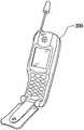
도 11은 휴대전화의 사시도.11 is a perspective view of a mobile phone.
본 발명은 터치 패널, 터치 입력 위치 검출 방법, 전기 광학 장치, 및 전자기기에 관한 것이다.The present invention relates to a touch panel, a touch input position detection method, an electro-optical device, and an electronic device.
최근, 휴대정보단말기(PDA), 팜탑(palm-top) 컴퓨터 등의 소형 정보 전자기기의 보급에 따라, 액정 표시 패널 상에 입력 장치로서 터치 패널을 탑재한 액정 장치가 널리 사용되도록 되고 있다.In recent years, with the spread of small information electronic devices such as PDAs and palm-top computers, liquid crystal devices having touch panels as input devices on liquid crystal display panels have been widely used.
그 중, 초음파 표면 탄성파 방식의 터치 패널에 있어서는, 유리 기판의 표면 상을 전파하는 표면 탄성파가 터치 입력 위치에서 감쇠하는 성질을 이용하여, 터치 입력 위치가 검출된다.Among them, in the touch panel of the ultrasonic surface acoustic wave method, the touch input position is detected using the property that the surface acoustic wave propagating on the surface of the glass substrate is attenuated at the touch input position.
이 터치 패널의 일례로서, 일본 특허 공개 2004-348686호 공보에 개시되어 있는 바와 같이, 표면 탄성파가 전파하는 유리 기판과, 표면 탄성파를 송수신하는 트랜스듀서와, 트랜스듀서가 수신한 표면 탄성파에 근거하여 터치 위치를 검출하는 위치 검출부와, 유리 기판에 대하여 공간층을 사이에 두고 배치되고, 유리 기판의 기판 대향면에 복수의 도트 스페이서가 형성된 투명 수지 필름을 구비한 터치 패널이 제안되어 있다.As an example of this touch panel, as disclosed in Japanese Patent Laid-Open No. 2004-348686, a glass substrate through which surface acoustic waves propagate, a transducer for transmitting and receiving surface acoustic waves, and a surface acoustic wave received by the transducer There is proposed a touch panel provided with a position detection unit for detecting a touch position and a transparent resin film disposed with a space layer interposed therebetween with a plurality of dot spacers formed on a substrate facing surface of the glass substrate.
이 투명 수지 필름은, 물체가 접촉하지 않을 때는 기판 대향면이 유리 기판 에 접촉하지 않고, 물체가 접촉했을 때는 기판 대향면이 유리 기판에 접촉하도록 구성되어 있다.This transparent resin film is comprised so that a board | substrate opposing surface may not contact a glass substrate when an object does not contact, and when a object contacts, a substrate opposing surface will contact a glass substrate.
그리고, 투명 수지 필름이 유리 기판에 접촉한 위치에서의 표면 탄성파의 감쇠를 검지함으로써, 터치 입력 위치를 검출하도록 되어 있다.And a touch input position is detected by detecting the attenuation of the surface acoustic wave in the position which the transparent resin film contacted the glass substrate.
그러나, 유리 기판의 표면을 전파하는 표면 탄성파는 스페이서와의 접촉에 의해서도 감쇠한다.However, surface acoustic waves propagating through the surface of the glass substrate are also attenuated by contact with the spacer.
상기한 특허문헌의 터치 패널에서는, 터치 입력이 없는 경우에도, 투명 수지 필름의 휨 등에 의해, 스페이서와 유리 기판이 접촉할 우려가 있다.In the touch panel of the said patent document, even if there is no touch input, there exists a possibility that a spacer and a glass substrate may contact by curvature of a transparent resin film, etc.
또한, 스페이서 위치의 근방이 터치 입력 위치로 된 경우에는, 투명 수지 필름보다 먼저 스페이서가 유리 기판과 접촉할 우려가 있다.Moreover, when the vicinity of a spacer position turns into a touch input position, there exists a possibility that a spacer may contact a glass substrate before a transparent resin film.
이들 경우에는, 스페이서 위치를 터치 입력 위치로서 오(誤) 검출한다는 문제가 있다.In these cases, there is a problem of false detection of the spacer position as the touch input position.
본 발명은, 상기 과제를 해결하기 위해서 이루어진 것으로서, 터치 입력 위치의 오 검출을 방지하는 것이 가능한 터치 패널, 및 그 터치 입력 위치 검출 방법의 제공을 목적으로 한다.This invention is made | formed in order to solve the said subject, and an object of this invention is to provide the touch panel which can prevent the false detection of a touch input position, and its touch input position detection method.
또한, 신뢰성이 우수한 전기 광학 장치 및 전자기기의 제공을 목적으로 한 다.It is also an object of the present invention to provide highly reliable electro-optical devices and electronic devices.
상기 목적을 달성하기 위해, 본 발명에 따른 터치 패널은, 입력면을 구비한 터치 패널 기판과, 상기 터치 패널 기판의 상기 입력면에 대향하여 이간 배치된 커버 필름과, 상기 터치 패널 기판으로부터 상기 커버 필름을 향하여 세워져 마련된 스페이서와, 상기 터치 패널 기판의 상기 입력면에 표면 탄성파를 전파시키는 송신자와, 상기 입력면을 전파한 상기 표면 탄성파를 측정하는 수신자와, 상기 커버 필름을 누르지 않은 상태에서의 상기 표면 탄성파의 측정값을 기준값으로서 저장하는 메모리와, 터치 패널 사용중에 있어서의 상기 표면 탄성파의 측정값과 상기 기준값과의 차분이 유의로 되는 위치를, 터치 입력 위치로서 검출하는 판단부를 포함한다.In order to achieve the above object, a touch panel according to the present invention includes a touch panel substrate having an input surface, a cover film spaced apart from the input surface of the touch panel substrate, and the cover from the touch panel substrate. A spacer provided to face the film, a transmitter for propagating surface acoustic waves to the input surface of the touch panel substrate, a receiver for measuring the surface acoustic waves propagating the input surface, and the cover film in a state of not being pressed And a memory for storing the measured value of the surface acoustic wave as a reference value, and a determination unit for detecting, as a touch input position, a position at which a difference between the measured value of the surface acoustic wave and the reference value during use of the touch panel becomes significant.
이 구성에 의하면, 터치 패널 기판 상에 스페이서가 세워져 마련되어 있기 때문에, 스페이서에 의한 감쇠를 포함하여 표면 탄성파의 기준값을 측정할 수 있다.According to this configuration, since the spacer is placed on the touch panel substrate, the reference value of the surface acoustic wave can be measured including attenuation by the spacer.
이에 따라, 터치 패널 사용중에 있어서의 상기 표면 탄성파의 측정값과 상기 기준값과의 차분은, 스페이서 위치에서 유의로 되지 않는다.Accordingly, the difference between the measured value of the surface acoustic wave and the reference value during use of the touch panel does not become significant at the spacer position.
따라서, 스페이서 위치를 터치 입력 위치로 판단하는 오 검출을 방지할 수 있다.Therefore, it is possible to prevent the false detection of determining the spacer position as the touch input position.
또한, 커버 필름은 가요성(可撓性)을 갖기 때문에, 스페이서 위치의 근방이 터치 입력 위치로 되더라도, 스페이서를 강하게 누르는 일이 없다.Moreover, since a cover film is flexible, even if the vicinity of a spacer position turns into a touch input position, a spacer is not pressed strongly.
그 때문에, 커버 필름을 누르지 않은 상태에서 표면 탄성파의 기준값을 측정 하면 충분한 것으로 되고, 터치 패널의 사용 준비(캘리브레이션) 작업을 간소화할 수 있다.Therefore, it is sufficient if the reference value of the surface acoustic wave is measured while the cover film is not pressed, thereby simplifying the preparation for use (calibration) of the touch panel.
본 발명에 따른 터치 패널의 터치 입력 위치 검출 방법은, 터치 패널 기판의 입력면에 대향하여 이간 배치된 커버 필름을 누르지 않은 상태에서의 표면 탄성파의 측정값을 기준값으로서 기록하는 공정과, 터치 패널 사용중에 있어서의 상기 표면 탄성파의 측정값과 상기 기준값과의 차분이 유의로 되는 위치를 터치 입력 위치로서 검출하는 공정을 포함한다.The touch input position detection method of the touch panel which concerns on this invention is a process of recording the measured value of the surface acoustic wave as a reference value, without pressing the cover film arrange | positioned apart from the input surface of a touch panel board | substrate, and during touch panel use And detecting a position at which a difference between the measured value of the surface acoustic wave and the reference value in the difference becomes significant as a touch input position.
이 방법에 의하면, 스페이서 위치를 터치 입력 위치로 판단하는 오 검출을 방지할 수 있다.According to this method, false detection which judges a spacer position as a touch input position can be prevented.
본 발명에 따른 전기 광학 장치는, 복수의 화소가 정렬 배치된 화상 표시 장치와, 상기 화상 표시 장치의 화상 표시측에 배치된 터치 패널을 포함하고, 상기 터치 패널은, 입력면을 구비한 터치 패널 기판과, 상기 터치 패널 기판의 상기 입력면에 대향하여 이간 배치된 커버 필름과, 상기 터치 패널 기판으로부터 상기 커버 필름을 향하여 세워져 마련된 스페이서와, 상기 터치 패널 기판의 상기 입력면에 표면 탄성파를 전파시키는 송신자와, 상기 입력면을 전파한 상기 표면 탄성파를 측정하는 수신자와, 상기 커버 필름을 누르지 않은 상태에서의 상기 표면 탄성파의 측정값을 기준값으로서 저장하는 메모리와, 터치 패널 사용중에 있어서의 상기 표면 탄성파의 측정값과 상기 기준값과의 차분이 유의로 되는 위치를, 터치 입력 위치로서 검출하는 판단부를 포함한다.An electro-optical device according to the present invention includes an image display device in which a plurality of pixels are arranged and a touch panel arranged on the image display side of the image display device, wherein the touch panel includes a touch panel having an input surface. A substrate, a cover film spaced apart from the input surface of the touch panel substrate, a spacer standing up from the touch panel substrate toward the cover film, and a surface acoustic wave propagating to the input surface of the touch panel substrate. A memory for storing a transmitter, a receiver for measuring the surface acoustic wave propagating through the input surface, a measurement value of the surface acoustic wave in a state in which the cover film is not pressed as a reference value, and the surface acoustic wave in use of the touch panel Determination of detecting a position at which a difference between the measured value of the reference value and the reference value becomes significant as a touch input position. It includes.
이 구성에 의하면, 터치 입력 위치의 오 검출을 방지하는 것이 가능한 터치 패널을 구비하고 있기 때문에, 신뢰성이 우수한 전기 광학 장치를 제공할 수 있다.According to this structure, since the touch panel which can prevent the false detection of a touch input position is provided, the electro-optical device which is excellent in reliability can be provided.
본 발명의 전기 광학 장치에 있어서는, 상기 화상 표시 장치가 상기 터치 패널 기판으로서 기능하는 것이 바람직하다.In the electro-optical device of the present invention, it is preferable that the image display device functions as the touch panel substrate.
이 구성에 의하면, 전기 광학 장치를 박형화할 수 있다.According to this configuration, the electro-optical device can be thinned.
또한, 터치 패널의 스페이서를 화상 표시 장치에 위치를 맞추어 배치할 수 있기 때문에, 화상 표시 장치에서의 복수 화소의 경계 영역에 터치 패널의 스페이서를 정밀하게 배치할 수 있다.Moreover, since the spacer of a touch panel can be arrange | positioned so that it may be located in an image display apparatus, the spacer of a touch panel can be precisely arrange | positioned in the boundary area of the several pixel in an image display apparatus.
본 발명의 전기 광학 장치에 있어서는, 상기 화상 표시 장치는, 액정을 사이에 유지하는 한 쌍의 기판과, 상기 한 쌍의 기판의 외측에 배치된 한 쌍의 편광판을 구비한 액정 장치이며, 상기 한 쌍의 편광판 중 화상 표시측의 상기 편광판이 상기 커버 필름으로서 기능하는 것이 바람직하다.In the electro-optical device of the present invention, the image display device is a liquid crystal device having a pair of substrates holding liquid crystals between them, and a pair of polarizing plates disposed outside the pair of substrates. It is preferable that the said polarizing plate of an image display side among a pair of polarizing plates functions as the said cover film.
이 구성에 의하면, 전기 광학 장치를 박형화할 수 있다.According to this configuration, the electro-optical device can be thinned.
본 발명의 전기 광학 장치에 있어서는, 상기 터치 패널 기판의 연직 방향으로부터 보아, 상기 스페이서는, 상기 화상 표시 장치에서의 상기 복수의 화소의 경계 영역에 배치되어 있는 것이 바람직하다.In the electro-optical device of the present invention, it is preferable that the spacer is disposed at a boundary region of the plurality of pixels in the image display device as viewed from the vertical direction of the touch panel substrate.
이 구성에 의하면, 터치 패널의 스페이서에 기인하는 화상 표시 장치의 개구율의 저하를 억제할 수 있다.According to this structure, the fall of the aperture ratio of the image display apparatus resulting from the spacer of a touch panel can be suppressed.
본 발명에 따른 전자기기는, 상술한 전기 광학 장치를 구비한다.The electronic device which concerns on this invention is equipped with the above-mentioned electro-optical device.
이 구성에 의하면, 터치 입력 위치의 오 검출을 방지하는 것이 가능한 터치 패널을 구비하고 있기 때문에, 신뢰성이 우수한 전자기기를 제공할 수 있다.According to this structure, since the touch panel which can prevent the false detection of a touch input position is provided, the electronic device which is excellent in reliability can be provided.
이하, 본 발명의 실시예에 대하여, 도면을 참조하여 설명한다.EMBODIMENT OF THE INVENTION Hereinafter, embodiment of this invention is described with reference to drawings.
또, 이하의 설명에 이용하는 각 도면에서는, 각 부재를 인식 가능한 크기로 하기 때문에, 각 부재의 축척을 적절히 변경하고 있다.In addition, in each drawing used for the following description, since each member is made into the magnitude | size which can be recognized, the scale of each member is changed suitably.
또, 본 명세서에서는, 액정 장치의 각 구성 부재에서의 액정층측을 내측이라고 부르고, 그 반대측을 외측이라고 부르기로 한다.In addition, in this specification, the liquid crystal layer side in each structural member of a liquid crystal device is called inside, and the opposite side is called outside.
또한, 본 명세서에서는, 터치 패널의 각 구성 부재에서의 터치 입력측을 표면쪽이라고 부르고, 그 반대측을 뒷쪽이라고 부르기로 한다.In addition, in this specification, the touch input side in each structural member of a touch panel is called a surface side, and the opposite side is called a back side.
(실시예 1)(Example 1)
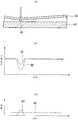
도 1은 실시예 1에 따른 전기 광학 장치의 설명도이며, 도 2의 A-A 선에 상당하는 부분에서의 단면도이다.BRIEF DESCRIPTION OF THE DRAWINGS It is explanatory drawing of the electro-optical device concerning Example 1, and is sectional drawing in the part corresponded to the A-A line of FIG.
도 1에 도시하는 바와 같이, 실시예 1에 따른 전기 광학 장치(100)에 있어서는, 화상 표시 장치인 액정 장치(1)의 화상 표시측(표면쪽)에, 터치 패널(50)이 배치되어 있다.As shown in FIG. 1, in the electro-
(액정 장치)(Liquid crystal device)
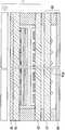
도 2는 액정 장치의 분해 사시도이다.2 is an exploded perspective view of the liquid crystal device.
또, 본 실시예에서는 패시브 매트릭스형의 액정 장치를 예로 하여 설명하지만, 본 발명을 액티브 매트릭스형의 액정 장치에 적용하는 것도 가능하다.In the present embodiment, a passive matrix liquid crystal device is described as an example, but the present invention can also be applied to an active matrix liquid crystal device.
액정 장치(1)에서는, 유리 등의 투명 재료로 이루어지는 한 쌍의 하부 기 판(10) 및 상부 기판(20)이 대향 배치되어 있다.In the
양 기판(10, 20)의 사이에는 스페이서(도시하지 않음)가 배치되고, 양 기판(10, 20)의 간격이 예컨대 5㎛ 정도로 유지되어 있다.Spacers (not shown) are disposed between the two
또한, 양 기판(10, 20)은, 열 경화형이나 자외선 경화형 등의 접착제로 이루어지는 밀봉재(30)에 의해, 주연부가 접합되어 있다.In addition, the peripheral part is joined to both board |
그 밀봉재(30)의 일부에는, 양 기판(10, 20)으로부터 외측으로 돌출한 액정 주입구(32)가 마련되어 있다.A part of the sealing
그 액정 주입구(32)로부터, 양 기판(10, 20)과 밀봉재(30)에 의해 둘러싸인 공간에, STN(Super Twisted Nematic) 액정 등의 액정 재료가 봉입되어 있다.Liquid crystal materials, such as STN (Super Twisted Nematic) liquid crystal, are enclosed from the liquid
그 액정이 주입된 후에, 액정 주입구(32)가 봉지재(封止材)(31)에 의해 봉지되어 있다.After the liquid crystal is injected, the liquid
하부 기판(10)의 내면에는, ITO 등의 투명 도전 재료로 이루어지는 통상 전극(co㎜on electrode)(12)이 스트라이프 형상으로 형성되어 있다.On the inner surface of the
또한, 상부 기판(20)의 내면에는, ITO 등의 투명 도전 재료로 이루어지는 세그먼트 전극(22)이 스트라이프 형상으로 형성되어 있다.Moreover, the
또, 세그먼트 전극(22) 및 통상 전극(12)은 직교하도록 배치되고, 그 교점 부근이 액정 장치의 화소로 되어 있다.Moreover, the
한편, 하부 기판(10)의 외측에는 입사측 편광판(18)이 배치되고, 상부 기판(20)의 외측에는 출사측 편광판(28)이 배치되어 있다.On the other hand, the
또, 입사측 편광판(18) 및 출사측 편광판(28)은, 각각의 투과축이 소정 각 도(예컨대 대략 90°)로 교차하도록 배치되어 있다.Moreover, the incident
또한, 입사측 편광판(18)의 외측에는, 백 라이트(2)가 배치되어 있다.In addition, the
한편, 하부 기판(10)은 상부 기판(20)의 측방에 돌출하여 형성된 돌출부(11)를 갖는다.On the other hand, the
돌출부(11)에는, 통상 전극(12)이 연장되어 형성되어 있다.In the protruding
또한, 돌출부(11)의 선단에는, 액정 장치(1)와 다른 기판을 접속하기 위한 배선 패턴(13)이 형성되어 있다.Moreover, the
그리고, 배선 패턴(13)과 통상 전극(12)과의 사이에는, 다른 기판으로부터의 신호에 근거하여 통상 전극(12)을 구동하기 위한 구동용 IC(38)가 실장되어 있다.A driving
마찬가지로, 상부 기판(20)은 돌출부(21)를 갖는다.Similarly, the
돌출부(21)에는, 세그먼트 전극(22)이 연장되어 형성되고, 세그먼트 전극(22)을 구동하기 위한 구동용 IC(39)가 실장되어 있다.The
도 1에 되돌아가, 하부 기판(10)의 내면에는, 복수의 화소(4)에 대응하여, 컬러 필터를 구성하는 적색(R), 녹색(G) 및 청색(B)의 색재층(16R, 16G, 16B)이 형성되어 있다.Returning to FIG. 1, on the inner surface of the
또, 각 색재층(16R, 16G, 16B)의 사이에는, 차광막(15)이 형성되어 있다.Moreover, the
차광막(15)은 인접하는 화소(4)로부터의 광 누출을 방지한다.The
또한, 각 색재층(16R, 16G, 16B) 및 차광막(15)의 표면에는 평탄화막(보호막)(17)이 형성되어 있다.Further, planarization films (protective films) 17 are formed on the surfaces of the color material layers 16R, 16G, 16B and the
평탄화막(17)의 표면에는, 통상 전극(12)이 형성되어 있다.The
통상 전극(12)의 표면에는, 전계 무인가시의 액정의 배향 상태를 규제하는 배향막(14)이 형성되어 있다.Usually, on the surface of the
한편, 상부 기판(20)의 내면에는 세그먼트 전극(22)이 형성되어 있다.On the other hand, a
세그먼트 전극(22)의 표면에는, 전압 무인가시의 액정의 배향 상태를 규제하는 배향막(24)이 형성되어 있다.On the surface of the
또, 상부 기판(20)의 배향막(24)에 의한 액정의 배향 방향과, 하부 기판(10)의 배향막(14)에 의한 액정의 배향 방향이, 소정 각도(예컨대 대략 90°)로 교차하도록 각 배향막(14, 24)이 형성되어 있다.Moreover, the orientation direction of the liquid crystal by the
이 구성에 있어서, 백 라이트(2)로부터의 광이 입사측 편광판(18)에 입사하면, 입사측 편광판(18)의 투과축을 따른 직선 편광만이 입사측 편광판(18)을 투과한다.In this configuration, when light from the
입사측 편광판(18)을 투과한 직선 편광은, 양 기판(10, 20)에 사이에 유지된 액정층(35)을 투과하는 과정에서, 전계 무인가시의 액정의 배향 상태에 따라 선광(旋光)한다.The linearly polarized light transmitted through the incident
액정층(35)을 투과한 직선 편광 중, 출사측 편광판(28)의 투과축과 일치하는 성분만이, 출사측 편광판(28)을 투과한다.Of the linearly polarized light transmitted through the
또한, 통상 전극(12) 또는 세그먼트 전극(22) 중 어느 한쪽에 데이터 신호가 공급되고 다른 쪽에 주사 신호가 공급되면, 양 전극(12, 22)의 교점의 화소(4)에 배치된 액정층(35)에 전압이 인가된다.When the data signal is supplied to either the
그 전압 레벨에 따라 액정 분자의 배향 상태가 변화하고, 액정층(35)에 입사 한 직선 편광의 선광 각도가 조정된다.According to the voltage level, the alignment state of the liquid crystal molecules changes, and the linearity angle of linearly polarized light incident on the
이에 따라, 액정 장치(1)의 화소(4)마다 광 투과율이 제어되고, 화상 표시가 행해진다.Thereby, the light transmittance is controlled for every
(터치 패널의 단면 구성)(Section structure of touch panel)
다음에, 터치 패널(50)에 대하여 설명한다.Next, the
터치 패널(50)은 터치 패널 기판(41)과, 커버 필름(42)을 구비하고 있다.The
터치 패널 기판(41)은 유리 등의 투명 재료로 이루어진다.The
커버 필름(42)은 터치 패널 기판(41)의 터치 입력면(41a)에 대향하여 이간 배치되어 있다.The
커버 필름(42)은, 폴리에틸렌테레프탈레이트(PET)나 폴리카보네이트(PC), 아크릴, 삼초산 셀룰로즈(TAC) 등의 투명 재료에 의해, 가요성을 갖는 필름 형상으로 형성되어 있다.The
또, 커버 필름(42)의 표면에는, AR 코팅 등의 반사 방지 처리가 실시되어 있더라도 좋다.In addition, the surface of the
터치 패널 기판(41)과 커버 필름(42)과의 사이의 주연부에는, 밀봉재(44)가 배치되어 있다.The sealing
이에 따라, 터치 패널 기판(41)과 커버 필름(42)과의 사이에, 공기나 비활성 가스 등으로 이루어지는 가스층(45)이 형성되어 있다.As a result, a
또, 가스층(45)의 두께는 수㎛ 정도로 형성되어 있지만, 그 두께를 10㎛ 이 상으로 두껍게 하면 뉴튼링(newton ring)의 발생을 방지할 수 있다.In addition, although the thickness of the
또, 후술하는 바와 같이, 터치 패널 기판(41)의 터치 입력면(41a)에는 표면 탄성파가 전파한다.As described later, surface acoustic waves propagate on the
그리고, 커버 필름(42)을 거쳐서 터치 패널 기판(41)의 터치 입력면(41a)을 누름으로써, 표면 탄성파를 감쇠시켜 터치 입력 위치를 검출할 수 있도록 되어 있다.Then, by pressing the
이와 같이, 터치 패널 기판(41)에 대향하여 커버 필름(42)을 배치함으로써, 터치 입력면(41a)의 표면에 이물질이 부착되는 것을 방지할 수 있다. 따라서, 터치 입력 위치의 오 검출을 방지할 수 있다.In this way, by arranging the
또한, 유리 기판에 비해 커버 필름은 탄성률이 낮기 때문에, 터치 패널 기판(41)과의 접촉에 의해 표면 탄성파를 확실히 흡수하여 감쇠시킬 수 있다.Moreover, since a cover film has a low elasticity modulus compared with a glass substrate, it can reliably absorb and attenuate surface acoustic waves by contact with the
또한, 터치 패널 기판(41)이 파괴된 경우에도, 커버 필름(42)에 의해 파편의 비산을 방지할 수 있다.In addition, even when the
한편, 터치 패널 기판(41)과 커버 필름(42)과의 사이에는, 스페이서(43)가 마련되어 있다.On the other hand, a
스페이서(43)는, 수지 재료 등에 의해 기둥 형상으로 형성되고, 터치 패널 기판(41)의 터치 입력면(41a) 상에 세워져 마련되어 있다.The
이 스페이서(43)를 형성하는 방법으로서는, 터치 패널 기판(41)의 터치 입력면(41a) 상에 감광성 수지 재료의 피막을 형성한 후에, 포토리소그래피 기술을 이용하여 패터닝하는 방법을 들 수 있다.As a method of forming this
또한, 이 스페이서(43)를 형성하는 방법으로서는, 액적(液滴) 토출법에 의해 수지 재료의 액상체를 소정 위치에 토출하고, 경화시키는 방법을 채용하더라도 좋다.In addition, as a method of forming this
스페이서(43)는 높이 수㎛ 정도로 형성되어 있다.The
또, 스페이서(43)의 높이를 가스층(45)의 두께보다 작게 형성함으로써, 스페이서(43)의 선단과 커버 필름(42)과의 사이에 극간을 형성하더라도 좋다.In addition, by forming the height of the
또한, 스페이서(43)의 높이를 가스층(45)의 두께와 동등하게 형성함으로써, 스페이서(43)의 선단을 커버 필름(42)의 이면에 접촉시키더라도 좋다.In addition, by forming the height of the
이와 같이 스페이서(43)를 형성함으로써, 터치 패널 기판(41)과 커버 필름(42)과의 원하지 않는 접촉을 방지할 수 있다. 이것에 의해, 터치 입력 유무 및 터치 입력 위치의 오 검출을 방지할 수 있다.By forming the
또한, 스페이서(43)를 형성함으로써, 터치 패널 기판(41)과 커버 필름(42)과의 거리를 대략 일정하게 유지할 수 있다. 이것에 의해, 뉴튼링의 발생을 방지할 수 있다.In addition, by forming the
터치 패널 기판(41) 상에서, 복수의 스페이서(43)는 수 ㎜ 정도의 간격으로 배치되어 있다.On the
또, 평면에서 보아(터치 패널 기판의 법선 방향에서 본 경우), 액정 장치(1)에 있어서의 복수의 화소(4)의 경계 영역에, 스페이서(43)를 배치하는 것이 바람직하다.Moreover, it is preferable to arrange | position the
즉, 액정 장치(1)에 있어서의 차광막(15)의 형성 영역(비 개구부)에 스페이 서(43)를 배치한다.That is, the
이에 따라, 스페이서(43)에 기인하는 액정 장치(1)의 개구율의 저하를 억제할 수 있다.Thereby, the fall of the aperture ratio of the
(터치 패널의 평면구성)(Planar composition of touch panel)
도 3은 터치 패널 기판의 평면도이다.3 is a plan view of a touch panel substrate.
터치 패널(50)은, 터치 패널 기판(41)의 터치 입력면(41a) 상의 중심부에 입력 대응면(59)을 갖는다.The
입력 대응면(59) 상에는, 복수의 스페이서(43)가 설치되어 있다.On the input correspondence surface 59, a plurality of
터치 입력면(41a) 상의 코너에는, X 송신자(51)와, Y 송신자(54)가 설치되어 있다.The
X 송신자(51)는, X축 방향으로 파선 화살표로 나타내는 표면 탄성파 Wvx를 발생시킨다.The
Y 송신자(54)는, Y축 방향으로 파선 화살표로 나타내는 표면 탄성파 Wvy를 발생시킨다.The
이들 송신자(51, 54)는, 도시하지 않는 압전 진동자로부터 발생한 벌크파를, X축 방향이나 Y축 방향과 같은 특정 방향의 표면파로 변환함으로써, 표면 탄성파 Wvx, Wvy를 발생시킨다.These
또한, 터치 입력면(41a) 상의 다른 코너에는, X 수신자(52)와, Y 수신자(53)가 설치되어 있다.Moreover, the
X 수신자(52)는 X 송신자(51)에 의해 발생한 표면 탄성파 Wvx를 검출한다.The
Y 수신자(53)는 Y 송신자(54)에 의해 발생한 표면 탄성파 Wvy를 검출한다.The
X 송신자(51), Y 송신자(54), X 수신자(52), Y 수신자(53)는 제어부(60)에 전기적으로 접속되어 있다.The
제어부(60)는 X 송신자(51) 및 Y 송신자(54)에 구동 신호를 송신한다. 이것에 의해, 제어부(60)는 X 송신자(51) 및 Y 송신자(54)에 표면 탄성파 Wvx, Wvy를 발생시킨다.The
또한, 제어부(60)에는, X 수신자(52) 및 Y 수신자(53)가 수신한 표면 탄성파 Wvx, Wvy의 수신 신호가 입력된다.In addition, the
X 송신자(51)에 의해 발생된 표면 탄성파 Wvx는 X축 방향으로 전파하고, 반사 배열(55)에 입사한다.The surface acoustic wave Wvx generated by the
반사 배열(55)은 반사 소자(55a)의 배열이다.The
반사 소자는, 표면 탄성파를 반사함으로써, 표면 탄성파가 전파하는 방향을 바꾸는 역할을 갖는다.The reflecting element has a role of changing the direction in which the surface acoustic waves propagate by reflecting the surface acoustic waves.
반사 배열(55)에 있어서의 각 반사 소자(55a)는, X축에 대하여 대략 45도의 각도로 배열되어 있고, 표면 탄성파 Wvx의 방향을 -Y축 방향으로 향한다.Each reflecting
-Y축 방향을 향한 표면 탄성파 Wvx는, 그대로 입력 대응면(59)을 통과하여, 반사 배열(57)로 입사한다.The surface acoustic wave Wvx toward the -Y axis direction passes through the input corresponding surface 59 as it is and enters the
반사 배열(57)에 있어서의 각 반사 소자(57a)는, X축에 대하여, 대략 -45도의 각도로 배열되어 있고, 표면 탄성파 Wvx를 -X축 방향으로 향하게 하는 역할을 갖는다.Each reflecting
반사 소자(57a)에 의해서 -X축 방향을 향한 표면 탄성파 Wvx는 X 수신자(52)에 의해 검출된다.The surface acoustic wave Wvx toward the -X axis direction by the reflecting
한편, Y 송신자(54)에 의해 발생된 표면 탄성파 Wvy는 Y축 방향으로 전파하고, 반사 배열(56)로 입사한다.On the other hand, the surface acoustic wave Wvy generated by the
반사 배열(56)에 있어서의 각 반사 소자(56a)는, Y축에 대하여, 대략 45도의 각도로 배열되어 있고, 표면 탄성파 Wvy의 방향을 -X축 방향으로 향하게 한다.Each
-X축 방향을 향한 표면 탄성파 Wvy는, 그대로 입력 대응면(59)을 통과하여, 반사 배열(58)로 입사한다.The surface acoustic wave Wvy facing the -X axis direction passes through the input corresponding surface 59 as it is and enters the
반사 배열(58)에 있어서의 각 반사 소자(58a)는, Y축에 대하여, 대략 -45도의 각도로 배열되어 있고, 표면 탄성파 Wvy의 방향을 -Y축 방향으로 향하게 한다.Each reflecting
-Y축 방향을 향한 표면 탄성파 Wvy는 Y 수신자(53)에 의해 검출된다.The surface acoustic wave Wvy facing the -Y axis direction is detected by the
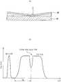
도 4(b)는 검출된 표면 탄성파의 포락선(envelope) 파형의 일례를 나타내는 그래프이다.Fig. 4B is a graph showing an example of an envelope waveform of the detected surface acoustic wave.
도 4(b)에서, 가로축은 시간을 나타내고, 세로축은 표면 탄성파의 신호 강도를 나타내고 있다.In Fig. 4B, the horizontal axis represents time and the vertical axis represents signal strength of surface acoustic waves.
여기서는, 도 3에 나타내는 X 송신자(51)로부터 표면 탄성파 Wvx가 터치 패널 기판(41)의 표면 상에 발신된 경우를 생각하고 있다.Here, the case where the surface acoustic wave Wvx is transmitted from the
X 송신자(51)로부터 발생한 표면 탄성파 Wvx는, 반사 배열(55, 57)을 경유하여, X 수신자(52)에 의해 검출된다.The surface acoustic wave Wvx generated from the
이 때, 반사 배열(55, 57)에 있어서의 각 반사 소자는, 다른 길이의 복수의 경로의 세트를 정한다.At this time, each reflecting element in the reflecting
반사 배열(55, 57)에 있어서의 연속하는 각 반사 소자가 반사하는 표면 탄성파 Wvx는, 점차로 길어지는 경로를 통해, X 수신자(52)에 도달한다.The surface acoustic waves Wvx reflected by each successive reflection element in the
그 때문에, 도 4(b)에 도시하는 바와 같이, X 수신자에 의해 검출된 수신 신호의 파형은, 발신 신호와 비교하여, 시간에 대하여 평평한 모양을 유지하는 사다리꼴 형상의 파형으로 된다.Therefore, as shown in Fig. 4B, the waveform of the received signal detected by the X receiver becomes a trapezoidal waveform that maintains a flat shape with respect to time as compared with the outgoing signal.
도 4(a)는 터치 패널의 터치 입력 상태의 단면도이다.4A is a cross-sectional view of a touch input state of a touch panel.
사용자가 손가락이나 펜 등으로 커버 필름(42)을 터치하면, 터치 입력 위치에서의 커버 필름(42)이 휘어, 터치 패널 기판(41)의 터치 입력면에 접촉한다.When the user touches the
터치 패널 기판(41) 상을 전파하는 표면 탄성파는, 커버 필름(42)이 접촉한 위치를 통과할 때, 커버 필름(42)에 의해 흡수되어 감쇠한다.The surface acoustic wave propagating on the
그 때문에, 도 4(b)에 나타내는 표면 탄성파 Wvx의 포락선 파형에는, 터치에 의한 신호의 결락(缺落)이 발생한다.Therefore, in the envelope waveform of surface acoustic wave Wvx shown to FIG. 4 (b), the signal fall by a touch generate | occur | produces.
수신 신호를 검출하고 나서, 이 터치에 의한 신호의 결락이 발생하기까지의 시간 Tg을 계측함으로써, 터치 입력 위치의 X 좌표를 특정할 수 있다.The X coordinate of the touch input position can be specified by measuring the time Tg from the detection of the received signal until the loss of the signal due to the touch occurs.
또, 터치 입력 위치의 Y 좌표를 특정하는 경우에 있어서도 마찬가지이다.The same applies to the case where the Y coordinate of the touch input position is specified.
이와 같이, 도 3에 나타내는 제어부(60)는, X 수신자(52)에 의해 검출된 표면 탄성파 Wvx와, Y 수신자(53)에 의해 검출된 표면 탄성파 Wvy를 기초로, 터치 입력 위치의 X 좌표 및 Y 좌표를 산출하도록 되어 있다.Thus, the
도 5는 제어부의 블럭도이다.5 is a block diagram of a control unit.
제어부(60)는, XY 송신자에 구동 신호를 출력하는 송신부와, XY 수신자로부터 수신 신호가 입력되는 수신부를 구비하고 있다.The
그 수신 신호는, 증폭기에 의해 증폭되고, 검파기에 의해 검파되어, A/D 변환기에 의해 양자화된다.The received signal is amplified by an amplifier, detected by a detector, and quantized by an A / D converter.
터치 패널 사용중에 있어서의 표면 탄성파의 수신 신호는, 양자화된 후에, 측정값으로서 제 1 RAM(62)에 저장된다.The received signal of the surface acoustic wave in use of the touch panel is quantized and then stored in the
그런데, 터치 패널 기판 상을 전파하는 표면 탄성파는, 상기한 바와 같이 커버 필름이 접촉한 위치를 통과할 때에 감쇠할 뿐만 아니라, 도 6(a)에 나타내는 스페이서(43)의 위치를 통과할 때에도 감쇠한다.By the way, the surface acoustic wave propagating on the touch panel substrate not only attenuates when passing through the position where the cover film is in contact as described above, but also attenuates when passing through the position of the
그 때문에 스페이서(43)의 위치에서도, 도 6(b)에 나타내는 수신 신호의 결락이 발생한다.Therefore, also in the position of the
그래서, 스페이서 위치에서의 수신 신호의 결락을 파악하기 위해, 터치 패널의 사용 준비(캘리브레이션) 작업으로서, 커버 필름을 누르지 않은 상태에서 표면 탄성파의 수신 신호를 측정해 놓는다.Then, in order to grasp | ascertain the lack of the received signal in a spacer position, as a preparation for use (calibration) of a touch panel, the received signal of a surface acoustic wave is measured without pressing a cover film.
그 수신 신호는, 양자화된 후에, 기준값으로서 도 5에 나타내는 제 2 RAM(63)(메모리)에 저장된다.After the received signal is quantized, it is stored in the second RAM 63 (memory) shown in Fig. 5 as a reference value.
또한, 도 5에 나타내는 제어부(60)는 ROM(61), 판단부(64), 및 통신부를 구비하고 있다.In addition, the
ROM(61)에는, 터치 입력 유무를 판단하는 임계값이 저장되어 있다.The
또한, 판단부(64)는, 제 1 RAM(62)에 저장된 측정값과, 제 2 RAM(63)에 저장된 기준값과의 차분을 얻는다.In addition, the
그 차분은, ROM(61)에 저장된 임계값을 넘은 부분을 터치 입력 위치로서 검출하는 것에 의해 얻어지는 값이다.The difference is a value obtained by detecting a portion beyond the threshold stored in the
또한, 통신부는 검출된 터치 입력 위치의 XY 좌표를 출력한다.In addition, the communication unit outputs the XY coordinates of the detected touch input position.
(터치 패널의 터치 입력 위치 검출 방법)(How to detect touch input position of touch panel)
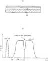
다음에, 터치 패널의 터치 입력 위치 검출 방법에 대하여 설명한다.Next, a touch input position detection method of the touch panel will be described.
도 7(a)∼도 7(c)는, 스페이서 위치의 근방이 터치 입력 위치로 되는 경우를 나타내고 있다.7A to 7C show a case where the vicinity of the spacer position becomes a touch input position.
도 7(a)는 단면도이며, 도 7(b)는 기준값 및 측정값의 신호 강도의 그래프이며, 도 7(c)는 측정값과 기준값과의 차분의 그래프이다.Fig. 7A is a sectional view, Fig. 7B is a graph of signal strengths of the reference value and the measured value, and Fig. 7C is a graph of the difference between the measured value and the reference value.
최초에, 터치 패널의 사용 준비(캘리브레이션) 작업으로서, 커버 필름을 누르지 않은 상태에서 표면 탄성파의 수신 신호를 측정한다.Initially, as a preparation for use (calibration) operation of the touch panel, the received signal of the surface acoustic wave is measured without pressing the cover film.
우선, 터치 패널 기판 상에 표면 탄성파가 송신되고, 스페이서의 위치에서 감쇠한 표면 탄성파가 수신되고, 또한, 제어부에 입력된다.First, a surface acoustic wave is transmitted on a touch panel substrate, a surface acoustic wave attenuated at the position of the spacer is received, and is also input to the controller.
이에 따라, 도 7(b)에 도시하는 바와 같이, 스페이서 위치에서의 신호 강도가 저하한 기준값(91)이 생성된다.As a result, as shown in Fig. 7B, the
이 기준값(91)을, 도 5에 나타내는 제 2 RAM(63)에 저장한다.This
다음에, 터치 패널 사용중에 터치 입력 위치의 검출을 행한다.Next, the touch input position is detected while the touch panel is in use.
우선, 도 7(a)에 나타내는 터치 패널 기판(41) 상에 표면 탄성파가 송신된다.First, surface acoustic waves are transmitted on the
그 표면 탄성파는, 스페이서(43)의 위치에 덧붙여, 커버 필름(42)이 터치 패널 기판(41)에 접촉한 위치(터치 입력 위치)에서 감쇠한다.The surface acoustic wave attenuates at the position (touch input position) in which the
그 표면 탄성파는 수신되어, 제어부에 입력된다.The surface acoustic wave is received and input to the controller.
이에 따라, 도 7(b)에 도시하는 바와 같이, 스페이서 위치 및 터치 입력 위치에서의 신호 강도가 저하한 측정값(92)이 생성된다.As a result, as shown in FIG. 7B, the measured
이 측정값(92)은 도 5에 나타내는 제 1 RAM(62)에 저장된다.This measured
다음에, 제어부(60)에 있어서의 판단부(64)는, 제 2 RAM(63)으로부터 기준값을 판독하고, 제 1 RAM(62)으로부터 측정값을 판독하며, 그리고 도 7(c)에 나타내는 양자의 차분(97)을 산출한다.Next, the
터치 입력 위치에서는, 기준값(91)에는 수신 강도의 저하가 없고, 측정값(92)의 수신 강도만이 저하하고 있기 때문에, 차분(97)이 유의로 된다.In the touch input position, the
이것에 대하여 스페이서 위치에서는, 기준값(91) 및 측정값(92)의 모두 수신 강도가 동등하게 저하하고 있기 때문에, 차분(97)은 거의 0으로 된다.On the other hand, at the spacer position, since the reception strength of the
다음에, 판단부는, 도 7(c)에 나타내는 차분(97)과, 미리 등록된 임계값(96)을 비교한다.Next, the determination unit compares the
그리고, 차분(97)이 임계값(96)을 넘은 경우에, 그 위치가 터치 입력 위치로서 검출된다.And when the
또, 임계값(96)으로서, 기준값 또는 측정값에 중첩하는 노이즈 레벨보다 큰 값을 설정해 두면, 터치 입력 위치의 오 검출을 저감할 수 있다.In addition, if the value greater than the noise level superimposed on the reference value or the measured value is set as the
이와 같이 본 실시예에서는, 터치 패널 기판 상에 스페이서가 세워져 마련되어 있기 때문에, 스페이서에 의한 감쇠량을 포함하는 표면 탄성파의 기준값을 측정할 수 있다.As described above, in the present embodiment, since the spacer is standing on the touch panel substrate, the reference value of the surface acoustic wave including the amount of attenuation by the spacer can be measured.
이에 따라, 터치 패널 사용중에 있어서의 상기 표면 탄성파의 측정값과 상기 기준값과의 차분은, 스페이서 위치에서 유의로 되지 않는다.Accordingly, the difference between the measured value of the surface acoustic wave and the reference value during use of the touch panel does not become significant at the spacer position.
이 때문에, 스페이서 위치를 터치 입력 위치로 판단하는 오 검출을 방지할 수 있다.For this reason, false detection which judges a spacer position as a touch input position can be prevented.
그런데, 종래의 터치 패널에서는, 터치 패널 기판에 대향하여, 탄성률이 높은 유리 기판이 배치되어 있었다.By the way, in the conventional touch panel, the glass substrate with high elasticity modulus was arrange | positioned facing the touch panel substrate.
이러한 유리 기판을 누르면, 도 7(a)에 도시하는 바와 같이, 터치 입력 위치의 근방에 배치된 스페이서(43)를, 동시에 강하게 누르게 된다.When such a glass substrate is pressed down, the
이에 따라, 도 7(b)에 나타내는 종래의 측정값(93)에 있어서는, 스페이서 위치에서의 신호 강도의 저하량이, 기준값(91)에 비해 커진다.As a result, in the conventional measured
그 때문에, 도 7(c)에 나타내는 종래의 차분(98)은, 누른 위치에 덧붙여 스페이서 위치에서도 유의가 된다.Therefore, the
이에 따라, 터치 입력 위치의 오 검출이 많이 발생한다는 문제가 있다.Accordingly, there is a problem that a large number of false detections of touch input positions occur.
또, 유리 기판을 누른 상태에서 도 7(b)에 나타내는 기준값(91)을 측정하면, 스페이서 위치에서의 신호 강도의 저하량이 종래의 측정값(93)과 동등해진다.Moreover, when the
그러나, 터치 패널 사용중과 마찬가지로 유리 기판을 누르는 것은 불가능하 며, 또한, 터치 패널의 사용 준비(캘리브레이션) 작업이 번잡해진다.However, it is impossible to press the glass substrate as in the use of the touch panel, and the preparation for use (calibration) of the touch panel is complicated.
이것에 비하여, 본 실시예의 터치 패널에서는, 터치 패널 기판에 대향하여, 탄성률이 낮은 커버 필름이 배치되어 있다.On the other hand, in the touch panel of this Example, the cover film with a low elastic modulus is arrange | positioned facing a touch panel board | substrate.
커버 필름은 가요성을 갖기 때문에, 스페이서 위치의 근방이 터치 입력 위치로 되더라도, 스페이서를 강하게 누르는 일이 없다.Since the cover film is flexible, even if the vicinity of the spacer position becomes the touch input position, the spacer is not pressed strongly.
그 때문에, 커버 필름을 누르지 않은 상태에서 표면 탄성파의 기준값을 측정하면 충분하게 되어, 터치 패널의 사용 준비(캘리브레이션) 작업을 간소화할 수 있다.Therefore, it is enough to measure the reference value of the surface acoustic wave in a state in which the cover film is not pressed, thereby simplifying the preparation for use (calibration) of the touch panel.
도 8(a)∼도 8(c)는, 스페이서 위치가 터치 입력 위치로 되는 경우를 도시하는 도면이다.8 (a) to 8 (c) are diagrams showing the case where the spacer position becomes the touch input position.
도 8(a)는 단면도이며, 도 8(b)는 기준값 및 측정값의 신호 강도의 그래프이며, 도 8(c)는 측정값과 기준값과의 차분의 그래프이다.Fig. 8A is a sectional view, Fig. 8B is a graph of signal strengths of the reference value and the measured value, and Fig. 8C is a graph of the difference between the measured value and the reference value.
도 8(a)에 도시하는 바와 같이, 스페이서(43)의 위치에서 커버 필름(42)을 누른 경우에 대하여 검토한다.As shown to Fig.8 (a), the case where the
이 경우, 도 8(b)에 나타내는 측정값(92)은, 스페이서 위치에서의 신호 강도의 저하량이, 기준값(91)에 비해 커진다.In this case, the measured
그 때문에, 도 8(c)에 나타내는 차분(97)은, 스페이서 위치에서 유의로 되어, 임계값(96)을 넘는다.Therefore, the
이에 따라, 스페이서 위치를 터치 입력 위치로서 검출할 수 있다.Accordingly, the spacer position can be detected as the touch input position.
그런데, 종래의 터치 입력 위치 검출 방법에 있어서는, 터치 패널 사용 전의 캘리브레이션에 의해 스페이서 위치를 미리 검출해두고, 스페이서 위치를 터치 입력 위치의 검출 대상으로부터 제외하고 있었다.By the way, in the conventional touch input position detection method, the spacer position was detected beforehand by the calibration before using a touch panel, and the spacer position was excluded from the detection object of a touch input position.
즉, 터치 패널 사용중에 스페이서 위치가 누르게 되더라도, 그 위치를 터치 입력 위치로서 검출할 수가 없었다.That is, even when the spacer position is pressed while the touch panel is in use, the position could not be detected as the touch input position.
이것에 비하여, 본 실시예의 터치 입력 위치 검출 방법에서는, 상술한 바와 같이 스페이서 위치를 터치 입력 위치로서 검출할 수 있다.On the other hand, in the touch input position detection method of the present embodiment, as described above, the spacer position can be detected as the touch input position.
이에 따라, 터치 입력 위치의 검출 정밀도를 향상시킬 수 있다.Thereby, the detection accuracy of a touch input position can be improved.
(실시예 2)(Example 2)
도 9는 실시예 2에 따른 전기 광학 장치의 설명도이며, 도 2의 A-A 선에 대응하는 부분에서의 단면도이다.FIG. 9 is an explanatory diagram of an electro-optical device according to
도 9에 나타내는 실시예 2에 따른 전기 광학 장치는, 실시예 1의 커버 필름 대신에, 액정 장치(1)의 화상 표시측의 편광판(28)이 배치되어 있다.In the electro-optical device according to the second embodiment shown in FIG. 9, the
또, 실시예 1과 마찬가지의 구성으로 되는 부분에 대해서는, 그 상세한 설명을 생략한다.In addition, about the part which becomes the structure similar to Example 1, the detailed description is abbreviate | omitted.
실시예 2에서는, 액정 장치(1)의 상부 기판(20)의 외측에, 터치 패널(50)의 터치 패널 기판(41)이 장착되어 있다.In Example 2, the touch panel board |
당해 터치 패널 기판(41)의 터치 입력면(41a)에 대향하여, 액정 장치(1)의 편광판(28)이 배치되어 있다.The
이 편광판(28)에 있어서는, 폴리비닐알콜(PVA) 등에 요오드를 도핑한 편광 필름이, 삼초산 셀룰로즈(TAC) 등으로 이루어지는 베이스 기판에 장착되어 있다.In this
따라서, 편광판(28)의 탄성률은 실시예 1의 커버 필름의 탄성률과 동등하게 되어 있다.Therefore, the elasticity modulus of the
이와 같이, 실시예 1의 커버 필름 대신에 편광판(28)을 배치한 경우에도, 실시예 1과 동일한 효과를 얻을 수 있다.Thus, also when the
또한, 실시예 2에서는 커버 필름이 삭감되기 때문에, 전기 광학 장치를 박형화할 수 있다.In addition, in Example 2, since a cover film is reduced, an electro-optical device can be thinned.
이것에 비하여 실시예 1에서는, 편광판으로서의 기능에 관계없이, 커버 필름의 재료를 적절히 선택할 수 있다.On the other hand, in Example 1, the material of a cover film can be selected suitably regardless of a function as a polarizing plate.
(실시예 3)(Example 3)
도 10은, 실시예 3에 따른 전기 광학 장치의 설명도이며, 도 2의 A-A 선에 대응하는 부분에서의 단면도이다.FIG. 10 is an explanatory diagram of an electro-optical device according to the third embodiment, and is a cross-sectional view at a portion corresponding to the line A-A in FIG. 2.
도 10에 나타내는 실시예 3에 따른 전기 광학 장치는, 액정 장치의 상부 기판(20)이 터치 패널 기판으로서 기능한다.In the electro-optical device according to the third embodiment shown in FIG. 10, the
또, 실시예 1 및 실시예 2와 동일한 구성으로 되는 부분에 대해서는, 그 상세한 설명을 생략한다.In addition, the detailed description is abbreviate | omitted about the part which becomes the structure same as Example 1 and Example 2. FIG.
실시예 3에 있어서는, 액정 장치(1)의 상부 기판(20)의 표면에, 표면 탄성파의 송신자, 반사 배열 및 수신자(모두 도시하지 않음)가 마련되어 있다.In Example 3, a transmitter, a reflection arrangement, and a receiver (all not shown) of surface acoustic waves are provided on the surface of the
또한, 상부 기판(20)의 표면에는, 스페이서(43)가 마련되어 있다.In addition, a
그리고, 실시예 2와 마찬가지로, 상부 기판(20)에 대향하여 편광판(28)이 배치되어 있다.And similarly to Example 2, the
이와 같이, 본 실시예에 있어서는, 액정 장치(1)의 상부 기판(20)을 터치 패널 기판으로서 기능시키고 있기 때문에, 전기 광학 장치를 박형화할 수 있다.As described above, in the present embodiment, since the
또, 상술한 스페이서(43)는, 액정 장치(1)에 있어서의 복수의 화소(4)의 경계 영역에 배치되어 있다.In addition, the
실시예 1에 있어서는, 스페이서를 소정 영역에 배치하기 위해서는, 터치 패널 기판에 위치를 맞추어 스페이서를 형성하고, 액정 장치에 위치를 맞추어 터치 패널을 장착해야 한다.In Example 1, in order to arrange | position a spacer in a predetermined area | region, it is necessary to form a spacer in alignment with a touch panel board | substrate, and to mount a touch panel in alignment with a liquid crystal device.
이것에 비하여, 실시예 3에서는, 액정 장치(1)에 위치를 맞추어 스페이서를 형성하면 된다.On the other hand, in Example 3, a spacer may be formed in alignment with the
따라서, 스페이서를 정밀하게 소정 영역에 배치하는 것이 가능해져, 스페이서에 기인하는 액정 장치의 개구율의 저하를 억제할 수 있다.Therefore, it becomes possible to arrange | position a spacer precisely in a predetermined | prescribed area, and the fall of the aperture ratio of the liquid crystal device resulting from a spacer can be suppressed.
(전자기기)(Electronics)
다음에, 실시예의 전기 광학 장치를 구비한 전자기기의 예에 대하여, 도 11을 이용하여 설명한다.Next, an example of an electronic apparatus provided with the electro-optical device of the embodiment will be described with reference to FIG.
도 11은 휴대전화의 사시도이다.11 is a perspective view of a mobile telephone.
상술한 전기 광학 장치는 휴대전화(300)의 액정 표시부를 구성하고 있다.The above-mentioned electro-optical device constitutes a liquid crystal display of the
또, 상술한 전기 광학 장치는, 휴대전화 이외에도 여러가지의 전자기기에 적 용할 수 있다.The above-described electro-optical device can be applied to various electronic devices in addition to mobile phones.
예컨대, 액정 프로젝터, 멀티미디어 대응 퍼스널 컴퓨터(PC) 및 엔지니어링 워크스테이션(EWS), 페이저, 워드프로세서, 텔레비젼, 뷰파인더형 또는 모니터 직시형의 비디오 테이프 레코더, 전자수첩, 전자탁상계산기, 카 내비게이션 장치, POS 단말, 터치 패널을 구비한 장치 등의 전자기기에, 상기의 전기 광학 장치를 적용하는 것이 가능하다.For example, liquid crystal projectors, multimedia compatible personal computers (PCs) and engineering workstations (EWS), pagers, word processors, televisions, viewfinder or monitor direct view video tape recorders, electronic organizers, electronic desk calculators, car navigation devices, It is possible to apply said electro-optical device to electronic devices, such as a POS terminal and the apparatus provided with a touchscreen.
어느 쪽의 경우에도, 상기의 전기 광학 장치는, 터치 입력 위치의 오 검출을 방지하는 것이 가능한 터치 패널을 구비하고 있기 때문에, 신뢰성이 높은 전자기기를 제공할 수 있다.In either case, since the electro-optical device includes a touch panel capable of preventing false detection of a touch input position, it is possible to provide a highly reliable electronic device.
또, 본 발명의 기술 범위는, 상술한 실시예에 한정되는 것이 아니라, 본 발명의 취지를 일탈하지 않는 범위에 있어서, 상술한 실시예에 여러 가지의 변경을 가한 것을 포함한다.In addition, the technical scope of this invention is not limited to the above-mentioned embodiment, Comprising: Various changes were added to the above-mentioned embodiment in the range which does not deviate from the meaning of this invention.
즉, 실시예에서 든 구체적인 재료나 구성 등은 그저 일례에 불과하고, 적절히 변경이 가능하다.That is, the specific material, the structure, etc. which were mentioned in the Example are only an example, and can be changed suitably.
예컨대, 상기 실시예에서는 패시브 매트릭스 방식의 액정 장치를 예로 하여 설명했지만, 스위칭 소자로서 박막 트랜지스터(Thin Film Transistor; TFT)나 박막다이오드(Thin Film Diode; TFD) 등을 이용한 액티브 매트릭스 방식의 액정 장치에 본 발명을 적용하는 것도 가능하다.For example, in the above embodiment, a passive matrix type liquid crystal device has been described as an example. It is also possible to apply the invention.
또한, 상기 실시예에서는 투과형의 액정 장치를 예로 하여 설명했지만, 반사형이나 반투과 반사형의 액정 장치에 본 발명을 적용하는 것도 가능하다.In addition, in the said embodiment, although the transmissive liquid crystal device was demonstrated as an example, it is also possible to apply this invention to a reflective or semi-transmissive reflective liquid crystal device.
또한, 화상 표시 장치로서, 상기 실시예에서는 액정 장치를 채용했지만, 액정 장치와 같이 전계에 의해 물질의 굴절율이 변화되어 광의 투과율을 변화시키는 전기 광학 효과를 갖는 장치 외에, 전기 에너지를 광학 에너지로 변환하는 장치 등을 채용하는 것도 가능하다.In addition, although the liquid crystal device was employed as the image display device in the above embodiment, the electrical energy is converted into optical energy in addition to the device having an electro-optic effect in which the refractive index of the material is changed by an electric field to change the transmittance of light, as in the liquid crystal device. It is also possible to employ a device or the like.
즉, 본 발명은, 액정 장치뿐만 아니라, 유기 EL(Electro-Luminescence) 장치나 무기 EL 장치, 플라즈마 디스플레이 장치, 전기 영동 디스플레이 장치, 전자 방출 소자를 이용한 표시 장치(Field Emission Display 및 Surface-Conduction Electron-Emitter Display 등) 등의 발광 장치 등에 있어서도, 널리 적용하는 것이 가능하다.That is, the present invention is not only a liquid crystal device, but also an organic EL (Electro-Luminescence) device, an inorganic EL device, a plasma display device, an electrophoretic display device, and a display device using an electron emission device (Field Emission Display and Surface-Conduction Electron-). Also in light emitting devices, such as an emitter display, etc., it is possible to apply widely.
본 발명에 의하면, 터치 입력 위치의 오 검출을 방지하는 것이 가능한 터치 패널, 및 그 터치 입력 위치 검출 방법을 제공할 수 있다.According to the present invention, it is possible to provide a touch panel capable of preventing false detection of a touch input position, and a touch input position detection method thereof.
Claims (7)
Translated fromKoreanApplications Claiming Priority (2)
| Application Number | Priority Date | Filing Date | Title |
|---|---|---|---|
| JPJP-P-2006-00009469 | 2006-01-18 | ||
| JP2006009469AJP2007193469A (en) | 2006-01-18 | 2006-01-18 | TOUCH PANEL, TOUCH INPUT POSITION DETECTING METHOD, ELECTRO-OPTICAL DEVICE, AND ELECTRONIC DEVICE |
Publications (2)
| Publication Number | Publication Date |
|---|---|
| KR20070076488Atrue KR20070076488A (en) | 2007-07-24 |
| KR100831487B1 KR100831487B1 (en) | 2008-05-22 |
Family
ID=37814281
Family Applications (1)
| Application Number | Title | Priority Date | Filing Date |
|---|---|---|---|
| KR1020070004373AExpired - Fee RelatedKR100831487B1 (en) | 2006-01-18 | 2007-01-15 | Touch panel, method for detecting touch input position, electro-optic device, and electronic device |
Country Status (6)
| Country | Link |
|---|---|
| US (1) | US20070165009A1 (en) |
| EP (1) | EP1818790A2 (en) |
| JP (1) | JP2007193469A (en) |
| KR (1) | KR100831487B1 (en) |
| CN (1) | CN101004655A (en) |
| TW (1) | TW200805126A (en) |
Cited By (1)
| Publication number | Priority date | Publication date | Assignee | Title |
|---|---|---|---|---|
| KR101322951B1 (en)* | 2009-03-27 | 2013-10-29 | 엘지디스플레이 주식회사 | Organic Light Emitting Display Device |
Families Citing this family (47)
| Publication number | Priority date | Publication date | Assignee | Title |
|---|---|---|---|---|
| JP2008040608A (en)* | 2006-08-02 | 2008-02-21 | Fujitsu Component Ltd | Surface acoustic wave system touch panel |
| JP4650699B2 (en)* | 2008-03-06 | 2011-03-16 | Necインフロンティア株式会社 | Input device, input method, and program |
| US8508495B2 (en) | 2008-07-03 | 2013-08-13 | Apple Inc. | Display with dual-function capacitive elements |
| JP5055231B2 (en)* | 2008-09-08 | 2012-10-24 | 株式会社ジャパンディスプレイイースト | Touch position detection method for touch panel |
| KR100930497B1 (en)* | 2008-11-14 | 2009-12-09 | 이성호 | Touch panel |
| US8217913B2 (en)* | 2009-02-02 | 2012-07-10 | Apple Inc. | Integrated touch screen |
| TWI570494B (en)* | 2009-04-17 | 2017-02-11 | 元太科技工業股份有限公司 | Touch electrophoretic display |
| TW201113787A (en)* | 2009-10-05 | 2011-04-16 | Au Optronics Corp | Touch display panel and display device |
| TWI422905B (en)* | 2009-10-28 | 2014-01-11 | Wintek Corp | Touch panel integrated in display |
| US8624878B2 (en)* | 2010-01-20 | 2014-01-07 | Apple Inc. | Piezo-based acoustic and capacitive detection |
| CN101901085A (en)* | 2010-07-07 | 2010-12-01 | 深圳创维-Rgb电子有限公司 | A Method of Improving the Stability of Infrared Touch System |
| TW201224899A (en)* | 2010-12-14 | 2012-06-16 | xiang-yu Li | Synchronization device for detecting induced electric field as capacitive touch position detection |
| US10198097B2 (en) | 2011-04-26 | 2019-02-05 | Sentons Inc. | Detecting touch input force |
| US9189109B2 (en) | 2012-07-18 | 2015-11-17 | Sentons Inc. | Detection of type of object used to provide a touch contact input |
| US9639213B2 (en) | 2011-04-26 | 2017-05-02 | Sentons Inc. | Using multiple signals to detect touch input |
| US9477350B2 (en) | 2011-04-26 | 2016-10-25 | Sentons Inc. | Method and apparatus for active ultrasonic touch devices |
| US11327599B2 (en) | 2011-04-26 | 2022-05-10 | Sentons Inc. | Identifying a contact type |
| TWI457681B (en)* | 2011-09-30 | 2014-10-21 | E Ink Holdings Inc | Electronic paper display |
| EP2780783B1 (en) | 2011-11-18 | 2022-12-28 | Sentons Inc. | Detecting touch input force |
| US10235004B1 (en)* | 2011-11-18 | 2019-03-19 | Sentons Inc. | Touch input detector with an integrated antenna |
| US11262253B2 (en) | 2017-08-14 | 2022-03-01 | Sentons Inc. | Touch input detection using a piezoresistive sensor |
| CN104169847B (en) | 2011-11-18 | 2019-03-12 | 森顿斯公司 | local haptic feedback |
| US9348468B2 (en) | 2013-06-07 | 2016-05-24 | Sentons Inc. | Detecting multi-touch inputs |
| KR101976067B1 (en)* | 2012-07-25 | 2019-05-09 | 삼성디스플레이 주식회사 | A display device providing touch emitting key unit |
| CN103576995A (en)* | 2012-07-31 | 2014-02-12 | 电子触控产品解决方案公司 | Touch sensitive display with acoustic isolation |
| TWI461896B (en)* | 2012-11-07 | 2014-11-21 | Chih Chung Lin | Photoelectric conversion touch panel |
| US10088936B2 (en)* | 2013-01-07 | 2018-10-02 | Novasentis, Inc. | Thin profile user interface device and method providing localized haptic response |
| US9336723B2 (en) | 2013-02-13 | 2016-05-10 | Apple Inc. | In-cell touch for LED |
| JP6266892B2 (en)* | 2013-04-01 | 2018-01-24 | シナプティクス・ジャパン合同会社 | Driver IC and display device |
| JP5567727B1 (en)* | 2013-09-17 | 2014-08-06 | 株式会社フジクラ | Electronic device and control method of electronic device |
| US9459715B1 (en) | 2013-09-20 | 2016-10-04 | Sentons Inc. | Using spectral control in detecting touch input |
| US9880671B2 (en)* | 2013-10-08 | 2018-01-30 | Sentons Inc. | Damping vibrational wave reflections |
| CN116560524B (en) | 2013-12-13 | 2024-10-01 | 苹果公司 | Integrated touch and display architecture for self-capacitance touch sensor |
| US10133382B2 (en) | 2014-05-16 | 2018-11-20 | Apple Inc. | Structure for integrated touch screen |
| US9063699B1 (en)* | 2014-09-02 | 2015-06-23 | Aevoe International Ltd. | Glass touch screen protector |
| JP6202443B2 (en)* | 2014-10-31 | 2017-09-27 | 日本電信電話株式会社 | Shield for touch screen, electronic device |
| US10048811B2 (en) | 2015-09-18 | 2018-08-14 | Sentons Inc. | Detecting touch input provided by signal transmitting stylus |
| JP6386484B2 (en) | 2016-01-19 | 2018-09-05 | ファナック株式会社 | Electrical device with foreign object detection panel |
| CN106293219B (en)* | 2016-08-03 | 2019-09-06 | 京东方科技集团股份有限公司 | A device with pressure touch function and its control method |
| US10908741B2 (en) | 2016-11-10 | 2021-02-02 | Sentons Inc. | Touch input detection along device sidewall |
| US10296144B2 (en) | 2016-12-12 | 2019-05-21 | Sentons Inc. | Touch input detection with shared receivers |
| US10126877B1 (en) | 2017-02-01 | 2018-11-13 | Sentons Inc. | Update of reference data for touch input detection |
| US10585522B2 (en) | 2017-02-27 | 2020-03-10 | Sentons Inc. | Detection of non-touch inputs using a signature |
| US11157115B2 (en)* | 2017-03-31 | 2021-10-26 | Apple Inc. | Composite cover material for sensitivity improvement of ultrasonic touch screens |
| US11580829B2 (en) | 2017-08-14 | 2023-02-14 | Sentons Inc. | Dynamic feedback for haptics |
| JP6908493B2 (en)* | 2017-10-11 | 2021-07-28 | ローム株式会社 | Touch panel control circuit, control method, touch-type input device using it, electronic device |
| FI20205146A1 (en)* | 2020-02-12 | 2021-08-13 | Aito Bv | A piezoelectric sensing device |
Family Cites Families (9)
| Publication number | Priority date | Publication date | Assignee | Title |
|---|---|---|---|---|
| DE69416960T2 (en)* | 1993-12-07 | 1999-08-19 | Seiko Epson Corp | Touch panel input device and method for generating input signals for an information processing device |
| JPH09203890A (en)* | 1996-01-25 | 1997-08-05 | Sharp Corp | LIQUID CRYSTAL DISPLAY DEVICE WITH INPUT FUNCTION, REFLECTION TYPE LIQUID CRYSTAL DISPLAY DEVICE WITH INPUT FUNCTION, AND METHODS OF MANUFACTURING THE SAME |
| KR20000009756A (en) | 1998-07-28 | 2000-02-15 | 윤종용 | Image display element |
| KR100356989B1 (en) | 1999-04-13 | 2002-10-18 | 주식회사 엘지씨아이 | Polarizer unified transparent conductive film, touch panel unified polarizer and flat panel display unified touch panel |
| US6366277B1 (en)* | 1999-10-13 | 2002-04-02 | Elo Touchsystems, Inc. | Contaminant processing system for an acoustic touchscreen |
| US6975305B2 (en)* | 2001-12-07 | 2005-12-13 | Nec Infrontia Corporation | Pressure-sensitive touch panel |
| JP2003280821A (en)* | 2002-03-26 | 2003-10-02 | Matsushita Electric Ind Co Ltd | Light transmissive touch panel |
| JP4093308B2 (en)* | 2002-11-01 | 2008-06-04 | 富士通株式会社 | Touch panel device and contact position detection method |
| JP4198527B2 (en)* | 2003-05-26 | 2008-12-17 | 富士通コンポーネント株式会社 | Touch panel and display device |
- 2006
- 2006-01-18JPJP2006009469Apatent/JP2007193469A/ennot_activeWithdrawn
- 2006-12-28EPEP06027002Apatent/EP1818790A2/ennot_activeWithdrawn
- 2007
- 2007-01-15KRKR1020070004373Apatent/KR100831487B1/ennot_activeExpired - Fee Related
- 2007-01-16CNCNA2007100017267Apatent/CN101004655A/enactivePending
- 2007-01-16TWTW096101636Apatent/TW200805126A/enunknown
- 2007-01-17USUS11/654,307patent/US20070165009A1/ennot_activeAbandoned
Cited By (1)
| Publication number | Priority date | Publication date | Assignee | Title |
|---|---|---|---|---|
| KR101322951B1 (en)* | 2009-03-27 | 2013-10-29 | 엘지디스플레이 주식회사 | Organic Light Emitting Display Device |
Also Published As
| Publication number | Publication date |
|---|---|
| TW200805126A (en) | 2008-01-16 |
| EP1818790A2 (en) | 2007-08-15 |
| CN101004655A (en) | 2007-07-25 |
| US20070165009A1 (en) | 2007-07-19 |
| KR100831487B1 (en) | 2008-05-22 |
| JP2007193469A (en) | 2007-08-02 |
Similar Documents
| Publication | Publication Date | Title |
|---|---|---|
| KR100831487B1 (en) | Touch panel, method for detecting touch input position, electro-optic device, and electronic device | |
| US7593067B2 (en) | Electro-optical device and electronic equipment having touch panel with resin having particular elastic modulus | |
| KR100870793B1 (en) | Touch panel, electro-optic device, and manufacturing method for electro-optic device | |
| KR100867057B1 (en) | Touch panel, electrooptical device, and electronic apparatus | |
| US8077162B2 (en) | Touch panel and display device | |
| JP5413937B2 (en) | Electro-optical device and electronic apparatus | |
| US20100296027A1 (en) | Display device | |
| JP2008009225A (en) | Display device and its manufacturing method | |
| CN100476709C (en) | Touch panels, electro-optical devices and electronic equipment | |
| JP2007200230A (en) | Touch panel, electro-optical device and electronic equipment | |
| JP2009003672A (en) | Touch panel device, electro-optical device, and electronic device | |
| JP2007264688A (en) | Touch panel, electro-optic device, and electronic appliance | |
| JP2006243428A (en) | Display device, display device manufacturing method, liquid crystal display device, liquid crystal display device manufacturing method, and electronic apparatus | |
| JP2007264686A (en) | Touch panel, electrooptical device and electronic equipment | |
| JP4613858B2 (en) | Touch panel, electro-optical device and electronic apparatus | |
| JP2006343920A (en) | Touch panel, electro-optical device and electronic apparatus | |
| JP2006343919A (en) | Electro-optical device and touch panel | |
| JP2006343918A (en) | Electro-optical device, touch panel, and touch panel control method | |
| JP2007264687A (en) | Touch panel, electrooptic device and electronic equipment |
Legal Events
| Date | Code | Title | Description |
|---|---|---|---|
| A201 | Request for examination | ||
| PA0109 | Patent application | St.27 status event code:A-0-1-A10-A12-nap-PA0109 | |
| PA0201 | Request for examination | St.27 status event code:A-1-2-D10-D11-exm-PA0201 | |
| PG1501 | Laying open of application | St.27 status event code:A-1-1-Q10-Q12-nap-PG1501 | |
| D13-X000 | Search requested | St.27 status event code:A-1-2-D10-D13-srh-X000 | |
| D14-X000 | Search report completed | St.27 status event code:A-1-2-D10-D14-srh-X000 | |
| E701 | Decision to grant or registration of patent right | ||
| PE0701 | Decision of registration | St.27 status event code:A-1-2-D10-D22-exm-PE0701 | |
| GRNT | Written decision to grant | ||
| PR0701 | Registration of establishment | St.27 status event code:A-2-4-F10-F11-exm-PR0701 | |
| PR1002 | Payment of registration fee | St.27 status event code:A-2-2-U10-U11-oth-PR1002 Fee payment year number:1 | |
| PG1601 | Publication of registration | St.27 status event code:A-4-4-Q10-Q13-nap-PG1601 | |
| PR1001 | Payment of annual fee | St.27 status event code:A-4-4-U10-U11-oth-PR1001 Fee payment year number:4 | |
| PR1001 | Payment of annual fee | St.27 status event code:A-4-4-U10-U11-oth-PR1001 Fee payment year number:5 | |
| FPAY | Annual fee payment | Payment date:20130502 Year of fee payment:6 | |
| PR1001 | Payment of annual fee | St.27 status event code:A-4-4-U10-U11-oth-PR1001 Fee payment year number:6 | |
| FPAY | Annual fee payment | Payment date:20140418 Year of fee payment:7 | |
| PR1001 | Payment of annual fee | St.27 status event code:A-4-4-U10-U11-oth-PR1001 Fee payment year number:7 | |
| FPAY | Annual fee payment | Payment date:20150417 Year of fee payment:8 | |
| PR1001 | Payment of annual fee | St.27 status event code:A-4-4-U10-U11-oth-PR1001 Fee payment year number:8 | |
| R18-X000 | Changes to party contact information recorded | St.27 status event code:A-5-5-R10-R18-oth-X000 | |
| FPAY | Annual fee payment | Payment date:20160418 Year of fee payment:9 | |
| PR1001 | Payment of annual fee | St.27 status event code:A-4-4-U10-U11-oth-PR1001 Fee payment year number:9 | |
| FPAY | Annual fee payment | Payment date:20170421 Year of fee payment:10 | |
| PR1001 | Payment of annual fee | St.27 status event code:A-4-4-U10-U11-oth-PR1001 Fee payment year number:10 | |
| LAPS | Lapse due to unpaid annual fee | ||
| PC1903 | Unpaid annual fee | St.27 status event code:A-4-4-U10-U13-oth-PC1903 Not in force date:20180516 Payment event data comment text:Termination Category : DEFAULT_OF_REGISTRATION_FEE | |
| PC1903 | Unpaid annual fee | St.27 status event code:N-4-6-H10-H13-oth-PC1903 Ip right cessation event data comment text:Termination Category : DEFAULT_OF_REGISTRATION_FEE Not in force date:20180516 | |
| P22-X000 | Classification modified | St.27 status event code:A-4-4-P10-P22-nap-X000 |