KR20070071658A - Manufacturing Method of Semiconductor Device - Google Patents
Manufacturing Method of Semiconductor DeviceDownload PDFInfo
- Publication number
- KR20070071658A KR20070071658AKR1020050135328AKR20050135328AKR20070071658AKR 20070071658 AKR20070071658 AKR 20070071658AKR 1020050135328 AKR1020050135328 AKR 1020050135328AKR 20050135328 AKR20050135328 AKR 20050135328AKR 20070071658 AKR20070071658 AKR 20070071658A
- Authority
- KR
- South Korea
- Prior art keywords
- photoresist
- polysilicon layer
- semiconductor device
- manufacturing
- forming
- Prior art date
- Legal status (The legal status is an assumption and is not a legal conclusion. Google has not performed a legal analysis and makes no representation as to the accuracy of the status listed.)
- Withdrawn
Links
- 239000004065semiconductorSubstances0.000titleclaimsabstractdescription22
- 238000004519manufacturing processMethods0.000titleclaimsabstractdescription12
- 229920002120photoresistant polymerPolymers0.000claimsabstractdescription55
- 238000000034methodMethods0.000claimsabstractdescription32
- 229910021420polycrystalline siliconInorganic materials0.000claimsabstractdescription23
- 229920005591polysiliconPolymers0.000claimsabstractdescription23
- 239000011347resinSubstances0.000claimsabstractdescription22
- 229920005989resinPolymers0.000claimsabstractdescription22
- 238000004140cleaningMethods0.000claimsabstractdescription19
- 125000002887hydroxy groupChemical group[H]O*0.000claimsabstractdescription19
- 229910052796boronInorganic materials0.000claimsabstractdescription10
- -1boron ionsChemical class0.000claimsabstractdescription9
- 239000000758substrateSubstances0.000claimsabstractdescription9
- 239000000203mixtureSubstances0.000claimsabstractdescription8
- 238000002955isolationMethods0.000claimsabstractdescription7
- 239000007943implantSubstances0.000claimsdescription6
- 150000002500ionsChemical class0.000claimsdescription4
- 239000007788liquidSubstances0.000claimsdescription3
- 239000000178monomerSubstances0.000claimsdescription3
- NIXOWILDQLNWCW-UHFFFAOYSA-MAcrylateChemical compound[O-]C(=O)C=CNIXOWILDQLNWCW-UHFFFAOYSA-M0.000claimsdescription2
- CERQOIWHTDAKMF-UHFFFAOYSA-MMethacrylateChemical compoundCC(=C)C([O-])=OCERQOIWHTDAKMF-UHFFFAOYSA-M0.000claimsdescription2
- 229920001577copolymerPolymers0.000claimsdescription2
- PPBRXRYQALVLMV-UHFFFAOYSA-NStyreneChemical groupC=CC1=CC=CC=C1PPBRXRYQALVLMV-UHFFFAOYSA-N0.000claims1
- 230000008021depositionEffects0.000claims1
- 238000004132cross linkingMethods0.000abstractdescription5
- 230000007547defectEffects0.000abstractdescription5
- 230000000052comparative effectEffects0.000description4
- 150000001875compoundsChemical class0.000description4
- 239000012528membraneSubstances0.000description4
- 239000012535impuritySubstances0.000description3
- 239000011248coating agentSubstances0.000description2
- 238000000576coating methodMethods0.000description2
- 238000005530etchingMethods0.000description2
- 238000002513implantationMethods0.000description2
- 238000009832plasma treatmentMethods0.000description2
- 238000005406washingMethods0.000description2
- ZOXJGFHDIHLPTG-UHFFFAOYSA-NBoronChemical compound[B]ZOXJGFHDIHLPTG-UHFFFAOYSA-N0.000description1
- 229910052810boron oxideInorganic materials0.000description1
- 239000000356contaminantSubstances0.000description1
- JKWMSGQKBLHBQQ-UHFFFAOYSA-Ndiboron trioxideChemical compoundO=BOB=OJKWMSGQKBLHBQQ-UHFFFAOYSA-N0.000description1
- 230000009977dual effectEffects0.000description1
- 238000005468ion implantationMethods0.000description1
- 238000000059patterningMethods0.000description1
- 238000000206photolithographyMethods0.000description1
Images


Classifications
- H—ELECTRICITY
- H01—ELECTRIC ELEMENTS
- H01L—SEMICONDUCTOR DEVICES NOT COVERED BY CLASS H10
- H01L21/00—Processes or apparatus adapted for the manufacture or treatment of semiconductor or solid state devices or of parts thereof
- H01L21/02—Manufacture or treatment of semiconductor devices or of parts thereof
- H01L21/02041—Cleaning
- H01L21/02057—Cleaning during device manufacture
- H01L21/02068—Cleaning during device manufacture during, before or after processing of conductive layers, e.g. polysilicon or amorphous silicon layers
- H—ELECTRICITY
- H01—ELECTRIC ELEMENTS
- H01L—SEMICONDUCTOR DEVICES NOT COVERED BY CLASS H10
- H01L21/00—Processes or apparatus adapted for the manufacture or treatment of semiconductor or solid state devices or of parts thereof
- H01L21/02—Manufacture or treatment of semiconductor devices or of parts thereof
- H01L21/027—Making masks on semiconductor bodies for further photolithographic processing not provided for in group H01L21/18 or H01L21/34
- H01L21/0271—Making masks on semiconductor bodies for further photolithographic processing not provided for in group H01L21/18 or H01L21/34 comprising organic layers
- H01L21/0273—Making masks on semiconductor bodies for further photolithographic processing not provided for in group H01L21/18 or H01L21/34 comprising organic layers characterised by the treatment of photoresist layers
- H—ELECTRICITY
- H01—ELECTRIC ELEMENTS
- H01L—SEMICONDUCTOR DEVICES NOT COVERED BY CLASS H10
- H01L21/00—Processes or apparatus adapted for the manufacture or treatment of semiconductor or solid state devices or of parts thereof
- H01L21/02—Manufacture or treatment of semiconductor devices or of parts thereof
- H01L21/04—Manufacture or treatment of semiconductor devices or of parts thereof the devices having potential barriers, e.g. a PN junction, depletion layer or carrier concentration layer
- H01L21/18—Manufacture or treatment of semiconductor devices or of parts thereof the devices having potential barriers, e.g. a PN junction, depletion layer or carrier concentration layer the devices having semiconductor bodies comprising elements of Group IV of the Periodic Table or AIIIBV compounds with or without impurities, e.g. doping materials
- H01L21/26—Bombardment with radiation
- H01L21/263—Bombardment with radiation with high-energy radiation
- H01L21/265—Bombardment with radiation with high-energy radiation producing ion implantation
- H01L21/266—Bombardment with radiation with high-energy radiation producing ion implantation using masks
Landscapes
- Engineering & Computer Science (AREA)
- Physics & Mathematics (AREA)
- Microelectronics & Electronic Packaging (AREA)
- General Physics & Mathematics (AREA)
- Manufacturing & Machinery (AREA)
- Computer Hardware Design (AREA)
- Condensed Matter Physics & Semiconductors (AREA)
- Power Engineering (AREA)
- High Energy & Nuclear Physics (AREA)
- Health & Medical Sciences (AREA)
- Toxicology (AREA)
- Photosensitive Polymer And Photoresist Processing (AREA)
- Cleaning Or Drying Semiconductors (AREA)
Abstract
Translated fromKoreanDescription
Translated fromKorean도 1a는 붕소 이온 임플란트 후 스트립(strip) 공정에서 손상된 폴리실리콘층의 표면을 보여주는 사진이다.Figure 1a is a photograph showing the surface of the polysilicon layer damaged in the strip (strip) process after the boron ion implant.
도 1b는 붕소 이온 임플란트 후 스트립 공정에서 깨끗하게 제거되지 않아 유발된 디펙트(KLA)를 보여주는 사진이다.Figure 1b is a photograph showing the defect (KLA) caused by a clean removal in the strip process after the boron ion implant.
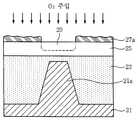
도 2a 내지 도 2e는 본 발명에 따른 반도체 소자의 제조 과정을 보여주는 모식도이다.2A to 2E are schematic views illustrating a manufacturing process of a semiconductor device according to the present invention.
도 3a는 실시예 1의 방법에 따라 형성된 폴리실리콘층의 표면 사진이다.3A is a surface photograph of a polysilicon layer formed according to the method of Example 1. FIG.
도 3b 및 도 3c는 각각 비교예 1 및 비교예 2의 방법에 따라 형성된 폴리실리콘층의 표면 사진이다.3B and 3C are photographs of the surface of the polysilicon layer formed according to the method of Comparative Example 1 and Comparative Example 2, respectively.
<도면의 주요 부분에 대한 부호 설명><Description of the symbols for the main parts of the drawings>
21 ; 반도체 기판, 21a ; 활성영역,21;
23 ; 소자분리막, 25 ; 폴리실리콘층,23; Device isolation film, 25; Polysilicon layer,
27 ; 포토레지스트 패턴, 27a ; 잔류 포토레지스트 패턴,27; Photoresist pattern, 27a; Residual photoresist pattern,
29 ; 불순물 주입 영역29; Impurity implantation area
본 발명은 반도체 소자의 제조 방법에 관한 것으로서, 보다 상세하게는 이온 주입 공정시 붕소 이온과 포토레지스트 수지 간에 가교결합이 형성됨으로 인해 후속 습식 세정 공정에서 세정이 잘 안되는 문제점을 해결할 수 있는 반도체 소자의 제조 방법에 관한 것이다.The present invention relates to a method for manufacturing a semiconductor device, and more particularly, because a crosslink is formed between boron ions and a photoresist resin during an ion implantation process, a semiconductor device capable of solving a problem of poor cleaning in a subsequent wet cleaning process. It relates to a manufacturing method.
반도체 소자의 듀얼 폴리 게이트(dual poly gate, DPG) 공정에 있어서, 붕소 임플란트(boron implant)시 KrF 또는 i-line 포토레지스트 내의 수산기(-OH)와 붕소 이온 사이의 반응으로 인한 가교화가 일어나게 되고, O2 가스로 제거하는 후속 공정에서 이들이 산화 붕소(boron oxide) 및 유기물의 찌꺼기를 형성하게 되는데, 상기 찌꺼기는 후속 습식 세정시에도 잘 제거되지 않기 때문에 디펙트(defect)의 원인이 되어 소자의 수율을 저하시키는 치명적인 원인이 되고 있다(도 1a 및 도 1b 참조). 따라서, 이와 같은 문제점을 해결하기 위해서는 식각 공정시 가능한 O2 가스를 사용하지 않거나, 또는 수산기가 없는 포토레지스트를 사용하여 붕소 이온과 포토레지스트 사이의 가교화 반응이 일어나는 원인을 제거함으로써 식각 후 후속 습식 세정 공정에서 상기 유기물 찌꺼기가 깨끗하게 제거될 수 있도록 하는 등의 방안이 요구되고 있다.In a dual poly gate (DPG) process of a semiconductor device, crosslinking occurs due to a reaction between hydroxyl groups (-OH) and boron ions in a KrF or i-line photoresist during a boron implant, In the subsequent process of removing with O2 gas, they form boron oxide and organic residues, which are difficult to remove even during the subsequent wet cleaning, causing defects and thus yield of the device. It is a fatal cause of lowering (see FIGS. 1A and 1B). Therefore, in order to solve such a problem, a subsequent wet process after etching is eliminated by eliminating the cause of the crosslinking reaction between the boron ions and the photoresist by using a photoresist without a possible O2 gas during the etching process or using a hydroxyl group without a hydroxyl group. There is a need for a method of allowing the organic residue to be removed cleanly in the cleaning process.
본 발명은 상기와 같은 종래 반도체 소자 제조 방법상의 문제점을 해결하기 위해 안출된 것으로서, 수산기를 포함하지 않는 포토레지스트를 사용하여 상기 가 교화 반응 원인을 제거함으로써 후속 습식 세정 공정에서 세정이 잘 되게 하여 소자의 디펙트를 크게 개선시킬 수 있는 반도체 소자의 제조 방법을 제공하는 것을 목적으로 한다.The present invention has been made to solve the above problems in the conventional semiconductor device manufacturing method, by removing the cause of the cross-linking reaction using a photoresist that does not contain a hydroxyl group so that the device is well cleaned in the subsequent wet cleaning process It is an object of the present invention to provide a method for manufacturing a semiconductor device, which can greatly improve the defect of the film.
상기 목적을 달성하기 위하여, 본 발명은In order to achieve the above object, the present invention
1) 반도체 기판상에 활성영역을 정의하는 소자분리막을 형성하는 단계;1) forming an isolation layer defining an active region on the semiconductor substrate;
2) 상기 반도체 기판상에 폴리실리콘층을 형성하는 단계;2) forming a polysilicon layer on the semiconductor substrate;
3) 수산기를 포함하지 않는 포토레지스트 수지를 포함하는 포토레지스트 조성물을 사용하여 상기 활성영역상에 위치하는 상기 폴리실리콘층 부분을 노출시키는 포토레지스트 패턴을 형성하는 단계;3) forming a photoresist pattern exposing a portion of the polysilicon layer located on the active region using a photoresist composition comprising a photoresist resin free of hydroxyl groups;
4) 상기 포토레지스트 패턴을 마스크로 상기 폴리실리콘층 내에 B3+ 이온을 임플란트시키는 단계;4) implanting B3+ ions into the polysilicon layer using the photoresist pattern as a mask;
5) 상기 포토레지스트 패턴을 O2 플라즈마를 이용하여 제거하는 단계; 및5) removing the photoresist pattern using O2 plasma; And
6) 통상의 세정액으로 상기 폴리실리콘층 표면을 세정하는 단계를 포함하는 반도체 소자의 제조 방법을 제공한다.6) provides a method of manufacturing a semiconductor device comprising the step of cleaning the surface of the polysilicon layer with a conventional cleaning solution.
도 2a 및 도 2b를 참조하면, 반도체 기판(21)상에 활성영역(21a)과 필드영역을 정의하는 소자분리막(23)을 형성한다. 그 후 소자분리막(23)이 형성된 반도체 기판(21) 상부에 게이트절연막(미도시)을 형성한 후, 그 위에 폴리실리콘층(25)을 증착한다. 이때, 상기 폴리실리콘층은 1,000 내지 5,000Å, 바람직하게는 2,000Å 전후의 두께이다.Referring to FIGS. 2A and 2B, an
도 2c를 참조하면, 상기 폴리실리콘층(25)상에 수산기를 포함하지 않는 포토레지스트 수지를 도포한 후, 통상의 포토리소그라피 공정 기술에 의해 노광 및 현상 공정을 거쳐 상기 포토레지스트막을 선택적으로 제거함으로써 상기 활성영역(21a)과 이 부분과 경계하는 소자분리막(23) 부분상에 형성되는 폴리실리콘층 부분을 노출시키는 포토레지스트 패턴(27)을 형성한다. 상기 포토레지스트 수지는 i-라인(line)용 포토레지스트 수지, KrF용 포토레지스트 수지 또는 ArF용 포토레지스트 수지인 것을 특징으로 하며, 상기 수산기를 포함하지 않는 포토레지스트 수지는 특별히 한정되는 것은 아니나, 스티렌계 모노머와 아크릴레이트계 또는 메타크릴레이트계 모노머의 공중합체를 사용하는 것이 바람직하다.Referring to FIG. 2C, by applying a photoresist resin containing no hydroxyl group on the
그 후, 상기 포토레지스트 패턴(27)을 마스크로 B3+ 불순물을 상기 폴리실리콘층(25)내에 임플란트시켜 불순물 주입영역(29)을 형성한다. 이때, 임플란트 공정은 B3+ 이온을 1×10¹⁵/㎠ 내지 5×10¹⁶/㎠, 바람직하게는 5×10¹⁵/㎠의 도우즈량에서 10 내지 100 keV, 바람직하게는 40 keV 정도의 이온화 에너지로 임플란트시킨다.Thereafter, a B3+ impurity is implanted into the
도 2d를 참조하면, O2 플라즈마 처리시에는 바람직하게는 O2와 N2를 7:3의 부피비로 혼합한 혼합가스를 이용하여 1×10¹⁵ 내지 5×10¹⁶/㎠ 범위의 도우즈량과 5 내지 30 keV 범위의 이온화 에너지로 100 내지 200초 동안 플라즈마 처리를 함으로 써 포토레지스트 패턴(27)을 제거하게 된다.Referring to FIG. 2D, in the O2 plasma treatment, a dose amount in the range of 1 × 10¹⁵ to 5 × 10¹⁶ / cm 2 may be obtained using a mixed gas in which O2 and N2 are mixed at a volume ratio of 7: 3. The
도 2e를 참조하면, 통상의 세정액으로 상기 폴리실리콘층(25) 표면을 세정함으로써 잔류 포토레지스트 패턴(27a)을 제거한다. 상기에서, 세정액은 일반적으로 사용하는 막의 종류에 따라 화합물의 종류도 달라지고, 세정시의 온도에 따라 막의 제거율도 다르게 할 수 있다. 즉, 세정 온도를 높이거나 세정액 조성물 내부의 화합물의 유량비를 높이면 막의 제거율이 증가하고, 반대로 세정 온도가 낮추거나 조성물내의 화합물의 유량비를 낮추게 되면 막의 제거율도 낮아진다. 그러므로, 원하는 제거량에 따라 세정 온도 및 화합물의 양을 적절히 조절함으로써 오염물질만을 제거할 수 있다.Referring to FIG. 2E, the surface of the
이하, 본 발명을 실시예에 의해 상세히 설명한다. 단, 하기 실시예는 본 발명을 예시하기 위한 것일 뿐, 본 발명의 내용이 하기 실시예에 의해 한정되는 것은 아니다.Hereinafter, the present invention will be described in detail by way of examples. However, the following examples are only for illustrating the present invention, and the content of the present invention is not limited by the following examples.
실시예 1. 수산기를 포함하지 않는 포토레지스트 수지를 이용한 공정Example 1. Process using photoresist resin that does not contain hydroxyl group
수산기를 포함하지 않는 KrF용 포토레지스트 조성물(동진 쎄미켐의 DHK-H150)을 사용하여 포토레지스트 패턴을 형성한 후, B3+ 이온을 주입하였다. 그 후, 통상의 방식으로 O2 가스가 포함된 플라즈마 기체를 사용하여 상기 포토레지스트 패턴를 제거한 결과, 포토레지스트 찌꺼기가 남아 있지 않고 깨끗하게 제거되었다(도 3a).After forming a photoresist pattern using a photoresist composition for KrF (DHK-H150 from Dongjin Semichem) which does not contain a hydroxyl group, B3+ ions were implanted. Thereafter, the photoresist pattern was removed using a plasma gas containing O2 gas in a conventional manner, and the photoresist residue was cleanly removed (FIG. 3A).
비교예 1. 수산기를 포함하는 포토레지스트 수지를 이용한 공정(1)Comparative Example 1. Process (1) using photoresist resin containing hydroxyl group
수산기를 포함하는 i-라인용 포토레지스트 조성물(JSR사의 IX-061, 코팅 두께: 1200nm)를 사용하여 포토레지스트 패턴을 형성한 후, 상기 실시예 1과 동일한 방식으로 포토레지스트 패턴을 제거한 결과, 포토레지스트 찌꺼기가 완전히 제거되지 않고 남아 있었다(도 3b).After forming a photoresist pattern using a photoresist composition for the i-line containing a hydroxyl group (IX-061, JSR Corporation, coating thickness: 1200nm), after removing the photoresist pattern in the same manner as in Example 1, The resist residue remained without being completely removed (FIG. 3B).
비교예 2. 수산기를 포함하는 포토레지스트 수지를 이용한 공정(2)Comparative Example 2. Process (2) using photoresist resin containing hydroxyl group
수산기를 포함하는 KrF용 포토레지스트 조성물(TOK사의 DP015, 코팅 두께: 1200nm)를 사용하여 패터닝을 한 후, 상기 실시예 1과 동일한 방식으로 포토레지스트 패턴을 제거한 결과, 포토레지스트 찌꺼기가 완전히 제거되지 않고 남아 있었다(도 3c).After patterning using a photoresist composition for KrF containing a hydroxyl group (TO015 DP015, coating thickness: 1200 nm), the photoresist pattern was removed in the same manner as in Example 1, and the photoresist residue was not completely removed. It remained (FIG. 3C).
상기에서 살펴본 바와 같이, 본 발명의 방법에서는 수산기를 포함하지 않는 포토레지스트 수지를 사용하여 패턴을 형성함으로써 붕소 이온과 포토레지스트 수지 내에 존재하는 수산기 간의 가교결합으로 인해 후속 습식 세정 공정에서 세정이 잘 안되는 문제점을 해결하여 소자의 디펙트를 크게 개선시킬 수 있다.As described above, in the method of the present invention, the pattern is formed using a photoresist resin that does not include a hydroxyl group, so that it is difficult to clean in a subsequent wet cleaning process due to the crosslinking between the boron ions and the hydroxyl groups present in the photoresist resin. The problem can be solved to greatly improve the defect of the device.
Claims (5)
Translated fromKoreanPriority Applications (1)
| Application Number | Priority Date | Filing Date | Title |
|---|---|---|---|
| KR1020050135328AKR20070071658A (en) | 2005-12-30 | 2005-12-30 | Manufacturing Method of Semiconductor Device |
Applications Claiming Priority (1)
| Application Number | Priority Date | Filing Date | Title |
|---|---|---|---|
| KR1020050135328AKR20070071658A (en) | 2005-12-30 | 2005-12-30 | Manufacturing Method of Semiconductor Device |
Publications (1)
| Publication Number | Publication Date |
|---|---|
| KR20070071658Atrue KR20070071658A (en) | 2007-07-04 |
Family
ID=38506767
Family Applications (1)
| Application Number | Title | Priority Date | Filing Date |
|---|---|---|---|
| KR1020050135328AWithdrawnKR20070071658A (en) | 2005-12-30 | 2005-12-30 | Manufacturing Method of Semiconductor Device |
Country Status (1)
| Country | Link |
|---|---|
| KR (1) | KR20070071658A (en) |
- 2005
- 2005-12-30KRKR1020050135328Apatent/KR20070071658A/ennot_activeWithdrawn
Similar Documents
| Publication | Publication Date | Title |
|---|---|---|
| JP5018307B2 (en) | Resist pattern thickening material, resist pattern forming method, semiconductor device and manufacturing method thereof | |
| US20100181656A1 (en) | Methods of eliminating pattern collapse on photoresist patterns | |
| KR101873727B1 (en) | Composition for forming fine resist pattern, and pattern formation method using same | |
| US8158332B2 (en) | Method of manufacturing a semiconductor device | |
| JP2016541119A (en) | DC overlay freeze | |
| KR100390918B1 (en) | a method for manufacturing of semiconductor memory device | |
| US7943521B2 (en) | Method for patterning a semiconductor device | |
| CN108957958A (en) | Lithographic patterning method | |
| US7144673B2 (en) | Effective photoresist stripping process for high dosage and high energy ion implantation | |
| US8518634B2 (en) | Cleaning process for semiconductor device fabrication | |
| TW541602B (en) | Semiconductor device production method | |
| CN100524040C (en) | Pattern forming method and method for manufacturing semiconductor device | |
| US20060122084A1 (en) | Composition for removing photoresist, method of removing photoresist and method of manufacturing a semiconductor device using the same | |
| KR20070071658A (en) | Manufacturing Method of Semiconductor Device | |
| KR100819647B1 (en) | Manufacturing Method of Semiconductor Device | |
| JP2009004478A (en) | Pattern forming method and semiconductor device manufacturing method | |
| EP0617455B1 (en) | Semiconductor device fabrication method | |
| JP4566861B2 (en) | Resist composition, method for forming resist pattern, semiconductor device and method for manufacturing the same | |
| KR20070071624A (en) | Manufacturing Method of Semiconductor Device | |
| US6291135B1 (en) | Ionization technique to reduce defects on next generation lithography mask during exposure | |
| KR100366624B1 (en) | Method for manufacturing semiconductor device using anti-reflective coating film | |
| CN107799417B (en) | Method for manufacturing transistor | |
| KR100527375B1 (en) | A developing method for eliminating defects in gate patterning process | |
| KR20050069709A (en) | Method for removing photoresist pattern | |
| KR20060023338A (en) | Exposure mask of semiconductor element and exposure method using the same |
Legal Events
| Date | Code | Title | Description |
|---|---|---|---|
| PA0109 | Patent application | Patent event code:PA01091R01D Comment text:Patent Application Patent event date:20051230 | |
| PG1501 | Laying open of application | ||
| PC1203 | Withdrawal of no request for examination | ||
| WITN | Application deemed withdrawn, e.g. because no request for examination was filed or no examination fee was paid |