KR20070071293A - LCD and its manufacturing method - Google Patents
LCD and its manufacturing methodDownload PDFInfo
- Publication number
- KR20070071293A KR20070071293AKR1020050134612AKR20050134612AKR20070071293AKR 20070071293 AKR20070071293 AKR 20070071293AKR 1020050134612 AKR1020050134612 AKR 1020050134612AKR 20050134612 AKR20050134612 AKR 20050134612AKR 20070071293 AKR20070071293 AKR 20070071293A
- Authority
- KR
- South Korea
- Prior art keywords
- pattern
- color filter
- insulating substrate
- forming
- liquid crystal
- Prior art date
- Legal status (The legal status is an assumption and is not a legal conclusion. Google has not performed a legal analysis and makes no representation as to the accuracy of the status listed.)
- Withdrawn
Links
Images


Classifications
- G—PHYSICS
- G02—OPTICS
- G02F—OPTICAL DEVICES OR ARRANGEMENTS FOR THE CONTROL OF LIGHT BY MODIFICATION OF THE OPTICAL PROPERTIES OF THE MEDIA OF THE ELEMENTS INVOLVED THEREIN; NON-LINEAR OPTICS; FREQUENCY-CHANGING OF LIGHT; OPTICAL LOGIC ELEMENTS; OPTICAL ANALOGUE/DIGITAL CONVERTERS
- G02F1/00—Devices or arrangements for the control of the intensity, colour, phase, polarisation or direction of light arriving from an independent light source, e.g. switching, gating or modulating; Non-linear optics
- G02F1/01—Devices or arrangements for the control of the intensity, colour, phase, polarisation or direction of light arriving from an independent light source, e.g. switching, gating or modulating; Non-linear optics for the control of the intensity, phase, polarisation or colour
- G02F1/13—Devices or arrangements for the control of the intensity, colour, phase, polarisation or direction of light arriving from an independent light source, e.g. switching, gating or modulating; Non-linear optics for the control of the intensity, phase, polarisation or colour based on liquid crystals, e.g. single liquid crystal display cells
- G02F1/133—Constructional arrangements; Operation of liquid crystal cells; Circuit arrangements
- G02F1/1333—Constructional arrangements; Manufacturing methods
- G02F1/1335—Structural association of cells with optical devices, e.g. polarisers or reflectors
- G02F1/133509—Filters, e.g. light shielding masks
- G02F1/133514—Colour filters
- G02F1/133516—Methods for their manufacture, e.g. printing, electro-deposition or photolithography
- G—PHYSICS
- G02—OPTICS
- G02F—OPTICAL DEVICES OR ARRANGEMENTS FOR THE CONTROL OF LIGHT BY MODIFICATION OF THE OPTICAL PROPERTIES OF THE MEDIA OF THE ELEMENTS INVOLVED THEREIN; NON-LINEAR OPTICS; FREQUENCY-CHANGING OF LIGHT; OPTICAL LOGIC ELEMENTS; OPTICAL ANALOGUE/DIGITAL CONVERTERS
- G02F1/00—Devices or arrangements for the control of the intensity, colour, phase, polarisation or direction of light arriving from an independent light source, e.g. switching, gating or modulating; Non-linear optics
- G02F1/01—Devices or arrangements for the control of the intensity, colour, phase, polarisation or direction of light arriving from an independent light source, e.g. switching, gating or modulating; Non-linear optics for the control of the intensity, phase, polarisation or colour
- G02F1/13—Devices or arrangements for the control of the intensity, colour, phase, polarisation or direction of light arriving from an independent light source, e.g. switching, gating or modulating; Non-linear optics for the control of the intensity, phase, polarisation or colour based on liquid crystals, e.g. single liquid crystal display cells
- G02F1/133—Constructional arrangements; Operation of liquid crystal cells; Circuit arrangements
- G02F1/1333—Constructional arrangements; Manufacturing methods
- G02F1/1335—Structural association of cells with optical devices, e.g. polarisers or reflectors
- G02F1/133509—Filters, e.g. light shielding masks
- G02F1/133512—Light shielding layers, e.g. black matrix
- G—PHYSICS
- G02—OPTICS
- G02F—OPTICAL DEVICES OR ARRANGEMENTS FOR THE CONTROL OF LIGHT BY MODIFICATION OF THE OPTICAL PROPERTIES OF THE MEDIA OF THE ELEMENTS INVOLVED THEREIN; NON-LINEAR OPTICS; FREQUENCY-CHANGING OF LIGHT; OPTICAL LOGIC ELEMENTS; OPTICAL ANALOGUE/DIGITAL CONVERTERS
- G02F1/00—Devices or arrangements for the control of the intensity, colour, phase, polarisation or direction of light arriving from an independent light source, e.g. switching, gating or modulating; Non-linear optics
- G02F1/01—Devices or arrangements for the control of the intensity, colour, phase, polarisation or direction of light arriving from an independent light source, e.g. switching, gating or modulating; Non-linear optics for the control of the intensity, phase, polarisation or colour
- G02F1/13—Devices or arrangements for the control of the intensity, colour, phase, polarisation or direction of light arriving from an independent light source, e.g. switching, gating or modulating; Non-linear optics for the control of the intensity, phase, polarisation or colour based on liquid crystals, e.g. single liquid crystal display cells
- G02F1/133—Constructional arrangements; Operation of liquid crystal cells; Circuit arrangements
- G02F1/1333—Constructional arrangements; Manufacturing methods
- G02F1/1335—Structural association of cells with optical devices, e.g. polarisers or reflectors
- G02F1/133526—Lenses, e.g. microlenses or Fresnel lenses
- G—PHYSICS
- G02—OPTICS
- G02F—OPTICAL DEVICES OR ARRANGEMENTS FOR THE CONTROL OF LIGHT BY MODIFICATION OF THE OPTICAL PROPERTIES OF THE MEDIA OF THE ELEMENTS INVOLVED THEREIN; NON-LINEAR OPTICS; FREQUENCY-CHANGING OF LIGHT; OPTICAL LOGIC ELEMENTS; OPTICAL ANALOGUE/DIGITAL CONVERTERS
- G02F1/00—Devices or arrangements for the control of the intensity, colour, phase, polarisation or direction of light arriving from an independent light source, e.g. switching, gating or modulating; Non-linear optics
- G02F1/01—Devices or arrangements for the control of the intensity, colour, phase, polarisation or direction of light arriving from an independent light source, e.g. switching, gating or modulating; Non-linear optics for the control of the intensity, phase, polarisation or colour
- G02F1/13—Devices or arrangements for the control of the intensity, colour, phase, polarisation or direction of light arriving from an independent light source, e.g. switching, gating or modulating; Non-linear optics for the control of the intensity, phase, polarisation or colour based on liquid crystals, e.g. single liquid crystal display cells
- G02F1/133—Constructional arrangements; Operation of liquid crystal cells; Circuit arrangements
- G02F1/1333—Constructional arrangements; Manufacturing methods
- G02F1/1335—Structural association of cells with optical devices, e.g. polarisers or reflectors
- G02F1/13356—Structural association of cells with optical devices, e.g. polarisers or reflectors characterised by the placement of the optical elements
- G02F1/133565—Structural association of cells with optical devices, e.g. polarisers or reflectors characterised by the placement of the optical elements inside the LC elements, i.e. between the cell substrates
Landscapes
- Physics & Mathematics (AREA)
- Nonlinear Science (AREA)
- Mathematical Physics (AREA)
- Chemical & Material Sciences (AREA)
- Crystallography & Structural Chemistry (AREA)
- General Physics & Mathematics (AREA)
- Optics & Photonics (AREA)
- Engineering & Computer Science (AREA)
- Manufacturing & Machinery (AREA)
- Liquid Crystal (AREA)
- Optical Filters (AREA)
Abstract
Translated fromKoreanDescription
Translated fromKorean도 1은 종래기술에 따른 액정표시소자의 분해도1 is an exploded view of a liquid crystal display device according to the prior art
도 2는 종래기술에 따른 액정표시소자의 대략적인 단면도2 is a schematic cross-sectional view of a liquid crystal display device according to the related art.
도 3은 종래기술에 따른 컬러필터 기판의 단면도Figure 3 is a cross-sectional view of a color filter substrate according to the prior art
도 4a ~ 도 4e는 종래기술에 따른 컬러필터 기판의 제조방법을 나타내는 단면도4A to 4E are cross-sectional views illustrating a method of manufacturing a color filter substrate according to the prior art.
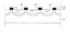
도 5는 본 발명에 따른 컬러필터 기판의 단면도5 is a cross-sectional view of a color filter substrate according to the present invention.
도 6a ~ 도 6f는 본 발명에 따른 컬러필터 기판 제조방법을 나타내는 단면도6A to 6F are cross-sectional views illustrating a method of manufacturing a color filter substrate according to the present invention.
** 도면의 주요부분에 대한 부호의 설명 **** Explanation of symbols for main parts of drawings **
203: 광굴절렌즈203: photorefractive lens
205a, 205b, 205c: 컬러필터 패턴205a, 205b, and 205c: color filter pattern
207: 블랙매트릭스207: Black Matrix
209: 오버코트층209: overcoat layer
211: 공통전극211: common electrode
213: 편광판213: polarizer
본 발명은 액정표시소자 및 그 제조방법에 관한 것으로, 특히 이웃한 화소간의 빛 섞임을 방지할 수 있는 액정표시소자 및 그 제조방법에 관한 것이다.BACKGROUND OF THE INVENTION 1. Field of the Invention The present invention relates to a liquid crystal display device and a method for manufacturing the same, and more particularly, to a liquid crystal display device and a method for manufacturing the same, which can prevent light mixing between adjacent pixels.
최근 디스플레이소자는 시각정보 전달매체로서 그 중요성이 한층 더 강조되고 있으며, 여러 가지 종류의 경쟁력 있는 디스플레이소자들이 많이 개발 되어지고 있다. 그러한 여러 가지 종류의 디스플레이소자 중에서 향후 주요한 위치를 점하기 위해서는 저소비전력화, 박형화, 경량화, 고화질화 등의 요건을 충족시켜야 한다.Recently, the importance of the display device as a visual information transmission medium has been further emphasized, and many kinds of competitive display devices have been developed. Among such various types of display devices, in order to occupy a major position in the future, it is necessary to satisfy requirements such as low power consumption, thinness, light weight, and high quality.
현재 평판 디스플레이(FPD: Flat Panel Display)의 주력 제품인 액정표시소자(LCD: Liquid Crystal Display)는 디스플레이의 이러한 조건들을 만족시킬 수 있는 성능뿐만 아니라 양산성까지 갖추었기 때문에, TV나 자동차용 네비게이션시스템 등 여러 응용분야에 널리 사용되고 있으며, 기존의 음극선관(Cathode Ray Tube; CRT)이 지배하고 있던 시장을 대체할 수 있는 핵심 디스플레이소자로서 자리 잡고 있다. Liquid crystal display (LCD), the flagship product of flat panel displays (FPDs), is not only capable of satisfying these conditions but also mass-produced. It is widely used in various applications and is positioned as a core display device that can replace the market dominated by a conventional cathode ray tube (CRT).
일반적으로, 액정표시소자는 매트릭스(matrix) 형태로 배열된 액정셀들에 외부에서 인가되는 화상정보에 따른 데이터신호를 개별적으로 공급하여, 상기 액정셀들의 광투과율을 조절함으로써 원하는 화상을 표시할 수 있도록 한 표시장치이다.In general, the liquid crystal display may display a desired image by individually supplying data signals according to image information applied from outside to liquid crystal cells arranged in a matrix form, and adjusting light transmittance of the liquid crystal cells. One display device.
이를 위하여 상기 액정표시소자의 액정패널은 크게 컬러필터(color filter) 기판과 박막트랜지스터 어레이 기판 및 상기 컬러필터 기판과 박막트랜지스터 어레이 기판 사이에 형성된 액정층(liquid crystal layer)으로 구성된다.To this end, the liquid crystal panel of the liquid crystal display device is largely composed of a color filter substrate, a thin film transistor array substrate, and a liquid crystal layer formed between the color filter substrate and the thin film transistor array substrate.
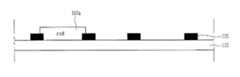
도 1은 일반적인 액정표시소자의 구성을 나타내는 도면으로, 이를 참조하여 액정표시소자를 구성하는 액정패널에 대하여 살펴보면 다음과 같다.FIG. 1 is a diagram illustrating a configuration of a general liquid crystal display device. Referring to the liquid crystal panel constituting the liquid crystal display device, the following description will be made.
도 1에 도시된 바와 같이, 일반적인 액정표시소자는 일반적으로 상판이라 불리우는 컬러필터 기판(113)과 하판인 박막트랜지스터 어레이 기판(101)과 액정층(109)으로 구성된다.As shown in FIG. 1, a general liquid crystal display device includes a
상기 컬러필터 기판은, 기판(113) 위에 컬러필터(117), 상기 각 컬러필터(117) 사이에 형성된 블랙매트릭스(BM : black matrix, 115) 및 상기 컬러필터(117)와 블랙매트릭스(115) 상부에 형성된 공통전극(111)으로 구성된다.The color filter substrate may include a
그리고 박막트랜지스터 어레이 기판은, 기판(101) 위의 화소영역(P)에 형성된 화소전극(107), 스위칭소자인 박막트랜지스터(TFT) 및 어레이배선(103, 105)으로 구성된다. 이 때, 박막 트랜지스터는 각 셀마다에 매트릭스형태(matrix type)로 위치하고, 이러한 다수의 박막 트랜지스터를 교차하여 지나가는 게이트배선(103)과 데이터배선(105)이 형성되며, 상기 게이트배선(103)과 데이터배선(105)이 교차하여 정의되는 영역에 화소영역(P)이 존재하고, 상기 화소영역(P)상에는 전술한 바와 같이, 투명한 도전층으로 구성된 화소전극(107)이 형성된다.The thin film transistor array substrate is composed of a
액정층은 상기 상판과 하판 사이에 형성되며, 광굴절률 이방성 성질을 가지는 액정물질(109)로 구성된다.The liquid crystal layer is formed between the upper plate and the lower plate, and is composed of a
그리고, 도 1에 도시되지는 않았지만 액정패널을 제외한 액정표시소자의 나머지 구성요소들을 살펴보면, 상기 액정패널의 양면에는 상판 및 하판에 각각 접촉하여 형성된 편광판이 구비되고, 상기 하판의 편광판 하부에는 램프 및 광학시트로 구성된 백라이트 유닛과 상기 액정패널을 지지하기 위한 탑 케이스 및 보텀 케이스 등이 구비되어 있다.Although not shown in FIG. 1, the remaining components of the liquid crystal display device other than the liquid crystal panel will be described. Both surfaces of the liquid crystal panel may include polarizing plates formed in contact with the upper and lower plates, respectively, under the polarizing plate of the lower plate. A backlight unit composed of an optical sheet, and a top case and a bottom case for supporting the liquid crystal panel are provided.
도 2는 편광판을 포함한 일반적인 액정패널의 개략적인 단면을 표시한 것으로서, 액정패널을 구성하는 하판인 박막트랜지스터 어레이 기판(101)의 하부 면과 상판인 컬러필터 기판(113)의 상부 면에 편광판(119a, 119b)이 각각 구비되어 있다. 이때, 상기 화소전극(107)은 개략적으로 도시되어 어레이 기판(101) 전면에 형성된 것처럼 보이지만, 실제로는 도 1에서 설명한 바와 같이 화소영역(도 1의 P)에 대응하여 각 화소(P)별로 형성되는 것이며, 도면에 도시되지는 않았지만 상기 화소전극(107)과 공통전극(111) 사이에는 액정이 충진되어 있다.FIG. 2 is a schematic cross-sectional view of a general liquid crystal panel including a polarizing plate, and a polarizing plate is formed on a lower surface of a thin film
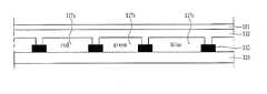
도 3은 컬러필터 기판에 편광판이 구비된 것을 나타내는 단면도로서, 이를 용하여 상판의 구조를 살펴보면 다음과 같다.3 is a cross-sectional view showing that a polarizing plate is provided in the color filter substrate, and looks at the structure of the upper plate using the following.
기판에 금속재료나 블랙수지로 이루어진 블랙매트릭스(115)가 화소영역의 주변을 따라 형성되며, 상기 블랙매트릭스(115) 사이에 순차적으로 적색, 녹색, 청색 컬러필터(117a, 117b, 117c)가 패턴을 형성한다.A
그리고 상기 컬러필터(117a, 117b, 117c) 위에 오버코트층(112)이 형성되며, 그 위에 인듐 틴 옥사이드(ITO : indium tin oxide)와 같은 투명한 도전층으로 이루어진 공통전극(111)이 형성되고, 이렇게 구성된 상기 컬러필터 기판의 하부면에 평광판(119a)이 부착된다.An
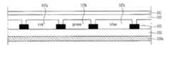
상기 컬러필터 기판의 대략적인 구조의 설명에 이어서, 컬러필터 기판의 제조 방법에 대해 도 4a ~도 4e를 참조하여 설명하면 다음과 같다.Following the description of the approximate structure of the color filter substrate, a method of manufacturing the color filter substrate will be described with reference to FIGS. 4A to 4E.
컬러필터 기판은, 일반적으로 정교성이 뛰어나고 재현성이 좋은 안료분산법에 의해 형성되고 있다.The color filter substrate is generally formed by the pigment dispersion method which is excellent in fineness and good reproducibility.
첫 번째 단계의 공정으로, 도 4a에 도시한 바와 같이, 기판(113) 위에 빛을 차단시킬 수 있는 금속물질 또는 블랙수지를 기판 전면에 형성한 후 사진식각기술을 이용하여 블랙매트릭스(115)의 패턴을 형성한다. 상기 블랙매트릭스(115)는, 하부기판의 화소전극 이외의 부분에서 발생하는 왜곡된 전계에 의하여 액정분자들이 비정상적인 배열을 하고 그 결과로 발생할 수 있는 빛샘 현상을 방지하는 역할을 하는 동시에, 박막 트랜지스터의 채널부로 빛이 입사되어 광전류가 발생하는 것을 방지하기 위함이다.In the first step, as shown in FIG. 4A, a metal material or black resin that can block light on the
다음 단계의 공정으로, 도 4b에 도시한 바와 같이, 상기 블랙매트릭스(115)가 형성된 기판(113)에 적색, 녹색, 청색 중의 한가지 색, 예를 들면 적색 컬러 리지스트를 스핀코팅 등의 방법을 통하여 기판(113) 전면에 도포하여 적색 리지스트층(116)을 형성한 후, 포토마스크(114)를 상기 기판(113) 위의 적색 리지스트층(116) 위에 얼라인(align)하여 위치시킨 후 노광을 한다.As a next step, as shown in FIG. 4B, one of red, green, and blue, for example, a red color resist is spin coated on the
다음 단계의 공정으로, 도 4c에 도시한 바와 같이, 상기 적색 리지스트층(도 4b의 116)을 현상하면, 상기 적색 리지스트층(도 4b의 116)은 네거티브(negative) 현상 특성을 가지고 있으므로, 빛을 받은 부분은 남게 되고, 빛을 받지 않은 부분은 제거되어 적색 컬러필터 패턴(117a)이 형성된다. 이후, 상기 적색 컬러필터 패턴(117a)을 경화시키기 위해 큐어링(curing)을 진행한다.In the next step, as shown in FIG. 4C, when the
다음 단계의 공정으로, 도 4d에 도시한 바와 같이, 나머지 녹색, 청색 컬러 필터 패턴(117b, 117c)을 형성하고, 오버코트층(112)과 공통전극(111)을 형성한다.In the next step, as shown in FIG. 4D, the remaining green and blue
상기 녹색, 청색 컬러필터 패턴(117b, 117c)은 상기 적색 컬러필터 패턴(117a)과 동일한 형성 방법으로 차례로 형성한다. 그리고 상기 적색, 녹색, 청색의 컬러필터 패턴(117a, 117b, 117c)를 포함하는 기판 전면에 투명 도전성 물질인 인듐 틴 옥사이드(ITO : indium tin oxide) 또는 인듐 징크 옥사이드(IZO : indium zinc oxide)를 증착하고, 사진식각기술을 이용하여 공통전극(111)을 형성한다. 이 때 상기 컬러필터 패턴(117a, 117b, 117c)과 공통전극(111) 사이에는 컬러필터 패턴(117a, 117b, 117c)의 보호와 단차 보상을 위해 BCB(benzo cyclo butene)로 이루어진 오버코트층(112)이 형성된다.The green and blue
마지막 단계의 공정으로, 도 4e에 도시된 바와 같이, 상기 컬러필터 기판의 하부면에 편광판(119a)을 부착한다. 상기 컬러필터 기판에 부착되는 편광판(119a)은 박막트랜지스터 어레이 기판의 하부면에 부착된 편광판(119b)와 함께 백라이트에서 공급된 빛의 투과를 조절하는 역할을 하게 된다.As a final step, as illustrated in FIG. 4E, the
상기 종래기술에 의하여 완성된 액정패널은 각 화소마다 구비된 스위칭소자인 박막트랜지스터에 의하여 독립적으로 구동되고, 각 화소들의 사이에는 블랙매트릭스가 구비되어 독립된 색을 구현하도록 설계되어 있다.The liquid crystal panel completed by the prior art is independently driven by a thin film transistor, which is a switching element provided for each pixel, and a black matrix is provided between each pixel to implement an independent color.
그러나, 상기 구조의 액정표시소자에서는 구현하는 색이 다른 인접한 셀에서는 다른 색의 빛이 섞여 표시될 수 있으며, 이렇게 빛이 섞이는 현상에 의하여 단위화소의 색순도가 떨어지는 문제점을 가지게 된다.However, in the liquid crystal display device having the above-described structure, light of different colors may be mixed and displayed in adjacent cells having different colors, and thus, the color purity of the unit pixel may be degraded due to the light mixing phenomenon.
본 발명의 다른 목적 및 특징들은 후술되는 발명의 구성 및 특허청구범위에 서 설명될 것이다.Other objects and features of the present invention will be described in the configuration and claims of the invention to be described later.
본 발명은 상기한 문제를 해결하기 위한 것으로, 본 발명에 따른 액정표시소자는 컬러필터 기판을 구성하는 컬러필터 패턴이 볼록렌즈 형태로 구성되며, 상기 컬러필터층 하부에 볼록렌즈 형태로 구성된 광굴절렌즈를 포함하여 이루어진다. 따라서 백라이트에서 발생된 빛이 상기 컬러필터 기판을 통과하며 각 단위화소의 중앙영역으로 집광되어, 인접한 화소간에 빛 섞임 현상을 방지하는 것을 목적으로 한다.The present invention is to solve the above problems, the liquid crystal display device according to the present invention is a color filter pattern constituting the color filter substrate is configured in the form of a convex lens, a photorefractive lens formed in the form of a convex lens below the color filter layer It is made, including. Therefore, the light generated from the backlight passes through the color filter substrate and is focused to the central area of each unit pixel, and the purpose is to prevent light mixing between adjacent pixels.
또한 상기 액정표시소자의 제조방법으로, 블랙매트릭스 패턴 형성 후에 절연기판을 습식 식각하여 그 하부를 오목하게 식각하고, 광굴절렌즈 형성시에도 화학기상증착법에서의 스텝커버리지(step coverage) 특성을 이용하여 컬러필터층과 광굴절렌즈를 각각 볼록렌즈 형태로 형성하는 것을 목적으로 한다.In addition, in the method of manufacturing the liquid crystal display device, after forming the black matrix pattern, the insulating substrate is wet-etched to concave the lower portion thereof, and the step coverage characteristic of the chemical vapor deposition method is used even when the photorefractive lens is formed. An object of the present invention is to form a color filter layer and a photorefractive lens in the form of a convex lens.
상기의 목적을 달성하기 위한 본 발명의 액정표시소자를 구성하는 컬러필터 기판은, 절연기판에 음각으로 형성된 소정의 패턴; 상기 음각으로 형성된 패턴의 내부에 채워진 적색, 녹색, 청색의 컬러필터 패턴; 상기 컬러필터 패턴 사이의 절연기판 위에 형성되어 매트릭스 형태로 패터닝된 블랙매트릭스; 및 상기 블랙매트릭스를 포함하는 기판 전면에 형성된 오버코트층을 포함하여 이루어진다.The color filter substrate constituting the liquid crystal display device of the present invention for achieving the above object comprises a predetermined pattern formed intaglio on the insulating substrate; A red, green, and blue color filter pattern filled in the intaglio-shaped pattern; A black matrix formed on an insulating substrate between the color filter patterns and patterned in a matrix; And an overcoat layer formed on the entire surface of the substrate including the black matrix.
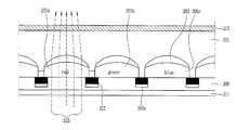
도 5는 본 발명에 따른 액정표시소자의 컬러필터 기판의 단면도로서, 이를 이용하여 그 구조를 설명하면 다음과 같다.5 is a cross-sectional view of a color filter substrate of a liquid crystal display device according to an exemplary embodiment of the present invention.
도 5에서는 빛의 진행 방향을 설명하기 위하여 컬러필터 기판의 상부층이 아래쪽으로 표시되어 있으나, 구조를 설명하기 위해서는 절연기판의 하부층에서 상부층의 순서로 설명하는 것이 편리하여 이에 따른다.In FIG. 5, the upper layer of the color filter substrate is shown downward to describe the direction of light travel. However, in order to explain the structure, it is convenient to explain the lower layer of the insulating substrate in the order of the upper layer.
먼저 유리와 같은 절연기판(201) 위에 소정의 음각형태의 패턴을 형성한다. 상기 소정의 음각 패턴은 하판인 박막트랜지스터 어레이 기판에 형성되는 화소영역에 대응하는 부분에 도트(dot) 형태로 구성되며, 그 하부는 오목하게 형성되는 것이 바람직하다.First, a predetermined intaglio pattern is formed on an insulating
상기 절연기판(201) 위에 형성된 음각형태의 패턴 내부에는 컬러필터 패턴(205a, 205b, 205c)이 형성된다. 상기 컬러필터 패턴(205a, 205b, 205c)은, 적색, 녹색, 청색으로 서로 다른 색을 나타내는 각 컬러필터 패턴이 서로 교차하는 순서로 연속적으로 배열되어 화면 표시를 위한 각 단위화소의 색을 결정한다.
이 때, 상기 컬러필터 패턴(205a, 205b, 205c)은 그 단면을 살펴보면 볼록렌즈의 형상을 하고 있다. 그 이유는 컬러필터 패턴(205a, 205b, 205c) 하부의 절연기판(201)이 상기에서 설명한 바에 따라 오목한 형상을 하고 있으며, 그 위에 형성되는 컬러필터 패턴(205a, 205b, 205c)은 하부의 단면 형상을 따라서 도포되고, 그 상부는 평탄하게 형성되기 때문이다. 한편, 상기 절연기판에 오목하게 형성된 음각 패턴의 내부에는 각각 투명층으로 이루어진 광굴절렌즈(203)가 형성될 수도 있다.At this time, the
이 때 상기 컬러필터 패턴(205a, 205b, 205c)과 광굴절렌즈(203)는 통상적인 유리기판의 굴절률인 1.5보다 큰 물질로 이루어져야 볼록렌즈로서의 기능을 수행하여 빛을 집속시킬 수 있다. 일반적으로 사용되는 컬러필터 재료의 굴절률은 1.5 이 상의 값을 가지므로 상기 볼록렌즈 기능 수행에 문제가 없으며, 상기 광굴절렌즈의 재료로는 약 2.5의 광굴절률을 가지는 DLC(diamond like carbon)가 사용될 수 있다.In this case, the
상기 컬러필터층(205a, 205b, 205c)과 광굴절렌즈(203)는 볼록렌즈의 형태로 구성되어, 굴절률이 서로 다른 매질 사이에서의 빛의 굴절특성상, 백라이트에서 발생한 빛(215)을 컬러필터 기판을 통과시키며 화소 중앙 영역으로 집광시킬 수 있다. 따라서, 종래기술에 따른 액정표시소자의 문제점이었던, 인접한 화소간의 빛 섞임 현상을 방지할 수 있다.The
계속하여 설명하면, 상기에서 설명한 컬러필터 패턴(205a, 205b, 205c) 사이의 음각되지 아니한 절연기판(201) 위에는 블랙매트릭스(207)가 형성된다. 상기 블랙매트릭스(207)는 각 화소영역의 테두리 부분에 형성되며, 하부 기판에 형성된 각종 배선에 인가되는 신호에 의하여 액정층에 불안정하게 발생하는 전계에 의한 크로스토크(cross-talk) 현상을 방지하는 역할을 한다. 이 때, 상기 블랙매트릭스(207)는 백라이트에서 발생한 빛을 차단시킬 수 있는 금속층이나 블랙수지로 이루어질 수 있고, 블랙매트릭스(207) 상부에는 광굴절렌즈를 구성하는 물질(203a)이 증착되어 있을 수도 있다.In the following description, a
이어서, 상기 블랙매트릭스(207)를 포함하는 기판 전면에 오버코트층(209)이 형성된다. 상기 오버코트층(209)은 BCB(benzo cyclo butene)로 구성될 수 있으며, 컬러필터 패턴(205a, 205b, 205c) 및 블랙매트릭스(207)를 보호하는 역할을 하고, 유기막의 코팅이므로 하부의 단차를 제거하는 역할도 수행한다.Subsequently, an
본 발명의 선택적 구성요소로서 공통전극(211)을 들 수 있다. 상기 선택적 구성요소인 공통전극(211)은 수평전계 방식의 액정표시소자에서는 박막트랜지스터 어레이 기판에 형성되므로 컬러필터 기판의 구성요소가 아니지만, 수직전계 방식의 액정표시소자에서는 컬러필터 기판에 형성되어야 할 구성요소가 된다. 수직전계 방식의 액정표시소자에서는 상기 오버코트층(209) 위에 인듐 틴 옥사이드(ITO : indium tin oxide)나 인듐 징크 옥사이드(IZO : indium zinc oxide)와 같은 투명한 도전체로 이루어진 공통전극(211)이 형성된다. 그리고 기판의 컬러필터 패턴을 포함한 면의 반대면에는 편광판(213)이 부착되어 있다.The
이로써 본 발명에 따른 액정표시소자를 구성하는 컬러필터 기판의 구조에 대하여 설명을 하였고, 이어서 도 6a ~ 도 6f를 참조하여 그 제조방법의 바람직한 실시예에 대하여 설명한다.Thus, the structure of the color filter substrate constituting the liquid crystal display device according to the present invention has been described. Next, a preferred embodiment of the manufacturing method will be described with reference to FIGS. 6A to 6F.
첫 번째 단계의 공정으로, 도 6a에 도시된 바와 같이 유리판과 같은 절연기판(201) 위에 블랙매트릭스(207) 패턴을 형성한다. 상기 공정은 크롬(Cr)과 같은 금속물질을 스퍼터링 등으로 증착하거나 블랙수지와 같이 빛을 효과적으로 차단시킬 수 있는 물질을 스핀코팅과 같은 방법으로 형성한 후, 사진식각기술을 이용하여 상기 층을 매트릭스 형태의 패턴으로 형성하는 것이다.In the first step, as shown in FIG. 6A, a
다음 단계의 공정으로, 도 6b에 도시된 바와 같이 상기 블랙매트릭스(207) 패턴을 마스크로 절연기판(201)을 식각한다. 이 때 상기 식각공정은 불산(HF)과 같은 식각제를 사용한 습식 식각 공정에 의하며, 식각된 패턴의 하부는 오목한 형태로 이루어진다. 그 이유는 습식 식각의 경우는 등방성 식각 특성을 보이며, 블랙매 트릭스 패턴과 식각제의 접촉각 특성으로 인하여 블랙매트릭스 사이의 넓은 공간에서의 식각률이 블랙매트릭스에서 가까운 부분에서의 식각률보다 크기 때문이다.In the next step, the insulating
다음 단계의 공정으로, 도 6c에 도시된 바와 같이 상기 절연기판(201)의 식각된 부분의 내부에 투명한 물질을 증착하여 광굴절렌즈(203)를 형성한다. 이 때 상기 투명한 물질은 DLC(diamond like carbon)와 같이 절연기판(201)보다 굴절률이 큰 물질이 선택되어야 하고, 화학기상증착법과 같은 방법에 의하여 형성된다. 화학기상증착법은 공정조건에 따라 평탄한 하부면에서의 증착률과 기울어진 하부면에서의 증착률이 달라지게 되는데, 평탄한 면에서의 증착률이 기울어진 하부면에서의 증착률보다 더 큰 것이 일반적이다.As a next step, as shown in FIG. 6C, a transparent material is deposited inside the etched portion of the insulating
따라서 화학기상증착법에 의하여 형성되는 투명물질은 화소영역의 중앙 부근에서는 두께가 두껍고, 가장자리로 갈수록 두께가 얇아져서 그 단면이 볼록렌즈의 형상을 하게 된다. 다만 상기 광굴절렌즈(203)를 형성하는 공정은 생략될 수도 있으며, 이 경우에는 후술될 컬러필터 패턴(도 6e의 205a, 205b, 205c)이 절연기판(201) 위에 직접 형성된다. 한편 광굴절렌즈(203) 형성 단계에서 상기 투명물질은 블랙매트릭스(207)의 상부에도 증착될 것이나(즉, 도면의 203a), 이는 액정표시소자의 동작과 무관하여 별도의 마스크를 사용하여 이를 방지할 필요성이 없다.Therefore, the transparent material formed by chemical vapor deposition has a thick thickness near the center of the pixel region, and becomes thinner toward the edge, thereby forming a convex lens in its cross section. However, the process of forming the
다음 단계의 공정으로, 도 6d에 도시된 바와 같이 상기 광굴절렌즈(203)가 형성된 절연기판(201)의 음각 패턴 내부에 적색, 녹색, 청색 컬러필터 패턴 중 하나, 즉 예를 들면 적색 컬러필터 패턴(205a)을 형성한다. 상기 공정은 종래기술에 서 설명한 안료분산법이나 최근에 연구가 많이 이루어지는 잉크젯(ink-jet)과 같은 방법에 의하여 이루어질 수 있다.As a next step, as shown in FIG. 6D, one of red, green, and blue color filter patterns, that is, for example, a red color filter is formed inside the intaglio pattern of the insulating
상기 컬러필터 패턴 형성 방법 중 안료분산법은, 적녹청의 색 중 어느 한 색을 구현하기 한 컬러 리지스트를 기판 전면에 도포한 후, 화소영역을 따라 패터닝된 포토마스크를 이용하여 도포된 상기 리지스트의 화소영역만을 노출시키고, 상기 노광에 의해 광화학적 구조가 변화된 상기 컬러 리지스트를 현상액에 담궈 패터닝하는 방법이다. 이 때, 일반적인 컬러 리지스트는 네거티브(negative) 리지스트의 성질을 가지므로 노광되지 않는 부분이 제거된다. 그리고, 상기 과정을 나머지 두 색을 가지는 컬러 리지스트에 대하여도 반복하여 적색, 녹색, 청색의 컬러필터 패턴을 완성한다.Pigment dispersion method of the color filter pattern forming method, after applying a color resist for implementing any one of the colors of red green cyan on the entire surface of the substrate, the ridge applied using a photomask patterned along the pixel area It is a method of exposing only the pixel region of the test strip and dipping the color resist whose photochemical structure has been changed by the exposure in a developer. In this case, since the general color resist has a negative resist property, an unexposed portion is removed. The above process is also repeated for the color resists having the remaining two colors to complete the color filter patterns of red, green, and blue.
이에 비하여 잉크젯에 의한 컬러필터 패턴 형성은, 패턴을 따라 기판 위에 배치된 잉크젯 분사장치가 각 화소영역에 해당 색의 컬러물질을 분사하게 되고, 분사된 적색, 녹색 및 청색의 컬러물질을 소정온도로 경화되어 컬러필터 패턴을 형성함으로서 이루어진다.On the other hand, in the color filter pattern formation by ink jet, the ink jet ejection apparatus disposed on the substrate along the pattern injects the color material of the corresponding color into each pixel area, and the ejected red, green, and blue color materials at a predetermined temperature. It is made by hardening | curing and forming a color filter pattern.
상기 방법 중 어느 방법을 이용하든지, 그 결과로 형성되는 컬러필터 패턴의 단면은 하부에서는 광굴절렌즈를 따라서 둥글게 형성되고, 상부는 중력에 의하여 평탄하게 형성된다.Whichever of the above methods is used, the resulting cross section of the color filter pattern is rounded along the photorefractive lens at the bottom and flat at the top by gravity.
다음 단계의 공정으로, 도 6e에 도시된 바와 적색 컬러필터 패턴(205a) 형성과 동일한 방법으로 나머지 색인 녹색, 청색 컬러필터 패턴(205b, 205c)을 형성한다. 이 때 노광에 사용되는 포토마스크는 적색 컬러필터 패턴(205a) 형성시에 사용 한 것과 동일한 포토마스크를 쉬프트(shift) 시켜서 사용한다.In the next step, the remaining index green and blue
다음 단계의 공정으로, 도 6f에 도시된 바와 같이 상기 적색, 녹색, 청색 컬러필터 패턴(205a, 205b, 205c)이 형성된 기판 전면에 오버코트층(209)을 형성한다. 상기 오버코트층(209)은 BCB(benzo cyclo butene)과 같은 유기물질을 스핀코팅과 같은 방법으로 형성한다.In the next step, an
그리고 수직전계형 액정표시소자에서는 공통전극이 컬러필터 기판 위에 형성되므로, 상기 오버코트층 형성 단계 이후에 인듐 틴 옥사이드(ITO : indium tin oxide)나 인듐 징크 옥사이드(IZO : indium zinc oxide)와 같은 투명한 도전체를 형성한 후 사진식각기술을 사용하여 공통전극(211)을 형성한다. 그리고 기판의 하부에는 편광판(213)이 부착된다.In the vertical field type liquid crystal display, since the common electrode is formed on the color filter substrate, a transparent conductor such as indium tin oxide (ITO) or indium zinc oxide (IZO) is formed after the overcoat layer forming step. After forming the
상기한 설명에 많은 사항이 구체적으로 기재되어 있으나 이것은 발명의 범위를 한정하는 것이라기보다 바람직한 실시예의 예시로서 해석되어야 한다. 따라서 발명은 설명된 실시예에 의하여 정할 것이 아니고 특허청구범위와 특허청구범위에 균등한 것에 의하여 정하여져야 한다.Many details are set forth in the foregoing description but should be construed as illustrative of preferred embodiments rather than to limit the scope of the invention. Therefore, the invention should not be defined by the described embodiments, but should be defined by the claims and their equivalents.
상술한 바와 같이, 본 발명에 따른 액정표시소자는 컬러필터 기판을 구성하는 컬러필터 패턴이 볼록렌즈 형태로 구성되어, 백라이트에서 발생된 빛을 컬러필터 기판을 통과시키며 각 단위화소의 중앙영역으로 집광시킬 수 있다. 또한 본 발명의 선택적 구성요소인 컬러필터층 하부에 볼록렌즈 형태로 구성된 광굴절렌즈에 의하여서도 컬러필터에 의한 것과 동일한 집광효과를 얻을 수 있다. 따라서 상기 집광효과에 의하여 종래기술에 따른 문제점이었던, 인접한 화소간에 빛 섞임 현상을 방지하는 효과를 가진다.As described above, in the liquid crystal display device according to the present invention, the color filter pattern constituting the color filter substrate is configured in the form of a convex lens so that light generated from the backlight passes through the color filter substrate and is focused on the central region of each unit pixel. You can. In addition, the same light condensing effect as that of the color filter can be obtained by the optical refraction lens formed in the convex lens type under the color filter layer, which is an optional component of the present invention. Therefore, the light condensing effect, which is a problem according to the prior art, has an effect of preventing light mixing between adjacent pixels.
또한 상기 액정표시소자의 제조방법은, 블랙매트릭스 패턴 형성 후에 절연기판을 습식 식각하는 과정에서 습식 식각의 등방성 식각 특성과 식각재와 식각되는 물질의 접촉각 특성을 이용하여 절연기판 하부를 오목하게 식각할 수 있다. 상기 현상에 의하여 볼록렌즈 형태의 컬러필터층의 형성이 가능하며, 광굴절렌즈 형성시에는 화학기상증착법의 스텝커버리지(step coverage) 특성을 이용하여 볼록렌즈 형태의 광굴절렌즈의 형성이 가능하다.In the method of manufacturing the liquid crystal display device, the lower portion of the insulating substrate may be concavely etched by using the isotropic etching characteristic of the wet etching and the contact angle characteristic of the material etched with the etching material in the process of wet etching the insulating substrate after the formation of the black matrix pattern. Can be. According to the above phenomenon, a convex lens-type color filter layer can be formed, and when forming a photorefractive lens, a convex lens-type photorefractive lens can be formed by using a step coverage characteristic of chemical vapor deposition.
Claims (14)
Translated fromKoreanPriority Applications (2)
| Application Number | Priority Date | Filing Date | Title |
|---|---|---|---|
| KR1020050134612AKR20070071293A (en) | 2005-12-29 | 2005-12-29 | LCD and its manufacturing method |
| US11/644,983US7489375B2 (en) | 2005-12-29 | 2006-12-26 | Liquid crystal display device and method of fabricating the same |
Applications Claiming Priority (1)
| Application Number | Priority Date | Filing Date | Title |
|---|---|---|---|
| KR1020050134612AKR20070071293A (en) | 2005-12-29 | 2005-12-29 | LCD and its manufacturing method |
Publications (1)
| Publication Number | Publication Date |
|---|---|
| KR20070071293Atrue KR20070071293A (en) | 2007-07-04 |
Family
ID=38223956
Family Applications (1)
| Application Number | Title | Priority Date | Filing Date |
|---|---|---|---|
| KR1020050134612AWithdrawnKR20070071293A (en) | 2005-12-29 | 2005-12-29 | LCD and its manufacturing method |
Country Status (2)
| Country | Link |
|---|---|
| US (1) | US7489375B2 (en) |
| KR (1) | KR20070071293A (en) |
Cited By (5)
| Publication number | Priority date | Publication date | Assignee | Title |
|---|---|---|---|---|
| WO2009093765A1 (en)* | 2008-01-22 | 2009-07-30 | Nak Hoon Seong | Color display pannel |
| US9406724B2 (en) | 2014-08-05 | 2016-08-02 | Samsung Display Co., Ltd. | Organic light-emitting diode (OLED) display with microlens below color filters and method of manufacturing the same |
| US9671640B2 (en) | 2013-07-24 | 2017-06-06 | Seiko Epson Corporation | Color filter substrate, electro-optical device, and projection-type display device |
| US9804434B2 (en) | 2015-02-02 | 2017-10-31 | Samsung Display Co., Ltd. | Liquid crystal display having shaped color filters |
| CN108196390A (en)* | 2018-01-02 | 2018-06-22 | 京东方科技集团股份有限公司 | Color membrane substrates and display device |
Families Citing this family (50)
| Publication number | Priority date | Publication date | Assignee | Title |
|---|---|---|---|---|
| KR101266396B1 (en)* | 2006-06-19 | 2013-05-22 | 삼성디스플레이 주식회사 | Color filter substrate, display panel having the same and method or making the same |
| JP2008281668A (en)* | 2007-05-09 | 2008-11-20 | Seiko Epson Corp | MICRO LENS SUBSTRATE WITH COLOR FILTER, ELECTRO-OPTICAL DEVICE, ELECTRONIC DEVICE, AND METHOD FOR MANUFACTURING MICRO LENS SUBSTRATE WITH COLOR FILTER |
| WO2010045364A1 (en)* | 2008-10-14 | 2010-04-22 | Real D | Lenticular display systems with offset color filter array |
| JP5420464B2 (en)* | 2010-04-02 | 2014-02-19 | オリンパス株式会社 | Display device, electronic device, portable electronic device, mobile phone, and imaging device |
| CN102707532B (en)* | 2011-05-13 | 2015-07-15 | 京东方科技集团股份有限公司 | Display |
| US9235057B2 (en) | 2012-05-18 | 2016-01-12 | Reald Inc. | Polarization recovery in a directional display device |
| US9188731B2 (en) | 2012-05-18 | 2015-11-17 | Reald Inc. | Directional backlight |
| US9678267B2 (en) | 2012-05-18 | 2017-06-13 | Reald Spark, Llc | Wide angle imaging directional backlights |
| KR102099590B1 (en) | 2012-05-18 | 2020-04-10 | 리얼디 스파크, 엘엘씨 | Controlling light sources of a directional backlight |
| EP2850488A4 (en) | 2012-05-18 | 2016-03-02 | Reald Inc | Directional backlight |
| WO2014050729A1 (en)* | 2012-09-28 | 2014-04-03 | シャープ株式会社 | Illumination device and display device |
| KR20140075979A (en)* | 2012-12-11 | 2014-06-20 | 삼성디스플레이 주식회사 | Liquid crystal display |
| CN111487707A (en) | 2013-02-22 | 2020-08-04 | 瑞尔D斯帕克有限责任公司 | directional backlight |
| CN103278873B (en)* | 2013-05-16 | 2016-08-10 | 深圳市华星光电技术有限公司 | Colorful filter structure and with the display panels of this colorful filter structure |
| KR102254799B1 (en) | 2013-06-17 | 2021-05-24 | 리얼디 스파크, 엘엘씨 | Controlling light sources of a directional backlight |
| KR102366346B1 (en) | 2013-10-14 | 2022-02-23 | 리얼디 스파크, 엘엘씨 | Light input for directional backlight |
| EP3058562A4 (en) | 2013-10-14 | 2017-07-26 | RealD Spark, LLC | Control of directional display |
| EP3161550A4 (en) | 2014-06-26 | 2018-04-18 | RealD Spark, LLC | Directional privacy display |
| KR102335812B1 (en)* | 2014-09-19 | 2021-12-09 | 삼성디스플레이 주식회사 | Organic light emitting diode device |
| CN104297832B (en)* | 2014-09-28 | 2017-02-15 | 合肥鑫晟光电科技有限公司 | Color filter, color filter manufacturing method, display panel, display device and driving method |
| WO2016057690A1 (en) | 2014-10-08 | 2016-04-14 | Reald Inc. | Directional backlight |
| US10356383B2 (en) | 2014-12-24 | 2019-07-16 | Reald Spark, Llc | Adjustment of perceived roundness in stereoscopic image of a head |
| RU2596062C1 (en) | 2015-03-20 | 2016-08-27 | Автономная Некоммерческая Образовательная Организация Высшего Профессионального Образования "Сколковский Институт Науки И Технологий" | Method for correction of eye image using machine learning and method of machine learning |
| WO2016168345A1 (en) | 2015-04-13 | 2016-10-20 | Reald Inc. | Wide angle imaging directional backlights |
| CN107850804B (en) | 2015-05-27 | 2021-06-11 | 瑞尔D斯帕克有限责任公司 | Wide-angle imaging directional backlight |
| US10475418B2 (en) | 2015-10-26 | 2019-11-12 | Reald Spark, Llc | Intelligent privacy system, apparatus, and method thereof |
| WO2017083526A1 (en) | 2015-11-10 | 2017-05-18 | Reald Inc. | Distortion matching polarization conversion systems and methods thereof |
| EP3374692B1 (en) | 2015-11-13 | 2021-02-24 | RealD Spark, LLC | Wide angle imaging directional backlights |
| WO2017083583A1 (en) | 2015-11-13 | 2017-05-18 | Reald Spark, Llc | Surface features for imaging directional backlights |
| CN114143495B (en) | 2016-01-05 | 2025-07-15 | 瑞尔D斯帕克有限责任公司 | Gaze Correction for Multi-View Images |
| EP3458897B1 (en) | 2016-05-19 | 2025-04-02 | RealD Spark, LLC | Wide angle imaging directional backlights |
| US10425635B2 (en) | 2016-05-23 | 2019-09-24 | Reald Spark, Llc | Wide angle imaging directional backlights |
| CN106501992B (en)* | 2017-01-03 | 2019-04-19 | 京东方科技集团股份有限公司 | A color filter substrate and a display panel |
| WO2018129059A1 (en) | 2017-01-04 | 2018-07-12 | Reald Spark, Llc | Optical stack for imaging directional backlights |
| US10600833B2 (en)* | 2017-03-01 | 2020-03-24 | Himax Technologies Limited | Image sensor |
| CN106773272A (en)* | 2017-03-06 | 2017-05-31 | 深圳市华星光电技术有限公司 | Colored optical filtering substrates and liquid crystal display panel |
| EP3607387A4 (en) | 2017-04-03 | 2020-11-25 | RealD Spark, LLC | Segmented imaging directional backlights |
| CN107221553A (en)* | 2017-06-01 | 2017-09-29 | 深圳市华星光电技术有限公司 | Improve the method and display panel of big visual angle colour cast |
| CN111183405A (en) | 2017-08-08 | 2020-05-19 | 瑞尔D斯帕克有限责任公司 | Adjust the digital representation of the head area |
| WO2019090246A1 (en) | 2017-11-06 | 2019-05-09 | Reald Spark, Llc | Privacy display apparatus |
| CN108563014A (en)* | 2018-01-10 | 2018-09-21 | 京东方科技集团股份有限公司 | Color membrane substrates and preparation method thereof and display device |
| KR102759510B1 (en) | 2018-01-25 | 2025-02-04 | 리얼디 스파크, 엘엘씨 | Touchscreen for privacy display |
| CN108628034B (en)* | 2018-05-25 | 2021-07-02 | 武汉华星光电技术有限公司 | Color film substrate, liquid crystal display panel and preparation method of color film substrate |
| CN110888270B (en)* | 2018-09-10 | 2021-04-30 | 京东方科技集团股份有限公司 | Display panel and display device |
| CN116194812A (en) | 2020-09-16 | 2023-05-30 | 瑞尔D斯帕克有限责任公司 | Vehicle Exterior Lighting |
| KR102791632B1 (en)* | 2020-12-31 | 2025-04-03 | 엘지디스플레이 주식회사 | Display apparatus |
| CN113782572B (en)* | 2021-09-09 | 2023-10-17 | 深圳市华星光电半导体显示技术有限公司 | Color film substrate, preparation method thereof and display panel |
| US11966049B2 (en) | 2022-08-02 | 2024-04-23 | Reald Spark, Llc | Pupil tracking near-eye display |
| WO2024035796A1 (en) | 2022-08-11 | 2024-02-15 | Reald Spark, Llc | Anamorphic directional illumination device |
| CN118151458B (en)* | 2024-05-10 | 2024-08-09 | 惠科股份有限公司 | Display panel and display device |
Family Cites Families (1)
| Publication number | Priority date | Publication date | Assignee | Title |
|---|---|---|---|---|
| WO2002099477A1 (en)* | 2001-06-01 | 2002-12-12 | Seiko Epson Corporation | Color filter and electro-optical device |
- 2005
- 2005-12-29KRKR1020050134612Apatent/KR20070071293A/ennot_activeWithdrawn
- 2006
- 2006-12-26USUS11/644,983patent/US7489375B2/enactiveActive
Cited By (9)
| Publication number | Priority date | Publication date | Assignee | Title |
|---|---|---|---|---|
| WO2009093765A1 (en)* | 2008-01-22 | 2009-07-30 | Nak Hoon Seong | Color display pannel |
| US9671640B2 (en) | 2013-07-24 | 2017-06-06 | Seiko Epson Corporation | Color filter substrate, electro-optical device, and projection-type display device |
| US9406724B2 (en) | 2014-08-05 | 2016-08-02 | Samsung Display Co., Ltd. | Organic light-emitting diode (OLED) display with microlens below color filters and method of manufacturing the same |
| US10084024B2 (en) | 2014-08-05 | 2018-09-25 | Samsung Display Co., Ltd. | Organic light-emitting diode (OLED) display and method of manufacturing the same |
| US10361253B2 (en) | 2014-08-05 | 2019-07-23 | Samsung Display Co., Ltd. | Organic light-emitting diode (OLED) display and method of manufacturing the same |
| US10608054B2 (en) | 2014-08-05 | 2020-03-31 | Samsung Display Co., Ltd. | Organic light-emitting diode (OLED) display and method of manufacturing the same |
| US9804434B2 (en) | 2015-02-02 | 2017-10-31 | Samsung Display Co., Ltd. | Liquid crystal display having shaped color filters |
| CN108196390A (en)* | 2018-01-02 | 2018-06-22 | 京东方科技集团股份有限公司 | Color membrane substrates and display device |
| CN108196390B (en)* | 2018-01-02 | 2021-10-15 | 京东方科技集团股份有限公司 | Color filter substrate and display device |
Also Published As
| Publication number | Publication date |
|---|---|
| US20070153160A1 (en) | 2007-07-05 |
| US7489375B2 (en) | 2009-02-10 |
Similar Documents
| Publication | Publication Date | Title |
|---|---|---|
| KR20070071293A (en) | LCD and its manufacturing method | |
| US7212262B2 (en) | Liquid crystal display device and method of fabricating the same | |
| US7126662B2 (en) | Transflective liquid crystal display device comprising a patterned spacer wherein the buffer layer and the spacer are a single body and method of fabricating the same | |
| JP5017289B2 (en) | Thin film patterning apparatus and color filter array substrate manufacturing method using the same | |
| US20100091234A1 (en) | Liquid Crystal Display Device | |
| US8908128B2 (en) | Color filter substrate and LCD device using it | |
| JP4048085B2 (en) | Color filter for liquid crystal and manufacturing method thereof | |
| KR101158872B1 (en) | Lquid Crystal Display and method for manufacturing the same | |
| US20050099580A1 (en) | Liquid crystal display device and method of fabricating the same | |
| US10802329B2 (en) | Colour filter, display apparatus and method for manufacturing colour filter | |
| US8675156B2 (en) | Color filter substrate for liquid crystal display, and manufacturing method thereof | |
| KR20030026736A (en) | Color Filter Panel for Liquid Crystal Display Device using Thermal Imaging and Method of Fabricating the same | |
| KR101112064B1 (en) | Manufacturing method of color filter substrate for liquid crystal display device | |
| JP2011107379A (en) | Color filter, method for manufacturing the same, and liquid crystal display panel using the same | |
| KR20070069829A (en) | LCD and its manufacturing method | |
| KR20080049252A (en) | Color filter substrate and its manufacturing method | |
| JP5028768B2 (en) | Color filter manufacturing method and liquid crystal display device | |
| KR20050008284A (en) | Liquid Crystal Display Panel And Fabricating Method Thereof | |
| JP4810713B2 (en) | Manufacturing method of color filter | |
| KR100749458B1 (en) | LCD with color filter formed on TF array and its manufacturing method | |
| KR101301515B1 (en) | LCD with color-filter on TFT and method of fabricating of the same | |
| KR101054326B1 (en) | LCD with color-filter on TFT and method of fabricating of the same | |
| JP2000284110A (en) | Color filter for liquid crystal, its production and liquid crystal display device | |
| KR101089097B1 (en) | Color filter substrate and liquid crystal display device using the same | |
| WO2006114933A1 (en) | Liquid crystal display device |
Legal Events
| Date | Code | Title | Description |
|---|---|---|---|
| PA0109 | Patent application | Patent event code:PA01091R01D Comment text:Patent Application Patent event date:20051229 | |
| PG1501 | Laying open of application | ||
| PC1203 | Withdrawal of no request for examination | ||
| WITN | Application deemed withdrawn, e.g. because no request for examination was filed or no examination fee was paid |