KR20070069754A - Memory modules - Google Patents
Memory modulesDownload PDFInfo
- Publication number
- KR20070069754A KR20070069754AKR1020050132210AKR20050132210AKR20070069754AKR 20070069754 AKR20070069754 AKR 20070069754AKR 1020050132210 AKR1020050132210 AKR 1020050132210AKR 20050132210 AKR20050132210 AKR 20050132210AKR 20070069754 AKR20070069754 AKR 20070069754A
- Authority
- KR
- South Korea
- Prior art keywords
- memory module
- memory
- chips
- guide grooves
- substrate
- Prior art date
- Legal status (The legal status is an assumption and is not a legal conclusion. Google has not performed a legal analysis and makes no representation as to the accuracy of the status listed.)
- Withdrawn
Links
Images


Classifications
- G—PHYSICS
- G06—COMPUTING OR CALCULATING; COUNTING
- G06F—ELECTRIC DIGITAL DATA PROCESSING
- G06F12/00—Accessing, addressing or allocating within memory systems or architectures
- G06F12/02—Addressing or allocation; Relocation
- G06F12/06—Addressing a physical block of locations, e.g. base addressing, module addressing, memory dedication
- G06F12/0615—Address space extension
- G06F12/0623—Address space extension for memory modules
- H—ELECTRICITY
- H01—ELECTRIC ELEMENTS
- H01L—SEMICONDUCTOR DEVICES NOT COVERED BY CLASS H10
- H01L25/00—Assemblies consisting of a plurality of semiconductor or other solid state devices
- H01L25/03—Assemblies consisting of a plurality of semiconductor or other solid state devices all the devices being of a type provided for in a single subclass of subclasses H10B, H10D, H10F, H10H, H10K or H10N, e.g. assemblies of rectifier diodes
- H01L25/10—Assemblies consisting of a plurality of semiconductor or other solid state devices all the devices being of a type provided for in a single subclass of subclasses H10B, H10D, H10F, H10H, H10K or H10N, e.g. assemblies of rectifier diodes the devices having separate containers
Landscapes
- Engineering & Computer Science (AREA)
- Physics & Mathematics (AREA)
- General Physics & Mathematics (AREA)
- Theoretical Computer Science (AREA)
- Power Engineering (AREA)
- Microelectronics & Electronic Packaging (AREA)
- General Engineering & Computer Science (AREA)
- Condensed Matter Physics & Semiconductors (AREA)
- Computer Hardware Design (AREA)
- Combinations Of Printed Boards (AREA)
Abstract
Translated fromKoreanDescription
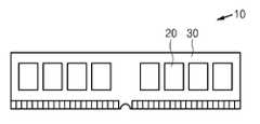
Translated fromKorean도 1은 종래의 메모리 모듈을 나타낸 평면도,1 is a plan view showing a conventional memory module,
도 2는 본 발명의 일 실시예에 따른 메모리 모듈을 나타낸 사시도,2 is a perspective view showing a memory module according to an embodiment of the present invention;
도 3은 도 2의 메모리 모듈 중 기판을 나타낸 사시도,3 is a perspective view illustrating a substrate in the memory module of FIG. 2;
도 4는 도 2의 메모리 모듈 중 패드 재배열 칩을 나타낸 단면도,4 is a cross-sectional view illustrating a pad rearrangement chip of the memory module of FIG. 2;
도 5는 도 2의 메모리 모듈 중 가이드 홈에 패드 재배열 칩이 결합된 모습을 나타낸 평면도,5 is a plan view illustrating a pad rearrangement chip coupled to a guide groove of the memory module of FIG. 2;
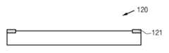
도 6은 도 2의 메모리 모듈 중 가이드 홈에 패키지가 결합된 모습을 나타낸 단면도.6 is a cross-sectional view illustrating a package coupled to a guide groove of the memory module of FIG. 2.
<도면의 주요부분에 대한 부호의 설명><Description of the symbols for the main parts of the drawings>
100... 메모리 모듈 110... 기판100 ...
111... 베이스 플레이트 112... 가이드 레일111 ...
113... 가이드 홈 114... 인터 커넥터113 ...
120... 패드 재배열 칩 121... 패드120 ... pad rearranged
본 발명은 메모리 모듈에 관한 것으로서, 특히 기판 상에 칩이 결합되는 구조가 변경된 메모리 모듈에 관한 것이다.BACKGROUND OF THE INVENTION 1. Field of the Invention The present invention relates to a memory module, and more particularly, to a memory module in which a structure in which chips are coupled on a substrate is changed.
일반적으로 메모리 모듈은 개인용 컴퓨터나 대용량 Workstation 등의 기억 용량을 확장 시키기 위해 다수의 메모리 칩을 하나의 인쇄회로기판 상에 평면 배치 구조로 고밀도 실장하여, 메모리 용량을 확장시킨 제품으로 SIMM (Single In-line Memory Module)과 DIMM (Dual In- line Memory Module), 그리고 최근에 개발된 RIMM (Rambus In-line Memory Module) 등이 있다.In general, the memory module is a product that expands the memory capacity by mounting a large number of memory chips in a flat layout structure on a single printed circuit board in order to expand the storage capacity of a personal computer or a large-capacity workstation. line memory modules (DIMMs), dual in-line memory modules (DIMMs), and the recently developed Rambus In-line Memory Modules (RIMMs).
그런데, 도 1과 같이 개인용 컴퓨터의 마더 보드(40) 상에 종래의 평면 배치 구조를 갖는 메모리 모듈(10)을 장착하기 위하여는 마더 보드(40) 상에 메모리 모듈(10) 크기만큼의 넓은 표면적이 요구되어, 결국 개인용 컴퓨터의 부피를 증가시키게 되고, 또한 메모리 모듈(10)을 구성 후, 일부의 메모리 칩(30)에서 불량이 발생할 경우, 메모리 칩(30)이 기판(20) 상에 결합된 상태이므로, 불량이 발생한 메모리 칩(30)만을 교체하기가 어려운 문제점이 있다.However, in order to mount the
본 발명은 상기의 문제점을 해결하기 위하여 창출된 것으로서, 메모리 모듈의 표면적을 줄여 공간 확보를 용이하게 하고, 메모리 칩 중 일부에 불량이 발생한 경우, 용이하게 교체할 수 있는 개선된 메모리 모듈을 제공하는 것을 그 목적으로 한다.SUMMARY OF THE INVENTION The present invention has been made to solve the above problems, and reduces the surface area of a memory module to facilitate space securing, and provides an improved memory module that can be easily replaced in the event of a failure of some of the memory chips. For that purpose.
상기의 목적을 달성하기 위한 본 발명의 메모리 모듈은, RLC 회로가 마련된 베이스 플레이트와, 상기 베이스 플레이트 양 단부 각각에 마련되고, 상기 RLC 회로와 전기적으로 연결되며, 다수의 가이드 홈이 형성된 가이드 레일을 구비한 기판; 및 상기 다수의 가이드 홈 각각에 삽입되는 다수의 패드 재배열 칩을 포함한 것이 바람직하다.The memory module of the present invention for achieving the above object, the base plate is provided with an RLC circuit, a guide rail provided at each end of the base plate, electrically connected to the RLC circuit, the guide rail formed with a plurality of guide grooves A substrate; And a plurality of pad rearrangement chips inserted into each of the plurality of guide grooves.
여기서, 상기 가이드 홈에는 상기 패드와 접촉되는 다수의 인터 커넥터가 마련된 것이 바람직하다.Here, the guide groove is preferably provided with a plurality of inter connectors in contact with the pad.
이하 첨부된 도면을 참조하면서 본 발명의 바람직한 실시예를 상세히 설명하기로 한다.Hereinafter, exemplary embodiments of the present invention will be described in detail with reference to the accompanying drawings.
도 2는 본 발명의 일 실시예에 따른 메모리 모듈을 나타낸 사시도이고, 도 3은 도 2의 메모리 모듈 중 기판을 나타낸 사시도이고, 도 4는 도 2의 메모리 모듈 중 메모리 칩을 나타낸 단면도이며, 도 5는 도 2의 메모리 모듈 중 가이드 홈에 패드 재배열 칩이 결합된 모습을 나타낸 평면도이다.2 is a perspective view illustrating a memory module according to an exemplary embodiment of the present invention, FIG. 3 is a perspective view illustrating a substrate of the memory module of FIG. 2, and FIG. 4 is a cross-sectional view illustrating a memory chip of the memory module of FIG. 2. 5 is a plan view illustrating a pad rearrangement chip coupled to a guide groove in the memory module of FIG. 2.
도면을 참조하면, 메모리 모듈(100)은 기판(110)과 다수의 패드 재배열 칩(120)을 포함한다.Referring to the drawing, the
기판(110)은 RLC 회로가 형성된 베이스 플레이트(111)와, 이 베이스 플레이트(111) 양측단부 상에 각각 마련된 한 쌍의 가이드 레일(112)을 포함한다.The
가이드 레일(112)은 베이스 플레이트(111)에 형성된 RLC회로와 전기적으로 연결되며, 이 한 쌍의 가이드 레일(112)에서 서로 마주보는 면에는 다수의 가이드 홈(113)이 형성된다.The
이 가이드 홈(113)으로는 패드 재배열 칩(120)이 슬라이딩 삽입되며, 패드 재배열 칩(120)에 마련된 패드(121)와 기판(110) 사이의 전기적 연결을 위하여 가이드 홈(113)에는 다수의 인터 커넥터(114)가 마련된다.The
물론, 이 인터 커넥터(114)는 베이스 플레이트(111)의 RLC 회로와 전기적으로 도통된다.Of course, this
패드 재배열 칩(120)은 양측단부 상에 재배열된 패드(121)가 마련되며, 가이드 홈(113)에 세로로 슬라이딩 삽입되어, 기판(110)과 전기적으로 연결된다.The
한편, 도 6과 같이 평면 기판 상에 본딩 패드가 마련된 패키지를 가이드 홈에 삽입할 수도 있다.Meanwhile, as illustrated in FIG. 6, a package in which a bonding pad is provided on a flat substrate may be inserted into a guide groove.
이와 같은 구조의 메모리 모듈(100)은 다수의 패드 재배열 칩(120)이 기판(110)의 가이드 홈(113)에 세로로 삽입되어, 메모리 용량은 증가시키면서, 메모리 모듈(100) 전체의 부피는 종래 평면 배치 방식보다 줄어들게 하므로, 마더 보드에 메모리 모듈(100)을 실장 시, 마더 보드에서의 점유 공간이 줄어들게 되어 제품의 소형화에 부응할 수 있게 되고, 또한 다수의 패드 재배열 칩(120) 중 일부가 파손 등의 불량이 발생한 경우, 가이드 홈(113)에서 빼내어 새로운 패드 재배열 칩(120)으로 교체하면 되므로, 생산성 및 경제성을 향상시킬 수 있게 된다.In the
상술한 바와 같이 본 발명의 메모리 모듈에 의하면, 다수의 패드 재배열 칩이 인터 커넥터가 마련된 기판의 가이드 홈에 세로로 삽입되어, 메모리 용량은 증가시키면서, 메모리 모듈 전체의 부피는 종래 평면 배치 방식보다 줄어들게 하므로, 제품의 소형화에 부응할 수 있게 되고, 또한 다수의 메모리 칩 중 일부가 파손 등의 불량이 발생한 경우, 가이드 홈에서 빼내어 새로운 메모리 칩으로 교체하면 되므로, 생산성을 향상시킬 수 있는 효과를 제공한다.As described above, according to the memory module of the present invention, a plurality of pad rearrangement chips are vertically inserted into the guide grooves of the substrate on which the inter connector is provided, while increasing the memory capacity, while the volume of the entire memory module is larger than that of the conventional planar layout method. As it reduces the size of the product, it is possible to meet the miniaturization of the product.In addition, when some of the memory chips are damaged or damaged, they can be removed from the guide grooves and replaced with new memory chips, thereby improving productivity. do.
본 발명은 상기에 설명되고 도면에 예시된 것에 의해 한정되는 것은 아니며, 다음에 기재되는 청구의 범위 내에서 더 많은 변형 및 변용예가 가능한 것임은 물론이다.It is to be understood that the invention is not limited to that described above and illustrated in the drawings, and that more modifications and variations are possible within the scope of the following claims.
Claims (2)
Translated fromKoreanPriority Applications (1)
| Application Number | Priority Date | Filing Date | Title |
|---|---|---|---|
| KR1020050132210AKR20070069754A (en) | 2005-12-28 | 2005-12-28 | Memory modules |
Applications Claiming Priority (1)
| Application Number | Priority Date | Filing Date | Title |
|---|---|---|---|
| KR1020050132210AKR20070069754A (en) | 2005-12-28 | 2005-12-28 | Memory modules |
Publications (1)
| Publication Number | Publication Date |
|---|---|
| KR20070069754Atrue KR20070069754A (en) | 2007-07-03 |
Family
ID=38505338
Family Applications (1)
| Application Number | Title | Priority Date | Filing Date |
|---|---|---|---|
| KR1020050132210AWithdrawnKR20070069754A (en) | 2005-12-28 | 2005-12-28 | Memory modules |
Country Status (1)
| Country | Link |
|---|---|
| KR (1) | KR20070069754A (en) |
Cited By (1)
| Publication number | Priority date | Publication date | Assignee | Title |
|---|---|---|---|---|
| KR20190111192A (en)* | 2018-03-22 | 2019-10-02 | 에스케이하이닉스 주식회사 | Semiconductor Chip, Printed Circuit Board, Multi-chip Package Including The Same, and Method of Manufacturing The Multi-chip Package |
- 2005
- 2005-12-28KRKR1020050132210Apatent/KR20070069754A/ennot_activeWithdrawn
Cited By (1)
| Publication number | Priority date | Publication date | Assignee | Title |
|---|---|---|---|---|
| KR20190111192A (en)* | 2018-03-22 | 2019-10-02 | 에스케이하이닉스 주식회사 | Semiconductor Chip, Printed Circuit Board, Multi-chip Package Including The Same, and Method of Manufacturing The Multi-chip Package |
Similar Documents
| Publication | Publication Date | Title |
|---|---|---|
| US7365990B2 (en) | Circuit board arrangement including heat dissipater | |
| US7298625B1 (en) | Expansion structure of memory module slot | |
| US9232681B2 (en) | Multi-chip socket | |
| US8379391B2 (en) | Memory module with vertically accessed interposer assemblies | |
| US7771206B2 (en) | Horizontal dual in-line memory modules | |
| US20120104543A1 (en) | High-speed memory sockets and interposers | |
| US20080032446A1 (en) | combination heat dissipation device with termination and a method of making the same | |
| US20100032820A1 (en) | Stacked Memory Module | |
| US9204550B2 (en) | Extended capacity memory system with load relieved memory and method of manufacture thereof | |
| US5200917A (en) | Stacked printed circuit board device | |
| US20090072372A1 (en) | Planar Array Contact Memory Cards | |
| US8616907B2 (en) | Test socket for testing electrical characteristics of a memory module | |
| WO2014039132A1 (en) | Multi-socket memory module t-connector | |
| CN112382624A (en) | Chip and mainboard | |
| US20040201968A1 (en) | Multi-bank memory module | |
| CN109216975B (en) | Stepped slot connector to enable low-profile platforms | |
| KR20070069754A (en) | Memory modules | |
| US20080225503A1 (en) | Electronic system with integrated circuit device and passive component | |
| US7508070B2 (en) | Two dimensional stacking using interposers | |
| US20080112142A1 (en) | Memory module comprising memory devices | |
| KR100505641B1 (en) | Memory module and memory system having the same | |
| CN119208290B (en) | Information processing apparatus | |
| US20080029910A1 (en) | Layout of array of electrical interconnect to increase i/o density packaging | |
| US7661963B1 (en) | Socket connector | |
| KR20040058417A (en) | Printed circuit board for memory module and mounting soket thereof |
Legal Events
| Date | Code | Title | Description |
|---|---|---|---|
| PA0109 | Patent application | Patent event code:PA01091R01D Comment text:Patent Application Patent event date:20051228 | |
| PG1501 | Laying open of application | ||
| PC1203 | Withdrawal of no request for examination | ||
| WITN | Application deemed withdrawn, e.g. because no request for examination was filed or no examination fee was paid |