KR20070065908A - Method and device for measuring concentrated light beam - Google Patents
Method and device for measuring concentrated light beamDownload PDFInfo
- Publication number
- KR20070065908A KR20070065908AKR1020077010712AKR20077010712AKR20070065908AKR 20070065908 AKR20070065908 AKR 20070065908AKR 1020077010712 AKR1020077010712 AKR 1020077010712AKR 20077010712 AKR20077010712 AKR 20077010712AKR 20070065908 AKR20070065908 AKR 20070065908A
- Authority
- KR
- South Korea
- Prior art keywords
- light
- light beam
- wavelength
- fluorescent material
- axis
- Prior art date
- Legal status (The legal status is an assumption and is not a legal conclusion. Google has not performed a legal analysis and makes no representation as to the accuracy of the status listed.)
- Ceased
Links
- 238000000034methodMethods0.000titleclaimsabstractdescription35
- 239000000463materialSubstances0.000claimsabstractdescription45
- 230000003287optical effectEffects0.000claimsdescription50
- 230000005540biological transmissionEffects0.000claimsdescription9
- 230000004044responseEffects0.000claimsdescription3
- 239000011521glassSubstances0.000claimsdescription2
- 230000000638stimulationEffects0.000claimsdescription2
- 230000000903blocking effectEffects0.000claims1
- 238000001914filtrationMethods0.000claims1
- 150000002500ionsChemical class0.000claims1
- 230000004907fluxEffects0.000description6
- 230000008901benefitEffects0.000description4
- 239000011248coating agentSubstances0.000description4
- 238000000576coating methodMethods0.000description4
- 238000010586diagramMethods0.000description3
- 239000000758substrateSubstances0.000description3
- 230000015556catabolic processEffects0.000description2
- 230000008859changeEffects0.000description2
- 238000006731degradation reactionMethods0.000description2
- 238000000926separation methodMethods0.000description2
- 229910019655synthetic inorganic crystalline materialInorganic materials0.000description2
- 229910052779NeodymiumInorganic materials0.000description1
- XUIMIQQOPSSXEZ-UHFFFAOYSA-NSiliconChemical compound[Si]XUIMIQQOPSSXEZ-UHFFFAOYSA-N0.000description1
- 230000032683agingEffects0.000description1
- JNDMLEXHDPKVFC-UHFFFAOYSA-Naluminum;oxygen(2-);yttrium(3+)Chemical compound[O-2].[O-2].[O-2].[Al+3].[Y+3]JNDMLEXHDPKVFC-UHFFFAOYSA-N0.000description1
- 238000000137annealingMethods0.000description1
- 230000023077detection of light stimulusEffects0.000description1
- 238000009792diffusion processMethods0.000description1
- 238000010438heat treatmentMethods0.000description1
- 238000003384imaging methodMethods0.000description1
- 230000003993interactionEffects0.000description1
- 238000005259measurementMethods0.000description1
- 239000000155meltSubstances0.000description1
- QEFYFXOXNSNQGX-UHFFFAOYSA-Nneodymium atomChemical compound[Nd]QEFYFXOXNSNQGX-UHFFFAOYSA-N0.000description1
- 230000008569processEffects0.000description1
- 230000035939shockEffects0.000description1
- 229910052710siliconInorganic materials0.000description1
- 239000010703siliconSubstances0.000description1
- 230000003595spectral effectEffects0.000description1
- 238000001228spectrumMethods0.000description1
- 238000009987spinningMethods0.000description1
- 230000001360synchronised effectEffects0.000description1
- 229910019901yttrium aluminum garnetInorganic materials0.000description1
Images


Classifications
- G—PHYSICS
- G01—MEASURING; TESTING
- G01J—MEASUREMENT OF INTENSITY, VELOCITY, SPECTRAL CONTENT, POLARISATION, PHASE OR PULSE CHARACTERISTICS OF INFRARED, VISIBLE OR ULTRAVIOLET LIGHT; COLORIMETRY; RADIATION PYROMETRY
- G01J1/00—Photometry, e.g. photographic exposure meter
- G01J1/42—Photometry, e.g. photographic exposure meter using electric radiation detectors
- G—PHYSICS
- G01—MEASURING; TESTING
- G01J—MEASUREMENT OF INTENSITY, VELOCITY, SPECTRAL CONTENT, POLARISATION, PHASE OR PULSE CHARACTERISTICS OF INFRARED, VISIBLE OR ULTRAVIOLET LIGHT; COLORIMETRY; RADIATION PYROMETRY
- G01J1/00—Photometry, e.g. photographic exposure meter
- G01J1/58—Photometry, e.g. photographic exposure meter using luminescence generated by light
- G—PHYSICS
- G01—MEASURING; TESTING
- G01J—MEASUREMENT OF INTENSITY, VELOCITY, SPECTRAL CONTENT, POLARISATION, PHASE OR PULSE CHARACTERISTICS OF INFRARED, VISIBLE OR ULTRAVIOLET LIGHT; COLORIMETRY; RADIATION PYROMETRY
- G01J1/00—Photometry, e.g. photographic exposure meter
- G01J1/42—Photometry, e.g. photographic exposure meter using electric radiation detectors
- G01J1/4257—Photometry, e.g. photographic exposure meter using electric radiation detectors applied to monitoring the characteristics of a beam, e.g. laser beam, headlamp beam
Landscapes
- Physics & Mathematics (AREA)
- General Physics & Mathematics (AREA)
- Spectroscopy & Molecular Physics (AREA)
- Optics & Photonics (AREA)
- Investigating, Analyzing Materials By Fluorescence Or Luminescence (AREA)
- Photometry And Measurement Of Optical Pulse Characteristics (AREA)
Abstract
Translated fromKoreanDescription
Translated fromKorean본 출원은 예비 출원이 아니며, Timothy N. Thomas에 의해 2004년 10월 28일에 출원된, "METHODS AND DEVICES FOR MEASURING A CONCENTRATED LIGHT BEAM"이라는 제목의 미국 임시 특허 출원 제60/623,720호의 이익을 청구하며, 부록을 포함한 그 모든 내용은 모든 목적을 위하여 본 명세서에 참조로 통합된다. 미국 예비 출원 제60/623,720호에 대한 부록은 발행된 PCT 출원 WO 3/089,184호에 대응하며, 본 명세서에서 때때로 "the Thermal Flux Processing application"으로 참조된다.This application is not a preliminary application and claims the benefit of US Provisional Patent Application No. 60 / 623,720 entitled "METHODS AND DEVICES FOR MEASURING A CONCENTRATED LIGHT BEAM," filed October 28, 2004 by Timothy N. Thomas. All contents, including appendices, are incorporated herein by reference for all purposes. The appendix to US Preliminary Application No. 60 / 623,720 corresponds to published PCT application WO 3 / 089,184, which is sometimes referred to herein as the “Thermal Flux Processing Application”.
특정 레이저에 의해 제공되는 것과 같은 집중 광 빔들이 다양한 상이한 애플리케이션들에 사용된다. 이러한 변경된 애플리케이션들에서 빔들을 유용하게 하는 그것의 하나의 특징은 위치, 크기 및 고강도 레벨에서의 분포에 있어서의 정밀도를 제공하는 시준된(collimated) 빔으로서 광학 전력의 매우 집중된 빔을 전달하는 능력이다. 그러나, 이러한 성능의 품질은 컴포넌트들의 노화, 진동 및 쇼크, 레이저 매체의 저하, 열적 드리프트(thermal drift), 열악한 광학적 정렬 및 컴포넌트 비선형성의 다양한 다른 소스들을 초래할 수 있는 것과 같이 광 빔의 품질의 저하에 의해 손상될 수 있다. 빔의 전체 전력 출력에 변화가 발생하지 않는다면, 광 빔의 강도 프로파일에 있어서의 변화는 성능에 상당히 불리한 결과를 야기할 것이다.Focused light beams, such as those provided by a particular laser, are used in a variety of different applications. One feature that makes the beams useful in these modified applications is the ability to deliver a highly concentrated beam of optical power as a collimated beam that provides precision in position, size and distribution at high intensity levels. . However, the quality of this performance can be attributed to the degradation of the quality of the light beam, which can lead to aging of components, vibration and shock, degradation of the laser medium, thermal drift, poor optical alignment and various other sources of component nonlinearity. Can be damaged. If no change occurs in the overall power output of the beam, then a change in the intensity profile of the light beam will result in a significant disadvantage in performance.
이러한 염려로 인하여, 광 빔은 강도 프로파일이 평가될 수 있도록 주기적으로 프로파일링되는 것이 유용하다. 매우 높은 전력의 전송은 프로파일링 디바이스에 손상을 줄 수 있기 때문에, 이러한 프로파일링을 수행하는데 있어서의 문제점은 빔 강도 자체이다. 특히, 많은 종래의 빔-프로파일링 시스템은 빔 전력 밀도 접근법이 제곱 센티미터당 수 와트 정도로 평가할 때 문제점들을 직면한다.Because of this concern, it is useful for the light beam to be profiled periodically so that the intensity profile can be evaluated. Since the transmission of very high power can damage the profiling device, the problem in performing this profiling is the beam intensity itself. In particular, many conventional beam-profiling systems face problems when the beam power density approach evaluates to several watts per square centimeter.
따라서, 기술 분야에서 집중 광 빔의 프로파일링을 가능하게 하는 디바이스 및 방법이 일반적으로 요구되고 있다.Accordingly, there is a general need in the art for devices and methods that enable the profiling of focused light beams.
본 발명의 실시예들은 광 빔을 계산하기 위하여 이러한 방출된 광(radiated light)을 사용하여 프로파일링될 광 빔의 파장과 상이한 파장에서 광을 방출하는 형광 재료를 사용한다. 따라서, 몇몇 실시예에서, 파장(λ)을 포함하는 광 빔을 프로파일링하기 위한 방법이 제공된다. 상기 광 빔이 수신된다. 상기 수신된 광빔으로 재료를 형광 발광시킴으로써 2차 광이 파장(λ)과 상이한 파장(λ')에서 생성된다. 상기 이차 광은 상기 수신된 광빔으로부터 분리된다. 분리된 이차 광은 센서로 광학적으로 지향된다.Embodiments of the present invention use a fluorescent material that emits light at a wavelength different from the wavelength of the light beam to be profiled using such emitted light to calculate the light beam. Thus, in some embodiments, a method for profiling a light beam comprising a wavelength [lambda] is provided. The light beam is received. Secondary light is produced at a wavelength λ ′ different from the wavelength λ by fluorescing the material with the received light beam. The secondary light is separated from the received light beam. The separated secondary light is optically directed to the sensor.
몇몇 실시예들에서, 형광 물질은 수신된 광 빔의 일부분 내에 배치되고, 상기 광 빔은 상기 형광 물질에 관하여 이동된다. 예를 들어, 광 빔이 상기 축 주변에서 실린더를 회전시킴으로써 형광 재료에 대하여 이동되도록 광 빔은 광 빔의 입사 방향에 실질적으로 직각인 축을 갖는 실린더상에 입사될 수 있다. 다른 실시예에서, 광 빔은 광 빔의 입사 방향에 실질적으로 평행한 축을 갖는 디스크상에 입사되고, 광 빔은 상기 축 주변으로 디스크를 회전시킴으로써 형광 물질에 대하여 이동된다; 상기 센서는 상기 디스크의 축 주변에서 회전할 수 있다. 지향되고 분리된 2차 광은 센서상에 집속(focused)될 수 있다. 또한, 지향되고 분리된 2차 광은 파장(λ)에서 광을 차단하기 위하여 필터링될 수 있다. 일 실시예에서, λ는 약 808nm이고, λ'는 약 1064nm이다. 광 빔은 일 실시예에서 실질적으로 단색일 수 있다.In some embodiments, the fluorescent material is disposed within a portion of the received light beam and the light beam is moved relative to the fluorescent material. For example, the light beam may be incident on a cylinder having an axis substantially perpendicular to the direction of incidence of the light beam such that the light beam is moved relative to the fluorescent material by rotating the cylinder around the axis. In another embodiment, the light beam is incident on the disk having an axis substantially parallel to the direction of incidence of the light beam, and the light beam is moved relative to the fluorescent material by rotating the disk about the axis; The sensor can rotate around the axis of the disk. The directed and separated secondary light can be focused on the sensor. In addition, the directed and separated secondary light can be filtered to block light at wavelength lambda. In one embodiment, λ is about 808 nm and λ 'is about 1064 nm. The light beam may be substantially monochromatic in one embodiment.
다른 실시예들에서, 파장(λ)을 포함하는 광 빔을 프로파일링하기 위한 디바이스가 제공된다. 상기 디바이스는 몸체, 형광 물질, 광 센서 및 광학장치를 포함한다. 형광 물질은 광 빔을 수신하도록 배향된 몸체의 표면에 가까이 배치된다. 형광 물질은 광 빔의 자극에 응답하여 파장(λ)과 상이한 파장(λ')에서 발광하고, 상기 몸체는 파장(λ 및 λ')에 대하여 실질적으로 투명하다. 광학 장치는 파장(λ')에서 상기 광 빔으로부터 광을 분리하고, 파장(λ')에서 상기 광 센서로 광을 지향시키도록 구성된다.In other embodiments, a device for profiling a light beam that includes a wavelength [lambda] is provided. The device includes a body, a fluorescent material, an optical sensor and an opticaldevice . The fluorescent material is disposed close to the surface of the body oriented to receive the light beam. The fluorescent material emits light at a wavelength λ 'different from the wavelength λ in response to the stimulation of the light beam, and the body is substantially transparent to the wavelengths λ and λ'. The optical device is configured to separate light from the light beam at wavelength λ 'and direct light to the optical sensor at wavelength λ'.
형광 물질은 몸체의 표면 위에 증착된 막에 의해 포함되거나, 또는 몸체의 표면 아래에 몸체 내에 배치될 수 있는 일 실시예에서와 같이, 몸체의 표면상에 배치될 수 있다. 광학 장치는 실질적으로 λ 및 λ' 중 하나의 파장을 갖는 광을 투과시키고 실질적으로 λ 및 λ'중 다른 하나의 파장을 갖는 광을 반사하는 몸체내에 표면을 포함할 수 있다. 일 실시예에서, 광학 장치는 상기 광 센서로 지향된 광을 상기 광 센서로 집속시키도록 배치된 렌즈를 포함한다. 광학 장치는 광 센서상에 집속된 광을 필터링하도록 배치된 파장(λ)을 갖는 광의 전송을 차단하는 전송 특성을 갖는 필터를 더 포함할 수 있다. 다른 실시예에서, 광 센서는 광검출기 또는 카메라를 포함할 수 있다. 일 실시예에서, λ<1000nm 및형광 물질은 Nd:YAG를 포함한다.The fluorescent material may be included on the surface of the body, such as in one embodiment that may be included by a film deposited over the surface of the body, or may be disposed within the body below the surface of the body. The optical device may include a surface in the body that transmits light substantially with wavelengths of one of λ and λ 'and reflects light substantially with the wavelength of the other of λ and λ'. In one embodiment, the optical device includes a lens arranged to focus light directed to the optical sensor onto the optical sensor. The optical device may further include a filter having a transmission characteristic that blocks transmission of light having a wavelength λ disposed to filter light focused on the optical sensor. In other embodiments, the optical sensor may comprise a photodetector or camera. In one embodiment, λ <1000 nm and the fluorescent material comprises Nd: YAG.
몸체를 위한 상이한 구조물들이 수용될 수 있다. 일 실시예에서, 몸체는 광 빔의 입사 방향에 실질적으로 직각인 축을 갖는 중공(hollow) 실린더를 포함한다. 광학 장치는 실질적으로 λ 및 λ' 중 하나의 파장을 갖는 광을 투과시키고 실질적으로 λ 및 λ'중 다른 하나의 파장을 갖는 광을 반사하는 중공 실린더의 중공 부분내에 표면을 포함한다. 상기 몸체에 결합된 모터는 상기 축 주위로 상기 중공 실린더를 회전시킬 수 있다. 다른 실시예에서, 몸체는 광 빔의 입사 방향에 실질적으로 평행한 축을 갖는 디스크를 포함한다. 몸체에 결합된 모터는 축 주위로 디스크 및 광학 장치를 회전시킬 수 있다.Different structures for the body can be accommodated. In one embodiment, the body comprises a hollow cylinder having an axis substantially perpendicular to the direction of incidence of the light beam. The optical device comprises a surface in the hollow portion of the hollow cylinder that transmits light substantially with wavelengths of one of λ and λ 'and reflects light substantially with the wavelength of the other of λ and λ'. A motor coupled to the body can rotate the hollow cylinder about the axis. In another embodiment, the body comprises a disk having an axis substantially parallel to the direction of incidence of the light beam. A motor coupled to the body can rotate the disk and the optical device about the axis.
본 발명의 특성 및 장점들의 이해는 상세한 설명 및 도면부의 나머지 부분을 참조로 하여 실현될 수 있다.An understanding of the features and advantages of the invention may be realized with reference to the detailed description and the remainder of the drawings.
도 1은 특정 실시예에서 본 발명의 방법들을 요약하는 흐름도이다;1 is a flow diagram summarizing the methods of the present invention in a particular embodiment;
도 2는 일 실시예에서 집중 광 빔을 측정하기 위한 디바이스의 개략적인 도면이다;2 is a schematic diagram of a device for measuring a focused light beam in one embodiment;
도 3은 다른 실시예에서 집중 광 빔을 측정하기 위한 디바이스의 개략적인 도면이다;3 is a schematic diagram of a device for measuring a concentrated light beam in another embodiment;
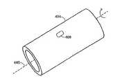
도 4a 내지 도 4c는 다른 실시예에서 집중 광 빔을 측정하기 위한 디바이스의 개략적인 측면도, 단부도 및 균등 투사도(isometric-projection view)이다;4A-4C are schematic side views, end views, and isometric-projection views of a device for measuring a concentrated light beam in another embodiment;
도 5a 내지 도 5b는 여전히 다른 실시예에서 집중 광 빔을 측정하기 위한 디바이스의 개략적인 측면도 및 균등 투사도이다; 그리고5A-5B are schematic side and even projection views of a device for measuring a focused light beam in still another embodiment; And
도 6은 추가의 실시예에서 집중 광 빔을 측정하기 위한 디바이스의 상부도이다.6 is a top view of the device for measuring the focused light beam in a further embodiment.
본 발명의 실시예들은 집중 광 빔에 의해 제공된 에너지 흐름에 응답하여 형광 발광하는 재료를 사용한다. 본 발명은 Thermal Flux Processing 애플리케이션에서 상세히 개시된 것과 같은 열 처리 시스템상의 동작 동안 발명자에 의해 개발되었으나, 본 발명은 이러한 애플리케이션들로 한정되지 않으며, 마찬가지의 다른 애플리케이션에 사용되는 집중 광 빔들을 프로파일링하는데 더욱 일반적으로 사용될 수 있다. Thermal Flux Processing 애플리케이션에 개시된 열 처리 시스템에 있어서, 집중 광 빔은 지속파 발광 소스에 의해 제공되며, 반도체-디바이스 제조업자를 위한 공정의 일부로서 기판 표면에 걸쳐 연장하는 발광 라인에 광학 장치에 의해 시준되고 집속된다. 집중 광에 의해 타겟의 표면에 발생된 열은 확산을 방지하기에 충분히 짧은 시간 프레임에서 어닐링에 유용한 높은 값으로 온도를 상승시킨다. 본 발명의 실시예들이 Thermal Flux Processing 애플리케이션에 개시된 것과 동일한 지속파 광 소스들과 함께 사용하기에 적합한 반면, 다른 실시예들은 버스트(burst)들, 펄스(pulse)들 또는 플래시(flash)들로서 제공되는 집중 광을 프로 파일링하기 위하여 사용될 수 있다. 또한, Thermal Flux Processing 애플리케이션에 개시된 광학 장치는 라인으로 광을 집속시키기 위하여 사용되는 반면, 본 발명의 상이한 실시예는 집중 광의 다른 기하학적 구성을 프로파일링하기 위하여 사용될 수 있다.Embodiments of the present invention use a material that fluoresces in response to the energy flow provided by the focused light beam. Although the present invention was developed by the inventor during operation on a thermal processing system such as that described in detail in Thermal Flux Processing applications, the present invention is not limited to these applications, and is more suitable for profiling concentrated light beams used in other applications as well. Generally can be used. In the thermal processing system disclosed in the Thermal Flux Processing application, the focused light beam is provided by a continuous wave light emitting source and is collimated by an optical device on a light emitting line extending across the substrate surface as part of a process for semiconductor-device manufacturers. Focused The heat generated on the surface of the target by the concentrated light raises the temperature to a high value useful for annealing in a time frame short enough to prevent diffusion. While embodiments of the invention are suitable for use with the same continuous wave light sources as disclosed in the Thermal Flux Processing application, other embodiments are provided as bursts, pulses or flashes. Can be used to profile the focused light. In addition, the optical devices disclosed in the Thermal Flux Processing application are used to focus light into lines, while different embodiments of the present invention can be used to profile other geometrical configurations of concentrated light.
다수의 실시예들에서, 집중 광 빔은 실질적으로 단색이다. 실리콘 기판이 사용되는 Thermal Flux Processing 애플리케이션에 개시된 특정 애플리케이션에 있어서, 집중 광은 약 190nm 내지 950nm 사이의 파장을 가지며, 808nm의 파장을 갖는 광의 특정 실시예가 개시된다. 하기 논의 중 일부에 있어서, 이러한 실시예는 또한 설명을 목적으로 논의되는 것이며, 본 발명은 집중 광 빔을 위한 임의의 특정 파장으로 제한되지 않는다. 또한, 본 발명은 단색 광 빔의 프로파일링으로 제한되지 않으며, 실시예들은 안정적인 스펙트럼들을 갖는 다른 빔들에 적용될 수 있다.In many embodiments, the focused light beam is substantially monochromatic. For certain applications disclosed in Thermal Flux Processing applications in which silicon substrates are used, specific embodiments of light having a wavelength between about 190 nm and 950 nm and having a wavelength of 808 nm are disclosed. In some of the following discussions, these embodiments are also discussed for purposes of illustration, and the present invention is not limited to any particular wavelength for the focused light beam. In addition, the present invention is not limited to the profiling of monochromatic light beams, and embodiments can be applied to other beams having stable spectra.
형광 물질과 집중된 광 빔의 상호작용에 의해 생성된 형광은 일반적으로는 집중된 광 빔과 동일한 프로파일 강도를 갖지만, 전체 강도는 현저히 감소되며 일반적으로 상이한 파장을 갖는다. 예를 들어, 몇몇 실시예들에서, 형광 물질은 1064nm의 파장에서 형광 발광함으로써 808nm 광 빔에 응답하는 네오디뮴:(이트륨 알루미늄 가넷)("Nd:YAG")을 포함한다. 광학 장치는 야기되는 808nm 및 1064nm 광의 조합을 분리하기 위하여 사용되어, 고강도의 808nm 광이 분실되도록 하고, 저강도의 1064nm 광을 센서로 지향시킨다. 저강도 1064nm 광은 감지기로부터 획득된 결과로 프로파일링되며, 고강도 808nm 광의 프로파일의 지표로서 사용된다. 상기 프로파일링은 저강도의 광으로 수행되기 때문에, 그것이 녹거나, 증발되거나, 또는 다른 방식으로 광의 강도에 의해 손상되는 점까지 적절한 측정 센서를 가열하는 하찮은 위험성이 존재한다.The fluorescence produced by the interaction of the fluorescent material with the focused light beam generally has the same profile intensity as the focused light beam, but the overall intensity is significantly reduced and generally has a different wavelength. For example, in some embodiments, the fluorescent material includes neodymium: (yttrium aluminum garnet) (“Nd: YAG”) responsive to the 808 nm light beam by fluorescing at a wavelength of 1064 nm. Optical devices are used to separate the resulting combination of 808nm and 1064nm light, causing high intensity 808nm light to be lost and directing low intensity 1064nm light to the sensor. Low intensity 1064 nm light is profiled with the results obtained from the detector and used as an indicator of the profile of high intensity 808 nm light. Since the profiling is performed with low intensity light, there is a minor risk of heating the appropriate measuring sensor to the point where it melts, evaporates, or otherwise is damaged by the intensity of the light.
도 1은 본 발명의 상이한 실시예들의 일반화된 개요를 제공한다. 블럭(104)에서, 파장(λ)을 포함하는 집중 광 빔은 프로파일링 디바이스로 지향된다. 광 빔은 블럭(108)에서 상이한 파장(λ')에서 형광 소스로부터 2차 광을 형광 발광시키기 위하여 사용된다. 파장(λ, λ')에서 조합된 광은 상기 광을 그것의 개별적인 파장 컴포넌트들로 분리하기 위하여 블럭(112)에서 스펙트럼 분리기로 지향된다. 프로파일링 디바이스의 광학 구조는 블럭(116)에서 나타나는 바와 같이, 파장(λ)에서 광이 손실되도록 하고, 측정을 위하여 파장(λ')에서 광이 센서로 지향되도록 한다.1 provides a generalized overview of different embodiments of the present invention. At
프로파일링 디바이스를 위한 특정한 하나의 실시예가 도 2에 개략적으로 도시된다. 프로파일링 디바이스는 유리와 같은, 파장(λ 및 λ')에서 일반적으로 광에 대하여 투명한 재료의 블럭(204)을 포함한다. 블럭(204)은 두 개의 파장들 중 하나에서 실질적으로 반사적이며, 두 개의 파장들 중 다른 하나의 파장에서 실질적으로 투과성(transmissive) 중간 표면(208)을 포함할 수 있다. 예를 들어, 광학 블럭(204)은 상기 표면들 중 하나가 원하는 투과/반사 특성을 갖는 광학 코팅으로 코팅된 후, 그들 각각의 빗변을 따라 결합되는 직각 프리즘의 반쪽들(halves)을 포함할 수 있다. 특정 예증에 있어서, 광학 코팅은, 프로파일링 디바이스상에 입사하는 광 빔(228)의 파장인 파장(λ)에서 투과성이며, 형광 소스(224)에 의해 생성된 2차 광의 파장인 파장(λ')에서 반사적이다. 도 2의 실시예에서, 라인 구조, 복수의 분리된 도트형 구조, 라인 구조와 도트형 구조의 결합, 또는 다른 기하학적 패턴들을 포함하는 다양한 상이한 기하학적 패턴들이 대안적인 실시예들에서 사용될 수 있으나, 형광 소스(224)는 도트형(dot-like) 구조로 제공된다. 형광 소스(224)는 입사 광 빔(228)이 2차 광을 생성하기 위하여 형광 소스(224)와 충돌하도록 몸체(204)의 표면에 가깝게 배치된다. 형광 소스(224)는 몸체(204)의 표면상에 배치될 수 있고, 또는 몸체의 표면 아래에 주입될 수 있다.One particular embodiment for a profiling device is shown schematically in FIG. 2. The profiling device includes a
2차 광(236)은 광학 장치의 다른 부분에 의해 센서(220)로 집속된다. 도 2에 도시된 특정 실시예는 광을 집속시키기 위하여 렌즈들(216)을 사용하나, 상기 집속을 달성하기 위하여 렌즈들의 임의의 장치 및/또는 거울과 같은 반사면들도 사용될 수 있다. 몇몇 실시예들에서, 윈스턴 콘(Winston cone)과 같은 입사되는 광선(incoming ray)들의 콜렉션을 증가시키도록 설계된 광학 컴포넌트가 사용될 수 있다. 광학 장치는 또한 초기 빔(228)로부터의 빗나간 광이 센서(220)로 지향되도록 하기 위하여 파장(λ')에서 투과성이나 2차 광(236)의 통로를 따라 파장(λ)에서 불투명한 필터(212)를 포함하는 것이 바람직하다. 렌즈(216)와 충돌하기에 앞서, 필터(212)는 2차 광(236)과 충돌하도록 배치되는 것으로 도시되는 반면, 충돌의 순서는 반대로 되고, 2차 광(236)은 그것이 필터(212)와 충돌하기 전에 렌즈들과 충돌한다. 센서(220)는 본 발명이 속하는 기술 분야의 공지된 형태의 광검출기를 포함할 수 있다. 동시에 프리즘 블럭(204), 렌즈들(216), 필터(212) 및 센서(220)를 이동시키는 것과 같이, 광학 장치의 빔을 이동시킴으로써, 센서(220)의 출력은 입사 빔(228)의 광 강도 프로파일을 나타낸다.The
대안적인 실시예가 도 3에 도시되며, 이는 또한 파장들(λ 및 λ')에서 실질적으로 빛나는 재료의 블럭(304)을 사용하고, 상기 파장들 중 하나에 실질적으로 반사적이며 상기 파장들 중 다른 하나에 실질적으로 투과성인 중간 표면(308)을 포함한다. 형광 물질의 다른 기하학적 패턴들 또는 불연속적 소스들을 제공하는 대신, 블럭(304)은 형광 물질의 막(320)으로 코팅되거나, 또는 형광 물질이 주입된다. 프로파일링 디바이스는 도 2와 관련하여 제공되는 기재와 유사한 다른 기능을 하며, 입사 광 빔(324)은 2차 광(332)을 생성하기 위하여 형광 물질의 막(320)과 상호작용한다. 파장(λ)에서의 최초 광 및 파장(λ')에서의 2차 광은 중간 표면(308)과 상호작용함으로써 상이한 방향으로 지향된다. 도 3은 파장(λ')이 반사되고 파장(λ)이 투과되는 특정한 경우를 도시하나, 전과 같이, 파장이 반사되고, 파장이 투과되는 것에는 아무런 문제가 없다. 2차 광은 이미지화(imaging)를 위하여 센서로 지향된다.An alternative embodiment is shown in FIG. 3, which also uses a
도 3은 또한 블럭(304)의 표면상에 이미지화된 광을 검출할 수 있는 카메라(316)로서 제공될 수 있는, 센서의 형태에 있어서의 또 다른 변형을 도시한다. 이러한 방식으로, 완전한 입사 빔(324)은 빔(324) 또는 광학 장치를 이동시키지 않으면서 프로파일링될 수 있다. 파장(λ')에서 광을 전송하나 파장(λ')에서 실질적으로 불투명한 필터(312)는 파장(λ)에서 빗나간 광이 카메라(316)에 도달하는 것을 방지하기 위항 2차 광의 통로를 따라 배치되는 것이 바람직할 수 있다. 카메라(316)는 상이한 실시예들에서 다른 형태의 카메라 또는 전하-결합(charge-coupled) 디바이스일 수 있다.3 also shows another variation in the shape of the sensor, which may be provided as a
전체 입사 빔을 프로파일링하기 위해 사용되는 움직임을 달성하기 위한 대안적인 장치들이 도 4a 내지 도 5b에 도시되며, 도 4a 내지 도 4c는 일 실시예를 도시하고, 도 5a 및 도 5b는 대안적인 실시예를 도시한다. 이러한 각각의 실시예들에 있어서, 동일한 일반적 구조는 2차 광을 검출기에 집속시키는 광학 장치의 일부분을 위하여 도시된다. 구조는 파장(λ')의 광을 전송하나 파장(λ)의 광은 전송하지 않는 필터 및 집속 렌즈를 포함하는 것으로 도시되나, 광선의 콜렉션을 증가시키기 위하여 윈스턴 콘과 같은 부가적 또는 대안적 광학 컴포넌트들을 포함할 수 있다.Alternative arrangements for achieving the motion used to profile the entire incident beam are shown in FIGS. 4A-5B, FIGS. 4A-4C show one embodiment, and FIGS. 5A-5B show an alternative implementation. An example is shown. In each of these embodiments, the same general structure is shown for the portion of the optical device that focuses secondary light to the detector. The structure is shown to include a filter and focusing lens that transmits light at wavelength λ 'but does not transmit light at wavelength λ', but additional or alternative optics, such as a Winston cone, to increase the collection of light rays. It may include components.
도 4a 내지 도 4c에 개시되는 실시예는 도 4a의 측면도, 도 4b의 단부도 및 도 4c의 균등 투사도와 함께 도시된다. 이러한 실시예는 파장들(λ 및 λ')에서 투명한 실린더(404)를 사용하고, 광학 장치의 적어도 일부분이 상기 투명한 실린더(404)내에 배치된다. 실린더(404)내에 배치된 광학 장치의 일부분을 배치하는 것은 실린더(404)가 중공 실린더로서 제공될 때 단순화되어, 광학 컴포넌트들이 상기 중공 부분내에 배치될 수 있다. 실린더(404)는 실린더가 축(440) 주변을 회전하도록 구성된 모터(미도시)와 결합된다. 이러한 회전은 실린더(404)의 표면상의 기하학적 패턴으로 배치된 형광 물질(408)이 상이한 위치로 이동하도록 하고, 회전 위치는 형광 물질의 위치와 동조화된다. 실린더(404)상에 투사하는 파장(λ)에서 광 빔(428)은 형광 물질이 파장(λ')에서 2차 광(436)을 방출하도록 한다. 조합된 광은 2차 광을 센서(420)로 지향시키는 광학 컴포넌트(424)와 분리되고, 렌즈(416)로 집속되며, 다른 실시예들과 관련하여 상기 개시된 바와 같이 필터(412)에 의해 필 터링된다. 조합된 광의 분리는 상기 개시된 것과 유사한 구조를 사용함으로써 달성될 수 있다. 특히, 광학 컴포넌트(424)는 파장(λ)에서 투과성이며, 파장(λ')에서 광을 반사하고 파장(λ)에서 광을 투과하는 코팅에 의해 커버되는 재료의 블럭을 포함할 수 있다. 대안적인 실시예들에서, 반사 및 전송 특성은 파장(λ')에서 2차 광이 투과되고, 그 후, 광을 집속시키고 감지하는 광학 장치의 일부분으로 지향되도록 역전될 수 있다.The embodiments disclosed in FIGS. 4A-4C are shown with the side view of FIG. 4A, the end view of FIG. 4B, and the even projection of FIG. 4C. This embodiment uses a
또 다른 변형이 도 5a 및 도 5b에 개시되며, 도 5a 및 5b는 각각 회전 디스크(504)를 사용하는 실시예의 측면도 및 균등 투사도를 제공한다. 디스크(504)는 파장(λ 및 λ')에서 광에 투명한 재료로 형성되며, 상기 개시된 것들과 유사한 기하학적 패턴으로 디스크(504) 표면상에 배치된 형광 물질(508)을 포함한다. 광학 장치는 도 4a 내지 도 4c와 관련하여 개시된 것과 유사하고, 광학 컴포넌트(512)는 파장들(λ 및 λ') 중 하나의 광을 반사하고 나머지 다른 하나의 파장의 광을 투과하도록 제공된다. 디스크(504)상을 투과하는 광 빔(528)은, 가능하다면, 빗나간 광이 센서(524)에 도달하는 것을 방지하기 위하여 필터에 의해 필터링된 후에, 형광 물질이 렌즈(520)를 사용하여 센서(524)상에 집속되는 2차 광(536)을 생성하도록 한다. 디스크(404) 및 광학 장치는 축(540) 주변의 회전을 야기하는 모터(미도시)와 결합되어, 입사 빔(528)의 상이한 부분들이 센서(524)에 의해 연속적으로 이미지화될 수 있다.Another variant is disclosed in FIGS. 5A and 5B, which provide side and even projection views of embodiments using
또 다른 대안이 도 6과 함께 개시되며, 도 6은 회전 디스크(604)를 사용하는 또 다른 실시예의 상부도를 제공한다. 형광 물질의 복수의 도트들(612)은 나선형 패턴으로 디스크 주변으로 분포되어 디스크(604)는 축(616) 주변을 회전하고, 도트들(612) 중 상이한 것들이 축(616)으로부터의 상이한 방사상 거리에서 빔(608)에 노출된다. 몇몇 실시예들에서, 디스크(604)는 신속하게 회전하여, 각각의 도트들(612)은 반복적으로, 그러나 상대적으로 짧은 시간 주기 동안 빔(608)에 노출된다. 그러한 실시예에서, 단일 검출기는 2차 광을 수집하기 위하여 사용될 수 있으며, 픽셀들 사이의 혼선(cross talk)은 최소화될 수 있다. 신속한 급회전(spinning)을 초래하는 부가적인 장점은 빔으로부터 흡수된 임의의 열이 상대적으로 큰 체적상에 분포되는 것이고, 이는 도트들의 듀티 사이클에 관련되며, 따라서, 최대 사용가능 전력 밀도를 증가시킨다. 설명을 목적으로, 본 발명자는 12cm의 직경을 갖는 디스크가 느린 축(slow axis)에서 약 4㎛ 해상도로 산출되고, 빠른 축(fast axis)에서 도트 크기가 제한될 수 있는 것으로 계산한다.Another alternative is disclosed in conjunction with FIG. 6, which provides a top view of another embodiment using a
상기 개시된 특정 실시예들은 본 발명의 상이한 측면들을 도시하기 위해 의도된 것이며, 특히, 조합된 λ 및 λ' 광을 분리하는데, 그리고 2차 광을 센서로 지향시키는데 다수의 대안들이 사용될 수 있다. 예를 들어, 광의 분리가 상기 파장들 중 하나에서 광을 투과하고 상기 파장들 중 다른 하나에서 광을 반사하는 코팅을 사용하는 각각의 실시예들에 개시된다. 그러한 구조는 특히, 광학 장치가 윈스턴 콘과 같은 광 수집을 개선하도록 설계된 컴포넌트를 더 포함할 때, 실질적으로 2차 광의 전체 강도가 계속 유지되고, 센서로 지향된다는 장점을 갖는다. 그러나, 다른 실시예들에서, 그러한 기술들이 2차 광의 강도에 있어서 얼마간의 손실을 초래한다 할지라도, 실질적으로 2색성의 광을 분리하기 위한 다른 기술이 사용될 수 있다. 예를 들어, 2색성 광이 초기에 집속되고, 분리기로 지향되는 장치는 2차 광을 수집하기 위하여 사용될 수 있으며, 분리기의 출력은 또한 파장(λ')의 광만을 통과시키는 필터로 지향된다. 이러한 장치 그리고 다른 유사한 장치들은 도 2 내지 도 6과 관련되어 다르게 개시된 구조와 조합될 수 있다.The specific embodiments disclosed above are intended to illustrate different aspects of the invention, and in particular, a number of alternatives may be used to separate the combined λ and λ ′ light and direct the secondary light to the sensor. For example, separation of light is disclosed in each of the embodiments using a coating that transmits light at one of the wavelengths and reflects light at the other of the wavelengths. Such a structure has the advantage that substantially when the optical device further comprises a component designed to improve light collection, such as a Winston cone, substantially the overall intensity of the secondary light is maintained and directed to the sensor. However, in other embodiments, even if such techniques result in some loss in the intensity of the secondary light, other techniques for substantially separating the dichroic light may be used. For example, dichroic light is initially focused and a device directed to the separator can be used to collect secondary light, and the output of the separator is also directed to a filter that only passes light of wavelength lambda '. Such devices and other similar devices may be combined with the structures disclosed differently with respect to FIGS.
또한, 대안적인 실시예들에서, 형광 물질의 사용은 입사 빔의 파장(λ)에서 광을 분산시키는데 작용하는 분산 특징을 제공함으로써 방지될 수 있고, 따라서, 그것의 강도를 현저하게 감소시켜 센서에 의해 샘플링될 수 있다. 그러한 분산 특징은 상기 개시된 투명한 구조들(204, 304, 404, 504)의 표면상에 배치될 수 있고, 또는 상기 투명한 구조들과 함께 내장될 수 있다. 광의 검출은 그 후, 입사 광의 파장(λ)에서 전송을 차단하는 필터를 포함하지 않고서 실행될 수 있다.Further, in alternative embodiments, the use of fluorescent material can be prevented by providing a scattering feature that acts to disperse light at the wavelength [lambda] of the incident beam, thus significantly reducing its intensity to the sensor. Can be sampled. Such dispersal feature may be disposed on the surface of the disclosed
개시된 다수의 실시예들을 가지고, 또 다른 변형, 대안적인 구성 및 그 동등물들이 본 발명의 정신을 벗어나지 않는 범위에서 사용될 수 있음이 본 발명이 속하는 분야의 당업자들에 의해 인지될 것이다. 따라서, 상기 개시는 다음의 청구항들에서 한정되는 본 발명의 범위를 제한하는 것으로 받아들여져서는 안될 것이다.It will be appreciated by those skilled in the art to which the present invention pertains that with a number of embodiments disclosed, that other variations, alternative configurations, and equivalents thereof may be used without departing from the spirit of the invention. Accordingly, the above disclosure should not be taken as limiting the scope of the invention as defined in the following claims.
Claims (25)
Translated fromKoreanApplications Claiming Priority (2)
| Application Number | Priority Date | Filing Date | Title |
|---|---|---|---|
| US62372004P | 2004-10-28 | 2004-10-28 | |
| US60/623,720 | 2004-10-28 |
Publications (1)
| Publication Number | Publication Date |
|---|---|
| KR20070065908Atrue KR20070065908A (en) | 2007-06-25 |
Family
ID=35840443
Family Applications (1)
| Application Number | Title | Priority Date | Filing Date |
|---|---|---|---|
| KR1020077010712ACeasedKR20070065908A (en) | 2004-10-28 | 2005-10-28 | Method and device for measuring concentrated light beam |
Country Status (6)
| Country | Link |
|---|---|
| US (2) | US7440088B2 (en) |
| EP (1) | EP1805490A1 (en) |
| JP (1) | JP4777995B2 (en) |
| KR (1) | KR20070065908A (en) |
| CN (1) | CN101048647A (en) |
| WO (1) | WO2006052512A1 (en) |
Families Citing this family (7)
| Publication number | Priority date | Publication date | Assignee | Title |
|---|---|---|---|---|
| US7947584B2 (en)* | 2008-05-02 | 2011-05-24 | Applied Materials, Inc. | Suitably short wavelength light for laser annealing of silicon in DSA type systems |
| US9018108B2 (en) | 2013-01-25 | 2015-04-28 | Applied Materials, Inc. | Low shrinkage dielectric films |
| DE102015016240B3 (en)* | 2015-12-16 | 2017-05-24 | Primes GmbH Meßtechnik für die Produktion mit Laserstrahlung | Transparent measuring probe for beam scanning |
| DE102016011568B4 (en) | 2016-09-26 | 2019-03-07 | Primes GmbH Meßtechnik für die Produktion mit Laserstrahlung | Apparatus and method for determining spatial dimensions of a light beam |
| JP6244502B1 (en)* | 2017-04-17 | 2017-12-06 | カナレ電気株式会社 | Laser beam profile measuring device |
| US11067438B2 (en) | 2017-07-27 | 2021-07-20 | Canare Electric Co., Ltd. | Laser beam profile measurement device |
| JPWO2020179049A1 (en)* | 2019-03-07 | 2021-11-25 | カナレ電気株式会社 | Laser beam profile measuring device |
Family Cites Families (19)
| Publication number | Priority date | Publication date | Assignee | Title |
|---|---|---|---|---|
| US4425907A (en)* | 1980-09-25 | 1984-01-17 | Exxon Research And Engineering Co. | Reflector-coupled fluorescent solar collector |
| DE3706271A1 (en)* | 1987-02-26 | 1988-09-08 | Erwin Strigl | DEVICE FOR MEASURING THE INTENSITY PROFILE OF A LASER BEAM |
| DE3738480A1 (en)* | 1987-11-12 | 1989-05-24 | Lambda Physik Forschung | Method and device for measuring the intensity of a UV-laser beam |
| US4885471A (en)* | 1988-04-22 | 1989-12-05 | Taunton Technologies, Inc. | Ultraviolet radiometer |
| JPH05231929A (en)* | 1992-02-25 | 1993-09-07 | Chiyoda Kohan Kk | Measuring apparatus of illuminance of ultraviolet ray |
| IL106747A0 (en)* | 1993-08-20 | 1993-12-08 | Oren Aharon | Laser beam analyzer |
| JP3529195B2 (en)* | 1994-06-21 | 2004-05-24 | 株式会社住田光学ガラス | Infrared visible wavelength up-conversion material |
| JP3469337B2 (en)* | 1994-12-16 | 2003-11-25 | 株式会社半導体エネルギー研究所 | Method for manufacturing semiconductor device |
| JPH08304172A (en)* | 1995-04-28 | 1996-11-22 | Advantest Corp | Polarization-independent optical detector |
| WO1999020428A1 (en)* | 1997-10-22 | 1999-04-29 | Fraunhofer-Gesellschaft zur Förderung der angewandten Forschung e.V. | Method and device for treating work pieces with laser radiation |
| US5922617A (en)* | 1997-11-12 | 1999-07-13 | Functional Genetics, Inc. | Rapid screening assay methods and devices |
| US6114704A (en)* | 1998-10-13 | 2000-09-05 | Cymer, Inc. | Front-illuminated fluorescent screen for UV imaging |
| US6393042B1 (en)* | 1999-03-08 | 2002-05-21 | Semiconductor Energy Laboratory Co., Ltd. | Beam homogenizer and laser irradiation apparatus |
| US6531681B1 (en)* | 2000-03-27 | 2003-03-11 | Ultratech Stepper, Inc. | Apparatus having line source of radiant energy for exposing a substrate |
| JP2003031467A (en)* | 2001-07-13 | 2003-01-31 | Canon Inc | Projection exposure apparatus, projection exposure method, and semiconductor manufacturing method |
| JP2003042844A (en)* | 2001-07-31 | 2003-02-13 | Konica Corp | Apparatus and method for measurement of ultraviolet quantity |
| GB0201916D0 (en) | 2002-01-29 | 2002-03-13 | Advanced Laser Solutions Ltd | Method and apparatus for monitoring light beams |
| US6987240B2 (en) | 2002-04-18 | 2006-01-17 | Applied Materials, Inc. | Thermal flux processing by scanning |
| US7341880B2 (en)* | 2003-09-17 | 2008-03-11 | Luminus Devices, Inc. | Light emitting device processes |
- 2005
- 2005-10-28EPEP05824935Apatent/EP1805490A1/ennot_activeWithdrawn
- 2005-10-28JPJP2007539259Apatent/JP4777995B2/ennot_activeExpired - Fee Related
- 2005-10-28CNCNA2005800373171Apatent/CN101048647A/enactivePending
- 2005-10-28KRKR1020077010712Apatent/KR20070065908A/ennot_activeCeased
- 2005-10-28USUS11/261,439patent/US7440088B2/ennot_activeExpired - Fee Related
- 2005-10-28WOPCT/US2005/039308patent/WO2006052512A1/enactiveApplication Filing
- 2008
- 2008-08-29USUS12/201,251patent/US20090015830A1/ennot_activeAbandoned
Also Published As
| Publication number | Publication date |
|---|---|
| US20060158641A1 (en) | 2006-07-20 |
| CN101048647A (en) | 2007-10-03 |
| EP1805490A1 (en) | 2007-07-11 |
| US20090015830A1 (en) | 2009-01-15 |
| JP4777995B2 (en) | 2011-09-21 |
| WO2006052512A1 (en) | 2006-05-18 |
| US7440088B2 (en) | 2008-10-21 |
| JP2008519263A (en) | 2008-06-05 |
Similar Documents
| Publication | Publication Date | Title |
|---|---|---|
| Veron et al. | Optical spatial smoothing of Nd-glass laser beam | |
| JP5103186B2 (en) | Multi-band pass filtering for high temperature measurements in laser-based annealing systems | |
| US9201016B2 (en) | Device for the contactless and nondestructive testing of surfaces | |
| US20090015830A1 (en) | Methods and devices for measuring a concentrated light beam | |
| JPH01170591A (en) | Work processing apparatus | |
| WO1997016387A1 (en) | Laser-based method of forming an image in transparent objects | |
| US20080142730A1 (en) | Fluorescence detecting device | |
| US7804042B2 (en) | Pryometer for laser annealing system compatible with amorphous carbon optical absorber layer | |
| JP2008520096A5 (en) | ||
| US11712754B2 (en) | Device and method for laser-based separation of a transparent, brittle workpiece | |
| JP6956328B2 (en) | Laser processing equipment and laser processing method | |
| JP2008122297A (en) | Fluorescence detection apparatus and fluorescence detection method | |
| US20060102599A1 (en) | Rapid detection of imminent failure in laser thermal processing of a substrate | |
| CN114114095A (en) | Magnetic Measurement System Based on Diamond NV Color Center | |
| JP2003215389A (en) | Optical fiber collimator and manufacturing method therefor | |
| US6734448B2 (en) | Method and apparatus for boresighting a laser with a forward looking infrared device | |
| JP2010101891A (en) | High intensity pulsed light source configuration | |
| JP6244502B1 (en) | Laser beam profile measuring device | |
| JP2580183B2 (en) | Radiation image reader | |
| CN209133830U (en) | A kind of laser pump (ing) fluorescent light source device | |
| JPH10303513A (en) | Semiconductor laser device | |
| JP2022061443A (en) | Laser device | |
| RU2001135117A (en) | METHOD FOR MEASURING DIFFUSINGLY REFLECTING SURFACE | |
| JPH0294487A (en) | Solid laser device |
Legal Events
| Date | Code | Title | Description |
|---|---|---|---|
| A201 | Request for examination | ||
| PA0105 | International application | Patent event date:20070511 Patent event code:PA01051R01D Comment text:International Patent Application | |
| PA0201 | Request for examination | ||
| PG1501 | Laying open of application | ||
| E902 | Notification of reason for refusal | ||
| PE0902 | Notice of grounds for rejection | Comment text:Notification of reason for refusal Patent event date:20080430 Patent event code:PE09021S01D | |
| E902 | Notification of reason for refusal | ||
| PE0902 | Notice of grounds for rejection | Comment text:Notification of reason for refusal Patent event date:20081216 Patent event code:PE09021S01D | |
| E902 | Notification of reason for refusal | ||
| PE0902 | Notice of grounds for rejection | Comment text:Notification of reason for refusal Patent event date:20090623 Patent event code:PE09021S01D | |
| E601 | Decision to refuse application | ||
| PE0601 | Decision on rejection of patent | Patent event date:20090925 Comment text:Decision to Refuse Application Patent event code:PE06012S01D Patent event date:20090623 Comment text:Notification of reason for refusal Patent event code:PE06011S01I Patent event date:20081216 Comment text:Notification of reason for refusal Patent event code:PE06011S01I Patent event date:20080430 Comment text:Notification of reason for refusal Patent event code:PE06011S01I |