KR20070054100A - Selective Etching Method of Titanium Nitride Using Xenon Difluoride - Google Patents
Selective Etching Method of Titanium Nitride Using Xenon DifluorideDownload PDFInfo
- Publication number
- KR20070054100A KR20070054100AKR1020060112517AKR20060112517AKR20070054100AKR 20070054100 AKR20070054100 AKR 20070054100AKR 1020060112517 AKR1020060112517 AKR 1020060112517AKR 20060112517 AKR20060112517 AKR 20060112517AKR 20070054100 AKR20070054100 AKR 20070054100A
- Authority
- KR
- South Korea
- Prior art keywords
- contacting
- xenon
- tin
- xenon difluoride
- xef
- Prior art date
- Legal status (The legal status is an assumption and is not a legal conclusion. Google has not performed a legal analysis and makes no representation as to the accuracy of the status listed.)
- Abandoned
Links
- 238000000034methodMethods0.000titleclaimsabstractdescription64
- 238000005530etchingMethods0.000titleclaimsabstractdescription26
- NRTOMJZYCJJWKI-UHFFFAOYSA-NTitanium nitrideChemical compound[Ti]#NNRTOMJZYCJJWKI-UHFFFAOYSA-N0.000titleclaimsdescription52
- BLIQUJLAJXRXSG-UHFFFAOYSA-N1-benzyl-3-(trifluoromethyl)pyrrolidin-1-ium-3-carboxylateChemical compoundC1C(C(=O)O)(C(F)(F)F)CCN1CC1=CC=CC=C1BLIQUJLAJXRXSG-UHFFFAOYSA-N0.000titleclaimsdescription13
- VYPSYNLAJGMNEJ-UHFFFAOYSA-NSilicium dioxideChemical compoundO=[Si]=OVYPSYNLAJGMNEJ-UHFFFAOYSA-N0.000claimsabstractdescription41
- 230000008021depositionEffects0.000claimsabstractdescription32
- 235000012239silicon dioxideNutrition0.000claimsabstractdescription25
- 239000000463materialSubstances0.000claimsabstractdescription19
- 150000002222fluorine compoundsChemical class0.000claimsabstractdescription16
- 239000004065semiconductorSubstances0.000claimsabstractdescription16
- 239000000377silicon dioxideSubstances0.000claimsabstractdescription15
- 238000011065in-situ storageMethods0.000claimsabstractdescription11
- 238000006243chemical reactionMethods0.000claimsabstractdescription7
- 239000003039volatile agentSubstances0.000claimsabstractdescription6
- 229910052581Si3N4Inorganic materials0.000claimsdescription36
- HQVNEWCFYHHQES-UHFFFAOYSA-Nsilicon nitrideChemical compoundN12[Si]34N5[Si]62N3[Si]51N64HQVNEWCFYHHQES-UHFFFAOYSA-N0.000claimsdescription36
- 239000007789gasSubstances0.000claimsdescription33
- XKRFYHLGVUSROY-UHFFFAOYSA-NArgonChemical compound[Ar]XKRFYHLGVUSROY-UHFFFAOYSA-N0.000claimsdescription10
- 238000004140cleaningMethods0.000claimsdescription10
- 229910052724xenonInorganic materials0.000claimsdescription8
- 229910052786argonInorganic materials0.000claimsdescription7
- FHNFHKCVQCLJFQ-UHFFFAOYSA-Nxenon atomChemical compound[Xe]FHNFHKCVQCLJFQ-UHFFFAOYSA-N0.000claimsdescription7
- 238000010952in-situ formationMethods0.000claimsdescription5
- 229910004298SiO 2Inorganic materials0.000abstractdescription41
- 239000010453quartzSubstances0.000abstractdescription10
- ATJFFYVFTNAWJD-UHFFFAOYSA-NTinChemical compound[Sn]ATJFFYVFTNAWJD-UHFFFAOYSA-N0.000abstract3
- 238000000151depositionMethods0.000description28
- 230000008569processEffects0.000description28
- 239000010408filmSubstances0.000description20
- 239000000758substrateSubstances0.000description18
- XUIMIQQOPSSXEZ-UHFFFAOYSA-NSiliconChemical compound[Si]XUIMIQQOPSSXEZ-UHFFFAOYSA-N0.000description8
- 229910052710siliconInorganic materials0.000description8
- 239000010703siliconSubstances0.000description8
- 125000001153fluoro groupChemical groupF*0.000description7
- 230000001965increasing effectEffects0.000description7
- RTAQQCXQSZGOHL-UHFFFAOYSA-NTitaniumChemical compound[Ti]RTAQQCXQSZGOHL-UHFFFAOYSA-N0.000description5
- 238000005229chemical vapour depositionMethods0.000description5
- 238000002474experimental methodMethods0.000description5
- 239000010936titaniumSubstances0.000description5
- 229910052719titaniumInorganic materials0.000description5
- YCKRFDGAMUMZLT-UHFFFAOYSA-NFluorine atomChemical compound[F]YCKRFDGAMUMZLT-UHFFFAOYSA-N0.000description4
- 238000005137deposition processMethods0.000description4
- 230000000694effectsEffects0.000description4
- 229910052731fluorineInorganic materials0.000description4
- 239000011737fluorineSubstances0.000description4
- 229910052721tungstenInorganic materials0.000description4
- 239000010937tungstenSubstances0.000description4
- 238000004519manufacturing processMethods0.000description3
- WFKWXMTUELFFGS-UHFFFAOYSA-NtungstenChemical compound[W]WFKWXMTUELFFGS-UHFFFAOYSA-N0.000description3
- ZOKXTWBITQBERF-UHFFFAOYSA-NMolybdenumChemical compound[Mo]ZOKXTWBITQBERF-UHFFFAOYSA-N0.000description2
- 230000015572biosynthetic processEffects0.000description2
- -1chlorine trifluoride Sulfur hexafluorideChemical compound0.000description2
- 230000007547defectEffects0.000description2
- 238000010894electron beam technologyMethods0.000description2
- 229910052734heliumInorganic materials0.000description2
- 230000006872improvementEffects0.000description2
- 239000011261inert gasSubstances0.000description2
- 239000000203mixtureSubstances0.000description2
- 229910052750molybdenumInorganic materials0.000description2
- 239000011733molybdenumSubstances0.000description2
- 238000000623plasma-assisted chemical vapour depositionMethods0.000description2
- 229910021420polycrystalline siliconInorganic materials0.000description2
- 239000003870refractory metalSubstances0.000description2
- 229910021332silicideInorganic materials0.000description2
- 239000010409thin filmSubstances0.000description2
- 235000012431wafersNutrition0.000description2
- 238000005406washingMethods0.000description2
- 229910000881Cu alloyInorganic materials0.000description1
- 238000009825accumulationMethods0.000description1
- 230000002411adverseEffects0.000description1
- WPPDFTBPZNZZRP-UHFFFAOYSA-Naluminum copperChemical compound[Al].[Cu]WPPDFTBPZNZZRP-UHFFFAOYSA-N0.000description1
- 230000008859changeEffects0.000description1
- 239000012459cleaning agentSubstances0.000description1
- 150000001875compoundsChemical class0.000description1
- 239000004020conductorSubstances0.000description1
- 239000000356contaminantSubstances0.000description1
- 230000007423decreaseEffects0.000description1
- 239000010432diamondSubstances0.000description1
- 229910003460diamondInorganic materials0.000description1
- 238000010494dissociation reactionMethods0.000description1
- 230000005593dissociationsEffects0.000description1
- 230000002708enhancing effectEffects0.000description1
- NBVXSUQYWXRMNV-UHFFFAOYSA-NfluoromethaneChemical compoundFCNBVXSUQYWXRMNV-UHFFFAOYSA-N0.000description1
- 230000002401inhibitory effectEffects0.000description1
- 238000010849ion bombardmentMethods0.000description1
- 150000002500ionsChemical class0.000description1
- 229910052743kryptonInorganic materials0.000description1
- QKCGXXHCELUCKW-UHFFFAOYSA-Nn-[4-[4-(dinaphthalen-2-ylamino)phenyl]phenyl]-n-naphthalen-2-ylnaphthalen-2-amineChemical compoundC1=CC=CC2=CC(N(C=3C=CC(=CC=3)C=3C=CC(=CC=3)N(C=3C=C4C=CC=CC4=CC=3)C=3C=C4C=CC=CC4=CC=3)C3=CC4=CC=CC=C4C=C3)=CC=C21QKCGXXHCELUCKW-UHFFFAOYSA-N0.000description1
- GVGCUCJTUSOZKP-UHFFFAOYSA-Nnitrogen trifluorideChemical compoundFN(F)FGVGCUCJTUSOZKP-UHFFFAOYSA-N0.000description1
- NJPPVKZQTLUDBO-UHFFFAOYSA-NnovaluronChemical compoundC1=C(Cl)C(OC(F)(F)C(OC(F)(F)F)F)=CC=C1NC(=O)NC(=O)C1=C(F)C=CC=C1FNJPPVKZQTLUDBO-UHFFFAOYSA-N0.000description1
- 239000002245particleSubstances0.000description1
- 239000013618particulate matterSubstances0.000description1
- 229920005591polysiliconPolymers0.000description1
- 239000000376reactantSubstances0.000description1
- 230000008439repair processEffects0.000description1
- HBMJWWWQQXIZIP-UHFFFAOYSA-Nsilicon carbideChemical compound[Si+]#[C-]HBMJWWWQQXIZIP-UHFFFAOYSA-N0.000description1
- 229910010271silicon carbideInorganic materials0.000description1
- LIVNPJMFVYWSIS-UHFFFAOYSA-Nsilicon monoxideChemical compound[Si-]#[O+]LIVNPJMFVYWSIS-UHFFFAOYSA-N0.000description1
- 229910052814silicon oxideInorganic materials0.000description1
- 239000007787solidSubstances0.000description1
- 238000009987spinningMethods0.000description1
- 239000000126substanceSubstances0.000description1
- 150000003463sulfurChemical class0.000description1
- MZLGASXMSKOWSE-UHFFFAOYSA-Ntantalum nitrideChemical compound[Ta]#NMZLGASXMSKOWSE-UHFFFAOYSA-N0.000description1
- TXEYQDLBPFQVAA-UHFFFAOYSA-NtetrafluoromethaneChemical compoundFC(F)(F)FTXEYQDLBPFQVAA-UHFFFAOYSA-N0.000description1
- 229910021341titanium silicideInorganic materials0.000description1
- WQJQOUPTWCFRMM-UHFFFAOYSA-Ntungsten disilicideChemical compound[Si]#[W]#[Si]WQJQOUPTWCFRMM-UHFFFAOYSA-N0.000description1
- 229910021342tungsten silicideInorganic materials0.000description1
- 238000011144upstream manufacturingMethods0.000description1
Images


Classifications
- C—CHEMISTRY; METALLURGY
- C23—COATING METALLIC MATERIAL; COATING MATERIAL WITH METALLIC MATERIAL; CHEMICAL SURFACE TREATMENT; DIFFUSION TREATMENT OF METALLIC MATERIAL; COATING BY VACUUM EVAPORATION, BY SPUTTERING, BY ION IMPLANTATION OR BY CHEMICAL VAPOUR DEPOSITION, IN GENERAL; INHIBITING CORROSION OF METALLIC MATERIAL OR INCRUSTATION IN GENERAL
- C23C—COATING METALLIC MATERIAL; COATING MATERIAL WITH METALLIC MATERIAL; SURFACE TREATMENT OF METALLIC MATERIAL BY DIFFUSION INTO THE SURFACE, BY CHEMICAL CONVERSION OR SUBSTITUTION; COATING BY VACUUM EVAPORATION, BY SPUTTERING, BY ION IMPLANTATION OR BY CHEMICAL VAPOUR DEPOSITION, IN GENERAL
- C23C16/00—Chemical coating by decomposition of gaseous compounds, without leaving reaction products of surface material in the coating, i.e. chemical vapour deposition [CVD] processes
- C23C16/44—Chemical coating by decomposition of gaseous compounds, without leaving reaction products of surface material in the coating, i.e. chemical vapour deposition [CVD] processes characterised by the method of coating
- C23C16/4401—Means for minimising impurities, e.g. dust, moisture or residual gas, in the reaction chamber
- C23C16/4405—Cleaning of reactor or parts inside the reactor by using reactive gases
- H—ELECTRICITY
- H01—ELECTRIC ELEMENTS
- H01L—SEMICONDUCTOR DEVICES NOT COVERED BY CLASS H10
- H01L21/00—Processes or apparatus adapted for the manufacture or treatment of semiconductor or solid state devices or of parts thereof
- H01L21/02—Manufacture or treatment of semiconductor devices or of parts thereof
- H01L21/04—Manufacture or treatment of semiconductor devices or of parts thereof the devices having potential barriers, e.g. a PN junction, depletion layer or carrier concentration layer
- H01L21/18—Manufacture or treatment of semiconductor devices or of parts thereof the devices having potential barriers, e.g. a PN junction, depletion layer or carrier concentration layer the devices having semiconductor bodies comprising elements of Group IV of the Periodic Table or AIIIBV compounds with or without impurities, e.g. doping materials
- H01L21/30—Treatment of semiconductor bodies using processes or apparatus not provided for in groups H01L21/20 - H01L21/26
- H01L21/302—Treatment of semiconductor bodies using processes or apparatus not provided for in groups H01L21/20 - H01L21/26 to change their surface-physical characteristics or shape, e.g. etching, polishing, cutting
- B—PERFORMING OPERATIONS; TRANSPORTING
- B08—CLEANING
- B08B—CLEANING IN GENERAL; PREVENTION OF FOULING IN GENERAL
- B08B7/00—Cleaning by methods not provided for in a single other subclass or a single group in this subclass
- B08B7/0035—Cleaning by methods not provided for in a single other subclass or a single group in this subclass by radiant energy, e.g. UV, laser, light beam or the like
- H—ELECTRICITY
- H01—ELECTRIC ELEMENTS
- H01L—SEMICONDUCTOR DEVICES NOT COVERED BY CLASS H10
- H01L21/00—Processes or apparatus adapted for the manufacture or treatment of semiconductor or solid state devices or of parts thereof
- H01L21/02—Manufacture or treatment of semiconductor devices or of parts thereof
- H01L21/04—Manufacture or treatment of semiconductor devices or of parts thereof the devices having potential barriers, e.g. a PN junction, depletion layer or carrier concentration layer
- H01L21/18—Manufacture or treatment of semiconductor devices or of parts thereof the devices having potential barriers, e.g. a PN junction, depletion layer or carrier concentration layer the devices having semiconductor bodies comprising elements of Group IV of the Periodic Table or AIIIBV compounds with or without impurities, e.g. doping materials
- H01L21/30—Treatment of semiconductor bodies using processes or apparatus not provided for in groups H01L21/20 - H01L21/26
- H01L21/31—Treatment of semiconductor bodies using processes or apparatus not provided for in groups H01L21/20 - H01L21/26 to form insulating layers thereon, e.g. for masking or by using photolithographic techniques; After treatment of these layers; Selection of materials for these layers
- H01L21/3205—Deposition of non-insulating-, e.g. conductive- or resistive-, layers on insulating layers; After-treatment of these layers
- H01L21/321—After treatment
- H01L21/3213—Physical or chemical etching of the layers, e.g. to produce a patterned layer from a pre-deposited extensive layer
- H01L21/32133—Physical or chemical etching of the layers, e.g. to produce a patterned layer from a pre-deposited extensive layer by chemical means only
- H01L21/32135—Physical or chemical etching of the layers, e.g. to produce a patterned layer from a pre-deposited extensive layer by chemical means only by vapour etching only
- H01L21/32136—Physical or chemical etching of the layers, e.g. to produce a patterned layer from a pre-deposited extensive layer by chemical means only by vapour etching only using plasmas
- H—ELECTRICITY
- H01—ELECTRIC ELEMENTS
- H01L—SEMICONDUCTOR DEVICES NOT COVERED BY CLASS H10
- H01L21/00—Processes or apparatus adapted for the manufacture or treatment of semiconductor or solid state devices or of parts thereof
- H01L21/67—Apparatus specially adapted for handling semiconductor or electric solid state devices during manufacture or treatment thereof; Apparatus specially adapted for handling wafers during manufacture or treatment of semiconductor or electric solid state devices or components ; Apparatus not specifically provided for elsewhere
- H01L21/67005—Apparatus not specifically provided for elsewhere
- H01L21/67011—Apparatus for manufacture or treatment
- H01L21/67017—Apparatus for fluid treatment
- H01L21/67028—Apparatus for fluid treatment for cleaning followed by drying, rinsing, stripping, blasting or the like
Landscapes
- Engineering & Computer Science (AREA)
- Chemical & Material Sciences (AREA)
- Physics & Mathematics (AREA)
- Condensed Matter Physics & Semiconductors (AREA)
- General Physics & Mathematics (AREA)
- Manufacturing & Machinery (AREA)
- Computer Hardware Design (AREA)
- Microelectronics & Electronic Packaging (AREA)
- Power Engineering (AREA)
- General Chemical & Material Sciences (AREA)
- Chemical Kinetics & Catalysis (AREA)
- Plasma & Fusion (AREA)
- Optics & Photonics (AREA)
- Materials Engineering (AREA)
- Mechanical Engineering (AREA)
- Metallurgy (AREA)
- Organic Chemistry (AREA)
- Drying Of Semiconductors (AREA)
- ing And Chemical Polishing (AREA)
Abstract
Translated fromKoreanDescription
Translated fromKorean도 1은 NF3 원격 플라스마에서 Ar에 대한 Xe 수치의 함수로 규소 기판의 에칭 속도의 플롯이다.1 is a plot of the etch rate of a silicon substrate as a function of Xe values for Ar in an NF3 remote plasma.
도 2는 NF3 원격 플라스마에서 Ar에 대한 Xe 수치의 함수로 SiO2의 에칭 속도의 플롯이다.FIG. 2 is a plot of the etch rate of SiO2 as a function of Xe values for Ar in NF3 remote plasma.
도 3은 NF3 원격 플라스마에서 Ar에 대한 Xe 수치의 함수로 규소의 이산화규소에 대한 에칭 선택성을 비교하는 플롯이다.FIG. 3 is a plot comparing silicon etch selectivity for silicon dioxide as a function of Xe values for Ar in NF3 remote plasma.
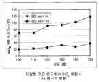
도 4는 NF3 원격 플라스마에서 Ar에 대한 Xe 수치 및 온도의 함수로 TiN의 에칭 속도의 플롯이다.4 is a plot of etch rate of TiN as a function of Xe values and temperature for Ar in NF3 remote plasma.
도 5는 NF3 원격 플라스마에서 Ar에 대한 Xe 수치 및 온도의 함수로 이산화규소의 에칭 속도의 플롯이다.5 is a plot of the etch rate of silicon dioxide as a function of Xe values and temperature for Ar in NF3 remote plasma.
도 6은 NF3 원격 플라스마에서 Ar에 대한 Xe 수치의 함수로 TiN의 이산화규소에 대한 에칭 선택성을 비교하는 플롯이다.FIG. 6 is a plot comparing TiN etch selectivity for silicon dioxide as a function of Xe values for Ar in NF3 remote plasma.
전자 산업 분야에서, 선택된 물질을 표적 기판상에 증착시켜 반도체와 같은 전자 부품을 제조하는 다양한 증착 기술이 개발되어 왔다. 증착 공정의 한 유형으로, 기체 반응물이 가열된 공정 챔버로 도입되어 소정의 기판상에 증착된 필름을 얻는 화학적 기상 증착(CVD)이 있다. CVD의 하나의 하위 유형으로는 플라스마를 CVD 공정 챔버에 가하는 플라스마 강화된 CVD(PECVD)를 언급할 수 있다.In the electronics industry, various deposition techniques have been developed for depositing selected materials onto target substrates to produce electronic components such as semiconductors. One type of deposition process is chemical vapor deposition (CVD), in which gaseous reactants are introduced into a heated process chamber to obtain a deposited film on a given substrate. One subtype of CVD may refer to plasma enhanced CVD (PECVD) that applies plasma to the CVD process chamber.
일반적으로, 모든 증착 방법은 표적 기판이 아닌 다른 표면상에 미립자 물질 및 필름의 축적을 초래하는데, 다시 말해, 증착 물질이 증착 공정에 사용된 벽, 도구 표면, 서스셉터(susceptor), 및 기타 장치상에도 모이게 된다. 벽, 도구 표면, 서스셉터, 및 기타 장치상에 축적된 임의의 물질, 필름 등은 오염물로 간주되어, 전자 제품 부품에 결함을 초래할 수 있다.In general, all deposition methods result in the accumulation of particulate matter and films on surfaces other than the target substrate, ie walls, tool surfaces, susceptors, and other devices in which the deposition material is used in the deposition process. You will also gather on the table. Any material, film, and the like accumulated on walls, tool surfaces, susceptors, and other devices can be considered contaminants, causing defects in electronic product components.
증착 챔버, 도구 및 장치는 불필요한 오염 증착 물질을 제거하기 위해 주기적으로 세척되어야 한다. 증착 챔버, 도구 및 장치를 세척하는 일반적으로 바람직한 방법에는, 과불소화된 화합물(PFC), 예를 들어, C2F6, CF4, C3F8, SF6 및 NF3를 에칭화 세척제로 사용하는 것이 포함된다. 이러한 세척 작업에서, 공정 기체로 주로 사용되는 화학적으로 활성있는 불소 물질은 불필요하고 오염된 잔여물을 휘발성 생성물로 전환시킨다. 그 후, 휘발성 생성물은 반응기로부터 공정 기체와 함께 쓸려나간다.Deposition chambers, tools and devices should be cleaned periodically to remove unnecessary contaminated deposition material. Generally preferred methods for cleaning deposition chambers, tools and devices include perfluorinated compounds (PFCs), such as C2 F6 , CF4 , C3 F8 , SF6 and NF3 , with etched cleaning agents. Use is included. In this cleaning operation, chemically active fluorine substances, which are mainly used as process gases, convert unwanted and contaminated residues into volatile products. The volatile product is then swept away from the reactor with the process gas.
이하 참고문헌은 반도체 제작시의 필름 증착 공정, 및 증착 챔버, 도구 및 장치의 세척 방법, 및 기판의 에칭 방법을 설명한다:The following references describe film deposition processes in semiconductor fabrication, and methods of cleaning deposition chambers, tools and devices, and methods of etching substrates:
US 5,421,957은 차가운 벽의 CVD-챔버의 저온 세척 방법을 공개한다. 이 방법은 수분이 없는 조건하에서 인시투로 수행된다. 에피택시얼 규소, 폴리규소, 질화규소, 산화규소 및 난융금속, 티타늄, 텅스텐, 및 이들의 규화물과 같은 다양한 물질로 된 필름의 세척에, 에칭화 기체, 예를 들어, 삼불화질소, 삼불화염소, 육불화황 및 사불화탄소를 사용한다.US 5,421,957 discloses a cold cleaning method of a cold wall CVD-chamber. This method is carried out in situ under water-free conditions. For the cleaning of films of various materials such as epitaxial silicon, polysilicon, silicon nitride, silicon oxide and refractory metals, titanium, tungsten, and silicides thereof, etching gases such as nitrogen trifluoride, chlorine trifluoride Sulfur hexafluoride and carbon tetrafluoride are used.
US 6,051,052는 이온 강화된 플라스마에서 에칭제로 불소 화합물, 예를 들어, NF3 및 C2F6을 사용하여 전도체 물질을 이방성 에칭하는 방법에 대해 공개한다. 에칭제는 불소 화합물과, He, Ar, Xe 및 Kr로 구성된 군에서 선택된 희가스로 구성된다. 테스트되는 기판에는 기판과 결합된 집적 회로가 포함된다. 한 구체예에서, 티타늄층이 절연층 위에 형성되며, 이는 텅스텐 플러그와 접촉해 있다. 이후, 알루미늄-구리 합금층이 티타늄층 위에 형성되며, 질화티타늄층이 그 위에 형성된다.US 6,051,052 discloses a method for anisotropically etching conductor materials using fluorine compounds such as NF3 and C2 F6 as etchant in ion enhanced plasma. The etchant consists of a fluorine compound and a rare gas selected from the group consisting of He, Ar, Xe and Kr. The substrate tested includes an integrated circuit coupled with the substrate. In one embodiment, a titanium layer is formed over the insulating layer, which is in contact with the tungsten plug. Then, an aluminum-copper alloy layer is formed on the titanium layer, and a titanium nitride layer is formed thereon.
US 2003/0047691은 리소그래피 마스크에서 전자 빔을 사용하여 물질을 에칭 또는 증착시키거나 결함을 복원하는 것에 대해 공개한다. 한 구체예에서, 이불화크세논은 전자 빔에 의해 활성화되어, 질화텅스텐 및 질화탄탈을 에칭한다.US 2003/0047691 discloses the use of an electron beam in a lithographic mask to etch or deposit material or to repair defects. In one embodiment, xenon difluoride is activated by an electron beam to etch tungsten nitride and tantalum nitride.
GB 2,183,204 A는 CVD 증착 하드웨어, 보트, 튜브, 및 석영 웨어는 물론, 반도체 웨이퍼의 인시투 세척에 NF3를 사용하는 것에 대해 공개하고 있다. NF3는 350℃를 초과하는 온도에서 질화규소, 다중결정질 규소, 규화티타늄, 규화텅스텐, 난 융금속 및 규화물을 제거하기에 충분한 시간동안 가열된 반응기로 도입된다.GB 2,183,204 A discloses the use of NF3 for in-situ cleaning of semiconductor wafers as well as CVD deposition hardware, boats, tubes, and quartz wear. NF3 is introduced into the heated reactor for a time sufficient to remove silicon nitride, polycrystalline silicon, titanium silicide, tungsten silicide, refractory metals and silicides at temperatures in excess of 350 ° C.
[Holt, J. R. 등,Comparison of the Interactions ofXeF2 and F2 with Si(100)(2X1), J. Phys. Chem. B2002, 106, 8399-8406]은 250K에서 XeF2의 Si(100)(2X1)과의 상호작용을 F2와 비교하고 있다. XeF2은 실온에서 Si와 빠르고 등방적으로 반응함이 관찰되었다.Holt, JR et al.,Comparison of the Interactions ofXeF2and F2with Si (100) (2X1) , J. Phys. Chem. B2002, 106, 8399-8406, compares the interaction of XeF2 with Si (100) (2X1) at 250K to F2 . XeF2 was observed to react rapidly and isotropically with Si at room temperature.
[Chang, F. I.,Gas-Phase SiliconMicromachining With XenonDifluoride, SPIE Vol. 2641/117-127]은, XeF2을 기체상의 실온에서 등방성인 규소 에칭제로 사용하는 것에 대해 공개하면서, XeF2이 미세전자기계 시스템에 사용되는 여러 물질, 예를 들어, 알루미늄, 포토레지스트 및 이산화규소에 높은 선택성을 가짐을 밝히고 있다. 119페이지에서는, 규소 기판에 패턴화하는 경우, XeF2이 이산화규소는 물론, 구리, 금, 티타늄-니켈 합금 및 아크릴에 1000:1 정도로 큰 선택성을 가짐을 보여준다.Chang, FI,Gas-Phase SiliconMicromachiningWith XenonDifluoride , SPIE Vol. 2641 / 117-127 discloses the use of XeF2 as an isotropic silicon etchant at room temperature in the gas phase, while XeF2 is used in several microelectromechanical systems, such as aluminum, photoresist and dioxide. It is revealed that silicon has high selectivity. Page 119 shows that when patterned on silicon substrates, XeF2 has selectivity as high as 1000: 1 for silicon dioxide, as well as copper, gold, titanium-nickel alloys and acrylics.
[Issac, W. C. 등, Gas Phase Pulse Etching of Silicon For MEMS With XenonDifluoride, 1999 IEEE, 1637-1642]은, XeF2을 규소용 등방성의 기체상 에칭제로 사용하는 것에 대해 공개하고 있다. 상기 논문에서는 집적 회로 제작시 XeF2이 여러 금속, 유전체 및 중합체에 높은 선택성을 가짐을 보여주고 있다. 상기 논문의 저자는 또한 1637페이지에서, XeF2이 알루미늄, 크롬, 질화티타늄, 텅스텐, 이산화 규소, 및 탄화규소를 에칭하지 않음을 보여주고 있다. 또한, 몰리브덴:규소 및 티타늄:규소 각각에서 현저한 에칭이 관찰되었음을 보여준다.Issac, WC et al.,Gas Phase Pulse Etching of Silicon For MEMS With XenonDifluoride , 1999 IEEE, 1637-1642, discloses the use of XeF2 as an isotropic gas phase etchant for silicon. This paper shows that XeF2 has high selectivity for many metals, dielectrics and polymers in integrated circuit fabrication. The authors also show on page 1637 that XeF2 does not etch aluminum, chromium, titanium nitride, tungsten, silicon dioxide, and silicon carbide. In addition, significant etching was observed in molybdenum: silicon and titanium: silicon respectively.
[Winters 등,The Etching of Silicon WithXeF2 Vapor, Appl. Phys. Lett. 34(1) 1 January 1979, 70-73]은, 에칭 고체 규소에서 CF4의 플루오르카본 플라스마 유도된 해리시 발생되는 CF3 라디칼과 F 원자를 사용하여 휘발성 SiF4 물질을 생성하는 것에 대해 공개한다. 상기 논문은 300K 및 1.4 × 10⁻² Torr에서 규소를 에칭하기 위해 XeF2을 사용하는 것에 대한 것이다. 다른 실험을 통해, XeF2이 또한 몰리브덴, 티타늄 및 아마도 텅스텐을 빠르게 에칭하는 것을 보여준다. SiO2, Si3N4및 SiC의 에칭은 XeF2로 효과적이지 않았으나, 전자 또는 이온 충격시에는 에칭이 일어났다. 상기 논문의 저자는 이러한 물질의 에칭에 F 원자뿐만 아니라 방사 또는 고온에 필요하다고 결론지었다.Winters et al.,The Etching of Silicon WithXeF2Vapor , Appl. Phys. Lett. 34 (1) 1 January 1979, 70-73, discloses the production of volatile SiF4 materials using CF3 radicals and F atoms generated upon fluorocarbon plasma induced dissociation of CF4 in etched solid silicon. . The paper is about using XeF2 to etch silicon at 300K and 1.4 × 10⁻² Torr. In other experiments, XeF2 also shows rapid etching of molybdenum, titanium and possibly tungsten. The etching of SiO2 , Si3 N4 and SiC was not effective with XeF2 , but etching occurred upon electron or ion bombardment. The authors concluded that etching of these materials is necessary not only for F atoms but also for spinning or high temperatures.
이산화규소(SiO2) 및 질화규소(SiN)로 코팅된 표면으로부터 질화티타늄(TiN) 필름을 제거하는데 사용될 수 있는 새로운 에칭제를 찾는 것이 본 산업 분야의 목적이다. 이러한 표면은 주로 반도체 증착 챔버, 특히 석영 챔버 및 석영 웨어, 반도체 도구 및 장치의 벽에서 발견된다. 여러 종래의 불소계 에칭제는 TiN 필름 뿐만 아니라 SiO2 및 SiN 표면도 공격하여, 반도체 증착 챔버 및 장치로부터 TiN 증착 생성물을 제거하는데 적합하지 않았다.It is an object of the industry to find new etchant that can be used to remove titanium nitride (TiN) films from surfaces coated with silicon dioxide (SiO2 ) and silicon nitride (SiN). Such surfaces are found mainly in the walls of semiconductor deposition chambers, in particular quartz chambers and quartz wear, semiconductor tools and devices. Many conventional fluorine based etchants attack not only TiN films but also SiO2 and SiN surfaces, making them unsuitable for removing TiN deposition products from semiconductor deposition chambers and devices.
본 발명은The present invention
발명의 개요Summary of the Invention
본 발명은 반도체 증착 챔버 및 반도체 도구에서 통상 발견되는 이산화규소(석영) 표면은 물론, 반도체 도구 부속 등에서 통상 발견되는 질화규소(SiN) 표면으로부터 질화티타늄(TiN) 필름 및 증착 생성물을 선택적으로 제거하는 개선된 방법에 관한 것이다. 표면을 오염시키는 불필요한 성분을 제거하는 기본 방법에서, 에칭제가 접촉 구역에서 불필요한 성분과 접촉되고, 불필요한 성분은 휘발성 물질로 전환된다. 그 후, 휘발성 물질을 접촉 구역으로부터 제거한다. 접촉 구역에서 SiO2 및 SiN로 구성된 군에서 선택된 표면으로부터 불필요한 TiN 증착 물질을 제거하는 기본 방법에서의 개선점은, 이불화크세논(XeF2)을 에칭제로 사용하는데 있다. 조건은 SiO2 및 SiN로 구성된 군에서 선택된 표면이 휘발성 성분으로 전환되지 않도록 조절한다.The present invention provides an improvement in the selective removal of titanium nitride (TiN) films and deposition products from silicon dioxide (quartz) surfaces commonly found in semiconductor deposition chambers and semiconductor tools, as well as silicon nitride (SiN) surfaces commonly found in semiconductor tool accessories and the like. It is about how. In the basic method of removing unnecessary components that contaminate the surface, the etchant is contacted with unnecessary components in the contacting zone, and the unnecessary components are converted into volatile materials. Thereafter, volatiles are removed from the contacting zone. An improvement in the basic method of removing unwanted TiN deposition material from surfaces selected from the group consisting of SiO2 and SiN in the contact zone is the use of xenon difluoride (XeF2 ) as an etchant. The conditions are adjusted so that the surface selected from the group consisting of SiO2 and SiN is not converted to volatile components.
반도체 증착 챔버(때때로 반응 챔버로도 언급됨), 도구 부속, 장치 등으로부터 제거하기 매우 힘든 TiN 필름 및 증착 물질을 선택적으로 에칭하는데 있어서의 중요한 장점은 다음과 같다:Important advantages in selectively etching TiN films and deposition materials that are very difficult to remove from semiconductor deposition chambers (sometimes referred to as reaction chambers), tool accessories, devices, etc. include:
증착 챔버의 세척시 발견되는 석영, 즉, SiO2 및 SiN로 코팅된 표면으로부터 TiN 필름을 선택적으로 제거하는 능력;The ability to selectively remove the TiN film from the quartz, ie, SiO2 and SiN, coated surfaces found upon cleaning the deposition chamber;
온화한 온도에서 석영 표면으로부터 TiN 필름을 제거하는 능력; 및The ability to remove the TiN film from the quartz surface at mild temperatures; And
원격 플라스마에서 과불소 에칭제를 활성화시켜, 원격 플라스마에 손상을 주는 불소 원자에 의해 통상 초래되는 악영향 없이, SiO2 및 SiN 표면으로부터 TiN을 제거하는 능력.The ability to activate the perfluorine etchant in the remote plasma to remove TiN from SiO2 and SiN surfaces without the adverse effects normally caused by fluorine atoms damaging the remote plasma.
본 발명의 상세한 설명Detailed description of the invention
질화티타늄(TiN)의 증착은 집적 회로, 전자 부품 등의 제작시 전자 산업 분야에서 통상 수행된다. 증착 공정에서, 일부 TiN은 표적 기판의 표면이 아닌 다른 표면상에, 예를 들어, 증착 챔버 내의 벽 및 표면상에 증착된다. XeF2는 이산화규소(SiO2) 및 질화규소(SiN) 표면을 오염시키는 TiN에 대한 선택적인 에칭제로 효과적임이 밝혀졌다. 이러한 발견에 기초하여, 이산화규소(석영) 또는 질화규소로 코팅되거나 라이닝된, 반도체 반응기 또는 증착 챔버, 도구, 장치, 부속 및 칩에서 발견되는 표면을 오염시키는 불필요한 TiN 필름 및 증착 물질을 제거하는 에칭제로 이불화크세논(XeF2)을 사용할 수 있다.Deposition of titanium nitride (TiN) is commonly performed in the electronics industry in the fabrication of integrated circuits, electronic components, and the like. In the deposition process, some TiN is deposited on a surface other than the surface of the target substrate, for example on walls and surfaces in the deposition chamber. XeF2 has been found to be effective as a selective etchant for TiN that contaminates silicon dioxide (SiO2 ) and silicon nitride (SiN) surfaces. Based on these findings, with an etchant that removes unnecessary TiN films and deposition materials that contaminate surfaces found in semiconductor reactors or deposition chambers, tools, devices, accessories, and chips, coated or lined with silicon dioxide (quartz) or silicon nitride. Xenon difluoride (XeF2 ) may be used.
SiO2 및 SiN 표면으로부터, 예를 들어, 증착 챔버내의 SiO2 및 SiN 표면으로부터, 불필요한 TiN 잔여물을 제거하는 경우, XeF2을 TiN을 휘발성 TiF4로 전환시키는 조건하에서 접촉 구역에서 표면과 접촉시킨 후, 휘발성 물질을 접촉구역으로부터 제거한다. 종종, XeF2은 비활성 기체, 예를 들어, N2, Ar, He 등과 함께 첨가된다.SiO from2 and SiN surfaces, for example, deposition from the SiO2 and SiN surfaces in the chamber, in the case of removing unwanted TiN residues, the XeF2 under conditions to convert the TiN to a volatile TiF4 in contact with the surface at the contact zone The volatiles are then removed from the contact zone. Often, XeF2 is added with an inert gas such as N2 , Ar, He and the like.
SiO2 및 SiN 표면으로부터 TiN 증착 물질을 제거하는 공정 수행시, XeF2은 접촉 구역에 도입되기 이전에 예비형성될 수 있으며, 또는 본 발명의 목적을 위해, 본 명세서에서 정의한 바에 의해, XeF2은 2가지 방법으로 인시투 형성될 수도 있다. XeF2의 인시투 형성에 대한 한 구체예에서, 적어도 이는 인식된 반응으로부터의 결과 생성물일 수 있으며, 크세논(Xe)이 불소 화합물에 첨가되어, 원격 플라스마 발생기로 충전된다. 이때, Xe은 결과 원격 플라스마에 존재하는 F 원자와 반응하여 XeF2을 형성한다. 인시투 구체예에 대한 변형예에서, 불소 화합물은 원격 플라스마 발생기로 첨가된 후, Xe이 원격 플라스마 발생기의 하향류로 F 원자를 함유하는 원격 플라스마에 첨가된다.In carrying out the process of removing TiN deposited material from SiO2 and SiN surfaces, XeF2 may be preformed prior to introduction into the contacting zone, or for the purposes of the present invention, as defined herein, XeF2 is It may be formed in-situ in two ways. In one embodiment for the in situ formation of XeF2 , at least this may be the resulting product from the recognized reaction, with xenon (Xe) being added to the fluorine compound and charged to the remote plasma generator. Xe then reacts with the F atoms present in the resulting remote plasma to form XeF2 . In a variation on the in situ embodiment, the fluorine compound is added to the remote plasma generator and then Xe is added to the remote plasma containing the F atom in the upstream of the remote plasma generator.
인시투 방법을 통해 XeF2을 형성하기 위한 불소 화합물의 예에는, NF3, 퍼플루오로카본, 예를 들어, C2F6, CF4, C3F8 및 황 유도체, 예를 들어, SF6이 포함된다. 바람직한 구체예에서, NF3가 XeF2의 인시투 형성용 불소 화합물로 사용된다.Examples of fluorine compounds for forming XeF2 via in situ methods include NF3 , perfluorocarbons such as C2 F6 , CF4 , C3 F8 and sulfur derivatives such as SF6 is included. In a preferred embodiment, NF3 is used as the fluorine compound for in situ formation of XeF2 .
XeF2형성을 위한 인시투 방법에서 불소 화합물에 대해 Xe은 폭넓은 범위로 사용될 수 있다. 불소 화합물에 대한 Xe의 몰 비율은 원격 플라스마에서 F 원자의 수치에 대해 형성된 XeF2의 양에 의존한다. 바람직한 몰 비율은 1:10 내지 10:1의 Xe:불소 화합물이다. 선택적으로, 비활성 기체, 예를 들어, 아르곤이 XeF2의 원격 플라스마 발생시, TiN을 SiO2 및 SiN로 선택적으로 에칭하는데 적합한 수단으로 포 함될 수 있다.XeF2 Xe can be used in a wide range for fluorine compounds in in situ methods for formation. The molar ratio of Xe to fluorine compound depends on the amount of XeF2 formed relative to the number of F atoms in the remote plasma. Preferred molar ratios are Xe: fluorine compounds of 1:10 to 10: 1. Optionally, an inert gas, such as argon, may be included as a suitable means to selectively etch TiN with SiO2 and SiN upon remote plasma generation of XeF2 .
이산화규소 표면(석영) 및 SiN 표면으로부터 TiN 필름을 선택적으로 에칭하는데 적합한 온도는 공정이 수행되는 방법에 주로 의존한다. 따라서, XeF2이 예비형성되고 접촉 구역에 직접 첨가되는 경우, 온도는 100℃ 이상, 예를 들어, 100∼800℃, 바람직하게는 150∼500℃로 상승할 것이다. XeF2의 압력은 0.1 Torr 이상, 예를 들어, 0.1∼20 Torr, 바람직하게는 0.2∼10 Torr일 것이다. 에칭(Si 에칭) 속도가 온도가 증가함에 따라 감소하는 선행 기술의 방법과 대조적으로, 여기서 에칭 속도는 온도 증가에 따라 증가한다. 온도의 증가가 TiN 에칭 속도를 증가시키는 것은 TiF4이 이러한 조건하에 휘발성이여서, SiO2 및 SiN 표면으로부터 쉽게 제거되기 때문으로 여겨진다. 저온은 SiO2 및 SiN 표면 근처에 TiF4 물질을 남겨 XeF2의 공격을 차단하도록 해준다.The suitable temperature for selectively etching the TiN film from the silicon dioxide surface (quartz) and the SiN surface depends mainly on how the process is performed. Thus, when XeF2 is preformed and added directly to the contacting zone, the temperature will rise to at least 100 ° C, for example from 100 to 800 ° C, preferably from 150 to 500 ° C. The pressure of XeF2 will be at least 0.1 Torr, for example 0.1-20 Torr, preferably 0.2-10 Torr. In contrast to the prior art methods in which the etch (Si etch) rate decreases with increasing temperature, the etch rate here increases with increasing temperature. The increase in temperature increases the TiN etch rate because it is believed that TiF4 is volatile under these conditions and is therefore easily removed from the SiO2 and SiN surfaces. Low temperatures leave the TiF4 material near the SiO2 and SiN surfaces to block XeF2 attack.
XeF2을 형성하는 인시투 방법에서, 세척 및 에칭은 원격 플라스마의 존재하에 수행된다. 원격 플라스마가 존재하는 경우의 온도는 50∼500℃, 바람직하게는 100∼300℃의 범위일 수 있다.In an in-situ method of forming XeF2 , washing and etching are performed in the presence of remote plasma. The temperature when the remote plasma is present may be in the range of 50 to 500 ° C, preferably 100 to 300 ° C.
SiO2 및 SiN 표면으로부터 TiN을 제거하는데 적합한 압력은 0.5∼50 Torr, 바람직하게는 1∼10 Torr의 범위이다.Suitable pressures for removing TiN from SiO2 and SiN surfaces are in the range of 0.5 to 50 Torr, preferably 1 to 10 Torr.
이하 실시예는 본 발명의 다양한 구체예를 설명하기 위해 제공되며, 본 발명의 범위를 제한하려는 의도는 아니다.The following examples are provided to illustrate various embodiments of the invention and are not intended to limit the scope of the invention.
실시예Example 1: 다양한 온도 및 압력에서 증착 물질을 에칭시 1: When etching deposition materials at various temperatures and pressuresXeFXeF22의 영향Influence
이 실시예에서는, TiN, SiO2, 및 SiN에 대한 에칭 속도를 다양한 온도 및 압력에서 에칭제로 XeF2을 사용하여 측정하였다. 실험 샘플은 TiN, SiO2, 및 SiN 박막으로 코팅된 Si 웨이퍼로부터 준비하였다. 에칭 속도는 초기 필름 두께와 에칭 또는 공정 조건에 일정 시간 노출한 후의 필름 두께 간의, 상기 박막의 두께 변화로 계산하였다.In this example, the etch rates for TiN, SiO2 , and SiN were measured using XeF2 as the etchant at various temperatures and pressures. Experimental samples were prepared from Si wafers coated with TiN, SiO2 , and SiN thin films. Etch rate was calculated as the thickness change of the thin film between the initial film thickness and the film thickness after exposure to etching or process conditions for a period of time.
에칭을 위해, 벌크 XeF2 기체를 사용하지 않은 원격 플라스마 발생기를 통해 실린더로부터 반응 챔버로 도입하였다. 반응기 챔버 내 XeF2 기체 압력은 소정의 압력에 도달하는 경우 실린더로부터의 흐름을 정지시킴으로써 일정하게 유지하였다.For etching, it was introduced from the cylinder into the reaction chamber via a remote plasma generator without using bulk XeF2 gas. The XeF2 gas pressure in the reactor chamber was kept constant by stopping the flow from the cylinder when the desired pressure was reached.
상이한 기판 온도를 유지하기 위해 사용된 축받이 히터(pedestal heater) 표면에 테스트 쿠폰을 위치시켰다. 결과는 아래 표 1에 나타낸다.Test coupons were placed on the pedestal heater surface used to maintain different substrate temperatures. The results are shown in Table 1 below.
상기 결과는 0.5∼1 Torr의 압력에서, XeF2이 150∼300℃의 승온에서 TiN 필름을 에칭하는데 효과적이라는 점과, 25℃∼실온에서 효과적이라는 점을 보여준다. 놀랍게도, XeF2은 사용된 어떠한 온도 및 압력에서도 SiO2 또는 SiN 표면을 에칭하지 못하였으나, 이러한 온도에서 TiN 필름을 에칭하였다. XeF2은 이러한 승온에서 SiO2 또는 SiN 표면을 에칭하지 못하나 TiN 필름을 에칭하기 때문에, XeF2은 SiO2 및 SiN 표면으로부터 TiN 필름 및 입자의 선택적인 에칭제로 사용될 수 있다고 결론지었다.The results show that at pressures of 0.5 to 1 Torr, XeF2 is effective for etching TiN films at elevated temperatures of 150 to 300 ° C, and effective at 25 ° C to room temperature. Surprisingly, XeF2 failed to etch SiO2 or SiN surface at any temperature and pressure used, but at this temperature the TiN film was etched. Since XeF2 does not etch SiO2 or SiN surfaces at these elevated temperatures but etches TiN films, it was concluded that XeF2 could be used as a selective etchant for TiN films and particles from SiO2 and SiN surfaces.
실시예Example 2: 2:XeXe와WowNF3NF3의 반응을 통한Through the reaction ofXeFXeF22의of인시투Insitu 형성 formation
이 실시예에서는, MKS Astron 원격 플라스마 발생기를 반응기 챔버의 상부에 장착하였다. Astron 발생기의 출구와 샘플 쿠폰 간의 거리는 약 6 인치였다. 원격 플라스마 발생기를 켜고, 반응기 챔버 내 축받이 히터는 정지시켰다. 챔버를 실온으로 유지하였다. 원격 플라스마를 사용하여 Si 및 SiO2 기판 모두의 에칭 속도를 비교 목적으로 측정하였다.In this example, an MKS Astron remote plasma generator was mounted on top of the reactor chamber. The distance between the exit of the Astron generator and the sample coupon was about 6 inches. The remote plasma generator was turned on and the bushing heater in the reactor chamber was stopped. The chamber was kept at room temperature. Etch rates of both Si and SiO2 substrates were measured for comparison purposes using a remote plasma.
원격 플라스마에 대한 공정 기체는 NF3이였으며, 다양한 양의 제2 기체 스트림과 혼합하였다. 제2 기체 스트림은 Xe, 아르곤(Ar), 또는 이들의 조합으로 구성되었다. 반응기 챔버에 대한 총 기체 유속은 400 sccm으로 고정하였으며, NF3 유속은 80 sccm으로 고정하였다. 제2 기체 스트림의 총 유속을 320 sccm으로 유지하면서, 제2 기체 스트림의 총 유속에 대한 Xe의 유속 비율(Xe/(Ar+Xe))을 0(부가적인 공정 기체가 Ar만인 경우) 내지 1(부가적인 공정 기체가 Xe만인 경우)로 다양하게 하였다. Si 기판 에칭의 결과를 도 1에 나타내며, SiO2 기판 에칭 결과를 도 2에 나타낸다.The process gas for the remote plasma was NF3 and mixed with various amounts of the second gas stream. The second gas stream consisted of Xe, argon (Ar), or a combination thereof. The total gas flow rate for the reactor chamber was fixed at 400 sccm and the NF3 flow rate was fixed at 80 sccm. While maintaining the total flow rate of the second gas stream at 320 sccm, the flow rate ratio (Xe / (Ar + Xe)) of Xe to the total flow rate of the second gas stream is 0 (if the additional process gas is Ar only) to 1 (If the additional process gas is Xe only). The results of the Si substrate etching are shown in FIG. 1, and the SiO2 substrate etching results are shown in FIG. 2.
도 1에서 나타낸 바와 같이, 공정 기체인 NF3에 Xe을 첨가하면 Si 에칭 속도가 증가되었다. NF3와 함께 원격 플라스마 발생기에 Xe을 첨가하면 Si 에칭을 강화시키는 플라스마가 발생한다는 것은 예상하지 못했던 것이었다.As shown in FIG. 1, the addition of Xe to the process gas, NF3 , increased the Si etch rate. It was unexpected that adding Xe to a remote plasma generator with NF3 would result in a plasma that enhances Si etching.
도 2는 NF3/아르곤 플라스마에 Xe을 첨가하면 SiO2 기판 에칭 속도가 저해됨을 보여주며, 이는 예상되지 못했던 것이었다. 원격 플라스마 중에 존재하는 F 원자는 SiO2계 기판을 공격한다. 도 1의 분석 결과, 실시에 1에 나타낸 바와 같이, 플라스마에 Xe를 첨가하면 XeF2의 인시투 형성이 초래되어, Si 기판 에칭이 강화되나, SiO2 기판 에칭은 감소 또는 저해된다고 예측되었다.2 shows that addition of Xe to NF3 / argon plasma inhibits the SiO2 substrate etch rate, which was unexpected. F atoms present in the remote plasma attack the SiO2 based substrate. As a result of the analysis of FIG. 1, as shown in Example 1, it was predicted that addition of Xe to the plasma resulted in-situ formation of XeF2 , thereby enhancing the Si substrate etching, but reducing or inhibiting the SiO2 substrate etching.
도 3은 NF3 공정 기체에 Xe 첨가시 Si에 대한 에칭 선택성의 영향을 SiO2에 비해 비교하기 위한 것이다. 도 1 및 도 2의 결과를 비교하여 알 수 있는 바와 같이, 도 3은 공정 기체 내에서 Xe의 양이 증가함에 따라 Si에 대한 에칭 선택성이 SiO2에 비해 증가함을 보여준다. 상세하게, 기체 스트림 중 Xe 백분율이 0%에서 100%로 증가함에 따라, 선택성은 30에서 250으로 증가하였다.FIG. 3 is to compare the effect of etch selectivity on Si upon addition of Xe to an NF3 process gas compared to SiO2 . As can be seen by comparing the results of FIGS. 1 and 2, FIG. 3 shows that the etch selectivity for Si increases as compared to SiO2 as the amount of Xe in the process gas increases. Specifically, as the Xe percentage in the gas stream increased from 0% to 100%, the selectivity increased from 30 to 250.
실시예Example 3: 3:TiNTiN 및 AndSiOSiO22의 에칭 속도에 대한 원격 플라스마와 온도의 영향Effect of Temperature and Remote Plasma on the Etch Rate of
이 실시예에서는, 실시예 2의 과정에서 원격 플라스마 발생기 및 축받이 히터 모두를 켜서, 다양한 기판 온도에서 원격 플라스마를 사용하여 TiN 및 SiO2 모두의 에칭 속도를 결정한다는 것만을 제외하고는 실시예 2와 동일하게 수행하였다.In this example, except that both the remote plasma generator and the bearing heater are turned on in the process of Example 2 to determine the etch rate of both TiN and SiO2 using the remote plasma at various substrate temperatures. The same was done.
첫 번째 셋트의 실험에서, TiN 및 SiO2의 에칭 속도는 공정 기체로 NF3 및 Xe의 혼합물을 사용하여 측정하였다. Xe의 유속은 320 sccm으로 고정하였다. 온도는 100∼150℃로 다양하게 하였다. 이 실험의 결과는 TiN 및 SiO2에 대해 각각 도 4 및 도 5에서 사각형 점으로 나타낸다.In the first set of experiments, the etch rates of TiN and SiO2 were measured using a mixture of NF3 and Xe as the process gas. The flow rate of Xe was fixed at 320 sccm. The temperature was varied from 100 to 150 ° C. The results of this experiment are shown as square dots in FIGS. 4 and 5 for TiN and SiO2 , respectively.
두 번째 셋트의 실험에서, TiN 및 SiO2의 에칭 속도는 공정 기체로 NF3 및 아르곤(Ar)의 혼합물을 사용하여 측정하였다. Ar의 유속은 320 sccm으로 고정하였다. 온도는 100∼150℃로 다양하게 하였다. 이 실험의 결과는 TiN 및 SiO2에 대해 각각 도 4 및 도 5에서 다이아몬드형 점으로 나타낸다.In a second set of experiments, the etch rates of TiN and SiO2 were measured using a mixture of NF3 and argon (Ar) as the process gas. Ar flow rate was fixed at 320 sccm. The temperature was varied from 100 to 150 ° C. The results of this experiment are shown as diamond points in FIGS. 4 and 5 for TiN and SiO2 , respectively.
도 4에서, 공정 기체에 Xe을 첨가하는 경우 130℃ 이상의 온도에서 일반적으로 TiN 에칭 속도가 증가되었다. 도 5는 Xe을 NF3에 첨가하는 경우 Ar을 NF3에 첨가한 경우에 비해 모든 온도에서 SiO2 에칭 속도가 저해됨을 보여준다. Xe을 공정 기체에 첨가하는 경우 에칭 선택성에 미치는 영향은 도 4 및 5의 결과를 비교하여 예측될 수 있다.In FIG. 4, the addition of Xe to the process gas generally increased the TiN etch rate at temperatures above 130 ° C. FIG. 5 shows that the addition of Xe to NF3 inhibits the SiO2 etch rate at all temperatures as compared to the addition of Ar to NF3 . The effect on etch selectivity when Xe is added to the process gas can be predicted by comparing the results of FIGS. 4 and 5.
도 6은 TiN에 대한 에칭 선택성을 SiO2와 비교하여 보여주며, 이 그래프는 NF3 공정 기체에 Xe를 첨가시 Ar에 비해, TiN 선택성이 약 110℃ 이상의 온도에서 증가하기 시작하여 120℃ 이상에서 빠르게 증가함을 보여준다.FIG. 6 shows the etch selectivity for TiN compared to SiO2 , which shows that TiN selectivity starts to increase at temperatures of about 110 ° C. and above and above 120 ° C., when Ar is added to the NF3 process gas. Shows a rapid increase.
요약하여, 실시예 1은 에칭을 승온에서 수행하는 경우 XeF2이 이산화규소 및 질화규소 기판에서 TiN 필름의 선택적인 에칭제임을 보여준다. 실시예 3은 원격 플라스마에서 승온에서 NF3 공정 기체에 Xe를 첨가하는 경우 단지 NF3만을 공정 기체로 사용하는 경우에 비교하여, SiO2에 대한 TiN의 에칭 선택성이 증가할 수 있다는 것을 보여준다. SiO2에 비해 TiN의 선택성의 증가는 석영 튜브 노(furnace)에 응용시 중요하며, 그 위에 TiN 증착물을 가지는 SiO2로 코팅된 부속 및 반도체 도구에 있어서도 중요하다. 이러한 방법론은 원격 하향류 플라스마 단위를 공정 반응기와 인터페이스 시키고 공정 기체를 수용시킴으로써, 증착 사이클 사이에 증착 반응기의 세척을 용이하게 해 줄 수 있다. 이러한 세척 공정에 XeF2를 사용하는 경우보다 크세논을 불소 함유 기체(예, NF3)와 조합함으로써, 경제적인 이점이 존재할 수 있다. 본 실시예에 서술한 세척 공정은 또한 유일한 목적이 재사용 이전에 공정 반응기 부속을 세척하는 것인 오프라인 공정 반응기에도 사용할 수 있다. 여기서, 원격 하향류 플라스마 반응기는 부속(증착 반응기의 부품)이 대체되는 오프라인 공정 반응기와 인터페이스 될 것이다. 그 후, 세척되어질 부속을 포함하는 챔버에 공정 기체를 주입하기 이전에, 크세논과 불소 함유 기체(예, NF3)를 원격 하향류 단위로 도입할 것이다.In summary, Example 1 shows that XeF2 is a selective etchant for TiN films on silicon dioxide and silicon nitride substrates when etching is performed at elevated temperatures. Example 3 shows that the addition of Xe to the NF3 process gas at elevated temperature in a remote plasma can increase the etch selectivity of TiN over SiO2 compared to using only NF3 as the process gas. Increasing the selectivity of TiN relative to SiO2 is important for applications in quartz tube furnaces, and also for accessory and semiconductor tools coated with SiO2 with TiN deposits thereon. This methodology can facilitate cleaning of the deposition reactor between deposition cycles by interfacing the remote downflow plasma unit with the process reactor and receiving the process gas. By combining xenon with a fluorine-containing gas (eg NF3 ) over the use of XeF2 in this cleaning process, there may be economical advantages. The washing process described in this example can also be used for off-line process reactors whose sole purpose is to clean process reactor parts prior to reuse. Here, the remote downflow plasma reactor will be interfaced with an offline process reactor in which parts (parts of the deposition reactor) are replaced. The xenon and fluorine containing gas (eg NF3 ) will then be introduced in a remote downflow unit prior to injecting the process gas into the chamber containing the parts to be cleaned.
본 발명은 XeF2을 에칭제로 사용하여 반도체 증착 챔버에서 통상 발견되는 SiO2 및 SiN 표면으로부터 TiN을 선택적으로 에칭하는 개선된 방법을 제공한다.The present invention provides an improved method of selectively etching TiN from SiO2 and SiN surfaces commonly found in semiconductor deposition chambers using XeF2 as an etchant.
Claims (18)
Translated fromKoreanApplications Claiming Priority (2)
| Application Number | Priority Date | Filing Date | Title |
|---|---|---|---|
| US11/285,056US20070117396A1 (en) | 2005-11-22 | 2005-11-22 | Selective etching of titanium nitride with xenon difluoride |
| US11/285,056 | 2005-11-22 |
Publications (1)
| Publication Number | Publication Date |
|---|---|
| KR20070054100Atrue KR20070054100A (en) | 2007-05-28 |
Family
ID=37814206
Family Applications (1)
| Application Number | Title | Priority Date | Filing Date |
|---|---|---|---|
| KR1020060112517AAbandonedKR20070054100A (en) | 2005-11-22 | 2006-11-15 | Selective Etching Method of Titanium Nitride Using Xenon Difluoride |
Country Status (7)
| Country | Link |
|---|---|
| US (1) | US20070117396A1 (en) |
| EP (1) | EP1788120A1 (en) |
| JP (1) | JP2007150305A (en) |
| KR (1) | KR20070054100A (en) |
| CN (1) | CN101192508A (en) |
| SG (1) | SG132627A1 (en) |
| TW (1) | TW200721298A (en) |
Cited By (16)
| Publication number | Priority date | Publication date | Assignee | Title |
|---|---|---|---|---|
| US9589835B2 (en) | 2008-12-10 | 2017-03-07 | Novellus Systems, Inc. | Method for forming tungsten film having low resistivity, low roughness and high reflectivity |
| US9653353B2 (en) | 2009-08-04 | 2017-05-16 | Novellus Systems, Inc. | Tungsten feature fill |
| US9748137B2 (en) | 2014-08-21 | 2017-08-29 | Lam Research Corporation | Method for void-free cobalt gap fill |
| US9972504B2 (en) | 2015-08-07 | 2018-05-15 | Lam Research Corporation | Atomic layer etching of tungsten for enhanced tungsten deposition fill |
| US9978610B2 (en) | 2015-08-21 | 2018-05-22 | Lam Research Corporation | Pulsing RF power in etch process to enhance tungsten gapfill performance |
| US9997405B2 (en) | 2014-09-30 | 2018-06-12 | Lam Research Corporation | Feature fill with nucleation inhibition |
| US10170320B2 (en) | 2015-05-18 | 2019-01-01 | Lam Research Corporation | Feature fill with multi-stage nucleation inhibition |
| US10211099B2 (en) | 2016-12-19 | 2019-02-19 | Lam Research Corporation | Chamber conditioning for remote plasma process |
| US10256142B2 (en) | 2009-08-04 | 2019-04-09 | Novellus Systems, Inc. | Tungsten feature fill with nucleation inhibition |
| US10381266B2 (en) | 2012-03-27 | 2019-08-13 | Novellus Systems, Inc. | Tungsten feature fill with nucleation inhibition |
| US10566211B2 (en) | 2016-08-30 | 2020-02-18 | Lam Research Corporation | Continuous and pulsed RF plasma for etching metals |
| US10573522B2 (en) | 2016-08-16 | 2020-02-25 | Lam Research Corporation | Method for preventing line bending during metal fill process |
| US11437269B2 (en) | 2012-03-27 | 2022-09-06 | Novellus Systems, Inc. | Tungsten feature fill with nucleation inhibition |
| US11978666B2 (en) | 2018-12-05 | 2024-05-07 | Lam Research Corporation | Void free low stress fill |
| US12261081B2 (en) | 2019-02-13 | 2025-03-25 | Lam Research Corporation | Tungsten feature fill with inhibition control |
| US12444651B2 (en) | 2022-06-28 | 2025-10-14 | Novellus Systems, Inc. | Tungsten feature fill with nucleation inhibition |
Families Citing this family (171)
| Publication number | Priority date | Publication date | Assignee | Title |
|---|---|---|---|---|
| US8486287B2 (en)* | 2004-03-19 | 2013-07-16 | The Regents Of The University Of California | Methods for fabrication of positional and compositionally controlled nanostructures on substrate |
| US7819981B2 (en)* | 2004-10-26 | 2010-10-26 | Advanced Technology Materials, Inc. | Methods for cleaning ion implanter components |
| US8278222B2 (en)* | 2005-11-22 | 2012-10-02 | Air Products And Chemicals, Inc. | Selective etching and formation of xenon difluoride |
| US8603252B2 (en) | 2006-04-26 | 2013-12-10 | Advanced Technology Materials, Inc. | Cleaning of semiconductor processing systems |
| US7763546B2 (en)* | 2006-08-02 | 2010-07-27 | Qualcomm Mems Technologies, Inc. | Methods for reducing surface charges during the manufacture of microelectromechanical systems devices |
| JP2011501874A (en)* | 2007-09-14 | 2011-01-13 | クォルコム・メムズ・テクノロジーズ・インコーポレーテッド | Etching process used in MEMS manufacturing |
| KR101755970B1 (en) | 2008-02-11 | 2017-07-07 | 엔테그리스, 아이엔씨. | Method of improving performance and extending lifetime of ion implant system including ion source chamber |
| US7719754B2 (en)* | 2008-09-30 | 2010-05-18 | Qualcomm Mems Technologies, Inc. | Multi-thickness layers for MEMS and mask-saving sequence for same |
| CA2690697A1 (en)* | 2009-01-27 | 2010-07-27 | Air Products And Chemicals, Inc. | Selective etching and formation of xenon difluoride |
| US8703003B2 (en)* | 2009-04-20 | 2014-04-22 | Spts Technologies Limited | Selective etching of semiconductor substrate(s) that preserves underlying dielectric layers |
| RU2392689C1 (en)* | 2009-05-26 | 2010-06-20 | Государственное образовательное учреждение высшего профессионального образования Московский государственный институт электронной техники (технический университет) | Method for reactive ion etching titanium nitride layer selectively to aluminium or silicon dioxide |
| US9075150B2 (en)* | 2009-07-30 | 2015-07-07 | Carestream Health, Inc. | Radiographic detector formed on scintillator |
| US9324576B2 (en) | 2010-05-27 | 2016-04-26 | Applied Materials, Inc. | Selective etch for silicon films |
| EP2404872A1 (en)* | 2010-07-05 | 2012-01-11 | Solvay SA | Fluorine container |
| US10283321B2 (en) | 2011-01-18 | 2019-05-07 | Applied Materials, Inc. | Semiconductor processing system and methods using capacitively coupled plasma |
| US8999856B2 (en) | 2011-03-14 | 2015-04-07 | Applied Materials, Inc. | Methods for etch of sin films |
| US9064815B2 (en) | 2011-03-14 | 2015-06-23 | Applied Materials, Inc. | Methods for etch of metal and metal-oxide films |
| US8771536B2 (en) | 2011-08-01 | 2014-07-08 | Applied Materials, Inc. | Dry-etch for silicon-and-carbon-containing films |
| US20130045605A1 (en)* | 2011-08-18 | 2013-02-21 | Applied Materials, Inc. | Dry-etch for silicon-and-nitrogen-containing films |
| US8927390B2 (en) | 2011-09-26 | 2015-01-06 | Applied Materials, Inc. | Intrench profile |
| US8808563B2 (en) | 2011-10-07 | 2014-08-19 | Applied Materials, Inc. | Selective etch of silicon by way of metastable hydrogen termination |
| CN103367138B (en)* | 2012-03-30 | 2018-04-13 | 盛美半导体设备(上海)有限公司 | The technique of xenon difluoride gas phase etching barrier layer |
| US9267739B2 (en) | 2012-07-18 | 2016-02-23 | Applied Materials, Inc. | Pedestal with multi-zone temperature control and multiple purge capabilities |
| US9373517B2 (en) | 2012-08-02 | 2016-06-21 | Applied Materials, Inc. | Semiconductor processing with DC assisted RF power for improved control |
| US9034770B2 (en) | 2012-09-17 | 2015-05-19 | Applied Materials, Inc. | Differential silicon oxide etch |
| US9023734B2 (en) | 2012-09-18 | 2015-05-05 | Applied Materials, Inc. | Radical-component oxide etch |
| US9390937B2 (en) | 2012-09-20 | 2016-07-12 | Applied Materials, Inc. | Silicon-carbon-nitride selective etch |
| US9132436B2 (en) | 2012-09-21 | 2015-09-15 | Applied Materials, Inc. | Chemical control features in wafer process equipment |
| US8969212B2 (en) | 2012-11-20 | 2015-03-03 | Applied Materials, Inc. | Dry-etch selectivity |
| US9064816B2 (en) | 2012-11-30 | 2015-06-23 | Applied Materials, Inc. | Dry-etch for selective oxidation removal |
| US8980763B2 (en) | 2012-11-30 | 2015-03-17 | Applied Materials, Inc. | Dry-etch for selective tungsten removal |
| US9111877B2 (en) | 2012-12-18 | 2015-08-18 | Applied Materials, Inc. | Non-local plasma oxide etch |
| US8921234B2 (en) | 2012-12-21 | 2014-12-30 | Applied Materials, Inc. | Selective titanium nitride etching |
| US10256079B2 (en) | 2013-02-08 | 2019-04-09 | Applied Materials, Inc. | Semiconductor processing systems having multiple plasma configurations |
| US9362130B2 (en) | 2013-03-01 | 2016-06-07 | Applied Materials, Inc. | Enhanced etching processes using remote plasma sources |
| US9040422B2 (en) | 2013-03-05 | 2015-05-26 | Applied Materials, Inc. | Selective titanium nitride removal |
| US8801952B1 (en) | 2013-03-07 | 2014-08-12 | Applied Materials, Inc. | Conformal oxide dry etch |
| US10170282B2 (en) | 2013-03-08 | 2019-01-01 | Applied Materials, Inc. | Insulated semiconductor faceplate designs |
| US20140271097A1 (en) | 2013-03-15 | 2014-09-18 | Applied Materials, Inc. | Processing systems and methods for halide scavenging |
| US8895449B1 (en) | 2013-05-16 | 2014-11-25 | Applied Materials, Inc. | Delicate dry clean |
| US9114438B2 (en) | 2013-05-21 | 2015-08-25 | Applied Materials, Inc. | Copper residue chamber clean |
| RU2533740C1 (en)* | 2013-07-04 | 2014-11-20 | Федеральное государственное автономное образовательное учреждение высшего профессионального образования "Национальный исследовательский университет "МИЭТ" (МИЭТ) | Method for reactive ion etching of titanium nitride layer selectively to silicon dioxide, polysilicon and tungsten |
| US9493879B2 (en) | 2013-07-12 | 2016-11-15 | Applied Materials, Inc. | Selective sputtering for pattern transfer |
| CN112442374A (en) | 2013-07-31 | 2021-03-05 | 恩特格里斯公司 | Aqueous formulations with Cu/W compatibility for removal of metal hardmask and post-etch residues |
| US9773648B2 (en) | 2013-08-30 | 2017-09-26 | Applied Materials, Inc. | Dual discharge modes operation for remote plasma |
| US8956980B1 (en) | 2013-09-16 | 2015-02-17 | Applied Materials, Inc. | Selective etch of silicon nitride |
| US8951429B1 (en) | 2013-10-29 | 2015-02-10 | Applied Materials, Inc. | Tungsten oxide processing |
| US9236265B2 (en) | 2013-11-04 | 2016-01-12 | Applied Materials, Inc. | Silicon germanium processing |
| US9576809B2 (en) | 2013-11-04 | 2017-02-21 | Applied Materials, Inc. | Etch suppression with germanium |
| US9520303B2 (en) | 2013-11-12 | 2016-12-13 | Applied Materials, Inc. | Aluminum selective etch |
| US9245762B2 (en) | 2013-12-02 | 2016-01-26 | Applied Materials, Inc. | Procedure for etch rate consistency |
| US9117855B2 (en) | 2013-12-04 | 2015-08-25 | Applied Materials, Inc. | Polarity control for remote plasma |
| US9287095B2 (en) | 2013-12-17 | 2016-03-15 | Applied Materials, Inc. | Semiconductor system assemblies and methods of operation |
| US9263278B2 (en) | 2013-12-17 | 2016-02-16 | Applied Materials, Inc. | Dopant etch selectivity control |
| US9190293B2 (en) | 2013-12-18 | 2015-11-17 | Applied Materials, Inc. | Even tungsten etch for high aspect ratio trenches |
| US9287134B2 (en) | 2014-01-17 | 2016-03-15 | Applied Materials, Inc. | Titanium oxide etch |
| US9293568B2 (en) | 2014-01-27 | 2016-03-22 | Applied Materials, Inc. | Method of fin patterning |
| US9396989B2 (en) | 2014-01-27 | 2016-07-19 | Applied Materials, Inc. | Air gaps between copper lines |
| US9385028B2 (en) | 2014-02-03 | 2016-07-05 | Applied Materials, Inc. | Air gap process |
| US9499898B2 (en) | 2014-03-03 | 2016-11-22 | Applied Materials, Inc. | Layered thin film heater and method of fabrication |
| US9299575B2 (en) | 2014-03-17 | 2016-03-29 | Applied Materials, Inc. | Gas-phase tungsten etch |
| US9299538B2 (en) | 2014-03-20 | 2016-03-29 | Applied Materials, Inc. | Radial waveguide systems and methods for post-match control of microwaves |
| US9299537B2 (en) | 2014-03-20 | 2016-03-29 | Applied Materials, Inc. | Radial waveguide systems and methods for post-match control of microwaves |
| US9136273B1 (en) | 2014-03-21 | 2015-09-15 | Applied Materials, Inc. | Flash gate air gap |
| US9903020B2 (en) | 2014-03-31 | 2018-02-27 | Applied Materials, Inc. | Generation of compact alumina passivation layers on aluminum plasma equipment components |
| US9269590B2 (en) | 2014-04-07 | 2016-02-23 | Applied Materials, Inc. | Spacer formation |
| US9309598B2 (en) | 2014-05-28 | 2016-04-12 | Applied Materials, Inc. | Oxide and metal removal |
| US9847289B2 (en) | 2014-05-30 | 2017-12-19 | Applied Materials, Inc. | Protective via cap for improved interconnect performance |
| US9406523B2 (en) | 2014-06-19 | 2016-08-02 | Applied Materials, Inc. | Highly selective doped oxide removal method |
| US9378969B2 (en) | 2014-06-19 | 2016-06-28 | Applied Materials, Inc. | Low temperature gas-phase carbon removal |
| US9425058B2 (en) | 2014-07-24 | 2016-08-23 | Applied Materials, Inc. | Simplified litho-etch-litho-etch process |
| US9496167B2 (en) | 2014-07-31 | 2016-11-15 | Applied Materials, Inc. | Integrated bit-line airgap formation and gate stack post clean |
| US9159606B1 (en) | 2014-07-31 | 2015-10-13 | Applied Materials, Inc. | Metal air gap |
| US9378978B2 (en) | 2014-07-31 | 2016-06-28 | Applied Materials, Inc. | Integrated oxide recess and floating gate fin trimming |
| US9165786B1 (en) | 2014-08-05 | 2015-10-20 | Applied Materials, Inc. | Integrated oxide and nitride recess for better channel contact in 3D architectures |
| US9659753B2 (en) | 2014-08-07 | 2017-05-23 | Applied Materials, Inc. | Grooved insulator to reduce leakage current |
| US9553102B2 (en) | 2014-08-19 | 2017-01-24 | Applied Materials, Inc. | Tungsten separation |
| US9355856B2 (en) | 2014-09-12 | 2016-05-31 | Applied Materials, Inc. | V trench dry etch |
| US9368364B2 (en) | 2014-09-24 | 2016-06-14 | Applied Materials, Inc. | Silicon etch process with tunable selectivity to SiO2 and other materials |
| US9355862B2 (en) | 2014-09-24 | 2016-05-31 | Applied Materials, Inc. | Fluorine-based hardmask removal |
| US9613822B2 (en) | 2014-09-25 | 2017-04-04 | Applied Materials, Inc. | Oxide etch selectivity enhancement |
| US9966240B2 (en) | 2014-10-14 | 2018-05-08 | Applied Materials, Inc. | Systems and methods for internal surface conditioning assessment in plasma processing equipment |
| US9355922B2 (en) | 2014-10-14 | 2016-05-31 | Applied Materials, Inc. | Systems and methods for internal surface conditioning in plasma processing equipment |
| JP6452401B2 (en)* | 2014-11-20 | 2019-01-16 | 日機装株式会社 | Dialysate supply system |
| US11637002B2 (en) | 2014-11-26 | 2023-04-25 | Applied Materials, Inc. | Methods and systems to enhance process uniformity |
| US9299583B1 (en) | 2014-12-05 | 2016-03-29 | Applied Materials, Inc. | Aluminum oxide selective etch |
| US10224210B2 (en) | 2014-12-09 | 2019-03-05 | Applied Materials, Inc. | Plasma processing system with direct outlet toroidal plasma source |
| US10573496B2 (en) | 2014-12-09 | 2020-02-25 | Applied Materials, Inc. | Direct outlet toroidal plasma source |
| US9502258B2 (en) | 2014-12-23 | 2016-11-22 | Applied Materials, Inc. | Anisotropic gap etch |
| US9343272B1 (en) | 2015-01-08 | 2016-05-17 | Applied Materials, Inc. | Self-aligned process |
| US11257693B2 (en) | 2015-01-09 | 2022-02-22 | Applied Materials, Inc. | Methods and systems to improve pedestal temperature control |
| US9373522B1 (en) | 2015-01-22 | 2016-06-21 | Applied Mateials, Inc. | Titanium nitride removal |
| US9449846B2 (en) | 2015-01-28 | 2016-09-20 | Applied Materials, Inc. | Vertical gate separation |
| US9728437B2 (en) | 2015-02-03 | 2017-08-08 | Applied Materials, Inc. | High temperature chuck for plasma processing systems |
| US20160225652A1 (en) | 2015-02-03 | 2016-08-04 | Applied Materials, Inc. | Low temperature chuck for plasma processing systems |
| JP6574486B2 (en)* | 2015-02-15 | 2019-09-11 | エーシーエム リサーチ (シャンハイ) インコーポレーテッド | Metal layer forming method |
| JP6408396B2 (en)* | 2015-02-17 | 2018-10-17 | 三井化学株式会社 | Pellicle film manufacturing method, pellicle manufacturing method, and photomask manufacturing method |
| JP2018511935A (en)* | 2015-02-25 | 2018-04-26 | アプライド マテリアルズ インコーポレイテッドApplied Materials,Incorporated | Method and apparatus for using alkylamines to selectively remove metal nitrides |
| US9881805B2 (en) | 2015-03-02 | 2018-01-30 | Applied Materials, Inc. | Silicon selective removal |
| NL2014497B1 (en)* | 2015-03-20 | 2017-01-19 | Asm Int Nv | Method for cleaning deposition apparatus. |
| US9691645B2 (en) | 2015-08-06 | 2017-06-27 | Applied Materials, Inc. | Bolted wafer chuck thermal management systems and methods for wafer processing systems |
| US9741593B2 (en) | 2015-08-06 | 2017-08-22 | Applied Materials, Inc. | Thermal management systems and methods for wafer processing systems |
| US9349605B1 (en) | 2015-08-07 | 2016-05-24 | Applied Materials, Inc. | Oxide etch selectivity systems and methods |
| US10504700B2 (en) | 2015-08-27 | 2019-12-10 | Applied Materials, Inc. | Plasma etching systems and methods with secondary plasma injection |
| US10504746B2 (en)* | 2016-04-12 | 2019-12-10 | Applied Materials, Inc. | HKMG integration |
| US10504754B2 (en) | 2016-05-19 | 2019-12-10 | Applied Materials, Inc. | Systems and methods for improved semiconductor etching and component protection |
| US10522371B2 (en) | 2016-05-19 | 2019-12-31 | Applied Materials, Inc. | Systems and methods for improved semiconductor etching and component protection |
| JP6766184B2 (en)* | 2016-06-03 | 2020-10-07 | インテグリス・インコーポレーテッド | Hafnia and zirconia vapor phase etching |
| US9865484B1 (en) | 2016-06-29 | 2018-01-09 | Applied Materials, Inc. | Selective etch using material modification and RF pulsing |
| US10629473B2 (en) | 2016-09-09 | 2020-04-21 | Applied Materials, Inc. | Footing removal for nitride spacer |
| US10062575B2 (en) | 2016-09-09 | 2018-08-28 | Applied Materials, Inc. | Poly directional etch by oxidation |
| US9934942B1 (en) | 2016-10-04 | 2018-04-03 | Applied Materials, Inc. | Chamber with flow-through source |
| US10546729B2 (en) | 2016-10-04 | 2020-01-28 | Applied Materials, Inc. | Dual-channel showerhead with improved profile |
| US9721789B1 (en) | 2016-10-04 | 2017-08-01 | Applied Materials, Inc. | Saving ion-damaged spacers |
| US10062585B2 (en) | 2016-10-04 | 2018-08-28 | Applied Materials, Inc. | Oxygen compatible plasma source |
| US10062579B2 (en) | 2016-10-07 | 2018-08-28 | Applied Materials, Inc. | Selective SiN lateral recess |
| US9947549B1 (en) | 2016-10-10 | 2018-04-17 | Applied Materials, Inc. | Cobalt-containing material removal |
| US10163696B2 (en) | 2016-11-11 | 2018-12-25 | Applied Materials, Inc. | Selective cobalt removal for bottom up gapfill |
| US9768034B1 (en) | 2016-11-11 | 2017-09-19 | Applied Materials, Inc. | Removal methods for high aspect ratio structures |
| US10242908B2 (en) | 2016-11-14 | 2019-03-26 | Applied Materials, Inc. | Airgap formation with damage-free copper |
| US10026621B2 (en) | 2016-11-14 | 2018-07-17 | Applied Materials, Inc. | SiN spacer profile patterning |
| US10566206B2 (en) | 2016-12-27 | 2020-02-18 | Applied Materials, Inc. | Systems and methods for anisotropic material breakthrough |
| US10403507B2 (en) | 2017-02-03 | 2019-09-03 | Applied Materials, Inc. | Shaped etch profile with oxidation |
| US10431429B2 (en) | 2017-02-03 | 2019-10-01 | Applied Materials, Inc. | Systems and methods for radial and azimuthal control of plasma uniformity |
| US10043684B1 (en) | 2017-02-06 | 2018-08-07 | Applied Materials, Inc. | Self-limiting atomic thermal etching systems and methods |
| US10319739B2 (en) | 2017-02-08 | 2019-06-11 | Applied Materials, Inc. | Accommodating imperfectly aligned memory holes |
| US10943834B2 (en) | 2017-03-13 | 2021-03-09 | Applied Materials, Inc. | Replacement contact process |
| US10319649B2 (en) | 2017-04-11 | 2019-06-11 | Applied Materials, Inc. | Optical emission spectroscopy (OES) for remote plasma monitoring |
| US11276590B2 (en) | 2017-05-17 | 2022-03-15 | Applied Materials, Inc. | Multi-zone semiconductor substrate supports |
| US11276559B2 (en) | 2017-05-17 | 2022-03-15 | Applied Materials, Inc. | Semiconductor processing chamber for multiple precursor flow |
| JP7176860B6 (en) | 2017-05-17 | 2022-12-16 | アプライド マテリアルズ インコーポレイテッド | Semiconductor processing chamber to improve precursor flow |
| US10049891B1 (en) | 2017-05-31 | 2018-08-14 | Applied Materials, Inc. | Selective in situ cobalt residue removal |
| US10497579B2 (en) | 2017-05-31 | 2019-12-03 | Applied Materials, Inc. | Water-free etching methods |
| US10920320B2 (en) | 2017-06-16 | 2021-02-16 | Applied Materials, Inc. | Plasma health determination in semiconductor substrate processing reactors |
| US10541246B2 (en) | 2017-06-26 | 2020-01-21 | Applied Materials, Inc. | 3D flash memory cells which discourage cross-cell electrical tunneling |
| US10727080B2 (en) | 2017-07-07 | 2020-07-28 | Applied Materials, Inc. | Tantalum-containing material removal |
| US10541184B2 (en) | 2017-07-11 | 2020-01-21 | Applied Materials, Inc. | Optical emission spectroscopic techniques for monitoring etching |
| US10354889B2 (en) | 2017-07-17 | 2019-07-16 | Applied Materials, Inc. | Non-halogen etching of silicon-containing materials |
| US10043674B1 (en) | 2017-08-04 | 2018-08-07 | Applied Materials, Inc. | Germanium etching systems and methods |
| US10170336B1 (en) | 2017-08-04 | 2019-01-01 | Applied Materials, Inc. | Methods for anisotropic control of selective silicon removal |
| US10297458B2 (en) | 2017-08-07 | 2019-05-21 | Applied Materials, Inc. | Process window widening using coated parts in plasma etch processes |
| US10128086B1 (en) | 2017-10-24 | 2018-11-13 | Applied Materials, Inc. | Silicon pretreatment for nitride removal |
| US10283324B1 (en) | 2017-10-24 | 2019-05-07 | Applied Materials, Inc. | Oxygen treatment for nitride etching |
| US10256112B1 (en) | 2017-12-08 | 2019-04-09 | Applied Materials, Inc. | Selective tungsten removal |
| US10903054B2 (en) | 2017-12-19 | 2021-01-26 | Applied Materials, Inc. | Multi-zone gas distribution systems and methods |
| US11328909B2 (en) | 2017-12-22 | 2022-05-10 | Applied Materials, Inc. | Chamber conditioning and removal processes |
| US10854426B2 (en) | 2018-01-08 | 2020-12-01 | Applied Materials, Inc. | Metal recess for semiconductor structures |
| US10964512B2 (en) | 2018-02-15 | 2021-03-30 | Applied Materials, Inc. | Semiconductor processing chamber multistage mixing apparatus and methods |
| US10679870B2 (en) | 2018-02-15 | 2020-06-09 | Applied Materials, Inc. | Semiconductor processing chamber multistage mixing apparatus |
| TWI766433B (en) | 2018-02-28 | 2022-06-01 | 美商應用材料股份有限公司 | Systems and methods to form airgaps |
| US10593560B2 (en) | 2018-03-01 | 2020-03-17 | Applied Materials, Inc. | Magnetic induction plasma source for semiconductor processes and equipment |
| US10319600B1 (en) | 2018-03-12 | 2019-06-11 | Applied Materials, Inc. | Thermal silicon etch |
| US10497573B2 (en) | 2018-03-13 | 2019-12-03 | Applied Materials, Inc. | Selective atomic layer etching of semiconductor materials |
| US10573527B2 (en) | 2018-04-06 | 2020-02-25 | Applied Materials, Inc. | Gas-phase selective etching systems and methods |
| US10490406B2 (en) | 2018-04-10 | 2019-11-26 | Appled Materials, Inc. | Systems and methods for material breakthrough |
| US10699879B2 (en) | 2018-04-17 | 2020-06-30 | Applied Materials, Inc. | Two piece electrode assembly with gap for plasma control |
| US10886137B2 (en) | 2018-04-30 | 2021-01-05 | Applied Materials, Inc. | Selective nitride removal |
| US10872778B2 (en) | 2018-07-06 | 2020-12-22 | Applied Materials, Inc. | Systems and methods utilizing solid-phase etchants |
| US10755941B2 (en) | 2018-07-06 | 2020-08-25 | Applied Materials, Inc. | Self-limiting selective etching systems and methods |
| US10672642B2 (en) | 2018-07-24 | 2020-06-02 | Applied Materials, Inc. | Systems and methods for pedestal configuration |
| US11049755B2 (en) | 2018-09-14 | 2021-06-29 | Applied Materials, Inc. | Semiconductor substrate supports with embedded RF shield |
| US10892198B2 (en) | 2018-09-14 | 2021-01-12 | Applied Materials, Inc. | Systems and methods for improved performance in semiconductor processing |
| US11062887B2 (en) | 2018-09-17 | 2021-07-13 | Applied Materials, Inc. | High temperature RF heater pedestals |
| US11417534B2 (en) | 2018-09-21 | 2022-08-16 | Applied Materials, Inc. | Selective material removal |
| US11682560B2 (en) | 2018-10-11 | 2023-06-20 | Applied Materials, Inc. | Systems and methods for hafnium-containing film removal |
| US11121002B2 (en) | 2018-10-24 | 2021-09-14 | Applied Materials, Inc. | Systems and methods for etching metals and metal derivatives |
| US11437242B2 (en) | 2018-11-27 | 2022-09-06 | Applied Materials, Inc. | Selective removal of silicon-containing materials |
| US11721527B2 (en) | 2019-01-07 | 2023-08-08 | Applied Materials, Inc. | Processing chamber mixing systems |
| US10920319B2 (en) | 2019-01-11 | 2021-02-16 | Applied Materials, Inc. | Ceramic showerheads with conductive electrodes |
| CN115461846B (en) | 2020-03-31 | 2023-07-25 | 玛特森技术公司 | Processing of workpieces using fluorocarbon plasma |
| KR20210137395A (en) | 2020-05-07 | 2021-11-17 | 에이에스엠 아이피 홀딩 비.브이. | Apparatus and methods for performing an in-situ etch of reaction chambers with fluorine-based radicals |
Family Cites Families (13)
| Publication number | Priority date | Publication date | Assignee | Title |
|---|---|---|---|---|
| US5002632A (en)* | 1989-11-22 | 1991-03-26 | Texas Instruments Incorporated | Method and apparatus for etching semiconductor materials |
| US5302240A (en)* | 1991-01-22 | 1994-04-12 | Kabushiki Kaisha Toshiba | Method of manufacturing semiconductor device |
| US5384009A (en)* | 1993-06-16 | 1995-01-24 | Applied Materials, Inc. | Plasma etching using xenon |
| US5421957A (en)* | 1993-07-30 | 1995-06-06 | Applied Materials, Inc. | Low temperature etching in cold-wall CVD systems |
| JPH0864559A (en)* | 1994-06-14 | 1996-03-08 | Fsi Internatl Inc | Method of deleting unnecessary substance from substrate surface |
| TW473857B (en)* | 1996-04-26 | 2002-01-21 | Hitachi Ltd | Method of manufacturing semiconductor device |
| US6051502A (en)* | 1997-10-20 | 2000-04-18 | Micron Technology, Inc. | Methods of forming conductive components and methods of forming conductive lines |
| US6939409B2 (en)* | 2000-12-18 | 2005-09-06 | Sumitomo Precision Products Co., Ltd. | Cleaning method and etching method |
| JP2004537758A (en)* | 2001-07-27 | 2004-12-16 | エフ・イ−・アイ・カンパニー | Electron beam processing |
| US7026235B1 (en)* | 2002-02-07 | 2006-04-11 | Cypress Semiconductor Corporation | Dual-damascene process and associated floating metal structures |
| US6818566B2 (en)* | 2002-10-18 | 2004-11-16 | The Boc Group, Inc. | Thermal activation of fluorine for use in a semiconductor chamber |
| KR100853388B1 (en)* | 2003-06-27 | 2008-08-21 | 도쿄엘렉트론가부시키가이샤 | Cleaning method and substrate processing method |
| US20060134920A1 (en)* | 2004-12-17 | 2006-06-22 | Ted Liang | Passivating metal etch structures |
- 2005
- 2005-11-22USUS11/285,056patent/US20070117396A1/ennot_activeAbandoned
- 2006
- 2006-11-15KRKR1020060112517Apatent/KR20070054100A/ennot_activeAbandoned
- 2006-11-16SGSG200607954-5Apatent/SG132627A1/enunknown
- 2006-11-16TWTW095142485Apatent/TW200721298A/enunknown
- 2006-11-17EPEP06255881Apatent/EP1788120A1/ennot_activeWithdrawn
- 2006-11-21JPJP2006314452Apatent/JP2007150305A/ennot_activeWithdrawn
- 2006-11-22CNCNA2006101624313Apatent/CN101192508A/enactivePending
Cited By (28)
| Publication number | Priority date | Publication date | Assignee | Title |
|---|---|---|---|---|
| US9589835B2 (en) | 2008-12-10 | 2017-03-07 | Novellus Systems, Inc. | Method for forming tungsten film having low resistivity, low roughness and high reflectivity |
| US10256142B2 (en) | 2009-08-04 | 2019-04-09 | Novellus Systems, Inc. | Tungsten feature fill with nucleation inhibition |
| US10103058B2 (en) | 2009-08-04 | 2018-10-16 | Novellus Systems, Inc. | Tungsten feature fill |
| US9653353B2 (en) | 2009-08-04 | 2017-05-16 | Novellus Systems, Inc. | Tungsten feature fill |
| US11410883B2 (en) | 2009-08-04 | 2022-08-09 | Novellus Systems, Inc. | Tungsten feature fill with nucleation inhibition |
| US11075115B2 (en) | 2009-08-04 | 2021-07-27 | Novellus Systems, Inc. | Tungsten feature fill |
| US12387979B2 (en) | 2012-03-27 | 2025-08-12 | Novellus Systems, Inc. | Tungsten feature fill with nucleation inhibition |
| US11437269B2 (en) | 2012-03-27 | 2022-09-06 | Novellus Systems, Inc. | Tungsten feature fill with nucleation inhibition |
| US10381266B2 (en) | 2012-03-27 | 2019-08-13 | Novellus Systems, Inc. | Tungsten feature fill with nucleation inhibition |
| US9748137B2 (en) | 2014-08-21 | 2017-08-29 | Lam Research Corporation | Method for void-free cobalt gap fill |
| US11901227B2 (en) | 2014-09-30 | 2024-02-13 | Lam Research Corporation | Feature fill with nucleation inhibition |
| US9997405B2 (en) | 2014-09-30 | 2018-06-12 | Lam Research Corporation | Feature fill with nucleation inhibition |
| US10580695B2 (en) | 2014-09-30 | 2020-03-03 | Lam Research Corporation | Feature fill with nucleation inhibition |
| US10170320B2 (en) | 2015-05-18 | 2019-01-01 | Lam Research Corporation | Feature fill with multi-stage nucleation inhibition |
| US10580654B2 (en) | 2015-05-18 | 2020-03-03 | Lam Research Corporation | Feature fill with multi-stage nucleation inhibition |
| US10916434B2 (en) | 2015-05-18 | 2021-02-09 | Lam Research Corporation | Feature fill with multi-stage nucleation inhibition |
| US9972504B2 (en) | 2015-08-07 | 2018-05-15 | Lam Research Corporation | Atomic layer etching of tungsten for enhanced tungsten deposition fill |
| US11069535B2 (en) | 2015-08-07 | 2021-07-20 | Lam Research Corporation | Atomic layer etch of tungsten for enhanced tungsten deposition fill |
| US10395944B2 (en) | 2015-08-21 | 2019-08-27 | Lam Research Corporation | Pulsing RF power in etch process to enhance tungsten gapfill performance |
| US9978610B2 (en) | 2015-08-21 | 2018-05-22 | Lam Research Corporation | Pulsing RF power in etch process to enhance tungsten gapfill performance |
| US11355345B2 (en) | 2016-08-16 | 2022-06-07 | Lam Research Corporation | Method for preventing line bending during metal fill process |
| US12362188B2 (en) | 2016-08-16 | 2025-07-15 | Lam Research Corporation | Method for preventing line bending during metal fill process |
| US10573522B2 (en) | 2016-08-16 | 2020-02-25 | Lam Research Corporation | Method for preventing line bending during metal fill process |
| US10566211B2 (en) | 2016-08-30 | 2020-02-18 | Lam Research Corporation | Continuous and pulsed RF plasma for etching metals |
| US10211099B2 (en) | 2016-12-19 | 2019-02-19 | Lam Research Corporation | Chamber conditioning for remote plasma process |
| US11978666B2 (en) | 2018-12-05 | 2024-05-07 | Lam Research Corporation | Void free low stress fill |
| US12261081B2 (en) | 2019-02-13 | 2025-03-25 | Lam Research Corporation | Tungsten feature fill with inhibition control |
| US12444651B2 (en) | 2022-06-28 | 2025-10-14 | Novellus Systems, Inc. | Tungsten feature fill with nucleation inhibition |
Also Published As
| Publication number | Publication date |
|---|---|
| US20070117396A1 (en) | 2007-05-24 |
| JP2007150305A (en) | 2007-06-14 |
| SG132627A1 (en) | 2007-06-28 |
| CN101192508A (en) | 2008-06-04 |
| EP1788120A1 (en) | 2007-05-23 |
| TW200721298A (en) | 2007-06-01 |
Similar Documents
| Publication | Publication Date | Title |
|---|---|---|
| KR20070054100A (en) | Selective Etching Method of Titanium Nitride Using Xenon Difluoride | |
| US8278222B2 (en) | Selective etching and formation of xenon difluoride | |
| TWI475611B (en) | Selective etching and formation of xenon difluoride | |
| US7371688B2 (en) | Removal of transition metal ternary and/or quaternary barrier materials from a substrate | |
| US6635185B2 (en) | Method of etching and cleaning using fluorinated carbonyl compounds | |
| KR100760891B1 (en) | Method for enhancing fluorine utilization | |
| CA1235630A (en) | Etching techniques | |
| JP2009050854A (en) | Process of removing titanium nitride | |
| KR100299488B1 (en) | Sediment Removal Gas and Sediment Removal Method Using the Gas | |
| WO1994000251A1 (en) | A plasma cleaning method for removing residues in a plasma treatment chamber | |
| JP2005159364A (en) | Method for removing material with large dielectric constant from vapor deposition chamber | |
| EP1724374A1 (en) | Method and process for reactive gas cleaning of tool parts | |
| US6428716B1 (en) | Method of etching using hydrofluorocarbon compounds | |
| US20050258137A1 (en) | Remote chamber methods for removing surface deposits | |
| CN110462790B (en) | Dry etching method or dry cleaning method | |
| EP1733072A2 (en) | Remote chamber methods for removing surface deposits | |
| JP4320389B2 (en) | CVD chamber cleaning method and cleaning gas used therefor | |
| US20060144819A1 (en) | Remote chamber methods for removing surface deposits | |
| EP1475822A1 (en) | Cleaning gas and etching gas | |
| JP6781716B2 (en) | Methods for etching and chamber cleaning and gases for them |
Legal Events
| Date | Code | Title | Description |
|---|---|---|---|
| A201 | Request for examination | ||
| PA0109 | Patent application | Patent event code:PA01091R01D Comment text:Patent Application Patent event date:20061115 | |
| PA0201 | Request for examination | ||
| PG1501 | Laying open of application | ||
| E902 | Notification of reason for refusal | ||
| PE0902 | Notice of grounds for rejection | Comment text:Notification of reason for refusal Patent event date:20070927 Patent event code:PE09021S01D | |
| E90F | Notification of reason for final refusal | ||
| PE0902 | Notice of grounds for rejection | Comment text:Final Notice of Reason for Refusal Patent event date:20080318 Patent event code:PE09021S02D | |
| E701 | Decision to grant or registration of patent right | ||
| PE0701 | Decision of registration | Patent event code:PE07011S01D Comment text:Decision to Grant Registration Patent event date:20080529 | |
| NORF | Unpaid initial registration fee | ||
| PC1904 | Unpaid initial registration fee |