KR20070036522A - Charge pump - Google Patents
Charge pumpDownload PDFInfo
- Publication number
- KR20070036522A KR20070036522AKR1020050091649AKR20050091649AKR20070036522AKR 20070036522 AKR20070036522 AKR 20070036522AKR 1020050091649 AKR1020050091649 AKR 1020050091649AKR 20050091649 AKR20050091649 AKR 20050091649AKR 20070036522 AKR20070036522 AKR 20070036522A
- Authority
- KR
- South Korea
- Prior art keywords
- vpp
- charge
- vcc
- vperi
- potential
- Prior art date
- Legal status (The legal status is an assumption and is not a legal conclusion. Google has not performed a legal analysis and makes no representation as to the accuracy of the status listed.)
- Withdrawn
Links
Images


Classifications
- G—PHYSICS
- G11—INFORMATION STORAGE
- G11C—STATIC STORES
- G11C5/00—Details of stores covered by group G11C11/00
- G11C5/14—Power supply arrangements, e.g. power down, chip selection or deselection, layout of wirings or power grids, or multiple supply levels
- G11C5/145—Applications of charge pumps; Boosted voltage circuits; Clamp circuits therefor
- G—PHYSICS
- G11—INFORMATION STORAGE
- G11C—STATIC STORES
- G11C11/00—Digital stores characterised by the use of particular electric or magnetic storage elements; Storage elements therefor
- G11C11/21—Digital stores characterised by the use of particular electric or magnetic storage elements; Storage elements therefor using electric elements
- G11C11/34—Digital stores characterised by the use of particular electric or magnetic storage elements; Storage elements therefor using electric elements using semiconductor devices
- G11C11/40—Digital stores characterised by the use of particular electric or magnetic storage elements; Storage elements therefor using electric elements using semiconductor devices using transistors
- G11C11/401—Digital stores characterised by the use of particular electric or magnetic storage elements; Storage elements therefor using electric elements using semiconductor devices using transistors forming cells needing refreshing or charge regeneration, i.e. dynamic cells
- G11C11/4063—Auxiliary circuits, e.g. for addressing, decoding, driving, writing, sensing or timing
- G11C11/407—Auxiliary circuits, e.g. for addressing, decoding, driving, writing, sensing or timing for memory cells of the field-effect type
- G11C11/4074—Power supply or voltage generation circuits, e.g. bias voltage generators, substrate voltage generators, back-up power, power control circuits
- H—ELECTRICITY
- H02—GENERATION; CONVERSION OR DISTRIBUTION OF ELECTRIC POWER
- H02M—APPARATUS FOR CONVERSION BETWEEN AC AND AC, BETWEEN AC AND DC, OR BETWEEN DC AND DC, AND FOR USE WITH MAINS OR SIMILAR POWER SUPPLY SYSTEMS; CONVERSION OF DC OR AC INPUT POWER INTO SURGE OUTPUT POWER; CONTROL OR REGULATION THEREOF
- H02M3/00—Conversion of DC power input into DC power output
- H02M3/02—Conversion of DC power input into DC power output without intermediate conversion into AC
- H02M3/04—Conversion of DC power input into DC power output without intermediate conversion into AC by static converters
- H02M3/06—Conversion of DC power input into DC power output without intermediate conversion into AC by static converters using resistors or capacitors, e.g. potential divider
- H02M3/07—Conversion of DC power input into DC power output without intermediate conversion into AC by static converters using resistors or capacitors, e.g. potential divider using capacitors charged and discharged alternately by semiconductor devices with control electrode, e.g. charge pumps
Landscapes
- Engineering & Computer Science (AREA)
- Power Engineering (AREA)
- Microelectronics & Electronic Packaging (AREA)
- Computer Hardware Design (AREA)
- Dram (AREA)
Abstract
Translated fromKoreanDescription
Translated fromKorean도 1은 VPERI 전원이 사용되는 회로를 도시한 도면.1 shows a circuit in which a VPERI power supply is used.
도 2는 종래기술1에 따라 VPP를 이용해 VPERI 전원 생성회로를 도시한 회로도.2 is a circuit diagram showing a VPERI power generation circuit using VPP according to the
도 3은 종래기술2에 따라 VPP와 VPERI 전원 각각 생성하기 위한 생성 회로ㄹ를 도시한 회로도.FIG. 3 is a circuit diagram showing a generation circuit for generating VPP and VPERI power supplies respectively according to the prior art 2. FIG.
도 4는 종래기술2에 따른 생성 회로에서 발생하는 문제점을 설명하기 위하여 도시한 도면.4 is a view for explaining a problem occurring in the generation circuit according to the prior art 2.
도 5는 VPERI 드라이버를 도시한 회로도.5 is a circuit diagram illustrating a VPERI driver.
도 6은 종래기술에 따른 더블(double) VPP 생성회로를 도시한 구성도.6 is a block diagram showing a double VPP generation circuit according to the prior art.
도 7은 VPP 레벨 디텍터(level detector)를 도시한 회로도.7 is a circuit diagram illustrating a VPP level detector.
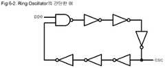
도 8은 링 오실레이터(ring oscillator)를 도시한 회로도.8 is a circuit diagram illustrating a ring oscillator.
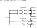
도 9는 종래기술에 따른 펌프 컨트롤 로직(pump control logic)을 도시한 회로도 및 파형도.FIG. 9 is a circuit diagram and waveform diagram showing pump control logic according to the prior art. FIG.
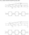
도 10은 종래기술에 따른 크로스 커플 더블 VPP 챠지 펌프(cross coupled doubler VPP charge pump)를 도시한 회로도.10 is a circuit diagram illustrating a cross coupled doubler VPP charge pump according to the prior art.
도 11은 도 10에 도시된 챠지 펌프의 동작 파형도.FIG. 11 is an operational waveform diagram of the charge pump shown in FIG. 10. FIG.
도 12는 종래기술에 따른 트리플러(tripler) VPP 생성회로를 도시한 구성도.12 is a block diagram showing a tripler VPP generation circuit according to the prior art.
도 13은 종래기술에 따른 펌프 컨트롤 로직(pump control logic)을 도시한 회로도.13 is a circuit diagram illustrating pump control logic according to the prior art.
도 14는 도 13에 도시된 펌프 컨트롤 로직의 동작 파형도.FIG. 14 is an operational waveform diagram of the pump control logic shown in FIG.
도 15는 종래기술에 따른 트리플러(tripler) VPP 챠지 펌프를 도시한 회로도.15 is a circuit diagram showing a tripler VPP charge pump according to the prior art.
도 16은 도 15에 도시된 트리플러 VPP 챠지 펌프의 동작 파형도.FIG. 16 is an operational waveform diagram of the tripler VPP charge pump shown in FIG. 15. FIG.
도 17은 본 발명의 바람직한 실시예에 따른 레벨 비교기(level comparator)를 이용한 VPERI 챠지 펌프를 도시한 구성도.17 is a block diagram illustrating a VPERI charge pump using a level comparator according to a preferred embodiment of the present invention.
도 18은 본 발명의 실시예에 따른 레벨 비교기의 상세 회로도.18 is a detailed circuit diagram of a level comparator according to an embodiment of the present invention.
도 19는 본 발명의 또 다른 실시예에 따른 레벨 비교기의 상세 회로도.19 is a detailed circuit diagram of a level comparator according to another embodiment of the present invention.
본 발명은 반도체 기술에 관한 것으로, 특히 본 발명은 반도체 메모리 소자인 DRAM에서 외부 전원인 VCC와 VSS를 각각 VCC보다 높은 전위와 VSS 보다 낮은 전위로 만들어 사용하기 위한 챠지 펌핑(Charge Pumping) 방식의 내부 전원 발생장치에 관한 것이다.BACKGROUND OF THE
반도체 메모리 소자인 디램에서는 오래전부터 외부 전원으로 전위가 서로 다른 내부 전원들을 만들어 그 목적에 따라 다르게 사용하여 오고 있다. 이렇게 외부 전원을 가지고 내부 전원을 만드는 방식에는 크게 두 가지가 있는데, 하나는 외부 전원을 낮은 전위로 다운 컨버팅(down converting)하여 내부 전위를 만들어 사용하는 방식이고 다른 하나는 챠지 펌프(charge pump)를 이용하여 외부 전원 전위보다 높거나 혹은 접지 전위보다 낮은 내부 전위를 만들어 사용하는 방식이다. 일반적으로 다운 컨버팅(Down converting)하여 만든 내부 전원은 전력 소비를 줄이기 위한 것이며, 챠지 펌핑(charge pumping)을 하여 만든 내부 전원은 다음과 같이 특수한 목적에 의한 것이다.In the semiconductor memory device, DRAM, internal power sources having different potentials from external power sources have been used and used differently according to their purpose. There are two ways to make an internal power source with an external power source. One method is to use an internal power source by down converting the external power source to a low electric potential, and the other is using a charge pump. By using this method, an internal potential higher than the external power supply potential or lower than the ground potential is used. In general, internal power generated by down converting is for reducing power consumption, and internal power generated by charge pumping is for a special purpose as follows.
챠지 펌핑(Charge pumping)에 의하여 만들어진 내부 전원 중 DRAM에 가장 보편적으로 사용되고 있는 내부 전원으로는 VPP와 VBB가 있는데, VPP는 셀을 억세스하기 위해 셀 트랜지스터의 게이트(또는, Word Line) 에 셀 데이터의 loss가 없도록 외부 전위인 VCC보다 높은 전위를 만들어 인가하며, VBB는 셀에 저장되어 있는 데이터의 손실을 막기 위해 셀 트랜지스터의 벌크에 외부 전위인 VSS보다 낮은 전위를 만들어 사용한다.Among the internal power sources created by charge pumping, the most commonly used internal power sources for DRAM are VPP and VBB. VPP is a method of accessing a cell to a gate (or word line) of a cell transistor to access a cell. A potential higher than the external potential VCC is applied to prevent loss, and VBB uses a potential lower than the external potential VSS in the bulk of the cell transistor to prevent loss of data stored in the cell.
최근 들어 외부 전원이 1.5V 이하로 낮아짐에 따라서 종래의 기술에서 전력을 줄이기 위해 외부 전원을 다운 컨버팅(down converting)하여 사용하던 내부 전원들의 전위로는 회로의 동작 자체가 불가능해지는 경우가 발생하고 있다. 그 한 예를 도 1에 나타내었다. 도 1에 (a)는 Bit Line Sense Amplifier(이하 BLSA)에서 Bit Line(이하 BL)과 BL bar(이하 /BL)을 equalize 시키는 Bit Line Equalizing(이 하 BLEQ) 트랜지스터의 게이트 control의 pull up 전위로 외부 전원 전위나 그보다 낮은 전위를 사용할 경우에는 BL과 /BL이 제대로 equalize가 되지 않는다.Recently, as the external power supply is lowered to 1.5V or less, there is a case where the operation of the circuit itself becomes impossible by the potential of the internal power supplies that are used by down converting the external power supply to reduce the power in the prior art. . One example is shown in FIG. 1A shows a pull up potential of a gate control of a Bit Line Equalizing (BLEQ) transistor that equalizes a Bit Line (BL) and a BL bar (hereinafter, BL) in a Bit Line Sense Amplifier (hereinafter, BLSA). When using an external power supply potential or lower potential, BL and / BL are not equalized properly.
또한, 이는 도 1의 (b)에 나타낸 것과 같이 Sense Amplifier(이하 SA)에서 SA의 동작 과정 중에 SA의 pull up 트랜지스터인 RTO와, pull down 트랜지스터인 SB를 동작 시키기 전에 이들을 VBLP level로 prechage 시키는 트랜지스터의 control 신호의 pull up source로 사용되는 전위도 외부 전원이나 이보다 낮은 전원으로 사용할 경우도 prechage 동작을 제대로 수행하지 못한다.In addition, as shown in (b) of FIG. 1, the Sense Amplifier (hereinafter referred to as SA) is a transistor that prechages the RTO, which is a pull-up transistor of SA, and the VBLP level before operating the pull-down transistor, SB, during the operation of SA. Even if the potential used as the pull-up source of the control signal of an external power supply or lower power supply does not perform the prechage operation properly.
마지막으로 도 1의 (c)에 나타낸 것과 같이 signal line과 local i/o line , local i/o line과 global i/o line들 사이를 precharge 시켜주는 트랜지스터의 게이트 control 신호의 pull up source로 사용되는 전위도 외부 전원이나 이보다 낮은 전원으로 사용할 경우 이 역시 prechage 동작을 제대로 수행하지 못한다. 이들은 모두 NMOS의 특성상 high level 전달이 어려워 게이트 전위가 drain 전위보다 vth이상 높지 않은 경우 source 전위가 drain에 인가되는 경우 drain 전위는 source 전위에서 vth 만큼의 loss가 발생하기 때문이다.Finally, as shown in (c) of FIG. 1, a pull-up source of a gate control signal of a transistor that precharges a signal line and a local i / o line, a local i / o line, and a global i / o line is used. If the potential is also used with an external power source or lower power supply, this also does not perform the prechage operation properly. This is because when the source potential is applied to the drain when the gate potential is not higher than the drain potential because the high level transfer is difficult due to the characteristics of the NMOS, the drain potential causes the loss as much as vth from the source potential.
이와 같은 문제점을 해결하기 위한 한가지 방법으로 도 2와(종래의 기술1) 같이 charge pump를 이용해 외부 전원 전위보다 높은 전위로 charge pumping하여 만든 내부 전원인 VPP를 다시 한번 down converting하여 외부 전원 전위보다는 높고 내부 전원 VPP 보다는 낮은 VPERI(여기서는 이를 VPERI라 하겠다.)로 만들어 사용하는 경우를 나타내었다. 그러나 이런 방법을 사용할 경우 일반적으로 charge pump의 efficiency가 낮은 원인으로 인해 내부 전원인 VPP를 형성하는데 많은 소모 전류가 필요할 뿐만 아니라 이를 down converting하는 데에도 소모 전류가 필요하기 때문에 2중으로 전류를 소모하게 되어 소모 전류 측면에서 큰 문제가 된다.As a way to solve this problem, as shown in Fig. 2 (prior art 1), the VPP, which is an internal power source made by charge pumping to a potential higher than the external power supply potential using a charge pump, is once again higher than the external power supply potential. In this case, a lower VPERI (hereafter referred to as VPERI) than the internal power supply VPP is used. However, this method generally consumes twice as much current to form internal power supply VPP due to the low efficiency of charge pump and also consumes current to down convert it. This is a big problem in terms of current consumption.
위와 같은 소모 전류 문제를 해결하기 위해서는 도 3과(종래의 기술2) 같이 VPERI 전원을 만들기 위해 charge pump를 따로 구성하여 이를 이용해 VPERI 전원을 만들어 사용하는 경우가 있다. 이것이 도 2와 같은 방식보다 소모 전류 측면에서는 유리하다.(이것에 대한 정량적인 설명은 마지막 부분에서 다루겠다.) 그러나 이 역시 VPERI의 전원이 VPP보다 먼저 형성되는 상황을 발생시켜 latch up 문제를 야기시킨다.In order to solve the above power consumption problem, a charge pump may be separately configured to use a VPERI power supply to make a VPERI power supply as shown in FIG. 3 (prior art 2). This is advantageous in terms of current consumption than in Figure 2 (the quantitative explanation for this is discussed in the last section). However, this also creates a situation where the VPERI's power is formed before VPP, causing latch-up problems. Let's do it.
이는 목표전위는 VPP가 VPERI보다 높지만 VPP의 경우 사용처가 많아 (WL biasing 뿐만 아니라 well의 pick up 용으로도 사용함.) VPP용 reservoir capacitor와 parasitic capacitor의 크기가 상대적으로 작은 VPERI보다 늦게 목표 전위에 도달하게 되고 이렇게 될 경우 도 4에서와 같은 구조에 VPERI에서 VPP로 PN diode가 turn on 되어 current가 흐르게 되고 이에 의해 triggered된 PNP 및 NPN 트랜지스터에 의해 latch up에 빠질 수 있게 되는 것이다.This means that VPP is higher than VPERI, but there are many uses for VPP (not only for WL biasing but also for pick-up of wells). In this case, the PN diode is turned on from VPERI to VPP in the structure as shown in FIG. 4 so that current flows and latches up by the triggered PNP and NPN transistors.
아래에 종래의 기술의 이해와 정량적 설명을 위해 VPERI driver 그리고 Double Charge Pump 및 Triple Charge Pump를 사용한 VPP generator를 차례로 설명하여 보겠다.For the purpose of understanding and quantitative explanation of the prior art, we will describe the VPPP driver and VPP generator using Double Charge Pump and Triple Charge Pump in order.
[VPERI 드라이버(driver)][VPERI driver]
도 5에 VPP를 source 전원으로 하여 이를 down converting하여 VPERI를 만드는 VPERI driver의 한 예를 나타내었다. 그리고 이의 회로의 동작을 간단하게 설명 해보면 다음과 같다. 기준 전위인 vrefp와 VPERI의 전위의 반인 VPERI_HALF를 current mirror로 비교하여 vrefp가 VPERI_HALF보다 높으면 dvr node를 낮추어 VPP로부터 VPERI로 전류를 공급하고 vrefp가 VPERI_HALF보다 낮으면 drv node를 높여 VPP로 부터 VPERI로 공급되는 전류를 차단하는 방식으로 vrefp*2=VPERI를 만족할 때까지 계속 동작하는 회로이다.5 shows an example of a VPERI driver for making a VPERI by down converting the VPP as a source power source. And briefly explain the operation of the circuit as follows. Compare the reference potential vrefp and VPERI_HALF, which is half of the potential of VPERI, with the current mirror.If vrefp is higher than VPERI_HALF, lower the dvr node to supply current from VPP to VPERI. It is a circuit that keeps operating until vrefp * 2 = VPERI is satisfied by blocking current.
[더블 챠지 펌프(double charge pump)][Double charge pump]
도 6은 종래의 VPP generator의 회로구성도이다.6 is a circuit diagram of a conventional VPP generator.
VPP level detector는 level shifter의 출력을 입력으로 하여 VPP level 을 detecting 한다.The VPP level detector detects the VPP level using the output of the level shifter.
Ring Oscillator는 Level Detector 출력 신호를 입력으로 하여 주기 신호를 만들어 낸다.Ring Oscillator generates a periodic signal by inputting the Level Detector output signal.
pump Control Logic는 ring osc 출력 신호를 이용하여 pump control 하는 신호를 만들어 낸다.The pump control logic uses the ring osc output signal to generate the pump control signal.
Charge Pump는 VPP를 만든다.Charge Pump creates VPP.
기존에 사용했던 VPP level detector의 간단한 예를 도 7에 도시하였다. VPP를 만들기 위해 가져다 쓰는 Vref를 하나의 입력으로 하여 기준전압으로 삼아준다. 그리고 VPP를 다시 feedback input으로 받아서 Vref와 node A의 level을 비교하여 판단을 내려주게 된다. 즉 VPP가 원하는 target voltage 보다 떨어지게 되면 직렬로 연결된 저항들의 한 node인 node A의 level이 Vr1보다 낮아지게 되고 이는 출력 신호 ppe를 high로 만들어주게 된다. 그리고 VPP가 target level 과 같거나 높아지 게 되면 node A가 Vref보다 높아져서 결과적으로 출력신호 ppe를 low로 만들어준다. 그리고 VPP의 target voltage 를 높여주거나 낮추어줄 필요가 있을 경우는 그림에서의 fuse를 cutting함으로 node A의 양단 저항 비를 달리해줌으로써 조정해 줄 수도 있다.A simple example of a conventional VPP level detector is shown in FIG. 7. Use Vref as the input to make VPP as the reference voltage. The VPP is received again as a feedback input and the judgment is made by comparing the levels of Vref and node A. That is, when VPP falls below the desired target voltage, the level of node A, a node of the series connected resistors, becomes lower than Vr1, which makes the output signal ppe high. When VPP is equal to or higher than the target level, node A becomes higher than Vref, resulting in low output signal ppe. If you need to increase or decrease the target voltage of VPP, you can adjust by changing the resistance ratio of both ends of node A by cutting fuse in the figure.
여기서 ppe는 도 8에서 ring oscillator를 동작하도록 만들어주는 신호로서 high일 때 ring oscillator가 동작을 하게 된다. 그리고 ring oscillator가 동작하게 되면 도 9와 같이 pump control logic에 의해 p1, p2, g1, g2신호가 발생되고 이는 도 10의 charge pump에 입력되어 pump를 동작시키고 VPP의 level을 높여주게 된다. 이 후 pumping이 지속되어 VPP가 target level에 도달하게 되면 VPP level detector에서 이 level을 감지하여 ppe를 low로 만들어 pumping을 중단시킨다. 이러한 일련의 동작으로 pumping된 charge는 VPP와 VSS사이에 Cap을 달아 저장하게 되며 평균적으로 일정한 level을 유지하게 되고 WL을 구동하기 위해 사용하게 된다. 만약 WL을 구동하여 이 Cap에 저장된 전류를 소모하게 되면 VPP level은 낮아지게 되고, 이렇게 되면 VPP level detector는 이를 감지하여 다시 ppe를 high로 enable시킨다.Here, ppe is a signal for operating the ring oscillator in Figure 8 when the ring oscillator is operating when high. When the ring oscillator is operated, p1, p2, g1, and g2 signals are generated by the pump control logic as shown in FIG. 9, which is input to the charge pump of FIG. 10 to operate the pump and increase the level of the VPP. After the pumping is continued and the VPP reaches the target level, the VPP level detector detects this level and stops pumping by making ppe low. In this series of operations, the pumped charge is stored with a cap between VPP and VSS, and maintains a constant level on average and is used to drive WL. If WL is consumed and the current stored in this Cap is consumed, the VPP level is lowered. Then, the VPP level detector detects this and enables ppe high again.
도 9의 Control logic에서 만들어진 p1, p2, g1, g2가 도 10의 charge pump에 입력되게 되면, 그 timing diagram에서도 알 수 있듯이 p1이 VSS에서 VCC로 transition하는 순간에 p1boot은 bootstrapping되어 VCC에서 2VCC로 transition하게 되고, 이 순간에 p2는 VCC에서 VSS로 transition하여 p2boot은 bootstrapping되어 2VCC에서 VCC로 transition된다. 이렇게 되면 2VCC level인 p1boot의 charge 가 transfer transistor인 P1을 통해 VPP로 들어가게 된다. 이렇게 얼마간의 시간 동안 p1boot과 VPP는 charge sharing을 하여 equilibrium 상태에 도달하게 된다. 이후 g2가 VSS에서 VCC로 transition하여 g2boot이 bootstrapping되어 VCC에서 2VCC가 되면 N2가 turn on 되어 p2boot을 VCC로 pre-charge를 하게 되고 다시 g2가 VCC에서 VSS로 transition하여 g2boot이 VCC가 되어 N2가 turn off 되어 pre-charge가 완료되면 p1은 VCC에서 VSS로 transition하여 p1boot을 VCC로 만들고 p2는 VSS에서 VCC로 transition하여 p2boot을 2VCC로 만들게 되어 이번에는 transfer transistor P2를 통해서 p2boot과 VPP사이에 charge sharing이 이루어 진다.When p1, p2, g1, and g2 generated in the control logic of FIG. 9 are input to the charge pump of FIG. 10, as shown in the timing diagram, p1boot bootstrapping at the moment p1 transitions from VSS to VCC, and then from VCC to 2VCC. At this moment p2 transitions from VCC to VSS and p2boot bootstrapping to transition from 2VCC to VCC. In this case, the charge of p1boot at the 2VCC level enters VPP through the transfer transistor P1. During this time, p1boot and VPP reach equilibrium with charge sharing. After g2 transitions from VSS to VCC and g2boot bootstrapping and becomes 2VCC in VCC, N2 is turned on and p2boot is precharged to VCC, then g2 transitions from VCC to VSS and g2boot becomes VCC and N2 turns When the pre-charge is off, p1 transitions from VCC to VSS to make p1boot VCC and p2 transitions from VSS to VCC to make p2boot 2VCC. This time, charge sharing between p2boot and VPP is transferred through transfer transistor P2. Is done.
이렇게 또다시 얼마간의 시간이 흘러 p2boot과 VPP가 charge sharing을 하여 equilibrium 상태에 도달하게 되면, 이번에는 g1이 VSS에서 VCC로 transition하여 g1boot이 bootstrapping되어 VCC에서 2VCC가 되면 N1이 turn on 되어 p1boot을 VCC로 pre-charge를 하게 되고 다시 g1이 VCC에서 VSS로 transition하여 g1boot이 VCC가 되어 N1이 turn off 되어 pre-charge가 완료되어 다음 동작을 준비하게 된다.After some time, when p2boot and VPP reach the equilibrium state by charge sharing, this time, g1 transitions from VSS to VCC, g1boot bootstrapping, and when VCC is 2VCC, N1 is turned on and p1boot is VCC. After the pre-charge, g1 transitions from VCC to VSS, g1boot becomes VCC, N1 turns off, and the pre-charge is completed, preparing for the next operation.
도 11은 앞에서 언급했던 VPP pump의 동작의 이해를 돕기 위해 control timing과 p1boot, p2boot 그리고 VPP node를 과장해서 그린 그림이다. 그림에서도 알 수 있듯이 p1boot과 p2boot node는 최대 2VCC까지 밖에 bootstrapping 되지 못하며 pre-charge도 VCC까지 밖에는 안 되는 것을 알 수 있다. 결과적으로 VPP도 최대 2VCC까지밖에 갈 수 없다는 것을 알 수 있다. 어쨌든 이런 일련의 과정을 통해 VPP charge pump는 VCC에서 VPP로 charge를 공급하게 된다.FIG. 11 is an exaggerated drawing of control timing, p1boot, p2boot and VPP nodes to help understand the operation of the aforementioned VPP pump. As can be seen from the figure, the p1boot and p2boot nodes are only bootstrapping up to 2VCC and the pre-charge is only up to VCC. As a result, it can be seen that VPP can only go up to 2VCC. In any case, through this sequence, the VPP charge pump supplies charge from VCC to VPP.
일반적으로 doubler VPP charge pump의 current efficiency는 ((2VCC- VPP)*C/2VCC*C)*100이고(여기서 C는 p1boot과 p2boot node의 정전용량이다.), 이론상 최대로 pumping 가능한 VPP level은 2VCC가 된다. 예를 들어 VCC=1.5v이고 VPP target level을 3v라고 하면 current efficiency는 0%이고, VPP target level을 2.0v라고 하면 current efficiency는 33%가 된다. 이론상 최대로 pumping 가능한 VPP level은 3v가 된다. 여기서 current efficiency는 VPP쪽에 저장되는 charge의 양을 VDD쪽에서 공급되는 charge의 양으로 나눈 값이다.In general, the current efficiency of a doubler VPP charge pump is ((2VCC-VPP) * C / 2VCC * C) * 100 (where C is the capacitance of the p1boot and p2boot nodes), and theoretically the maximum pumpable VPP level is 2VCC. Becomes For example, if VCC = 1.5v and the VPP target level is 3v, the current efficiency is 0%. If the VPP target level is 2.0v, the current efficiency is 33%. In theory, the maximum pumpable VPP level is 3v. The current efficiency is the amount of charge stored on the VPP side divided by the amount of charge supplied on the VDD side.
[트리플 챠지 펌프(triple charge pump)][Triple charge pump]
도 12는 종래의 Tripler VPP generator의 회로구성도이다.12 is a circuit diagram of a conventional Tripler VPP generator.
VPP level detector는 level shifter의 출력을 입력으로 하여 VPP level을 detecting 한다. Doubler VPP의 level detector와 동일하다.The VPP level detector detects the VPP level using the output of the level shifter. Equivalent to the Doubler VPP level detector.
Ring Oscillator는 Level Detector 출력 신호를 입력으로 하여 주기 신호를 만들어 낸다. Doubler VPP의 Ring Oscillator와 동일하다.Ring Oscillator generates a periodic signal by inputting the Level Detector output signal. Same as Ring Oscillator of Doubler VPP.
Pump Control Logic은 ring osc 출력 신호를 이용하여 pump control 하는 신호를 만들어 낸다.The Pump Control Logic generates a pump control signal using the ring osc output signal.
Tripler Charge Pump는 VPP를 만든다.Tripler Charge Pump creates VPP.
Tripler VPP Charge Pump가 Doubler VPP Charge의 동작과 다른 점은 Pump Control Logic 부분과 Charge Pump 부분이다. 여기서는 이 두 부분에 대한 설명을 하겠다.The Tripler VPP Charge Pump differs from the Doubler VPP Charge in its Pump Control Logic and Charge Pump sections. This section describes these two parts.
도 13은 Tripler Charge pump용 Control 신호를 만드는 회로이며, Ring Oscillator에서 나온 OSC 신호를 이용하여 g1, g2, g3, p1, p2와 같은 timing을 갖 는 신호를 만들어 도7-4에 있는 Tripler Charge Pump를 동작시키게 된다. 여기서 g1’ , g2’, g3’, p1' p2'는 g1, g2, g3, p1, p2와 같은 timing을 갖는 신호이며 위상만 반대이다. 이 두 그룹의 신호들은 그림5-5와 같은 형태로 구성된 Tripler VPP Charge Pump에 입력되어 VPP를 발생시키게 한다.FIG. 13 is a circuit for making a control signal for a tripler charge pump, and a signal having a timing such as g1, g2, g3, p1, and p2 is generated using an OSC signal from a ring oscillator, and the tripler charge pump shown in FIGS. Will be activated. Here, g1 ', g2', g3 ', and p1' p2 'are signals having timings such as g1, g2, g3, p1, and p2, except that the phase is reversed. Signals from these two groups are input to a Tripler VPP Charge Pump configured as shown in Figure 5-5 to generate VPP.
도 14는 Tripler VPP Charge Pump를 나타내고 있다.14 shows a Tripler VPP Charge Pump.
동작은 g1이 VSS에서 VCC로 transition해서 N1을 turn on 시키고, 이때 p1이 VCC에서 VSS로 transition하여 p1boot이 VCC로 가면 p1boot은 VCC와 pre-charge하여 VCC가 된다.Operation g1 transitions from VSS to VCC and turns on N1. At this time, if p1 transitions from VCC to VSS and p1boot goes to VCC, p1boot is precharged with VCC to become VCC.
이후 g1이 VCC에서 VSS로 transition해서 P1을 turn off시키고, 이때 p1이 VSS에서 VCC로 transition하여 p1boot이 2VCC로 간 상태에서 g2가 VSS에서 VCC로 transition하여 N2를 turn on 시킨다. 이때 p2는 VCC에서 VSS로 transition하여 p2boot을 -VCC로 만든다. 이후 p2boot은 p1boot과 pre-charge하여 VCC로 간다. 그리고 g2가 VCC에서 VSS로 transition하면 P2는 turn off되고, p2는 다시 VSS에서 VCC로 transition하 p2boot을 2VCC로 만든다. 마지막으로 g3가 VSS에서 VCC로 transition하면서 N3를 turn on 시키면 VPP는 2VCC인 p2boot과 Charge Sharing을 하게 된다. 이런 일련의 동작으로 p1boot은 최대 2VCC까지 charge pumping이 가능하고 p2boot은 3VCC까지 charge pumping이 가능하다. 그리고 g1 , g2' g3' p1' p2'는 g1, g2, g3, p1, p2와 반대 위상을 가지고 위와 동일한 방식으로 pumping을 한다. 즉, cross coupled되어 있는 Tripler VPP Charge Pump는 번갈아 가며 VPP에 charge를 공급하게 되는 것이다.Then, g1 transitions from VCC to VSS and turns off P1. At this time, when p1 transitions from VSS to VCC, p1boot goes to 2VCC, g2 transitions from VSS to VCC and turns on N2. P2 transitions from VCC to VSS to make p2boot -VCC. P2boot then precharges p1boot to VCC. When g2 transitions from VCC to VSS, P2 is turned off, p2 transitions from VSS to VCC again and makes p2boot 2VCC. Finally, when g3 transitions from VSS to VCC and turns on N3, VPP will have 2VCC p2boot and Charge Sharing. This series of operations allows p1boot to charge pumping up to 2VCC and p2boot to charge pumping up to 3VCC. And g1, g2 'g3' p1 'p2' is pumped in the same manner as above with the phase opposite to g1, g2, g3, p1, p2. In other words, the triple coupled VPP charge pump alternately supplies charge to the VPP.
그러나, 종래의 Tripler VPP Charge Pump역시 p1boot과 p2boot은 pre-charge level이 각각 VCC와 2VCC 이므로 최대 pumping 가능한 level은 각각 2VCC와 3VCC가 된다.However, in the conventional Tripler VPP Charge Pump, p1boot and p2boot also have a maximum charge level of 2VCC and 3VCC since the precharge levels are VCC and 2VCC, respectively.
도 16은 앞에서 언급했던 VPP pump의 동작의 이해를 돕기 위해 control timing과 VPP level을 과장해서 나타낸 도면으로 p1boot, p1’boot node에서 일어나는 동작과 p2boot, p2’boot node에서 일어나는 동작을 구분 지어 그렸다. 도시된 바와 같이, p1boot과 p1’boot node는 최대 2VCC까지 밖에 bootstrapping 되지 못하며 pre-charge도 VCC까지 밖에는 안 되는 것을 알 수 있다. 그리고 p2boot과 p2’boot node는 최대 3VCC까지 밖에 bootstrapping 되지 못하며 pre-charge도 2VCC까지 밖에는 안 되는 것을 알 수 있다. 결과적으로 p2boot과 p2’boot에서 만들 수 있는 VPP level은 최대 3VCC까지밖에 갈 수 없다는 것을 알 수 있다. 어쨌든 이런 일련의 과정을 통해 VPP charge pump는 VCC에서 VPP로 charge를 공급하게 된다.FIG. 16 is a diagram showing an exaggerated control timing and VPP level for better understanding of the operation of the aforementioned VPP pump, and distinguishes the operation occurring at the p1boot and p1'boot nodes and the operation occurring at the p2boot and p2'boot nodes. As shown, it can be seen that the p1boot and p1 'boot nodes are only bootstrapping up to 2VCC and the pre-charge is only up to VCC. The p2boot and p2 'boot nodes are only bootstrapping up to 3VCC and the pre-charge is only 2VCC. As a result, we can see that the VPP level that can be created in p2boot and p2'boot can only go up to 3VCC. In any case, through this sequence, the VPP charge pump supplies charge from VCC to VPP.
일반적으로 Tripler VPP charge pump의 current efficiency는 ((3VCC- VPP)*C/5VCC*C)*100이고(여기서 C는 p1boot과 p1’boot 그리고 p2boot과 p2’boot node의 정전용량이다.), 이론상 최대로 pumping 가능한 VPP level은 3VCC가 된다. 예를 들어 VCC=1.5v이고 VPP target level을 3.0v라고 하면 current efficiency는 20%이고, VPP target level을 2.0v라고 하면 current efficiency는 33%가 된다. 그리고 이론상 최대로 pumping 가능한 VPP level은 4. 5v가 된다. 여기서 current efficiency는 VPP쪽에 저장되는 charge의 양을 VDD쪽에서 공급되는 charge의 양으 로 나눈 값이다.In general, the current efficiency of the Tripler VPP charge pump is ((3VCC-VPP) * C / 5VCC * C) * 100 (where C is the capacitance of p1boot and p1'boot and p2boot and p2'boot nodes), in theory. The maximum pumpable VPP level is 3VCC. For example, if VCC = 1.5v and the VPP target level is 3.0v, the current efficiency is 20%. If the VPP target level is 2.0v, the current efficiency is 33%. In theory, the maximum pumpable VPP level is 4.5v. The current efficiency is the amount of charge stored on the VPP side divided by the amount of charge supplied on the VDD side.
위에서 설명한 바와 같이 triple pump를 사용하여 3.0V의 VPP를 만들고 이를 driver를 사용하여 VPERI를 만드는 경우, VPP pump의 efficiency가 20% 정도 이므로 20mA의 IPP를 만들기 위해서는 80mA의 소모 전류가 필요하다. 이후 이 20mA의 IPP 중 10mA를 IPERI로 만드는 경우 efficiency는 거의 90%(10mA를 구동하기 위해서 소모되는 전륜는 1mA 이하이다.) 이상이기 때문에 총 소모 전류는 대략 81mA 정도이다.As described above, when making VPP of 3.0V by using triple pump and VPERI by using driver, 80mA consumption current is needed to make 20mA IPP because VPP pump efficiency is about 20%. If we make 10 mA of this 20mA IPP as IPERI, the efficiency is almost 90% (the front wheel consumes less than 1mA to drive 10mA), so the total current consumption is approximately 81mA.
다음으로 triple pump를 이용하여 3.0V의 VPP를 만들고 double 이나 triple pump를 이용해서 VPERI를 만드는 경우, VPP pump의 efficiency가 20% 정도 이므로 10mA의 IPP를 만들기 위해서는 40mA의 소모 전류가 필요하다. 그리고 VPERI pump의 efficiency가 30% 정도 이므로 10mA의 IPERI를 만들기 위해서는 33mA의 소모 전류가 필요하다. 그러므로 이때 10mA의 IPP와 10mA의 IPERI를 만들기 위해서 소모된 전류는 73mA 정도이다.Next, when making VPP of 3.0V using triple pump and VPERI using double or triple pump, 40mA current consumption is required to make 10mA IPP because the efficiency of VPP pump is about 20%. Since the efficiency of the VPERI pump is about 30%, a current consumption of 33mA is required to make a 10mA IPERI. Therefore, the current consumed to make 10mA IPP and 10mA IPERI is about 73mA.
마지막으로 VPERI를 double pump로 구성할 것인지 triple pump로 구성할 것인지는 VPERI target level이 얼마이냐에 따라서 결정하면 된다. 예를 들어 VPERI가 2.0V보다 높다면 triple pump를 사용하는 것이 그 반대의 경우는 double pump를 사용하는 것이 유리하며 2.0V인 경우에는 두 pump의 효율이 같으므로 어떤 것을 사용하여도 무방하다 하겠다. 하지만 면적 측면에서 double pump가 유리하므로 위의 경우 double pump를 사용하는 것이 좋다. Finally, whether VPERI is configured as a double pump or triple pump depends on the VPERI target level. For example, if VPERI is higher than 2.0V, it is advantageous to use a triple pump and vice versa. If it is 2.0V, the efficiency of the two pumps is the same. However, the double pump is advantageous in terms of area, so it is better to use the double pump in the above case.
정량적인 계산에서도 알 수 있듯이 latch up 문제만 해결 할 수 있다면 종래 의 기술2가 소모 전류 측면에서 더 유리하다는 것을 알 수 있고, 이런 구조들이 다수로 들어있는 경우 종래의 기술2는 더욱 유리하다 하겠다.As can be seen from the quantitative calculation, if only the latch-up problem can be solved, it can be seen that the conventional technique 2 is more advantageous in terms of current consumption, and the conventional technique 2 is more advantageous when these structures are included in a large number.
따라서, 본 발명은 상기한 문제점을 해결하기 위하여 안출된 것으로서, 종래의 기술2에서와 같이 내부전원인 VPP와 VPERI를 형성함에 있어 각각 charge pump를 사용하는 경우 초기 이들 내부 전원의 전위차에 의해 발생할 수 있는 latch up 문제를 해결하고자 하는 것이다.Accordingly, the present invention has been made to solve the above-mentioned problems, and when the charge pump is used to form the internal power supply VPP and VPERI as in the conventional technique 2, it may be caused by the potential difference between these internal power supplies. We want to solve the latch up problem.
본 발명에서는 이를 해결하기 위하여 도 17에 나타낸 개념도와 같이 VPP와 VPERI의 전위를 감지하여 VPP가 VPERI보다 높은 경우에 High를 그 반대의 경우에 Low를 출력하는 Level Comparator 회로를 두고 이 신호를 VPERI Detector의 출력과 NAND의 입력으로 받아서 VPERI의 pump를 control하는 것이다. 이렇게 하면 VPERI pump의 동작은 VPERI가 VPP보다 낮을 때에만 동작을 하게 되어 latch up 문제를 해결할 수 있는 것이다.In order to solve this problem, the present invention has a level comparator circuit that detects the potential of VPP and VPERI and outputs low when VPP is higher than VPERI and low when vice versa, as shown in the conceptual diagram of FIG. 17. It is to control VPERI's pump by receiving output and NAND input. This allows the VPERI pump to operate only when VPERI is lower than VPP, thus solving the latch up problem.
본 발명은 charge pumping 방식을 사용하여 외부 전원 전위보다 높은 두 종류 이상의 내부 전원을 만들어 사용하는 경우 발생할 수 있는 latch up 문제를 해결하기 위해 각각의 charge pump로 만든 내부전원들 사이에 level comparator를 두어 전원 형성 시점을 조절한다.The present invention provides a level comparator between internal power sources made of each charge pump to solve the latch up problem that may occur when using two or more types of internal power sources higher than the external power potential using the charge pumping method. Adjust the time of formation.
또한, 본 발명은 상기 charge pump를 이용하여 두 종류 이상의 내부 전원을 형성할 때 이들 내부 전원을 비교하기 위해 level comparator를 두는 모든 구조 및 장치을 제공한다.In addition, the present invention provides all the structures and devices that have a level comparator to compare the internal power when forming two or more types of internal power using the charge pump.
또한, 본 발명은 level comparator의 출력을 받아 이를 내부 전원의 detector에서 나온 enable 신호와 Summation을 하여 상대적으로 전위가 낮은 내부 전원을 만드는 charge pump의 동작 시점을 조절하는 모든 구조 및 장치를 제공한다.In addition, the present invention provides all the structures and devices for adjusting the operation time of the charge pump that receives the output of the level comparator and makes a summation with the enable signal from the detector of the internal power source to make the internal power source with a relatively low potential.
또한, 본 발명은 level comparator는 각각 비교하고자 하는 내부 전원과 접지 전원 사이에 diode divider를 두어 비교를 위한 내부 전원의 전위를 dividing level을 검출하며, 이를 current mirror type의 static이나 dynamic buffer등과 같은 comparator의 두 입력으로 물려 그 출력을 만드는 모든 구조 및 장치를 제공한다.In addition, the present invention, the level comparator has a diode divider between the internal power source and the ground power source to be compared, respectively, to detect the level of dividing the potential of the internal power source for comparison, and the comparator such as a static mirror or dynamic buffer of the current mirror type It provides all the structures and devices that are fed into the two inputs and make that output.
또한, 본 발명은 level comparator를 구성함에 있어 diode divider 대신 저항 divider를 사용하는 경우로 각각 비교하고자 하는 내부 전원과 접지 전원 사이에 저항을 직렬 연결하고 전위 비교를 위한 dividing level을 검출하여, 이를 이를 current mirror type의 static이나 dynamic buffer등과 같은 comparator의 두 입력으로 물려 그 출력을 만드는 모든 구조 및 장치를 제공한다.In addition, the present invention uses a resistor divider instead of a diode divider in the configuration of a level comparator, respectively connecting a resistor between the internal power supply and the ground power supply to be compared in series and detects the dividing level for potential comparison, and this is the current It provides all the structures and devices that make up the output by taking two inputs from a comparator such as a mirror type static or dynamic buffer.
이하, 본 발명이 속하는 기술분야에서 통상의 지식을 가진 자가 본 발명의 기술적 사상을 용이하게 실시할 수 있을 정도로 상세히 설명하기 위하여, 본 발명 의 가장 바람직한 실시 예를 첨부한 도면을 참조하여 설명한다.DETAILED DESCRIPTION Hereinafter, exemplary embodiments of the present invention will be described with reference to the accompanying drawings so that those skilled in the art may easily implement the technical idea of the present invention.
본 발명의 전반적인 구성은 종래의 기술2와 유사하다 다만 VPERI pump를 동작시킴에 있어 VPP와 VPERI의 전위를 비교하여 VPP가 VPERI보다 높을 때에 High를 출력하고, 그 반대의 경우 Low를 출력하도록 도 18과 같이 Level Comparator를 구성하였다. 그리고 그 동작을 설명하여 보면 다음과 같다. VPP와 접지 전위 VSS 사이에 diode로 구성된 divider가 있어 A node의 전위는 VPP의 1/3이 되며, VPERI와 접지 전위 VSS 사이에도 이와 동일한 diode divider가 있어 B node의 전위는 VPERI의 1/3가 된다. current mirror로 구성된 comparator는 이 A와 B node의 전위를 비교하여 출력으로 A가 B보다 높으면 High를 그 반대의 경우이면 Low를 출력하게 되어 이 신호가 VPERI detector에서 나온 enable 신호와 NAND의 입력으로 물력서 VPERI의 pump의 동작 시점을 조절하게 되는 것이다. 나머지 동작은 앞서 설명했던 것과 같은 charge pump의 동작과 같으므로 생략하겠다. 또한, 도 19와 같이 저항 divider를 이용하여 level comparator를 구성하는 것도 가능하다.The overall configuration of the present invention is similar to that of the related art 2. However, the operation of the VPERI pump compares the potential of VPP and VPERI to output High when VPP is higher than VPERI, and vice versa. Level Comparator is configured as follows. The operation is described as follows. There is a divider consisting of diodes between VPP and ground potential VSS, so that the potential of A node is 1/3 of VPP, and the same diode divider is present between VPERI and ground potential VSS, so that the potential of B node is 1/3 of VPERI. do. The comparator composed of the current mirror compares the potential of this A and B nodes and outputs high when A is higher than B, and low when vice versa. This signal is used as the enable signal from the VPERI detector and the input of NAND. This is to control the operation time of VPERI pump. The rest of the operation is the same as that of the charge pump as described above, and thus will be omitted. Also, as shown in FIG. 19, a level comparator may be configured using a resistor divider.
물론 VPERI의 reservoir capacitor를 VPP의 reservoir capacitor보다 아주 크게 만들어도 이와 같은 효과를 가져올 수도 있으나 control timing이 불명확하고 면적적으로도 손해이기 때문에 본 발명의 기술이 유리하다 하겠다. Of course, even if the reservoir capacitor of VPERI is much larger than the reservoir capacitor of VPP may have the same effect, but the technique of the present invention is advantageous because the control timing is unclear and area damage.
본 발명의 기술 사상은 상기 바람직한 실시예에 따라 구체적으로 기술되었으나, 상기한 실시예는 그 설명을 위한 것이며 그 제한을 위한 것이 아님을 주의하여야 한다. 또한, 본 발명의 기술 분야의 통상의 전문가라면 본 발명의 기술 사상의 범위 내에서 다양한 실시예가 가능함을 이해할 수 있을 것이다.Although the technical idea of the present invention has been described in detail according to the above preferred embodiment, it should be noted that the above-described embodiment is for the purpose of description and not of limitation. In addition, those skilled in the art will understand that various embodiments are possible within the scope of the technical idea of the present invention.
이상에서 설명한 바와 같이, 본 발명에서는 기존 VCORE Discharge Driver의 경우, 설계시 효과적인 방전을 기대하기 어렵고 불량 분석 단계에서 방전시간, 방전용 트랜지스터의 사이즈, 응답속도 등의 튜닝 작업이 필수적으로 요구되었다. 본 발명에서는 대규모 방전에는 보다 높은 기준전압과 짧은 방전시간을 적용하고, 소규모의 안정적인 방전에는 보다 낮은 기준전압과 상대적으로 긴 방전시간을 적용하여 방전동작의 효율성과 안정성을 확보할 수 있다.As described above, in the present invention, in the case of the existing VCORE Discharge Driver, it is difficult to expect an effective discharge during the design, and tuning work such as discharge time, size of the transistor for discharging, response speed, etc. is required in the failure analysis step. In the present invention, a higher reference voltage and a shorter discharge time may be applied to a large-scale discharge, and a lower reference voltage and a relatively long discharge time may be applied to a small-scale stable discharge to ensure efficiency and stability of the discharge operation.
Claims (1)
Translated fromKoreanPriority Applications (1)
| Application Number | Priority Date | Filing Date | Title |
|---|---|---|---|
| KR1020050091649AKR20070036522A (en) | 2005-09-29 | 2005-09-29 | Charge pump |
Applications Claiming Priority (1)
| Application Number | Priority Date | Filing Date | Title |
|---|---|---|---|
| KR1020050091649AKR20070036522A (en) | 2005-09-29 | 2005-09-29 | Charge pump |
Publications (1)
| Publication Number | Publication Date |
|---|---|
| KR20070036522Atrue KR20070036522A (en) | 2007-04-03 |
Family
ID=38158687
Family Applications (1)
| Application Number | Title | Priority Date | Filing Date |
|---|---|---|---|
| KR1020050091649AWithdrawnKR20070036522A (en) | 2005-09-29 | 2005-09-29 | Charge pump |
Country Status (1)
| Country | Link |
|---|---|
| KR (1) | KR20070036522A (en) |
- 2005
- 2005-09-29KRKR1020050091649Apatent/KR20070036522A/ennot_activeWithdrawn
Similar Documents
| Publication | Publication Date | Title |
|---|---|---|
| US7023260B2 (en) | Charge pump circuit incorporating corresponding parallel charge pump stages and method therefor | |
| US7982530B2 (en) | Internal voltage generating apparatus and method for controlling the same | |
| US7495500B2 (en) | Method for using a multiple polarity reversible charge pump circuit | |
| US5367489A (en) | Voltage pumping circuit for semiconductor memory devices | |
| JP4898373B2 (en) | Internal voltage generation circuit | |
| US20130107650A1 (en) | Semiconductor device having hierarchical bit line structure | |
| US8902691B2 (en) | Semiconductor device having charge pump circuit and information processing apparatus including the same | |
| KR100884340B1 (en) | Internal voltage generator | |
| US20050206440A1 (en) | High voltage generator in semiconductor memory device | |
| JP2005033993A (en) | Charge pump circuit | |
| KR100870429B1 (en) | Internal voltage generation circuit | |
| KR100753124B1 (en) | Internal voltage generating circuit | |
| KR100977731B1 (en) | Negative Wordline Voltage Generators in Semiconductor Memory Devices | |
| US8587366B2 (en) | Semiconductor device | |
| KR100695421B1 (en) | Internal Voltage Generator of Semiconductor Memory Devices | |
| JP4808988B2 (en) | High voltage generation circuit that maintains charge pumping efficiency | |
| KR20070036522A (en) | Charge pump | |
| US8138821B2 (en) | High voltage pumping circuit | |
| US7619946B2 (en) | Active driver for use in semiconductor device | |
| KR100585144B1 (en) | High voltage generation circuit for preserving charge pumping efficiency | |
| US20100052776A1 (en) | Internal voltage generating circuit | |
| KR100780635B1 (en) | Semiconductor memory device and core voltage generation method thereof | |
| JP3987856B2 (en) | Voltage detection circuit, semiconductor device, and voltage detection circuit control method | |
| KR100873622B1 (en) | Bulk voltage generation circuit and semiconductor memory device including same | |
| GB2288678A (en) | Memory including voltage pumping circuit |
Legal Events
| Date | Code | Title | Description |
|---|---|---|---|
| PA0109 | Patent application | Patent event code:PA01091R01D Comment text:Patent Application Patent event date:20050929 | |
| PG1501 | Laying open of application | ||
| PC1203 | Withdrawal of no request for examination | ||
| WITN | Application deemed withdrawn, e.g. because no request for examination was filed or no examination fee was paid |