KR20070029694A - Bipolar semiconductor device and manufacturing method thereof - Google Patents
Bipolar semiconductor device and manufacturing method thereofDownload PDFInfo
- Publication number
- KR20070029694A KR20070029694AKR1020067022103AKR20067022103AKR20070029694AKR 20070029694 AKR20070029694 AKR 20070029694AKR 1020067022103 AKR1020067022103 AKR 1020067022103AKR 20067022103 AKR20067022103 AKR 20067022103AKR 20070029694 AKR20070029694 AKR 20070029694A
- Authority
- KR
- South Korea
- Prior art keywords
- silicon carbide
- substrate
- semiconductor device
- epitaxial
- sic
- Prior art date
- Legal status (The legal status is an assumption and is not a legal conclusion. Google has not performed a legal analysis and makes no representation as to the accuracy of the status listed.)
- Granted
Links
Images


Classifications
- H—ELECTRICITY
- H10—SEMICONDUCTOR DEVICES; ELECTRIC SOLID-STATE DEVICES NOT OTHERWISE PROVIDED FOR
- H10D—INORGANIC ELECTRIC SEMICONDUCTOR DEVICES
- H10D8/00—Diodes
- H10D8/422—PN diodes having the PN junctions in mesas
- H—ELECTRICITY
- H01—ELECTRIC ELEMENTS
- H01L—SEMICONDUCTOR DEVICES NOT COVERED BY CLASS H10
- H01L21/00—Processes or apparatus adapted for the manufacture or treatment of semiconductor or solid state devices or of parts thereof
- H01L21/02—Manufacture or treatment of semiconductor devices or of parts thereof
- H01L21/02002—Preparing wafers
- H01L21/02005—Preparing bulk and homogeneous wafers
- H01L21/02008—Multistep processes
- H01L21/0201—Specific process step
- H01L21/02019—Chemical etching
- H—ELECTRICITY
- H01—ELECTRIC ELEMENTS
- H01L—SEMICONDUCTOR DEVICES NOT COVERED BY CLASS H10
- H01L21/00—Processes or apparatus adapted for the manufacture or treatment of semiconductor or solid state devices or of parts thereof
- H01L21/02—Manufacture or treatment of semiconductor devices or of parts thereof
- H01L21/02002—Preparing wafers
- H01L21/02005—Preparing bulk and homogeneous wafers
- H01L21/02008—Multistep processes
- H01L21/0201—Specific process step
- H01L21/02024—Mirror polishing
- H—ELECTRICITY
- H01—ELECTRIC ELEMENTS
- H01L—SEMICONDUCTOR DEVICES NOT COVERED BY CLASS H10
- H01L21/00—Processes or apparatus adapted for the manufacture or treatment of semiconductor or solid state devices or of parts thereof
- H01L21/02—Manufacture or treatment of semiconductor devices or of parts thereof
- H01L21/02104—Forming layers
- H01L21/02365—Forming inorganic semiconducting materials on a substrate
- H01L21/02367—Substrates
- H01L21/0237—Materials
- H01L21/02373—Group 14 semiconducting materials
- H01L21/02378—Silicon carbide
- H—ELECTRICITY
- H01—ELECTRIC ELEMENTS
- H01L—SEMICONDUCTOR DEVICES NOT COVERED BY CLASS H10
- H01L21/00—Processes or apparatus adapted for the manufacture or treatment of semiconductor or solid state devices or of parts thereof
- H01L21/02—Manufacture or treatment of semiconductor devices or of parts thereof
- H01L21/02104—Forming layers
- H01L21/02365—Forming inorganic semiconducting materials on a substrate
- H01L21/02367—Substrates
- H01L21/02433—Crystal orientation
- H—ELECTRICITY
- H01—ELECTRIC ELEMENTS
- H01L—SEMICONDUCTOR DEVICES NOT COVERED BY CLASS H10
- H01L21/00—Processes or apparatus adapted for the manufacture or treatment of semiconductor or solid state devices or of parts thereof
- H01L21/02—Manufacture or treatment of semiconductor devices or of parts thereof
- H01L21/02104—Forming layers
- H01L21/02365—Forming inorganic semiconducting materials on a substrate
- H01L21/02518—Deposited layers
- H01L21/02521—Materials
- H01L21/02524—Group 14 semiconducting materials
- H01L21/02529—Silicon carbide
- H—ELECTRICITY
- H01—ELECTRIC ELEMENTS
- H01L—SEMICONDUCTOR DEVICES NOT COVERED BY CLASS H10
- H01L21/00—Processes or apparatus adapted for the manufacture or treatment of semiconductor or solid state devices or of parts thereof
- H01L21/02—Manufacture or treatment of semiconductor devices or of parts thereof
- H01L21/02104—Forming layers
- H01L21/02365—Forming inorganic semiconducting materials on a substrate
- H01L21/02612—Formation types
- H01L21/02617—Deposition types
- H01L21/0262—Reduction or decomposition of gaseous compounds, e.g. CVD
- H—ELECTRICITY
- H01—ELECTRIC ELEMENTS
- H01L—SEMICONDUCTOR DEVICES NOT COVERED BY CLASS H10
- H01L21/00—Processes or apparatus adapted for the manufacture or treatment of semiconductor or solid state devices or of parts thereof
- H01L21/02—Manufacture or treatment of semiconductor devices or of parts thereof
- H01L21/02104—Forming layers
- H01L21/02365—Forming inorganic semiconducting materials on a substrate
- H01L21/02656—Special treatments
- H01L21/02658—Pretreatments
- H01L21/02661—In-situ cleaning
Landscapes
- Engineering & Computer Science (AREA)
- Microelectronics & Electronic Packaging (AREA)
- Condensed Matter Physics & Semiconductors (AREA)
- General Physics & Mathematics (AREA)
- Manufacturing & Machinery (AREA)
- Computer Hardware Design (AREA)
- Physics & Mathematics (AREA)
- Power Engineering (AREA)
- Chemical & Material Sciences (AREA)
- Chemical Kinetics & Catalysis (AREA)
- General Chemical & Material Sciences (AREA)
- Materials Engineering (AREA)
- Crystallography & Structural Chemistry (AREA)
- Crystals, And After-Treatments Of Crystals (AREA)
- Bipolar Transistors (AREA)
Abstract
Description
Translated fromKorean본 발명은 예를 들어 드리프트 층 등의, 통전 시에 전자와 정공이 재결합하는 영역을 탄화규소 기판의 표면으로부터 성장시킨 탄화규소 에피택셜 층에 의해 형성한 바이폴라형 반도체 장치 및 그의 제조방법에 관한 것이며, 특히, 에피택셜 층에서의 기저면(basal plane) 전위밀도의 감소 및, 경시에 의한 순방향 전압 열화의 개선에 관한 것이다.BACKGROUND OF THE
탄화규소(SiC)는 실리콘(Si)에 비하여 절연파괴 전계강도가 약 10배이며, 이외에 열전도율, 전자이동도, 밴드갭 등에 있어서도 우수한 물성치를 갖는 반도체이기 때문에, 종래의 Si계 전력 반도체 소자에 비하여 비약적인 성능 향상을 실현하는 반도체 재료로서 기대되고 있다. 최근에는 직경 3인치까지의 4H-SiC, 6H-SiC 단결정 기판이 시판되고 있으며, Si의 성능 한계를 대폭 뛰어넘는 쇼트키 장벽 다이오드(SBD), 고전압 pn 다이오드, MOSFET 등의 각종 스위칭 소자의 보고가 계속해서 이루어지는 등, 고성능 SiC 소자의 개발이 진행되고 있다.Silicon carbide (SiC) has a dielectric breakdown electric field strength of about 10 times that of silicon (Si), and is a semiconductor having excellent physical properties in thermal conductivity, electron mobility, band gap, and the like. It is expected as a semiconductor material which realizes remarkable performance improvement. Recently, 4H-SiC and 6H-SiC single crystal substrates up to 3 inches in diameter have been commercially available, and reports of various switching devices such as Schottky barrier diodes (SBDs), high voltage pn diodes, and MOSFETs that greatly exceed the performance limits of Si have been reported. The development of a high performance SiC element is progressing continuously.
반도체 소자는 통전 시에 전자 또는 정공만이 전도에 작용하는 유니폴라 소자와, 전자와 정공의 양자가 전도에 작용하는 바이폴라 소자로 크게 구별된다. 유니폴라 소자에는 쇼트키 다이오드(SBD), 접합 전계 효과 트랜지스터(J-FET), 금속/산화막/반도체 전계 효과 트랜지스터(MOS-FET) 등이 속한다. 바이폴라 소자에는 pn 다이오드, 바이폴라 접합 트랜지스터(BJT), 사이리스터(thyristor), GTO 사이리스터, IGBT 등이 속한다.Semiconductor devices are broadly classified into unipolar devices in which only electrons or holes act on conduction, and bipolar devices in which both electrons and holes act on conduction. Schottky diodes (SBDs), junction field effect transistors (J-FETs), metal / oxide / semiconductor field effect transistors (MOS-FETs), and the like are included in unipolar devices. Bipolar devices include pn diodes, bipolar junction transistors (BJTs), thyristors, GTO thyristors, IGBTs, and the like.
종래의 SiC 바이폴라 소자에서는, 비특허문헌 1에 기재되어 있듯이, 신품의 바이폴라 소자에 통전을 개시한 후 통전 시간(적산사용 시간)이 증가함에 따라서 순방향 전압이 증대하게 되는 경시변화가 있다.In the conventional SiC bipolar device, as described in
이 순방향 전압의 열화(劣化)는 결정 결함의 일종인 기저면 전위(basal plane dislocation)가 요인인 것으로 사료되고 있다. 이 기저면 전위가 통전 시에 발생하는 전자와 정공의 재결합 에너지에 의해 적층 결함으로 변환되고, 통전 시간의 증가에 수반하여 적층 결함의 면적이 증대한다. 적층 결함의 영역은 통전 시에 고저항 영역으로 작용하기 때문에 적층 결함의 면적 확대에 수반하여 바이폴라 소자의 순방향 전압이 증대한다. 순방향 전압이 증가하면, 소자의 손실이 증대하기 때문에 이 소자를 이용한 인버터 등의 전력 변환 장치의 손실 증대, 신뢰성 저하를 일으킨다.The degradation of the forward voltage is considered to be caused by the basal plane dislocation, which is a kind of crystal defect. This base surface potential is converted into a stacking fault by the recombination energy of electrons and holes generated at the time of energization, and the area of the stacking fault increases with an increase in the energization time. Since the region of the stacking fault serves as a high resistance region at the time of energization, the forward voltage of the bipolar element increases with the increase of the area of the stacking fault. When the forward voltage increases, the loss of the element increases, leading to an increase in the loss of the power conversion device such as an inverter using the element and a decrease in reliability.
SiC 단결정을 이용하여 전력 반도체 소자를 형성하는 경우, SiC 단결정의 확산계수가 매우 작기 때문에 불순물의 깊은 확산이 어려워, SiC 단결정 기판상에, 기판과 동일한 결정형으로, 소정의 막 두께 및 도핑 농도를 갖는 단결정 막을 에피 택셜 성장시키는 경우가 많다(예를 들어, 특허문헌 1을 참조).In the case of forming a power semiconductor device using a SiC single crystal, since the diffusion coefficient of the SiC single crystal is very small, it is difficult to deeply diffuse impurities, and the SiC single crystal substrate has a predetermined film thickness and doping concentration in the same crystal form as the substrate. The single crystal film is often epitaxially grown (see
SiC 단결정으로는 3C-SiC, 4H-SiC, 6H-SiC 등의 각종 폴리타입(결정다형)이 존재하지만, 전력 반도체의 개발에서는 절연파괴 강도 및 이동도가 높고, 이방성이 비교적 작은 4H-SiC가 주로 사용되고 있다. 에피택셜 성장을 수행하는 결정면으로는 예를 들어 (0001)Si면, (000-1)C면, (11-20)면, (01-10)면, (03-38)면이 있다. (0001)Si면, (000-1)C면 상으로의 에피택셜 성장시에는 스텝 플로 성장기술에 의해 호모에피택셜 성장시키기 위하여 C축으로부터 [11-20] 방향 또는 [01-10] 방향으로 약간의 각도를 기울인 결정면이 사용되는 경우가 많다.Various polytypes (crystal polymorphs) such as 3C-SiC, 4H-SiC, and 6H-SiC exist as SiC single crystals.However, in the development of power semiconductors, 4H-SiC which has high dielectric breakdown strength and mobility and relatively low anisotropy Mainly used. Crystal planes for performing epitaxial growth include, for example, (0001) Si plane, (000-1) C plane, (11-20) plane, (01-10) plane and (03-38) plane. In epitaxial growth on the (0001) Si plane and the (000-1) C plane, in the [11-20] direction or the [01-10] direction from the C axis for homoepitaxial growth by the step flow growth technique. In many cases, angled crystal surfaces are used.
에피택셜 단결정 막을 성장시키는 SiC 단결정 기판은, 승화법 또는 화학기상 증착법(CVD)에 따라 수득된 벌크 결정을 슬라이스하고, 표면을 예를 들어 SiC와 동등 또는 이보다도 단단한 연마지립(硏磨砥粒) 등에 의해 기계 연마한 것이 사용되고 있다. 상기 승화법 또는 CVD법에 의해 수득된 SiC 단결정 기판 중의 (0001)면 내에는, 기저면 전위가 고밀도로 존재한다. (0001)Si면 또는 (000-1)C면 상으로의 에피택셜 성장을 수행하는 경우, C축으로부터 [11-20] 방향 또는 [01-10] 방향으로 약간의 각(오프각으로 불린다)을 기울인 결정면을 사용하는 경우에는, SiC 단결정 기판 중의 (0001)면 내에 존재하는 기저면 전위가 SiC 단결정 기판 표면상에 나타난다.An SiC single crystal substrate for growing an epitaxial single crystal film slices bulk crystals obtained by sublimation or chemical vapor deposition (CVD), and has a surface of, for example, abrasive grains equivalent to or harder than SiC. Mechanically polished ones are used. In the (0001) plane in the SiC single crystal substrate obtained by the sublimation method or the CVD method, the base surface potential exists at a high density. When performing epitaxial growth on the (0001) Si plane or the (000-1) C plane, a slight angle (called an off angle) in the [11-20] direction or the [01-10] direction from the C axis. In the case of using the crystal plane inclined, the base surface potential present in the (0001) plane in the SiC single crystal substrate appears on the surface of the SiC single crystal substrate.
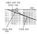
예를 들어, (0001)Si면, (000-1)C면으로부터 오프각이 8°가 되도록 기울인 SiC 단결정 기판에서, 기판 표면에서의 기저면 전위밀도는, 결정품질에도 의존하지 만, 전형적으로는 102∼104개/cm2이 된다. 도 1에 모식적으로 도시한 바와 같이, 기판(1)의 표면이 기저면 전위(3) 중, 수 % 정도가 에피택셜 성장시에 에피택셜 층(2)에 기저면 전위(3)로서 그대로 전파되고, 남은 것은 쓰레딩 에지(threading edge) 전위(4)로 변환되어 에피택셜 층(2)에 전파된다. 또한, 동일 도면에서 5는 (0001)Si면, θ는 오프각이다.For example, in a SiC single crystal substrate inclined to have an off angle of 8 ° from the (0001) Si plane and the (000-1) C plane, the base surface potential density at the substrate surface also depends on the crystal quality, but is typically 10,2-10 is a4 / cm2. As schematically shown in FIG. 1, the surface of the
이와 같이 하여 수득된 에피택셜 막이 부착된 SiC 기판을 이용하여 바이폴라 소자를 제작한 경우, 통전 시에 기저면 전위가 적층 결함으로 변환되는 영역은, 통전 시에 전자와 정공이 재결합을 일으키는 영역이다. 전자와 정공이 재결합을 일으키는 영역의 대부분은 바이폴라 소자의 드리프트 층이며, 그 일부는 드리프트 층과 주입층의 계면 부근에서 주입층 측에 관통된다. 통전에 의한 순방향 전압의 열화를 억제하기 위해서는 이들 영역에서의 기저면 전위밀도를 감소시키는 것이 효과적일 것으로 사료된다.When a bipolar device is fabricated using the SiC substrate with the epitaxial film thus obtained, the region where the base surface potential is converted into a lamination defect during energization is a region where electrons and holes recombine during energization. Most of the regions where electrons and holes cause recombination are drift layers of bipolar elements, and some of them penetrate the injection layer side near the interface between the drift layer and the injection layer. In order to suppress the degradation of the forward voltage due to the energization, it is thought that it is effective to reduce the base surface potential density in these regions.
특허문헌 1: 국제 공개 WO03/038876호 팸플릿Patent Document 1: International Publication WO03 / 038876 Pamphlet
비특허문헌 1: 「재료과학 포럼(Materials Science Forum)」, 2002년, 제 389-393권, p.1259-1264Non-Patent Document 1: Materials Science Forum, 2002, Vol. 389-393, p. 1259-1264
발명의 개시Disclosure of the Invention
발명이 해결하고자 하는 과제Problems to be Solved by the Invention
본 발명은, 상술한 종래 기술에서의 문제점을 해결하기 위하여 실시된 것이며, SiC 단결정 기판으로부터 에피택셜 층으로의 기저면 전위의 전파를 감소하고, 이에 따라 경시에서의 순방향 전압 열화(劣化)를 억제한 바이폴라형 반도체 장치 및 그의 제조방법을 제공하는 것을 목적으로 한다.The present invention has been made to solve the above-described problems in the prior art, and reduces propagation of the base surface potential from the SiC single crystal substrate to the epitaxial layer, thereby suppressing forward voltage degradation over time. An object of the present invention is to provide a bipolar semiconductor device and a manufacturing method thereof.
과제를 해결하기 위한 수단Means to solve the problem
본 발명자는 SiC 단결정 기판상에 SiC를 에피택셜 성장시키기 전에, 기판 표면에 소정의 조건으로 수소 에칭 처리를 실시함으로써, 이 처리면으로부터 성장시킨 에피택셜 막 중의 기저면 전위가 큰 폭으로 줄어듬을 확인하여 본 발명을 완성하기에 이르렀다.MEANS TO SOLVE THE PROBLEM This inventor confirmed that the base surface potential in the epitaxial film grown from this process surface is largely reduced by performing a hydrogen etching process on predetermined surface conditions before epitaxially growing SiC on a SiC single crystal substrate. The present invention has been completed.
또한, 기판 표면을 화학기계 연마로 처리하고, 이어서 수소 에칭 처리를 실시함으로써, 특히, 낮은 오프각의 기판을 이용하여 이 처리면으로부터 성장시킨 에피택셜 막 중의 기저면 전위가 매우 적게 됨을 확인하여 본 발명을 완성하기에 이르렀다.In addition, the substrate surface was treated by chemical mechanical polishing, followed by hydrogen etching, and in particular, it was confirmed that the base surface potential in the epitaxial film grown from this treatment surface using a substrate having a low off angle was very small. Came to complete.
특히, 상기 처리에 의해 표면 거칠기 Rms를 0.1∼0.6nm로 한 기판 표면으로부터 에피택셜 성장시킨 것에서는 기저면 전위가 매우 작다.Particularly, in the case where epitaxial growth is made from the surface of the substrate having the surface roughness Rms of 0.1 to 0.6 nm by the above treatment, the base surface potential is very small.
본 발명의 바이폴라형 반도체 장치는 통전 시에 전자와 정공이 재결합하는 영역의 적어도 일부를, 탄화규소 기판의 표면으로부터 성장시킨 탄화규소 에피택셜 층에 의해 형성한 바이폴라형 반도체 장치에 있어서,The bipolar semiconductor device of the present invention is a bipolar semiconductor device in which at least a part of a region where electrons and holes recombine at the time of energization is formed by a silicon carbide epitaxial layer grown from the surface of a silicon carbide substrate.
상기 탄화규소 기판에 있어서, 에피택셜 성장시키는 표면의 표면 거칠기 Rms가 0.1∼0.6nm인 것을 특징으로 한다.In the silicon carbide substrate, the surface roughness Rms of the surface to be epitaxially grown is 0.1 to 0.6 nm.
본 발명의 바이폴라형 반도체 장치는 상기 탄화규소 기판의 오프각도가 1∼4°인 것을 특징으로 한다.The bipolar semiconductor device of the present invention is characterized in that the off-angle of the silicon carbide substrate is 1 to 4 degrees.
본 발명의 바이폴라형 반도체 장치는 상기 탄화규소 기판에서의 에피택셜 성장시키는 결정면이 (000-1)C면이며, 오프각이 1∼8°인 것을 특징으로 한다.The bipolar semiconductor device of the present invention is characterized in that the crystal plane to be epitaxially grown on the silicon carbide substrate is the (000-1) C plane, and the off angle is 1 to 8 °.
본 발명의 바이폴라형 반도체 장치의 제조방법은 통전 시에 전자와 정공이 재결합하는 영역의 적어도 일부를, 탄화규소 기판의 표면으로부터 성장시킨 탄화규소 에피택셜 층에 의해 형성한 바이폴라형 반도체 장치의 제조방법에 있어서,In the method for manufacturing a bipolar semiconductor device of the present invention, a method for manufacturing a bipolar semiconductor device in which at least part of a region where electrons and holes are recombined at the time of energization is formed by a silicon carbide epitaxial layer grown from the surface of a silicon carbide substrate. To
탄화규소 기판의 표면을 수소 에칭으로 처리한 후에, 이 처리면으로부터 탄화규소를 에피택셜 성장시킴으로써 상기 에피택셜 층을 형성하는 것을 특징으로 한다.After the surface of the silicon carbide substrate is treated by hydrogen etching, the epitaxial layer is formed by epitaxially growing silicon carbide from the treated surface.
본 발명의 바이폴라형 반도체 장치의 제조방법은 통전 시에 전자와 정공이 재결합하는 영역의 적어도 일부를, 탄화규소 기판의 표면으로부터 성장시킨 탄화규소 에피택셜 층에 의해 형성한 바이폴라형 반도체 장치의 제조방법에 있어서,In the method for manufacturing a bipolar semiconductor device of the present invention, a method for manufacturing a bipolar semiconductor device in which at least part of a region where electrons and holes are recombined at the time of energization is formed by a silicon carbide epitaxial layer grown from the surface of a silicon carbide substrate. To
탄화규소 기판의 표면을 화학기계 연마로 처리하고, 이어 수소 에칭으로 처리한 후에, 이 처리면으로부터 탄화규소를 에피택셜 성장시킴으로써 상기 에피택셜 층을 형성하는 것을 특징으로 한다.The surface of the silicon carbide substrate is subjected to chemical mechanical polishing followed by hydrogen etching, and then the epitaxial layer is formed by epitaxially growing silicon carbide from the treated surface.
본 발명의 바이폴라형 반도체 장치의 제조방법은, 오프각이 1∼4°인 탄화규소 기판의 표면으로부터 에피택셜 성장시키는 것을 특징으로 한다.A method for producing a bipolar semiconductor device of the present invention is characterized by epitaxial growth from the surface of a silicon carbide substrate having an off angle of 1 to 4 degrees.
본 발명의 바이폴라형 반도체 장치의 제조방법은, 오프각이 1∼8°인 탄화규소 기판의 (000-1)C면으로부터 에피택셜 성장시키는 것을 특징으로 한다.A method for producing a bipolar semiconductor device of the present invention is characterized by epitaxial growth from a (000-1) C plane of a silicon carbide substrate having an off angle of 1 to 8 degrees.
발명의 효과Effects of the Invention
본 발명의 바이폴라형 반도체 장치는 에피택셜 층에서의 기저면 전위가 매우 작다.The bipolar semiconductor device of the present invention has a very low base surface potential in the epitaxial layer.
본 발명의 바이폴라형 반도체 장치의 제조방법에 의하면, SiC 단결정 기판으로부터 에피택셜 층으로의 기저면 전위의 전파를 큰 폭으로 저감할 수 있다.According to the bipolar semiconductor device manufacturing method of the present invention, propagation of the base surface potential from the SiC single crystal substrate to the epitaxial layer can be greatly reduced.
도 1은 기저면 전위가 SiC 단결정 기판으로부터 에피택셜 층으로 전파하는 모습을 설명하는 도면이다.BRIEF DESCRIPTION OF THE DRAWINGS It is a figure explaining the state which a base surface electric potential propagates from an SiC single crystal substrate to an epitaxial layer.
도 2는 CMP 장치의 개략적인 구성도이다.2 is a schematic configuration diagram of a CMP apparatus.
도 3은 본 실시예의 방법으로 기판 표면을 처리한 에피택셜 막이 부착된 SiC 기판을 이용하여 형성한 pn 다이오드의 일례를 도시한 단면도이다.3 is a cross-sectional view showing an example of a pn diode formed using a SiC substrate with an epitaxial film treated with a surface of the substrate by the method of this embodiment.
도 4는 실시예 및 비교예의 에피택셜 막에서의 기저면 전위밀도의 측정 결과를 나타낸 그래프이다.4 is a graph showing measurement results of base surface potential densities in epitaxial films of Examples and Comparative Examples.
도 5는 본 발명에 있어서, 에피택셜 막으로의 기저면 전위가 억제되는 구성을 설명하는 도면이다.FIG. 5 is a view for explaining a configuration in which the base surface potential to the epitaxial film is suppressed in the present invention.
<부호의 설명><Description of the code>
1SiC 단결정 기판1 SiC Single Crystal Substrate
2SiC 에피택셜 층2 SiC epitaxial layer
3기저면 전위3 base dislocation
4쓰레딩 에지 전위4 threading edge potential
5결정면5 crystal face
11연마 헤드11 polishing heads
12턴 테이블12 turn table
13연마 패드13 polishing pads
14기판14 boards
15슬러리 공급 노즐15 slurry feed nozzle
21기판21 boards
23드리프트 층23 drift floor
24p형 접합층24 p-type bonding layer
25p+형 컨택층25 p + type contact layer
26JTE26 JTE
27산화막27 oxide film
28캐소드 전극28 cathode electrode
29애노드 전극29 anode electrode
29a티탄막29a titanium film
29b알루미늄막29b aluminum film
41기저면 전위41 Base Dislocation
41a거울상 전위41a mirror image potential
42원자 스텝42 atomic steps
43번칭 스텝(bunching step)43 Bunching Step
d기저면 전위와 표면과의 거리d Base potential and surface distance
θ오프각θ off angle
발명을 실시하기To practice the invention 위한 for최량의Best 형태 shape
이하, 본 발명의 실시태양에 대하여 설명한다. 또한, 격자방위 및 격자면에 대하여, 개별 방위는 [], 개별 면은 ()로 표시하고, 음의 지수에 대해서는 결정학상, "-"(바)를 숫자 위에 붙이게 되어 있지만 명세서 작성 사정상 숫자 앞에 부호를 붙이는 것으로 한다.EMBODIMENT OF THE INVENTION Hereinafter, embodiment of this invention is described. In addition, for lattice azimuth and lattice planes, the individual orientations are indicated by [] and the individual planes are indicated by (). For negative exponents, "-" (bars) are placed on the numbers for the negative exponent. It is assumed to attach a sign.
SiC 단결정 기판으로서는 승화법 또는 CVD법에 따라 수득된 벌크 결정을 슬라이스한 것을 사용한다. 승화법(개량 Lely법)에 의한 경우, 예를 들어, 도가니에 SiC 분말을 넣고 2200∼2400℃로 가열하여 기화하고, 씨드 결정의 표면에 전형적으로는 0.8∼1mm/h의 속도로 증착하여 벌크 성장시킨다. 수득된 인고트를 소정의 두께로, 원하는 결정면이 표출하도록 슬라이스하고, 그 표면을, 예를 들어 SiC와 동등 또는 그보다도 단단한 연마지립을 이용하여 연마를 진행함과 함께, 거친 연마지립으로부터 미세한 지립으로 바꿔가면서 연마처리하여 거울면 형태로 평활화한다.As the SiC single crystal substrate, one obtained by slicing a bulk crystal obtained by the sublimation method or the CVD method is used. In the case of the sublimation method (improved Lely method), for example, SiC powder is placed in a crucible, heated to 2200-2400 ° C., vaporized, and deposited on the surface of the seed crystal at a rate of 0.8-1 mm / h, typically, in bulk. To grow. The obtained ingot is sliced to a desired thickness to exhibit a desired crystal surface, and the surface thereof is polished using, for example, abrasive grains equivalent to or harder than SiC, and fine grains from rough abrasive grains. Abrasive treatment is carried out while changing to smoothing in mirror form.
SiC 단결정의 결정형으로서는 예를 들어, 4H-SiC, 3C-SiC, 2H-SiC, 6H-SiC, 15R-SiC 등을 들 수 있지만, 절연파괴 강도 및 이동도가 높고, 이방성이 비교적 작은 4H-SiC가 바람직하게 이용되고, 후술하는 수소 에칭 처리, 또는 화학기계 연마처리와 수소 에칭 처리와의 병용에 의해 에피택셜 층 중의 기저면 전위밀도가 큰 폭으로 감소한다.As the crystalline form of the SiC single crystal, for example, 4H-SiC, 3C-SiC, 2H-SiC, 6H-SiC, 15R-SiC and the like, but 4H-SiC having high dielectric breakdown strength and mobility and relatively low anisotropy Is preferably used, and the base dislocation density in the epitaxial layer is greatly reduced by the hydrogen etching treatment described later, or in combination with the chemical mechanical polishing treatment and the hydrogen etching treatment.
에피택셜 성장을 수행하는 결정면으로서는, 예를 들어, (0001)Si면, (000-1)C면, (11-20)면, (01-10)면, (03-38)면 등을 들 수 있다. (0001)Si면, (000-1)C면에서 에피택셜 성장시키는 경우, [01-10] 방향, [11-20] 방향, 또는 [01-10] 방향과 [11-20] 방향과의 중간 방향의 오프 방위에 1∼12°, 바람직하게는 1∼8°, 특히 바람직하게는 1∼4°의 오프각으로 경사시켜 슬라이스한 기판을 사용하고, 이 결정면으로부터 스텝 플로 성장 기술에 의해 에피택셜 성장시킨다.Examples of the crystal plane for epitaxial growth include (0001) Si plane, (000-1) C plane, (11-20) plane, (01-10) plane, and (03-38) plane. Can be. When epitaxially growing on the (0001) Si plane and the (000-1) C plane, the [01-10] direction, the [11-20] direction, or the [01-10] direction and the [11-20] direction Using a substrate sliced at an off angle of 1 to 12 °, preferably 1 to 8 °, and particularly preferably 1 to 4 ° to an off direction in the intermediate direction, the substrate is epitaxially prepared by the step flow growth technique. Grows tactical.
1∼4°와 같은 낮은 오프각으로 슬라이스한 기판을 이용한 경우, 기판으로부터 에피택셜 층으로의 기저면 전위의 전파가 매우 적게 된다. 또한, 기판에서의 에피택셜 성장시키는 결정면을 (000-1)C면으로 한 경우에는, 이보다도 비교적 큰 오프각이어도 에피택셜 층으로의 기저면 전위의 전파가 적게 되며, 구체적으로는 오프각이 1∼8°인 범위 내에 있어서 기판으로부터 에피택셜 층으로의 기저면 전위의 전파가 매우 적게 된다.When a substrate sliced at a low off angle such as 1 to 4 ° is used, propagation of the base surface potential from the substrate to the epitaxial layer is very small. In the case where the crystal plane to be epitaxially grown on the substrate is a (000-1) C plane, even if the angle is relatively larger than that, the propagation of the base surface potential to the epitaxial layer is reduced, specifically, the off angle is 1. Within the range of 8 °, propagation of the base surface potential from the substrate to the epitaxial layer becomes very small.
상기 SiC 단결정 기판의 표면을 수소 에칭으로 처리한다. 수소 에칭은 예를 들어, 에피택셜 성장을 수행하는 반응로 내에서 수행할 수 있다. 반응로 내에 기판을 도입한 후, 1∼100L/min, 바람직하게는 5∼20L/min으로 수소가스 또는 염화수소를 첨가한 수소가스를 반응로 내에 도입하고, 10∼250Torr, 바람직하게는 20∼50Torr의 가스 분위기 하에서, 1300∼1700℃, 바람직하게는 1350∼1450℃의 온도로 10∼60분 정도 처리한다.The surface of the SiC single crystal substrate is treated by hydrogen etching. Hydrogen etching can be performed, for example, in a reactor that performs epitaxial growth. After introducing the substrate into the reactor, hydrogen gas or hydrogen gas added with hydrogen gas or hydrogen chloride at 1 to 100 L / min, preferably 5 to 20 L / min, is introduced into the reactor, and 10 to 250 Torr, preferably 20 to 50 Torr. Under a gas atmosphere of 1300 to 1700 ° C, preferably at a temperature of 1350 to 1450 ° C for 10 to 60 minutes.
또한, 수소와 기판표면과의 상호작용시에서의 Si의 방출속도는 주로 증발속 도로 결정되고, C의 방출속도는 주로 수소와의 반응속도로 결정되지만, Si와 C의 방출속도가 거의 동일하게 되도록 하는 온도와 압력으로 에칭 처리함으로써 이 기판 표면으로부터 성장시키는 SiC 에피택셜 층의 기저면 전위밀도가 매우 적게 된다. 상기의 수소 에칭 처리 전에, 화학기계 연마(CMP: Chemical Mechanical Polishing)에 의해 기판 표면을 처리하면, 에피택셜 층의 기저면 전위밀도가 매우 작게 된다. 도 2에 일반적인 CMP 장치의 개략 구성을 도시한다. SiC 단결정 기판(14)은 연마 헤드(11)에 고정되고, 턴 테이블(12) 위의 연마 패드(13)에 SiC 단결정 기판(14)을 가압하여 압착한 상태에서, 슬러리 공급 노즐(15)로부터 연마 슬러리를 적하하면서 연마 패드(13)와 SiC 단결정 기판(14)의 어느 한쪽 또는 양쪽을 회전 모터에 의해 회전시켜, 화학적 및 기계적 작용에 의해 연마한다. 연마 슬러리는 통상, 용매, 지립 및 첨가제로 이루어지고, 예를 들어, 콜로이드 실리카와 같은 실리카계 미립자 등을 지립으로 하여 물에 분산시킴과 동시에 필요한 첨가제를 가하고 pH를 조정한 것 등이 사용된다.In addition, the release rate of Si in the interaction between hydrogen and the substrate surface is mainly determined by the evaporation rate, and the release rate of C is mainly determined by the reaction rate with hydrogen, but the release rate of Si and C is about the same. Etching treatment at a temperature and pressure as low as possible results in very low base surface potential density of the SiC epitaxial layer grown from the substrate surface. If the substrate surface is treated by Chemical Mechanical Polishing (CMP) before the above hydrogen etching treatment, the base surface potential density of the epitaxial layer becomes very small. 2 shows a schematic configuration of a general CMP apparatus. The SiC
기판 표면을 상기 방법으로 처리한 후, 이 처리면에 CVD법을 이용하여 SiC를 에피택셜 성장시킨다. 원료가스로서, C의 원료가스인 프로판과, Si의 원료가스인 실란을 이용한다. 또한, 캐리어 가스로서 수소를, 도펀트 가스로서 질소 또는 트리메틸알루미늄 등을 이용한다. 이들 가스 분위기 하에서, 예를 들어, 1500∼1600℃, 40∼80Torr의 조건에서, 2∼20㎛/h의 성장속도로 SiC를 에피택셜 성장시킨다. 이에 따라, 기판과 동일한 결정형의 SiC가 스텝 플로 성장한다.After the substrate surface is treated by the above method, SiC is epitaxially grown on the treated surface by the CVD method. As the source gas, propane which is a source gas of C and silane which is a source gas of Si are used. In addition, hydrogen is used as a carrier gas and nitrogen, trimethylaluminum, etc. are used as a dopant gas. Under these gas atmospheres, for example, SiC is epitaxially grown at a growth rate of 2 to 20 µm / h under conditions of 1500 to 1600 ° C and 40 to 80 Torr. Thereby, SiC of the same crystalline form as a board | substrate grows step-flow.
에피택셜 성장을 수행하기 위한 구체적인 장치로서는, 수직형 핫 월 반응기 를 이용할 수 있다. 수직형 핫 월 반응기에는, 석영으로 형성된 수냉 2중 원통관이 설치되고, 수냉 2중 원통관의 내부에는 원통형 단열재, 흑연으로 형성된 핫 월 및 SiC 단결정 기판을 수직 방향으로 지지하기 위한 쐐기형 서셉터가 설치되어 있다. 수냉 2중 원통관의 외측 주위에는 고주파 가열 코일이 설치되고, 고주파 가열 코일에 의해 핫 월을 고주파 유도 가열하고, 핫 월로부터의 복사열에 의해 쐐기형 서셉터에 지지된 SiC 단결정 기판을 가열한다. SiC 단결정 기판을 가열하면서 수냉 2중 원통관의 하방으로부터 반응 가스를 공급함에 따라 SiC 단결정 기판의 표면에 SiC가 에피택셜 성장한다.As a specific apparatus for performing epitaxial growth, a vertical hot wall reactor can be used. In the vertical hot wall reactor, a water-cooled double-cylinder tube made of quartz is provided, and inside the water-cooled double-cylinder tube, a wedge-type susceptor for vertically supporting a cylindrical insulator, a hot wall made of graphite, and a SiC single crystal substrate in a vertical direction. Is installed. A high frequency heating coil is provided around the outer side of the water-cooled double cylinder tube, and the high frequency induction heating is performed by the high frequency heating coil, and the SiC single crystal substrate supported by the wedge susceptor is heated by radiant heat from the hot wall. SiC is epitaxially grown on the surface of the SiC single crystal substrate as the reaction gas is supplied from below the water-cooled double cylinder tube while the SiC single crystal substrate is heated.
이와 같이 수득된 에피택셜 막 부착 SiC를 이용하여, 바이폴라 소자를 제작한다. 바이폴라 소자로서는 예를 들어, pn 다이오드, 바이폴라 접합 트랜지스터(BJT), 사이리스터, GTO 사이리스터, IGBT 등을 들 수 있다.A bipolar element is produced using the SiC with epitaxial film thus obtained. As a bipolar element, a pn diode, a bipolar junction transistor (BJT), a thyristor, GTO thyristor, IGBT etc. are mentioned, for example.
이들 바이폴라 소자에 있어서, 통전 시에 전자와 정공이 재결합을 일으키는 영역, 예를 들어 드리프트 층 또는 드리프트 층과 주입층의 계면 부근에서의 주입층을, 상기 에피택셜 층에서 형성한다. 본 실시태양에서는, 기판에 상술한 처리를 실시한 것을 이용하므로, 에피택셜 층의 기저면 전위밀도가 매우 작다. 이 때문에, 통전 시로 인해 기저면 전위로부터 변환되는 적층 결함의 발생이 억제되고, 경시에 의한 순방향 전압 열화가 개선된다. 특히, 상술한 처리에 의해 표면 거칠기 Rms를 0.1∼0.6nm, 바람직하게는 0.1∼0.3nm로 한 기판 표면으로부터 에피택셜 성장시킨 것에서는 기저면 전위가 매우 작다.In these bipolar elements, an injection layer in the region where electrons and holes recombine during energization, for example, in the vicinity of an interface between the drift layer or the drift layer and the injection layer, is formed in the epitaxial layer. In this embodiment, since the substrate having been subjected to the above-described treatment is used, the base surface dislocation density of the epitaxial layer is very small. For this reason, generation | occurrence | production of the lamination | stacking defect converted from a base surface potential by the time of energization is suppressed, and the forward voltage deterioration with time is improved. Particularly, when epitaxially grown from the surface of the substrate having the surface roughness Rms of 0.1 to 0.6 nm, preferably 0.1 to 0.3 nm by the above-described treatment, the base surface potential is very small.
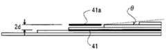
본 발명에 있어서 에피택셜 층으로의 기저면 전위의 전파가 큰 폭으로 감소 하는 것은 하기 이유에 의한 것으로 사료된다. 또한, 이하에 설명하는 구성은 어디까지나 고찰이며, 본 발명이 하기 구성에 한정하여 해석되는 것을 의도하는 것은 아니다.It is considered that the propagation of the base surface potential to the epitaxial layer is greatly reduced in the present invention due to the following reason. In addition, the structure demonstrated below is only a consideration, and it does not intend that this invention is limited to the following structure.
이하, 도 5를 참조하면서 설명한다. 일반적으로, 결정 내에 존재하는 전위에는 결정 표면과의 사이에 거울상 힘(imaging force)이 작용한다. 이 거울상 힘은 거울상 전위를 고려함으로써 산출할 수 있다. 결정표면으로부터 거리 r의 위치에, 절대값 b의 버거스(Burgers) 벡터를 갖는 전위가 존재할 때, 이 전위와 거울상 관계에 있는 전위가 갖는 힘(거울상 힘)은,A description with reference to FIG. 5 is as follows. In general, an imaging force acts on the potential present in the crystal between the crystal surface. This mirror image force can be calculated by considering the mirror image potential. When a potential having a Burgers vector of absolute value b exists at a position r from the crystal surface, the force (mirror force) of the potential in the mirror image relationship with the potential is
[수학식 1][Equation 1]

으로 표시된다(도 5(a)).It is indicated by (Fig. 5 (a)).
상기 식으로부터 알 수 있듯이, 결정 표면으로부터 전위까지의 거리 d가 가깝게 될수록 거울상 힘은 크게 된다. 또한, 이 거울상 힘의 값이 음인 것은 전위와 표면과의 사이에 인력이 작용함을 나타내고 있다. 즉, 도 5(b)에 표시한 바와 같이, SiC 단결정 중에 존재하는 기저면 전위에는 기저면 전위가 표면에 가깝게 가면, 점차 표면에 대하여 수직이 되려고 하는 인력이 작용하게 된다.As can be seen from the above equation, the closer the distance d from the crystal surface to the dislocation becomes, the larger the mirror image force becomes. In addition, the negative value of this mirror image force indicates that attractive force acts between the dislocation and the surface. That is, as shown in Fig. 5 (b), when the base surface potential is close to the surface, the attraction force that tries to be perpendicular to the surface gradually acts on the base surface potential present in the SiC single crystal.
상기 인력이 어느 임계치를 넘으면, 기저면 전위는 표면에 거의 수직인 방향(C축에 평행한 방향)으로 전파하는 쓰레딩 에지 전위로 변환되게 된다.If the attractive force exceeds a certain threshold, the base surface potential is converted into a threading edge potential that propagates in a direction almost perpendicular to the surface (direction parallel to the C axis).
SiC 단결정 기판의 (0001)Si면상 또는 (000-1)C면상으로 에피택셜 성장시키 는 경우에는 C축으로부터 약간의 각도를 기울인 결정면이 사용된다. 이로 인해, 에피택셜 막 표면은 원자 레벨에서는 계단 형태의 표면(원자 스텝)을 갖고 있다. 도 5(c)에 도시한 바와 같이, 각각의 원자 스텝(42)이 개별적으로 흩어진 상태인 이상적인 평탄 표면의 경우, 에피택셜 막의 표면과 에피택셜 막의 내부에 존재하는 기저면 전위(41)의 거리 d는 최소가 되며, 기저면 전위(41)가 표면으로부터 받는 거울상 힘(인력)이 최대가 된다. 이 때문에, 기저면 전위(41)는 결정 표면에 거의 수직하는 방향(C축 방향)으로 방향을 바꾸면서(즉, 쓰레딩 에지 전위로 변환되고) 에피택셜 단결정 막의 내부를 전파한다.In the case of epitaxial growth on the (0001) Si plane or (000-1) C plane of a SiC single crystal substrate, a crystal plane inclined at a slight angle from the C axis is used. For this reason, the epitaxial film surface has a step-shaped surface (atomic step) at the atomic level. As shown in Fig. 5C, in the case of an ideal flat surface in which each
그러나, 실제의 결정 표면에서는, 도 5(d)에 도시한 바와 같이, 결정 표면에 있어서 수개의 원자 스텝이 다발로 된 번칭 스텝(bunching step, 43)이 존재하고 있다. 이와 같이 스텝 번칭이 있는 상태에서는, 기저면 전위(41)가 표면으로부터 받는 거울상 힘(인력)이 작게 된다. 이 때문에, 기저면 전위(41)는 결정 표면에 거의 수직인 방향(C축 방향)으로 방향을 바꾸지 않고, 결정 표면과 거의 평행한 방향을 향한 채 기저면 전위(41)로서 에피택셜 단결정 막의 내부를 전파한다.However, on the actual crystal surface, as shown in Fig. 5 (d), there is a bunching
에피택셜 성장시에 있어서 SiC 단결정 기판의 결정 표면의 원자 스텝의 상태는, SiC 단결정 기판에 대한 표면 처리에 따라 변화한다. 기판 표면에 적절한 수소 에칭 처리, 또는 화학기계 연마와 수소 에칭을 병용한 처리를 실시함에 따라, 기판 표면의 원자 스텝의 번칭이 억제된다. 결정 표면에서의 원자 스텝의 번칭의 유무나 번칭 단차의 대소는 거시적으로는 표면 거칠기 Rms로 측정할 수 있으며, 에피택셜 막을 성막하기 전에 이들의 표면 처리를 실시함에 따라, 표면 거칠기 Rms가 저감된다.At the time of epitaxial growth, the state of the atomic step of the crystal surface of the SiC single crystal substrate changes with the surface treatment on the SiC single crystal substrate. By performing an appropriate hydrogen etching treatment on the substrate surface or a combination of chemical mechanical polishing and hydrogen etching, bunching of atomic steps on the substrate surface is suppressed. The presence or absence of bunching of atomic steps on the crystal surface and the magnitude of the bunching step can be measured macroscopically by surface roughness Rms, and the surface roughness Rms is reduced by performing these surface treatments before forming the epitaxial film.
수소 에칭 등의 표면 처리에 따라 결정 표면의 표면 거칠기 Rms가 어느 값 이하로 된 경우에, 기저면 전위에 작용하는 거울상 힘이 임계치를 넘어 쓰레딩 에지 전위로 변환되는 기저면 전위의 비율이 대폭으로 증대한다고 사료된다.When the surface roughness Rms of the crystal surface becomes lower than a certain value according to the surface treatment such as hydrogen etching, the ratio of the base surface potential that the mirror image force acting on the base surface potential exceeds the threshold and is converted to the threading edge potential significantly increases. do.
이상의 구성에 따라, 표면 거칠기 Rms를 0.6nm 이하, 특히 0.3nm 이하로 한 기판 표면으로부터 에피택셜 성장시킨 경우에는 기판으로부터 에피택셜 막으로의 기저면 전위의 전파가 임계적으로 작게 된다고 사료된다.According to the above structure, when epitaxially growing from the surface of the substrate whose surface roughness Rms is 0.6 nm or less, especially 0.3 nm or less, it is considered that propagation of the base surface potential from the substrate to the epitaxial film becomes critically small.
또한, 기판 표면에 다수의 결정 불완전성이 존재하는 것과 같은 경우에는, 기판으로부터 에피택셜 막으로 전파하는 에피택셜 성장시에 새로 기저면 전위가 생성되어 버리는 경우가 있다. 이 경우, 에피택셜 막 중의 기저면 전위의 밀도는 기판으로부터 에피택셜 막으로 전파한 것과, 에피택셜 성장시에 새로 생성된 것의 합산이 된다.In addition, in the case where a large number of crystal imperfections exist on the surface of the substrate, the base surface potential may be newly generated during epitaxial growth propagating from the substrate to the epitaxial film. In this case, the density of the base surface potential in the epitaxial film is the sum of the propagation from the substrate to the epitaxial film and the newly generated one at the time of epitaxial growth.
기판 표면 부분의 결정 불완전성은 적절한 조건에서 화학기계 연마나 수소 에칭 처리를 수행하여, 기판 표면을 평탄화함으로써 제거할 수 있다. 즉, 화학기계 연마나 수소 에칭 처리를 수행하여 기판 표면의 표면 거칠기를 작게 함으로써, 에피택셜 성장시에 생성되는 기저면 전위의 밀도를 저감할 수 있다. 이와 같이, 표면 거칠기 Rms를 0.6nm 이하, 특히 0.3nm 이하로 한 기판 표면으로부터 에피택셜 성장시킨 경우에는 기판으로부터 에피택셜 막으로의 기저면 전위의 전파가 임계적으로 작게 됨과 동시에, 에피택셜 성장시에 새로 생성되는 기저면 전위의 밀도도 감소되어, 결과로 기저면 전위 밀도가 매우 작은 에피택셜 막을 얻을 수 있다고 사 료된다.Crystalline imperfections in the substrate surface portion can be removed by performing chemical mechanical polishing or hydrogen etching treatment under appropriate conditions to planarize the substrate surface. In other words, by performing chemical mechanical polishing or hydrogen etching treatment to reduce the surface roughness of the substrate surface, the density of the base surface potential generated during epitaxial growth can be reduced. As described above, when epitaxial growth is made from the surface of the substrate having the surface roughness Rms of 0.6 nm or less, particularly 0.3 nm or less, the propagation of the base surface potential from the substrate to the epitaxial film becomes critically small, and at the time of epitaxial growth. The density of newly generated basal dislocations is also reduced, resulting in epitaxial films with very small basal dislocation densities.
또한, 도 5(e)에 도시한 바와 같이, 오프각 θ가 작을수록 기저면 전위(41)는 결합 표면에 근접하기 때문에, 오프각 θ가 작게 되면 기저면 전위(41)에 작용하는 단위 길이당 거울상 힘이 크게 된다. 즉, 오프각 θ가 작을수록 에피택셜 성장시에 스레딩 전위로 변환되는 기저면 전위의 비율이 증대한다.In addition, as shown in Fig. 5E, the smaller the off angle θ is, the closer the
SiC 단결정 기판의 (0001)Si면상 또는 (000-1)C면상의 에피택셜 성장은, 오프각도가 너무 작게 되면 곤란하기 때문에 실용적으로는 1° 이상의 오프각도가 필요하게 된다. 이상의 점에서, 1∼12°, 바람직하게는 1∼8°, 보다 바람직하게는 1∼4°의 오프각도로 슬라이스한 기판을 이용한 경우에, 기판으로부터의 기저면 전위의 전파가 작은 양질의 에피택셜 층이 수득된다.Epitaxial growth on the (0001) Si plane or on the (000-1) C plane of the SiC single crystal substrate is difficult when the off angle is too small, so that an off angle of 1 ° or more is practically required. In view of the above, in the case of using a substrate sliced at an off angle of 1 to 12 degrees, preferably 1 to 8 degrees, and more preferably 1 to 4 degrees, high-quality epitaxial that small propagation of the base surface potential from the substrate is small. A layer is obtained.
또한, (0001)Si면과 (000-1)C면을 비교한 경우에는, (000-1)C면의 쪽이 스텝 번칭을 일으키기 어려운 성질을 갖고 있기 때문에, (000-1)C면의 경우에는 1∼8°의 오프각도이어도 기저면 전위의 밀도가 매우 작은 에피택셜 층을 얻을 수 있다.In the case where the (0001) Si plane and the (000-1) C plane are compared, the (000-1) C plane has a property of hardly causing step bunching. In this case, even at an off angle of 1 to 8 °, an epitaxial layer having a very low density of the base surface potential can be obtained.
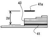
도 3은 바이폴라 소자의 하나인 pn(pin) 다이오드의 일례를 나타낸 단면도이다. Lely법에 의해 성장시킨 인고트를 소정의 오프각으로 슬라이스하고, 표면을 거울면 연마한 n형의 4H-SiC 기판을, 상기의 조건에서 수소 에칭 및 화학기계 연마로 처리한 SiC 단결정 기판(21)(캐리어 밀도 8×1018cm-3, 두께 400㎛)의 위에, CVD법에 따라 질소 도핑 n형 SiC층과 알루미늄 도핑 p형 SiC층을 순차적으로 에피택셜 성장시킨다.3 is a cross-sectional view showing an example of a pn (pin) diode which is one of bipolar devices. SiC
n형 성장층인 드리프트층(23)은 도너 밀도 5×1014cm-3, 막 두께 40㎛이다.The
p형 성장층은 p형 접합층(24)과 p+형 컨택층(25)으로 이루어진다. p형 접합층(24)은 억셉터 밀도 5×1017cm-3, 막 두께 1.5㎛이다. p+형 컨택층(25)은 억셉터 밀도 1×1018cm-3, 막 두께 0.5㎛이다.The p-type growth layer is composed of a p-
반응성 이온 에칭에 의해 에피택셜 층의 외주부를 제거하여 메사(mesa) 구조로 한 후, 메사 저부에서의 전계 집중을 완화하기 위하여, 알루미늄 이온을 주입하여 JTE(junction termination extension)(26)를 형성한다. JTE(26)는 전체 도스(dose)량 1.2×1013cm-2, 폭 250㎛, 깊이 0.7㎛이며, 30∼450keV의 사이에서 에너지를 변경하면서 실온에서 이온 주입한 후, 아르곤 가스 분위기 하에서 1700℃의 열처리를 수행하여 활성화한다. 27은 주입 이온을 활성화한 후에 형성한 열산화막이다.After removing the outer periphery of the epitaxial layer by reactive ion etching to form a mesa structure, aluminum ions are implanted to form a junction termination extension (JTE) 26 to mitigate electric field concentration at the bottom of the mesa. .
28은 SiC 단결정 기판(21)의 하면에 Ni(두께 350nm)을 증착하여 형성한 캐소드 전극, 29는 p+형 컨택층(25)의 위에, Ti(두께 350nm)와 Al(두께 100nm)의 막(29a, 29b)을 각각 증착하여 형성한 애노드 전극이다. 이들 전극은 증착 후에 1000℃에서 20분간의 열처리를 행하여 옴 전극으로 기능한다.28 is a cathode electrode formed by depositing Ni (thickness 350 nm) on the lower surface of the SiC
상기 pn 다이오드에서는 드리프트층(23)을 수소 에칭 및 화학기계 연마로 처리한 SiC 단결정 기판(21)의 표면으로부터 성장시킨 에피택셜 막으로 구성되어 있어, 드리프트층(23)에서의 기저면 전위 밀도가 작다. 이 때문에, 통전 시에 있어 서, 전자와 정공의 재결합 에너지에 의한 적층 결함으로의 변환이 억제되어 소자의 수명을 길게 할 수 있다.In the pn diode, the
이상, 본 발명의 실시태양을 설명하였지만, 본 발명은 상기 실시태양에 한정되는 것은 아니며, 본 발명의 요지를 일탈하지 않는 범위 내에서 각종의 변형, 변경이 가능하다.As mentioned above, although embodiment of this invention was described, this invention is not limited to the said embodiment, A various deformation | transformation and a change are possible in the range which does not deviate from the summary of this invention.
실시예 1:Example1 :
수직형 핫 월 반응기를 이용하여, 개량 Lely법으로 성장시킨 인고트를 오프 방향 [11-20], 오프각도 8°로 슬라이스하고, 표면을 지립에 의한 기계연마로 거울면 형태로 한 n형의 4H-SiC(0001) 기판에 대하여, 유량 10L/min으로 수소가스를 공급하면서, 온도 1400℃, 압력 30Torr로 40분간 에칭 처리하였다. 처리 후의 기판 표면의 표면 거칠기 Rms를 세이코 인스트루먼트사 제품의 원자간력 현미경 SPI3800N을 이용하여 측정한 결과, 0.25nm(10㎛×10㎛의 영역)였다.Ingots grown by the improved Lely method using a vertical hot wall reactor were sliced in an off direction [11-20] and an off angle of 8 °, and the n-type of the surface was mirror-shaped by mechanical polishing by abrasive grains. The 4H-SiC (0001) substrate was etched for 40 minutes at a temperature of 1400 占 폚 and a pressure of 30 Torr while supplying hydrogen gas at a flow rate of 10 L / min. It was 0.25 nm (region of 10 micrometers x 10 micrometers) when the surface roughness Rms of the surface of the board | substrate after a process was measured using the atomic force microscope SPI3800N by Seiko Instruments.
계속해서, 처리 후의 기판 표면에 CVD법에 의해 SiC를 에피택셜 성장시켰다. 프로판(8cc/min), 실란(30cc/min), 수소(10L/min)를 공급하면서, 온도 1545℃, 압력 42Torr에서 4시간 스텝 플로 성장시켜, 막 두께 60㎛의 에피택셜 막을 형성하였다.Subsequently, SiC was epitaxially grown on the substrate surface after the treatment by the CVD method. A stepped growth was performed for 4 hours at a temperature of 1545 ° C. and a pressure of 42 Torr while supplying propane (8 cc / min), silane (30 cc / min), and hydrogen (10 L / min) to form an epitaxial film having a thickness of 60 μm.
수득된 에피택셜 막이 부착된 SiC 단결정 기판에 대하여, 용융 KOH 에칭과 X선 토포그래프에 의해 에피택셜 막 중의 기저면 전위 밀도를 측정한 결과, 평균값 으로 440cm-2이었다.About the obtained SiC single crystal substrate with an epitaxial film | membrane, it was 440cm <-2> as an average value when the base surface dislocation density in an epitaxial film was measured by melt KOH etching and X-ray topography.
실시예 2:Example2 :
수소 에칭 처리를 수행하기 전에, 기판 표면을 화학기계 연마에 의해 처리한 점 외에는 실시예 1과 동일하게 하여 에피택셜 막이 부착된 SiC 단결정 기판을 수득하였다. 처리 후의 기판 표면의 표면 거칠기 Rms를 실시예 1과 동일한 방법으로 측정한 결과, 0.20nm(10㎛×10㎛의 영역)이었다.Prior to performing the hydrogen etching treatment, an SiC single crystal substrate with an epitaxial film was obtained in the same manner as in Example 1 except that the substrate surface was treated by chemical mechanical polishing. It was 0.20 nm (region of 10 micrometers x 10 micrometers) when the surface roughness Rms of the surface of the board | substrate after a process was measured by the method similar to Example 1.
수득된 에피택셜 막 부착 SiC 단결정 기판에 대하여, 용융 KOH 에칭과 X선 토포그래프에 의해 에피택셜 막 중의 기저면 전위밀도를 측정한 결과, 평균값으로 60cm-2이었다.About the obtained SiC single crystal substrate with an epitaxial film, the base surface potential density in an epitaxial film was measured by melt KOH etching and X-ray topography, As a result, it was 60 cm <-2> as an average value.
실시예 3:Example3 :
개량 Lely법에 의해 성장시킨 인고트를 오프방향 [11-20], 오프각도 8°로 슬라이스하고, 표면을 지립에 의한 기계연마로 거울면 형태로 한 n형의 4H-SiC(000-1) 기판을 이용하여, 실시예 2와 동일하게 화학기계 연마 처리 및 수소 에칭 처리를 수행한 후에 에피택셜 막을 성장시켰다. 또한, 처리 후의 기판 표면의 표면 거칠기 Rms를 실시예 1과 동일한 방법으로 측정한 결과, 0.20nm(10㎛×10㎛의 영역)이었다.N-type 4H-SiC (000-1) in which an ingot grown by the improved Lely method was sliced in an off direction [11-20] and an off angle of 8 °, and the surface was mirror-shaped by mechanical polishing by abrasive grains. Using the substrate, the epitaxial film was grown after performing the chemical mechanical polishing treatment and the hydrogen etching treatment in the same manner as in Example 2. Moreover, as a result of measuring the surface roughness Rms of the surface of the board | substrate after a process in the same way as Example 1, it was 0.20 nm (region of 10 micrometers x 10 micrometers).
수득된 에피택셜 막 부착 SiC 단결정 기판에 대하여, 용융 KOH 에칭과 X선 토포그래프에 의해 에피택셜 막 중의 기저면 전위밀도를 측정한 결과, 평균값으로 20cm-2이었다.About the obtained SiC single crystal substrate with an epitaxial film, the base surface potential density in an epitaxial film was measured by melt KOH etching and X-ray topography, It was 20 cm <-2> in an average value.
실시예 4:Example4 :
개량 Lely법에 의해 성장시킨 인고트를 오프방향 [11-20], 오프각도 4°로 슬라이스하고, 표면을 지립에 의한 기계연마로 거울면 형태로 한 n형의 4H-SiC(0001) 기판을 이용하여, 실시예 2와 동일하게 화학기계 연마처리 및 수소 에칭 처리를 수행한 후에 에피택셜 막을 성장시켰다. 또한, 처리 후의 기판 표면의 표면 거칠기 Rms를 실시예 1과 동일한 방법으로 측정한 결과, 0.28nm(10㎛×10㎛의 영역)이었다.An ingot grown by the improved Lely method was sliced in an off direction [11-20] and an off angle of 4 °, and an n-type 4H-SiC (0001) substrate having a surface polished by mechanical grinding by abrasive grains was formed. Using this, the epitaxial film was grown after performing chemical mechanical polishing and hydrogen etching treatment in the same manner as in Example 2. Moreover, as a result of measuring the surface roughness Rms of the surface of the board | substrate after a process in the same manner as Example 1, it was 0.28 nm (region of 10 micrometers x 10 micrometers).
수득된 에피택셜 막 부착 SiC 단결정 기판에 대하여, 용융 KOH 에칭과 X선 토포그래프에 의해 에피택셜 막 중의 기저면 전위밀도를 측정한 결과, 평균값으로 20cm-2이었다.About the obtained SiC single crystal substrate with an epitaxial film, the base surface potential density in an epitaxial film was measured by melt KOH etching and X-ray topography, It was 20 cm <-2> in an average value.
비교예 1:Comparative Example1 :
수소 에칭 처리를 수행하지 않은 점 외에는 실시예 1과 동일하게 하여 에피택셜 막 부착 SiC 단결정 기판을 얻었다. 또한, 에피택셜 성장시키는 기판 표면의 표면 거칠기 Rms를 실시예 1과 동일한 방법으로 측정한 결과, 1.0nm이었다. 수득된 에피택셜 막 부착 SiC 단결정 기판에 대하여, 용융 KOH 에칭과 X선 토포그래프 에 의해 에피택셜 막 중의 기저면 전위밀도를 측정한 결과, 1700cm-2이었다.A SiC single crystal substrate with an epitaxial film was obtained in the same manner as in Example 1 except that the hydrogen etching treatment was not performed. The surface roughness Rms of the substrate surface subjected to epitaxial growth was measured in the same manner as in Example 1, and the result was 1.0 nm. About the obtained SiC single crystal substrate with an epitaxial film | membrane, it was 1700 cm <-2> as a result of measuring the base surface dislocation density in an epitaxial film by melt KOH etching and X-ray topography.
또한, 이 에피택셜 막을 X선 토포그래프에 따라 상세하게 해석한 결과, 1700cm-2의 기저면 전위 중, 약 반수가 기판으로부터 에피택셜 막 중에 전파한 것이며, 약 반수가 에피택셜 성장 시에 생성된 것임이 판명되었다. 즉, 수소 에칭을 처리하지 않았던 경우에는, 다량의 기저면 전위가 기판으로부터 에피택셜 막에 전파할뿐만 아니라, 다량의 기저면 전위가 에피택셜 성장 시에 생성된 것으로 사료된다.In addition, as a result of analyzing the epitaxial film in detail according to the X-ray topography, about half of the 1700 cm-2 base surface potentials propagated from the substrate to the epitaxial film, and about half of them were produced during epitaxial growth. It turned out. In other words, when the hydrogen etching was not performed, it is considered that not only a large amount of base surface potential propagates from the substrate to the epitaxial film but also a large amount of base surface potential was generated during epitaxial growth.
상기 실시예 1, 2 및 비교예 1의 결과를 도 4에 나타내었다.The results of Examples 1 and 2 and Comparative Example 1 are shown in FIG. 4.
실시예 5,비교예 2:Example5,Comparative Example2 :
SiC 인고트를 슬라이스하여 수득한 n형 4H-SiC 기판의 표면을, 화학기계 연마로 처리하고, 이어 수소 에칭으로 처리한 후, CVD법에 의해 SiC를 에피택셜 성장시킨 에피택셜 막 부착 SiC 단결정 기판을 준비하였다. 이를 이용하여 도 3과 같은 pn 다이오드를 제작하여, 실시예 5의 pn 다이오드를 수득하였다.The surface of the n-type 4H-SiC substrate obtained by slicing the SiC ingot was subjected to chemical mechanical polishing, followed by hydrogen etching, and then to the SiC single crystal substrate with epitaxial film in which SiC was epitaxially grown by CVD. Was prepared. Using this to prepare a pn diode as shown in Figure 3, to obtain a pn diode of Example 5.
한편, 상기 기판의 표면에 대하여 이들 처리를 하지 않고 그대로 SiC를 에피택셜 성장시킨 에피택셜 막 부착 SiC 단결정 기판을 준비하였다. 이를 이용하여 도 3과 같은 pn 다이오드를 제작하여, 비교예 2의 pn 다이오드를 수득하였다.On the other hand, the SiC single crystal substrate with an epitaxial film which epitaxially grown SiC was prepared as it is, without performing these processes with respect to the surface of the said board | substrate. Using this to prepare a pn diode as shown in Figure 3, to obtain a pn diode of Comparative Example 2.
이들 pn 다이오드에 대하여 순방향 전압 열화의 시험을 수행한 결과, 실시예 5의 pn 다이오드에서는, 비교예 2의 pn 다이오드와 비교하여, 100A/cm-2로 1시간의 통전을 수행하였을 때의 순방향 전압의 증가가 약 1/4로 억제되었다.As a result of the test of forward voltage deterioration with respect to these pn diodes, in the pn diode of Example 5, compared with the pn diode of Comparative Example 2, forward voltage when conducting electricity for 1 hour at 100 A / cm-2 was performed. The increase of was suppressed to about 1/4.
Claims (7)
Translated fromKoreanApplications Claiming Priority (2)
| Application Number | Priority Date | Filing Date | Title |
|---|---|---|---|
| JP2004092666 | 2004-03-26 | ||
| JPJP-P-2004-00092666 | 2004-03-26 |
Publications (2)
| Publication Number | Publication Date |
|---|---|
| KR20070029694Atrue KR20070029694A (en) | 2007-03-14 |
| KR100853991B1 KR100853991B1 (en) | 2008-08-25 |
Family
ID=35056457
Family Applications (1)
| Application Number | Title | Priority Date | Filing Date |
|---|---|---|---|
| KR1020067022103AExpired - Fee RelatedKR100853991B1 (en) | 2004-03-26 | 2005-03-25 | Bipolar semiconductor device and manufacturing method thereof |
Country Status (6)
| Country | Link |
|---|---|
| US (1) | US20070290211A1 (en) |
| EP (1) | EP1739726A4 (en) |
| KR (1) | KR100853991B1 (en) |
| CN (1) | CN1938820A (en) |
| TW (1) | TW200539318A (en) |
| WO (1) | WO2005093796A1 (en) |
Families Citing this family (50)
| Publication number | Priority date | Publication date | Assignee | Title |
|---|---|---|---|---|
| JP5131675B2 (en)* | 2006-08-25 | 2013-01-30 | 国立大学法人京都大学 | Method for manufacturing silicon carbide substrate |
| JP4842094B2 (en)* | 2006-11-02 | 2011-12-21 | 新日本製鐵株式会社 | Epitaxial silicon carbide single crystal substrate manufacturing method |
| JP5147244B2 (en)* | 2007-01-17 | 2013-02-20 | 関西電力株式会社 | Bipolar semiconductor device |
| US20100224952A1 (en)* | 2007-03-26 | 2010-09-09 | Sumitomo Electric Industries, Ltd. | Schottky barrier diode and method of producing the same |
| KR101287787B1 (en) | 2007-09-12 | 2013-07-18 | 쇼와 덴코 가부시키가이샤 | EPITAXIAL SiC SINGLE CRYSTAL SUBSTRATE AND METHOD FOR MANUFACTURING EPITAXIAL SiC SINGLE CRYSTAL SUBSTRATE |
| US8652255B2 (en)* | 2007-10-12 | 2014-02-18 | The United States Of America, As Represented By The Secretary Of The Navy | Method of producing epitaxial layers with low basal plane dislocation concentrations |
| JP5504597B2 (en)* | 2007-12-11 | 2014-05-28 | 住友電気工業株式会社 | Silicon carbide semiconductor device and manufacturing method thereof |
| US20110006399A1 (en)* | 2007-12-28 | 2011-01-13 | Sumitomo Chemical Company, Limited | Semiconductor wafer and semiconductor wafer manufacturing method |
| JP5243815B2 (en)* | 2008-02-27 | 2013-07-24 | 新日本無線株式会社 | Semiconductor device |
| US8497552B2 (en) | 2008-12-01 | 2013-07-30 | Cree, Inc. | Semiconductor devices with current shifting regions and related methods |
| US8536582B2 (en)* | 2008-12-01 | 2013-09-17 | Cree, Inc. | Stable power devices on low-angle off-cut silicon carbide crystals |
| JP5436231B2 (en)* | 2009-01-16 | 2014-03-05 | 昭和電工株式会社 | Semiconductor element manufacturing method, semiconductor element, and semiconductor device |
| JP4719314B2 (en)* | 2009-01-30 | 2011-07-06 | 新日本製鐵株式会社 | Epitaxial silicon carbide single crystal substrate and manufacturing method thereof |
| WO2010090024A1 (en)* | 2009-02-04 | 2010-08-12 | 日立金属株式会社 | Silicon carbide monocrystal substrate and manufacturing method therefor |
| JP2010184833A (en)* | 2009-02-12 | 2010-08-26 | Denso Corp | Silicon carbide single crystal substrate and silicon carbide single crystal epitaxial wafer |
| US8030151B2 (en)* | 2009-03-27 | 2011-10-04 | National Semiconductor Corporation | Configuration and fabrication of semiconductor structure having bipolar junction transistor in which non-monocrystalline semiconductor spacing portion controls base-link length |
| TW201044587A (en)* | 2009-03-27 | 2010-12-16 | Sumitomo Electric Industries | Mosfet and method for manufacturing mosfet |
| US9464366B2 (en) | 2009-08-20 | 2016-10-11 | The United States Of America, As Represented By The Secretary Of The Navy | Reduction of basal plane dislocations in epitaxial SiC |
| US10256090B2 (en) | 2009-08-20 | 2019-04-09 | The United States Of America, As Represented By The Secretary Of The Navy | Reduction of basal plane dislocations in epitaxial SiC using an in-situ etch process |
| US10256094B2 (en) | 2009-08-20 | 2019-04-09 | The Government Of The United States Of America, As Represented By The Secretary Of The Navy | Reduction of basal plane dislocations in epitaxial SiC using an in-situ etch process |
| JP4959763B2 (en)* | 2009-08-28 | 2012-06-27 | 昭和電工株式会社 | SiC epitaxial wafer and manufacturing method thereof |
| CN101877309B (en)* | 2009-10-30 | 2011-09-21 | 西安电子科技大学 | Epitaxy method to improve 4H-SiC basal plane dislocation conversion rate |
| WO2011070929A1 (en) | 2009-12-11 | 2011-06-16 | Semiconductor Energy Laboratory Co., Ltd. | Semiconductor device and electronic device |
| EP3869537A1 (en)* | 2010-03-23 | 2021-08-25 | Sumitomo Electric Industries, Ltd. | Semiconductor device and method for manufacturing same |
| JP5598542B2 (en) | 2010-05-10 | 2014-10-01 | 三菱電機株式会社 | Silicon carbide epitaxial wafer and manufacturing method thereof, silicon carbide bulk substrate for epitaxial growth and manufacturing method thereof |
| US8445386B2 (en)* | 2010-05-27 | 2013-05-21 | Cree, Inc. | Smoothing method for semiconductor material and wafers produced by same |
| JP6025306B2 (en)* | 2011-05-16 | 2016-11-16 | 株式会社豊田中央研究所 | SiC single crystal, SiC wafer and semiconductor device |
| JP5961357B2 (en)* | 2011-09-09 | 2016-08-02 | 昭和電工株式会社 | SiC epitaxial wafer and manufacturing method thereof |
| US8860040B2 (en) | 2012-09-11 | 2014-10-14 | Dow Corning Corporation | High voltage power semiconductor devices on SiC |
| US9018639B2 (en) | 2012-10-26 | 2015-04-28 | Dow Corning Corporation | Flat SiC semiconductor substrate |
| US9017804B2 (en) | 2013-02-05 | 2015-04-28 | Dow Corning Corporation | Method to reduce dislocations in SiC crystal growth |
| US9797064B2 (en) | 2013-02-05 | 2017-10-24 | Dow Corning Corporation | Method for growing a SiC crystal by vapor deposition onto a seed crystal provided on a support shelf which permits thermal expansion |
| US9738991B2 (en) | 2013-02-05 | 2017-08-22 | Dow Corning Corporation | Method for growing a SiC crystal by vapor deposition onto a seed crystal provided on a supporting shelf which permits thermal expansion |
| US9994951B2 (en) | 2013-03-15 | 2018-06-12 | The United States Of America, As Represented By The Secretary Of The Navy | Photovoltaic sputtering targets fabricated from reclaimed materials |
| US8940614B2 (en) | 2013-03-15 | 2015-01-27 | Dow Corning Corporation | SiC substrate with SiC epitaxial film |
| JP2014189442A (en)* | 2013-03-27 | 2014-10-06 | Sumitomo Electric Ind Ltd | Production method of silicon carbide semiconductor substrate |
| JP6311384B2 (en) | 2014-03-24 | 2018-04-18 | 三菱電機株式会社 | Method for manufacturing silicon carbide semiconductor device |
| WO2015159949A1 (en)* | 2014-04-18 | 2015-10-22 | 国立研究開発法人産業技術総合研究所 | Epitaxial silicon carbide wafer and process for producing same |
| JP6315579B2 (en) | 2014-07-28 | 2018-04-25 | 昭和電工株式会社 | Method for manufacturing SiC epitaxial wafer |
| US9279192B2 (en) | 2014-07-29 | 2016-03-08 | Dow Corning Corporation | Method for manufacturing SiC wafer fit for integration with power device manufacturing technology |
| WO2016125404A1 (en) | 2015-02-02 | 2016-08-11 | 富士電機株式会社 | Method for manufacturing silicon carbide semiconductor device, and silicon carbide semiconductor device |
| CN104867818B (en)* | 2015-04-02 | 2017-08-25 | 中国电子科技集团公司第十三研究所 | A kind of method for reducing silicon carbide epitaxy material defect |
| CN105185820B (en)* | 2015-08-18 | 2017-12-12 | 华中科技大学 | A kind of semiconductor opening switch based on carborundum and preparation method thereof |
| CN108138360B (en)* | 2015-10-07 | 2020-12-08 | 住友电气工业株式会社 | Silicon carbide epitaxial substrate and method for manufacturing silicon carbide semiconductor device |
| DE112017003660B4 (en)* | 2016-07-21 | 2024-08-01 | Mitsubishi Electric Corp. | SILICON CARBIDE SEMICONDUCTOR UNIT AND METHOD FOR PRODUCING A SILICON CARBIDE SEMICONDUCTOR UNIT |
| CN107910360A (en)* | 2017-12-06 | 2018-04-13 | 中国工程物理研究院电子工程研究所 | A kind of novel silicon carbide small angle inclination table top terminal structure and preparation method thereof |
| JP6481790B2 (en)* | 2018-03-20 | 2019-03-13 | 昭和電工株式会社 | SiC epitaxial wafer |
| US12125881B2 (en)* | 2018-12-04 | 2024-10-22 | Sumitomo Electric Industries, Ltd. | Silicon carbide epitaxial substrate and silicon carbide semiconductor device |
| TWI854210B (en)* | 2021-04-15 | 2024-09-01 | 環球晶圓股份有限公司 | Fabrication method of semiconductor substrate |
| CN115635380B (en)* | 2022-12-26 | 2023-03-17 | 华芯半导体研究院(北京)有限公司 | Vapor phase epitaxial growth auxiliary device |
Family Cites Families (8)
| Publication number | Priority date | Publication date | Assignee | Title |
|---|---|---|---|---|
| US4684413A (en)* | 1985-10-07 | 1987-08-04 | Rca Corporation | Method for increasing the switching speed of a semiconductor device by neutron irradiation |
| JPH10261615A (en)* | 1997-03-17 | 1998-09-29 | Fuji Electric Co Ltd | Method for controlling surface morphology of SiC semiconductor and method for growing SiC semiconductor thin film |
| JP2001077030A (en)* | 1999-08-31 | 2001-03-23 | Sanyo Electric Co Ltd | Method for manufacturing silicon carbide semiconductor device |
| JP4581270B2 (en)* | 2001-03-05 | 2010-11-17 | 住友電気工業株式会社 | SiC semiconductor ion-implanted layer and method of manufacturing the same |
| EP1306890A2 (en)* | 2001-10-25 | 2003-05-02 | Matsushita Electric Industrial Co., Ltd. | Semiconductor substrate and device comprising SiC and method for fabricating the same |
| US6849874B2 (en)* | 2001-10-26 | 2005-02-01 | Cree, Inc. | Minimizing degradation of SiC bipolar semiconductor devices |
| JP3929375B2 (en)* | 2002-08-06 | 2007-06-13 | 三菱電機株式会社 | Method for evaluating semiconductor crystal substrate |
| TWI272874B (en)* | 2002-08-09 | 2007-02-01 | Semiconductor Energy Lab | Organic electroluminescent device |
- 2005
- 2005-03-25CNCNA200580009661XApatent/CN1938820A/enactivePending
- 2005-03-25USUS10/594,045patent/US20070290211A1/ennot_activeAbandoned
- 2005-03-25KRKR1020067022103Apatent/KR100853991B1/ennot_activeExpired - Fee Related
- 2005-03-25EPEP05721512Apatent/EP1739726A4/ennot_activeWithdrawn
- 2005-03-25WOPCT/JP2005/005585patent/WO2005093796A1/enactiveApplication Filing
- 2005-03-28TWTW094109526Apatent/TW200539318A/enunknown
Also Published As
| Publication number | Publication date |
|---|---|
| KR100853991B1 (en) | 2008-08-25 |
| TW200539318A (en) | 2005-12-01 |
| EP1739726A1 (en) | 2007-01-03 |
| WO2005093796A1 (en) | 2005-10-06 |
| EP1739726A4 (en) | 2009-08-26 |
| CN1938820A (en) | 2007-03-28 |
| US20070290211A1 (en) | 2007-12-20 |
Similar Documents
| Publication | Publication Date | Title |
|---|---|---|
| KR100853991B1 (en) | Bipolar semiconductor device and manufacturing method thereof | |
| JP4185215B2 (en) | SiC wafer, SiC semiconductor device, and method of manufacturing SiC wafer | |
| EP1981076B1 (en) | Method for manufacturing silicon carbide semiconductor device | |
| JP5285202B2 (en) | Bipolar semiconductor device and manufacturing method thereof | |
| EP1215730B9 (en) | SiC WAFER, SiC SEMICONDUCTOR DEVICE AND PRODUCTION METHOD OF SiC WAFER | |
| KR20120023710A (en) | Semiconductor device | |
| US20170179236A1 (en) | Method of producing silicon carbide epitaxial substrate, silicon carbide epitaxial substrate, and silicon carbide semiconductor device | |
| EP1933386B1 (en) | Process for producing silicon carbide semiconductor device | |
| KR20120022952A (en) | Silicon carbide substrate manufacturing method and silicon carbide substrate | |
| US20110284871A1 (en) | Silicon carbide substrate, semiconductor device, and method for manufacturing silicon carbide substrate | |
| JP2007131504A (en) | SiC epitaxial wafer and semiconductor device using the same | |
| US8455269B2 (en) | Method for recovering an on-state forward voltage and, shrinking stacking faults in bipolar semiconductor devices, and the bipolar semiconductor devices | |
| JP4879507B2 (en) | Bipolar semiconductor device forward voltage recovery method, stacking fault reduction method, and bipolar semiconductor device | |
| CA2753709A1 (en) | Method of manufacturing silicon carbide substrate | |
| Kojima et al. | Reducing the wafer off angle for 4H-SiC homoepitaxy | |
| WO2008015764A1 (en) | Operating method of bipolar semiconductor device and bipolar semiconductor device | |
| JP2007027630A (en) | Bipolar semiconductor device and manufacturing method thereof | |
| JP2006237125A (en) | Bipolar semiconductor device operating method and bipolar semiconductor device | |
| WO2008015765A1 (en) | Bipolar semiconductor device and process for producing the same | |
| WO2011086734A1 (en) | Process for production of silicon carbide substrate |
Legal Events
| Date | Code | Title | Description |
|---|---|---|---|
| A201 | Request for examination | ||
| PA0105 | International application | St.27 status event code:A-0-1-A10-A15-nap-PA0105 | |
| PA0201 | Request for examination | St.27 status event code:A-1-2-D10-D11-exm-PA0201 | |
| PG1501 | Laying open of application | St.27 status event code:A-1-1-Q10-Q12-nap-PG1501 | |
| E902 | Notification of reason for refusal | ||
| PE0902 | Notice of grounds for rejection | St.27 status event code:A-1-2-D10-D21-exm-PE0902 | |
| T11-X000 | Administrative time limit extension requested | St.27 status event code:U-3-3-T10-T11-oth-X000 | |
| T11-X000 | Administrative time limit extension requested | St.27 status event code:U-3-3-T10-T11-oth-X000 | |
| T11-X000 | Administrative time limit extension requested | St.27 status event code:U-3-3-T10-T11-oth-X000 | |
| P11-X000 | Amendment of application requested | St.27 status event code:A-2-2-P10-P11-nap-X000 | |
| P13-X000 | Application amended | St.27 status event code:A-2-2-P10-P13-nap-X000 | |
| E701 | Decision to grant or registration of patent right | ||
| PE0701 | Decision of registration | St.27 status event code:A-1-2-D10-D22-exm-PE0701 | |
| GRNT | Written decision to grant | ||
| PR0701 | Registration of establishment | St.27 status event code:A-2-4-F10-F11-exm-PR0701 | |
| PR1002 | Payment of registration fee | St.27 status event code:A-2-2-U10-U12-oth-PR1002 Fee payment year number:1 | |
| PG1601 | Publication of registration | St.27 status event code:A-4-4-Q10-Q13-nap-PG1601 | |
| FPAY | Annual fee payment | Payment date:20110719 Year of fee payment:4 | |
| PR1001 | Payment of annual fee | St.27 status event code:A-4-4-U10-U11-oth-PR1001 Fee payment year number:4 | |
| FPAY | Annual fee payment | Payment date:20120802 Year of fee payment:5 | |
| PR1001 | Payment of annual fee | St.27 status event code:A-4-4-U10-U11-oth-PR1001 Fee payment year number:5 | |
| PN2301 | Change of applicant | St.27 status event code:A-5-5-R10-R13-asn-PN2301 St.27 status event code:A-5-5-R10-R11-asn-PN2301 | |
| LAPS | Lapse due to unpaid annual fee | ||
| PC1903 | Unpaid annual fee | St.27 status event code:A-4-4-U10-U13-oth-PC1903 Not in force date:20130820 Payment event data comment text:Termination Category : DEFAULT_OF_REGISTRATION_FEE | |
| PC1903 | Unpaid annual fee | St.27 status event code:N-4-6-H10-H13-oth-PC1903 Ip right cessation event data comment text:Termination Category : DEFAULT_OF_REGISTRATION_FEE Not in force date:20130820 | |
| P22-X000 | Classification modified | St.27 status event code:A-4-4-P10-P22-nap-X000 | |
| P22-X000 | Classification modified | St.27 status event code:A-4-4-P10-P22-nap-X000 |