KR20070015201A - Tunable semiconductor laser device, manufacturing method thereof, and gas detecting device using same - Google Patents
Tunable semiconductor laser device, manufacturing method thereof, and gas detecting device using sameDownload PDFInfo
- Publication number
- KR20070015201A KR20070015201AKR1020067024014AKR20067024014AKR20070015201AKR 20070015201 AKR20070015201 AKR 20070015201AKR 1020067024014 AKR1020067024014 AKR 1020067024014AKR 20067024014 AKR20067024014 AKR 20067024014AKR 20070015201 AKR20070015201 AKR 20070015201A
- Authority
- KR
- South Korea
- Prior art keywords
- semiconductor laser
- heating
- wavelength
- tunable semiconductor
- laser device
- Prior art date
- Legal status (The legal status is an assumption and is not a legal conclusion. Google has not performed a legal analysis and makes no representation as to the accuracy of the status listed.)
- Granted
Links
Images


Classifications
- H—ELECTRICITY
- H01—ELECTRIC ELEMENTS
- H01S—DEVICES USING THE PROCESS OF LIGHT AMPLIFICATION BY STIMULATED EMISSION OF RADIATION [LASER] TO AMPLIFY OR GENERATE LIGHT; DEVICES USING STIMULATED EMISSION OF ELECTROMAGNETIC RADIATION IN WAVE RANGES OTHER THAN OPTICAL
- H01S5/00—Semiconductor lasers
- H01S5/06—Arrangements for controlling the laser output parameters, e.g. by operating on the active medium
- H01S5/062—Arrangements for controlling the laser output parameters, e.g. by operating on the active medium by varying the potential of the electrodes
- H01S5/0625—Arrangements for controlling the laser output parameters, e.g. by operating on the active medium by varying the potential of the electrodes in multi-section lasers
- H01S5/06255—Controlling the frequency of the radiation
- H01S5/06256—Controlling the frequency of the radiation with DBR-structure
- H—ELECTRICITY
- H01—ELECTRIC ELEMENTS
- H01S—DEVICES USING THE PROCESS OF LIGHT AMPLIFICATION BY STIMULATED EMISSION OF RADIATION [LASER] TO AMPLIFY OR GENERATE LIGHT; DEVICES USING STIMULATED EMISSION OF ELECTROMAGNETIC RADIATION IN WAVE RANGES OTHER THAN OPTICAL
- H01S3/00—Lasers, i.e. devices using stimulated emission of electromagnetic radiation in the infrared, visible or ultraviolet wave range
- H01S3/10—Controlling the intensity, frequency, phase, polarisation or direction of the emitted radiation, e.g. switching, gating, modulating or demodulating
- G—PHYSICS
- G01—MEASURING; TESTING
- G01J—MEASUREMENT OF INTENSITY, VELOCITY, SPECTRAL CONTENT, POLARISATION, PHASE OR PULSE CHARACTERISTICS OF INFRARED, VISIBLE OR ULTRAVIOLET LIGHT; COLORIMETRY; RADIATION PYROMETRY
- G01J3/00—Spectrometry; Spectrophotometry; Monochromators; Measuring colours
- G01J3/02—Details
- G01J3/10—Arrangements of light sources specially adapted for spectrometry or colorimetry
- G—PHYSICS
- G01—MEASURING; TESTING
- G01J—MEASUREMENT OF INTENSITY, VELOCITY, SPECTRAL CONTENT, POLARISATION, PHASE OR PULSE CHARACTERISTICS OF INFRARED, VISIBLE OR ULTRAVIOLET LIGHT; COLORIMETRY; RADIATION PYROMETRY
- G01J3/00—Spectrometry; Spectrophotometry; Monochromators; Measuring colours
- G01J3/28—Investigating the spectrum
- G01J3/42—Absorption spectrometry; Double beam spectrometry; Flicker spectrometry; Reflection spectrometry
- G—PHYSICS
- G01—MEASURING; TESTING
- G01N—INVESTIGATING OR ANALYSING MATERIALS BY DETERMINING THEIR CHEMICAL OR PHYSICAL PROPERTIES
- G01N21/00—Investigating or analysing materials by the use of optical means, i.e. using sub-millimetre waves, infrared, visible or ultraviolet light
- G01N21/17—Systems in which incident light is modified in accordance with the properties of the material investigated
- G01N21/25—Colour; Spectral properties, i.e. comparison of effect of material on the light at two or more different wavelengths or wavelength bands
- G01N21/31—Investigating relative effect of material at wavelengths characteristic of specific elements or molecules, e.g. atomic absorption spectrometry
- G01N21/39—Investigating relative effect of material at wavelengths characteristic of specific elements or molecules, e.g. atomic absorption spectrometry using tunable lasers
- H—ELECTRICITY
- H01—ELECTRIC ELEMENTS
- H01S—DEVICES USING THE PROCESS OF LIGHT AMPLIFICATION BY STIMULATED EMISSION OF RADIATION [LASER] TO AMPLIFY OR GENERATE LIGHT; DEVICES USING STIMULATED EMISSION OF ELECTROMAGNETIC RADIATION IN WAVE RANGES OTHER THAN OPTICAL
- H01S5/00—Semiconductor lasers
- H01S5/06—Arrangements for controlling the laser output parameters, e.g. by operating on the active medium
- H01S5/0607—Arrangements for controlling the laser output parameters, e.g. by operating on the active medium by varying physical parameters other than the potential of the electrodes, e.g. by an electric or magnetic field, mechanical deformation, pressure, light, temperature
- H01S5/0612—Arrangements for controlling the laser output parameters, e.g. by operating on the active medium by varying physical parameters other than the potential of the electrodes, e.g. by an electric or magnetic field, mechanical deformation, pressure, light, temperature controlled by temperature
- H—ELECTRICITY
- H01—ELECTRIC ELEMENTS
- H01S—DEVICES USING THE PROCESS OF LIGHT AMPLIFICATION BY STIMULATED EMISSION OF RADIATION [LASER] TO AMPLIFY OR GENERATE LIGHT; DEVICES USING STIMULATED EMISSION OF ELECTROMAGNETIC RADIATION IN WAVE RANGES OTHER THAN OPTICAL
- H01S5/00—Semiconductor lasers
- H01S5/06—Arrangements for controlling the laser output parameters, e.g. by operating on the active medium
- H01S5/062—Arrangements for controlling the laser output parameters, e.g. by operating on the active medium by varying the potential of the electrodes
- H01S5/0625—Arrangements for controlling the laser output parameters, e.g. by operating on the active medium by varying the potential of the electrodes in multi-section lasers
- H01S5/06255—Controlling the frequency of the radiation
- H01S5/06258—Controlling the frequency of the radiation with DFB-structure
- G—PHYSICS
- G01—MEASURING; TESTING
- G01J—MEASUREMENT OF INTENSITY, VELOCITY, SPECTRAL CONTENT, POLARISATION, PHASE OR PULSE CHARACTERISTICS OF INFRARED, VISIBLE OR ULTRAVIOLET LIGHT; COLORIMETRY; RADIATION PYROMETRY
- G01J3/00—Spectrometry; Spectrophotometry; Monochromators; Measuring colours
- G01J3/02—Details
- G01J3/027—Control of working procedures of a spectrometer; Failure detection; Bandwidth calculation
- G—PHYSICS
- G01—MEASURING; TESTING
- G01N—INVESTIGATING OR ANALYSING MATERIALS BY DETERMINING THEIR CHEMICAL OR PHYSICAL PROPERTIES
- G01N21/00—Investigating or analysing materials by the use of optical means, i.e. using sub-millimetre waves, infrared, visible or ultraviolet light
- G01N21/17—Systems in which incident light is modified in accordance with the properties of the material investigated
- G01N21/25—Colour; Spectral properties, i.e. comparison of effect of material on the light at two or more different wavelengths or wavelength bands
- G01N21/31—Investigating relative effect of material at wavelengths characteristic of specific elements or molecules, e.g. atomic absorption spectrometry
- G01N21/39—Investigating relative effect of material at wavelengths characteristic of specific elements or molecules, e.g. atomic absorption spectrometry using tunable lasers
- G01N2021/396—Type of laser source
- G01N2021/399—Diode laser
- H—ELECTRICITY
- H01—ELECTRIC ELEMENTS
- H01L—SEMICONDUCTOR DEVICES NOT COVERED BY CLASS H10
- H01L2224/00—Indexing scheme for arrangements for connecting or disconnecting semiconductor or solid-state bodies and methods related thereto as covered by H01L24/00
- H01L2224/01—Means for bonding being attached to, or being formed on, the surface to be connected, e.g. chip-to-package, die-attach, "first-level" interconnects; Manufacturing methods related thereto
- H01L2224/42—Wire connectors; Manufacturing methods related thereto
- H01L2224/47—Structure, shape, material or disposition of the wire connectors after the connecting process
- H01L2224/48—Structure, shape, material or disposition of the wire connectors after the connecting process of an individual wire connector
- H01L2224/4805—Shape
- H01L2224/4809—Loop shape
- H01L2224/48091—Arched
- H—ELECTRICITY
- H01—ELECTRIC ELEMENTS
- H01S—DEVICES USING THE PROCESS OF LIGHT AMPLIFICATION BY STIMULATED EMISSION OF RADIATION [LASER] TO AMPLIFY OR GENERATE LIGHT; DEVICES USING STIMULATED EMISSION OF ELECTROMAGNETIC RADIATION IN WAVE RANGES OTHER THAN OPTICAL
- H01S5/00—Semiconductor lasers
- H01S5/02—Structural details or components not essential to laser action
- H01S5/022—Mountings; Housings
- H01S5/02208—Mountings; Housings characterised by the shape of the housings
- H—ELECTRICITY
- H01—ELECTRIC ELEMENTS
- H01S—DEVICES USING THE PROCESS OF LIGHT AMPLIFICATION BY STIMULATED EMISSION OF RADIATION [LASER] TO AMPLIFY OR GENERATE LIGHT; DEVICES USING STIMULATED EMISSION OF ELECTROMAGNETIC RADIATION IN WAVE RANGES OTHER THAN OPTICAL
- H01S5/00—Semiconductor lasers
- H01S5/02—Structural details or components not essential to laser action
- H01S5/022—Mountings; Housings
- H01S5/023—Mount members, e.g. sub-mount members
- H01S5/02325—Mechanically integrated components on mount members or optical micro-benches
- H—ELECTRICITY
- H01—ELECTRIC ELEMENTS
- H01S—DEVICES USING THE PROCESS OF LIGHT AMPLIFICATION BY STIMULATED EMISSION OF RADIATION [LASER] TO AMPLIFY OR GENERATE LIGHT; DEVICES USING STIMULATED EMISSION OF ELECTROMAGNETIC RADIATION IN WAVE RANGES OTHER THAN OPTICAL
- H01S5/00—Semiconductor lasers
- H01S5/02—Structural details or components not essential to laser action
- H01S5/022—Mountings; Housings
- H01S5/0233—Mounting configuration of laser chips
- H01S5/02345—Wire-bonding
- H—ELECTRICITY
- H01—ELECTRIC ELEMENTS
- H01S—DEVICES USING THE PROCESS OF LIGHT AMPLIFICATION BY STIMULATED EMISSION OF RADIATION [LASER] TO AMPLIFY OR GENERATE LIGHT; DEVICES USING STIMULATED EMISSION OF ELECTROMAGNETIC RADIATION IN WAVE RANGES OTHER THAN OPTICAL
- H01S5/00—Semiconductor lasers
- H01S5/02—Structural details or components not essential to laser action
- H01S5/024—Arrangements for thermal management
- H01S5/02407—Active cooling, e.g. the laser temperature is controlled by a thermo-electric cooler or water cooling
- H01S5/02415—Active cooling, e.g. the laser temperature is controlled by a thermo-electric cooler or water cooling by using a thermo-electric cooler [TEC], e.g. Peltier element
- H—ELECTRICITY
- H01—ELECTRIC ELEMENTS
- H01S—DEVICES USING THE PROCESS OF LIGHT AMPLIFICATION BY STIMULATED EMISSION OF RADIATION [LASER] TO AMPLIFY OR GENERATE LIGHT; DEVICES USING STIMULATED EMISSION OF ELECTROMAGNETIC RADIATION IN WAVE RANGES OTHER THAN OPTICAL
- H01S5/00—Semiconductor lasers
- H01S5/02—Structural details or components not essential to laser action
- H01S5/024—Arrangements for thermal management
- H01S5/02438—Characterized by cooling of elements other than the laser chip, e.g. an optical element being part of an external cavity or a collimating lens
- H—ELECTRICITY
- H01—ELECTRIC ELEMENTS
- H01S—DEVICES USING THE PROCESS OF LIGHT AMPLIFICATION BY STIMULATED EMISSION OF RADIATION [LASER] TO AMPLIFY OR GENERATE LIGHT; DEVICES USING STIMULATED EMISSION OF ELECTROMAGNETIC RADIATION IN WAVE RANGES OTHER THAN OPTICAL
- H01S5/00—Semiconductor lasers
- H01S5/02—Structural details or components not essential to laser action
- H01S5/026—Monolithically integrated components, e.g. waveguides, monitoring photo-detectors, drivers
- H—ELECTRICITY
- H01—ELECTRIC ELEMENTS
- H01S—DEVICES USING THE PROCESS OF LIGHT AMPLIFICATION BY STIMULATED EMISSION OF RADIATION [LASER] TO AMPLIFY OR GENERATE LIGHT; DEVICES USING STIMULATED EMISSION OF ELECTROMAGNETIC RADIATION IN WAVE RANGES OTHER THAN OPTICAL
- H01S5/00—Semiconductor lasers
- H01S5/04—Processes or apparatus for excitation, e.g. pumping, e.g. by electron beams
- H01S5/042—Electrical excitation ; Circuits therefor
- H01S5/0425—Electrodes, e.g. characterised by the structure
- H01S5/04256—Electrodes, e.g. characterised by the structure characterised by the configuration
- H—ELECTRICITY
- H01—ELECTRIC ELEMENTS
- H01S—DEVICES USING THE PROCESS OF LIGHT AMPLIFICATION BY STIMULATED EMISSION OF RADIATION [LASER] TO AMPLIFY OR GENERATE LIGHT; DEVICES USING STIMULATED EMISSION OF ELECTROMAGNETIC RADIATION IN WAVE RANGES OTHER THAN OPTICAL
- H01S5/00—Semiconductor lasers
- H01S5/10—Construction or shape of the optical resonator, e.g. extended or external cavity, coupled cavities, bent-guide, varying width, thickness or composition of the active region
- H01S5/12—Construction or shape of the optical resonator, e.g. extended or external cavity, coupled cavities, bent-guide, varying width, thickness or composition of the active region the resonator having a periodic structure, e.g. in distributed feedback [DFB] lasers
- H01S5/1203—Construction or shape of the optical resonator, e.g. extended or external cavity, coupled cavities, bent-guide, varying width, thickness or composition of the active region the resonator having a periodic structure, e.g. in distributed feedback [DFB] lasers over only a part of the length of the active region
- H—ELECTRICITY
- H01—ELECTRIC ELEMENTS
- H01S—DEVICES USING THE PROCESS OF LIGHT AMPLIFICATION BY STIMULATED EMISSION OF RADIATION [LASER] TO AMPLIFY OR GENERATE LIGHT; DEVICES USING STIMULATED EMISSION OF ELECTROMAGNETIC RADIATION IN WAVE RANGES OTHER THAN OPTICAL
- H01S5/00—Semiconductor lasers
- H01S5/20—Structure or shape of the semiconductor body to guide the optical wave ; Confining structures perpendicular to the optical axis, e.g. index or gain guiding, stripe geometry, broad area lasers, gain tailoring, transverse or lateral reflectors, special cladding structures, MQW barrier reflection layers
- H01S5/22—Structure or shape of the semiconductor body to guide the optical wave ; Confining structures perpendicular to the optical axis, e.g. index or gain guiding, stripe geometry, broad area lasers, gain tailoring, transverse or lateral reflectors, special cladding structures, MQW barrier reflection layers having a ridge or stripe structure
- H01S5/223—Buried stripe structure
- H01S5/2231—Buried stripe structure with inner confining structure only between the active layer and the upper electrode
- H—ELECTRICITY
- H01—ELECTRIC ELEMENTS
- H01S—DEVICES USING THE PROCESS OF LIGHT AMPLIFICATION BY STIMULATED EMISSION OF RADIATION [LASER] TO AMPLIFY OR GENERATE LIGHT; DEVICES USING STIMULATED EMISSION OF ELECTROMAGNETIC RADIATION IN WAVE RANGES OTHER THAN OPTICAL
- H01S5/00—Semiconductor lasers
- H01S5/20—Structure or shape of the semiconductor body to guide the optical wave ; Confining structures perpendicular to the optical axis, e.g. index or gain guiding, stripe geometry, broad area lasers, gain tailoring, transverse or lateral reflectors, special cladding structures, MQW barrier reflection layers
- H01S5/22—Structure or shape of the semiconductor body to guide the optical wave ; Confining structures perpendicular to the optical axis, e.g. index or gain guiding, stripe geometry, broad area lasers, gain tailoring, transverse or lateral reflectors, special cladding structures, MQW barrier reflection layers having a ridge or stripe structure
- H01S5/227—Buried mesa structure ; Striped active layer
Landscapes
- Physics & Mathematics (AREA)
- Spectroscopy & Molecular Physics (AREA)
- General Physics & Mathematics (AREA)
- Optics & Photonics (AREA)
- Electromagnetism (AREA)
- Condensed Matter Physics & Semiconductors (AREA)
- Chemical & Material Sciences (AREA)
- Life Sciences & Earth Sciences (AREA)
- Health & Medical Sciences (AREA)
- Analytical Chemistry (AREA)
- Biochemistry (AREA)
- General Health & Medical Sciences (AREA)
- Immunology (AREA)
- Pathology (AREA)
- Engineering & Computer Science (AREA)
- Plasma & Fusion (AREA)
- Semiconductor Lasers (AREA)
Abstract
Translated fromKoreanDescription
Translated fromKorean본 발명은 파장 가변 반도체 레이저 소자 및 그 제조 방법 및 이를 이용하는 가스 검지 장치에 관한 것이고 특히, 간이한 구성으로 레이저 광의 출력과 파장을 제어할 수 있는 파장 가변 반도체 레이저 소자 및 그 제조 방법 및 이를 이용하는 가스 검지 장치에 관한 것이다.The present invention relates to a tunable semiconductor laser device, a method of manufacturing the same, and a gas detecting apparatus using the same, and particularly, to a tunable semiconductor laser device and a method of manufacturing the same, and a gas using the same. It relates to a detection device.
종래, 가스 고유의 흡수 선파장을 이용하여 검지 대상이 되는 가스(예컨대, 메탄 가스나 알콜 가스류 등)의 흡수 선파장에 맞춘 레이저 광을 검지 공간으로 출사하고, 그 출사한 레이저 광의 감쇠 상태를 측정하는 파장 가변 반도체 레이저 흡수분광(Tunable Diode Laser Absorption Spectroscopy:TDLAS)법에 의해 검지 대상이 되는 가스의 유무나 농도를 검지하는 가스 검지 장치가 알려져 있다.Conventionally, the laser beam which matches the absorption line wavelength of the gas (for example, methane gas, alcohol gas, etc.) to be detected using the absorption line wavelength inherent to a gas is emitted to a detection space, and the attenuation state of the emitted laser beam is made into BACKGROUND ART Gas detection devices are known that detect the presence or absence of a gas to be detected by a tunable diode laser absorption spectroscopy (TDLAS) method.
그리고, 이러한 종류의 가스 검지 장치에 이용되는 반도체 레이저 소자로서는 예컨대, 하기 특허 문헌 1에 개시된 분포 귀환형(Distributed Feedback:DFB) 레 이저나 하기 특허 문헌 2에 개시된 분포 브래그 반사기(Distributed Bragg Renector:DBR) 레이저 등의 파장 가변 반도체 레이저가 알려져 있다.As the semiconductor laser device used in this kind of gas detection device, for example, a distributed feedback laser (DFB) laser disclosed in
특허 문헌 1에 개시되는 DFB 레이저는, 도 9에 도시하는 바와 같이 활성층(51) 및 InP 층(52) 등이 n형 InP 기판(53)의 일면측의 윗쪽에 형성되어 있는 동시에, n형 InP 기판(53)의 반대면 측에는 n 전극(54)이 형성되어 있다.In the DFB laser disclosed in
또한, 활성층(51) 상부에는 창문을 갖는 SiO2 절연막(55), 구동 전류 주입용으로서 Au를 주체로 하는 p 전극(56)이 형성되어 있다.Further, an SiO2
또한, p 전극(56)의 오른쪽 영역에는, 저항막(58)용 전극(59a, 59b)이 섬 형상으로 형성되어 있다.In the right region of the p-
또한, 활성층(51) 상부에는, SiO2 절연막(57:Pt)으로 이루어지는 저항막(58)이 형성되어 있다.Further, on the
이 경우, 저항막(58)의 양단은, 먼저 형성한 전극(59a, 59b)에 접하도록 형성되어 있다.In this case, both ends of the
특허 문헌 2에 개시된 DBR 레이저는 도 10(a), (b)에 도시하는 바와 같이 광도파로(62)와, 광도파로(62)의 적어도 일 부분을 가열하기 위해서 절연막(67)을 거쳐서 형성된 가열부(63)를 갖는 반도체광 소자(64)와, 이 반도체광 소자(64)를 얹어 두며 광도파로(62)의 일부분에 대해서는 직접 접촉하고, 광도파로(62)의 다른 부분에 대해서는 공간부(66)를 개재시켜 접촉된 히트 싱크(65)로 구성되어 있다.DBR laser disclosed in
또한, 광도파로(62)의 활성 영역(61) 이외의 영역(80)에는, 주기적으로 기 판(70)을 에칭해서 코러게이션(corrugation) 형상의 회절 격자(69)가 형성된다.In addition, in the
이 DBR 레이저에서는, 활성 영역(61) 이외의 영역 중, 회절 격자(69)를 형성한 부분을 DBR 영역(C), 나머지 부분을 위상 제어 영역(B)라고 부르고 있다.In this DBR laser, the portion where the diffraction grating 69 is formed in the regions other than the
도 10(b)에 도시된 바와 같이 활성 영역(61)의 주변부에는, 비발광 영역(80)이 되는 InGaAsP 가이드층과, InP 클래드 층(71)이 형성되어 있다.As shown in FIG. 10B, an InGaAsP guide layer and an
또한, 활성 영역(61)의 상면에는 InP 클래드 층(71)을 사이에 두고 Au, Ge 등의 증착에 의해 n형 전극(68)이 형성되어 있다.In addition, an n-
또한, 기판(70)의 저면에는, Au, Zn 등의 증착에 의해 p측 전극(도시 생략)이 형성되어 있다.Further, a p-side electrode (not shown) is formed on the bottom of the
또한, 상술한 특허 문헌 1에 개시된 DFB 레이저와는 다른 구성의 DFB 레이저로서는 예컨대, 특허 문헌 3에 개시된 부분 회절 격자형 반도체 레이저(PC-LD)나 특허 문헌 4에 개시되는 2개의 회절 격자를 갖는 분포 귀환형 반도체 레이저 등이 있다.Moreover, as a DFB laser of a structure different from the DFB laser disclosed by the above-mentioned
특허 문헌 1 : 일본국 특허 공개 평성 제 4-72783 호 공보Patent Document 1: Japanese Patent Application Laid-Open No. 4-72783
특허 문헌 2 : 일본국 특허 공개 평성 제 9-74250 호 공보Patent Document 2: Japanese Patent Application Laid-Open No. 9-74250
특허 문헌 3 : 일본국 특허 공개 평성 제 6-310806 호 공보Patent Document 3: Japanese Patent Application Laid-Open No. 6-310806
특허 문헌 4 : 일본 특허 공개 2004-31827호 공보Patent Document 4: Japanese Patent Application Laid-Open No. 2004-31827
따라서, 상술한 바와 같은 파장 가변 반도체 레이저를 가스 검지 장치의 광원으로서 이용해서 상기 TDLAS 법에 의해서 검지 공간 내의 검지 대상 가스를 검지하는 경우에는, 반도체 레이저에 변조를 취해서 출사광의 파장을 검지 대상 가스 고유의 흡수 선파장으로 로크하여, 이 파장 로크한 레이저 광을 검지 공간을 향하게 출사하여, 이 레이저 광의 출사에 따른 검지 공간부터의 반사광을 수광하도록 되어 있다.Therefore, when detecting the target gas in the detection space by the TDLAS method using the above-described tunable semiconductor laser as a light source of the gas detection device, the semiconductor laser is modulated and the wavelength of the emitted light is detected. It is locked to the absorption wavelength of the light, and the laser light which has been wavelength-locked is emitted toward the detection space to receive the reflected light from the detection space according to the emission of this laser light.
여기서, 반도체 레이저는 출사광의 파장이 광도파로의 굴절율에 의해서 결정되고 또한, 광도파로의 굴절율이 온도 또는 캐리어 밀도(주입 전류)에 의해서 결정되는 특성을 갖고 있다.Here, the semiconductor laser has the characteristics that the wavelength of the emitted light is determined by the refractive index of the optical waveguide, and the refractive index of the optical waveguide is determined by temperature or carrier density (injection current).
그리고, 온도를 변화시킨 경우에는, 검지 대상 가스 고유의 흡수 선파장으로 로크하도록 레이저 광을 변조했을 때는 응답 속도가 느린 데 대해서, 굴절율의 변화폭이 커져서, 파장 가변 폭을 크게 취할 수 있다고 하는 특징이 있다.When the temperature is changed, when the laser light is modulated to lock to the absorption line wavelength inherent to the gas to be detected, the response speed is slow, but the change range of the refractive index is large, and the wavelength variable width can be large. have.
이에 대하여, 캐리어 밀도를 변화시킨 경우에는 검지 대상 가스 고유의 흡수 선파장으로 로크하도록 레이저 광을 변조했을 때는 응답 속도가 빠른 반면, 어느 정도의 캐리어 밀도에서 포화되어 버리기 때문에 굴절율의 변화폭이 작고, 파장 가변 폭을 너무 크게 취할 수 없다는 특징이 있다.On the other hand, when the carrier density is changed, the response speed is high when the laser light is modulated to lock to the absorption line wavelength inherent to the gas to be detected, while the change rate of the refractive index is small because the saturation occurs at a certain carrier density. It is characteristic that the variable width cannot be taken too large.
그리고, 상기한 바와 같은 특징을 갖는 반도체 레이저에 변조를 취해서 출사광의 파장을 검지 대상 가스 고유의 흡수 선파장으로 로크하는 경우, 검지 대상 가스의 종류에 따라서 흡수 선파장과 그 흡수 선파장을 중심으로 하는 파장폭이 다르기 때문에, 검지 대상 가스의 종류에 따라 충분한 파장 가변폭을 얻을 수 있도록, 레이저 광의 파장을 가변해야 한다.When the semiconductor laser having the characteristics as described above is modulated and the wavelength of the emitted light is locked to the absorption wavelength intrinsic to the gas to be detected, the absorption wavelength and the absorption wavelength of the absorbed light are mainly focused on the type of gas to be detected. Since the wavelength width is different, the wavelength of the laser light must be varied so that a sufficient wavelength variable width can be obtained according to the type of gas to be detected.
그런데, 이러한 종류의 TDLAS 법에 의한 가스 검지에서는, 약 10KHz 정도의 변조 주파수를 가지면, 대상으로 삼은 모든 검지 대상 가스에 충분히 대응할 수 있으므로, 응답 속도의 속도보다도 굴절률 변화의 크기에 우선하여, 온도를 변화시키기만 해도 충분히 추종할 수 있다는 것이 판명되었다.However, in the gas detection by this kind of TDLAS method, if the modulation frequency is about 10KHz, all the target gas can be sufficiently detected, so that the temperature is given priority over the magnitude of the refractive index change rather than the speed of the response speed. It turned out to be enough to change just by changing.
그런데, 특허 문헌 5에는 운반이 편리하고 손쉽게 가스의 유무나 농도를 검지할 수 있도록 소형화를 도모한 휴대식 가스 농도 측정 장치가 개시되어 있다.By the way,
특허 문헌 5 : 일본 특허 공개 2005-106521호 공보Patent Document 5: Japanese Patent Application Laid-Open No. 2005-106521
그렇지만, 이러한 종류의 휴대식 가스 검지 장치에서는, 개체 내에서의 구성부품의 설치 공간이 제한되는 것에 더해서, 배터리 구동을 위해 소비 전력을 억제할 필요가 있어서, 개체 내에 전원을 하나 밖에 마련할 수 없다.However, in this type of portable gas detection device, in addition to limiting the installation space of components in the object, it is necessary to suppress power consumption for driving the battery, so that only one power source can be provided in the object.
따라서, 이러한 종류의 휴대식 가스 검지 장치에 사용되는 반도체 레이저에서는, 단일 전원에 의해서 레이저 출력과 파장의 가변을 실행할 수 있고, 또한 충분한 파장 가변폭을 획득할 수 있는 반도체 레이저 소자가 요구된다.Therefore, in the semiconductor laser used for this type of portable gas detection device, a semiconductor laser element capable of performing the variation of the laser output and the wavelength by a single power source and obtaining a sufficient wavelength variable width is desired.
그러나, 상술한 특허 문헌 1이나 특허 문헌 2에 개시된 종래의 반도체 레이저 소자에서는, 레이저 출력과 파장을 독립해서 각각 제어할 수 있는 반면, 가열용 전원과, 레이저 구동용 전원이 각각 다른 구성으로 되어 있기 때문에, 구성이 복잡화될 뿐만 아니라, 상술한 휴대식 가스 검지 장치와 같이 케이싱 내에 전원을 하나밖에 마련할 수 없는 경우에는 적용할 수 없다는 문제가 있다.However, in the conventional semiconductor laser device disclosed in
본 발명의 목적은 이상과 같은 종래 기술의 문제를 해결하기 위해서, 간이한 구성으로 TDLAS 법에 의한 가스 검지시에 충분한 파장 가변 폭으로 파장을 레이저 출력과 함께 하나의 채널의 전류로 제어할 수 있어서, 레이저 출력과 파장을 단일 전원으로 변화시켜서 가열용 전원과 레이저 구동용 전원의 공통화를 도모하고, 실장시에 설치 공간을 작게 할 수 있는 파장 가변 반도체 레이저 소자 및 그 제조 방법 및 이를 이용하는 가스 검지 장치를 제공하는 것이다.SUMMARY OF THE INVENTION In order to solve the above problems of the prior art, an object of the present invention is to provide a simple configuration in which the wavelength can be controlled by the current of one channel together with the laser output at a wavelength variable width sufficient for gas detection by the TDLAS method. A wavelength tunable semiconductor laser device and a method for manufacturing the same, and a gas detection device using the same, by which a laser power source and a wavelength can be changed to a single power source to achieve common use of a heating power source and a laser driving power source, and to reduce an installation space during mounting. To provide.
상기 목적을 달성하기 위해서, 본 발명의 제 1 형태에 의하면,In order to achieve the above object, according to the first aspect of the present invention,
반도체 기판(10)과,The
상기 반도체 기판의 윗쪽에 형성되어 광을 생성하는 활성층(12)과,An
상기 활성층을 포함하여 형성되고, 상기 활성층으로 생성되는 광을 도파하는 광도파로 내에 형성되며 또한, 상기 활성층에서 생성된 광 중에서 소정의 파장을 갖는 광을 선택하는 회절 격자(14)를 적어도 일부에 구비하고 있는 파장 제어 영역(D)과,The
상기 광도파로의 윗쪽에 형성된 클래드 층(13)과,A
상기 클래드 층의 윗쪽에 형성된 절연막(19)과,An
상기 반도체 기판의 아래쪽에 형성된 제 1 구동용 전극(17)과,A
상기 클래드 층의 윗쪽에 형성되는 제 2 구동용 전극(18)과,A second driving
상기 절연막의 윗쪽에 형성되어, 상기 파장 제어 영역의 적어도 일부를 가열하기 위한 가열부(20)와,A
상기 가열부(20)에 구비되어 있는 제 1 가열용 단자(20a) 및 제 2 가열용 단자(20b)와,The
상기 제 2 구동용 전극과 상기 제 1 가열용 단자 사이를 접속하는 제 1 접속 선로(21)와,A
상기 제 1 구동용 전극과 상기 제 2 가열용 단자 사이를 전원을 거쳐서 접속하는 제 2 접속 선로(22)를 구비하되,A
상기 가열부를 거쳐서 직렬로 접속되어 있는 상기 제 1 및 제 2 접속 선로에 대하여 상기 전원으로부터 공급되는 전류를 가변함으로써, 상기 광도파로로부터 외부로 도출되는 광의 파장을 제어할 수 있는 것을 특징으로 하는 파장 가변 반도체 레이저 소자가 제공된다.By varying the current supplied from the power supply to the first and second connection lines connected in series via the heating section, the wavelength of the light emitted to the outside from the optical waveguide can be controlled. A semiconductor laser device is provided.
또한, 상기 목적을 달성하기 위해서, 본 발명의 제 2 형태에 의하면,Moreover, in order to achieve the said objective, according to the 2nd aspect of this invention,
상기 파장 제어 영역은 상기 회절 격자로 이루어지는 분포 브래그 반사기 영역(C)과, 해당 분포 브래그 반사기 영역에 인접한 위상 조정 영역(D)으로 이루어지며,The wavelength control region is composed of a distributed Bragg reflector region (C) consisting of the diffraction grating, and a phase adjusting region (D) adjacent to the distributed Bragg reflector region,
상기 가열부는 상기 위상 조정 영역의 적어도 일부를 가열할 수 있도록 구성되는 것을 특징으로 하는 제 1 형태에 따른 파장 가변 반도체 레이저 소자가 제공된다.The heating unit is provided with the tunable semiconductor laser device according to the first aspect, wherein the heating unit is configured to heat at least a portion of the phase adjustment region.
또한, 상기 목적을 달성하기 위해서, 본 발명의 제 3 형태에 의하면,Moreover, in order to achieve the said objective, according to the 3rd aspect of this invention,
상기 가열부는, 또한 상기 분포 브래그 반사기 영역 전역을 균일하게 가열할 수 있도록 구성되어 있는 것을 특징으로 하는 제 2 형태에 따른 파장 가변 반도체 레이저 소자가 제공된다.The said heating part is further provided with the tunable semiconductor laser element which concerns on a 2nd aspect characterized by being comprised so that the whole area | region of the said distribution Bragg reflector can be heated uniformly.
또한, 상기 목적을 달성하기 위해서, 본 발명의 제 4 형태에 의하면, 상기 파장 제어 영역은, 하나의 상기 회절 격자로 이루어지며,Moreover, in order to achieve the said objective, according to the 4th aspect of this invention, the said wavelength control area consists of one said diffraction grating,
상기 가열부는 상기 하나의 회절 격자 전역을 균일하게 가열할 수 있도록 구성되어 있는 것을 특징으로 하는 제 1 형태에 따른 파장 가변 반도체 레이저 소자가 제공된다.The heating element is provided with the tunable semiconductor laser device according to the first aspect, wherein the heating unit is configured to uniformly heat the entire diffraction grating.
또한, 상기 목적을 달성하기 위해서, 본 발명의 제 5 형태에 의하면,Moreover, in order to achieve the said objective, according to the 5th aspect of this invention,
상기 하나의 회절 격자는, 상기 광도파로의 전체에 걸쳐서 형성되어 있는 것을 특징으로 하는 제 4 형태에 따른 파장 가변 반도체 레이저 소자가 제공된다.The one diffraction grating is provided over the entirety of the optical waveguide, and the tunable semiconductor laser device according to the fourth aspect is provided.
또한, 상기 목적을 달성하기 위해서, 본 발명의 제 6 형태에 의하면,Moreover, in order to achieve the said objective, according to the 6th aspect of this invention,
상기 하나의 회절 격자는 상기 광도파로의 일부에 형성되어 있는 것을 특징으로 하는 제 4 형태에 따른 파장 가변 반도체 레이저 소자가 제공된다.A wavelength tunable semiconductor laser device according to a fourth aspect, wherein the one diffraction grating is formed in a part of the optical waveguide.
또한, 상기 목적을 달성하기 위해서, 본 발명의 제 7 형태에 의하면,Moreover, in order to achieve the said objective, according to the 7th aspect of this invention,
상기 파장 제어 영역은 상기 광도파로의 복수의 개소에 형성되어 있는 복수의 회절 격자(14a, 14b)로 이루어지며,The wavelength control region is composed of a plurality of
상기 가열부는 상기 복수의 회절 격자의 각 회절 격자에서 선택된 각 파장이 서로 같이 되도록, 상기 복수의 회절 격자를 가열할 수 있도록 구성되어 있는 것을 특징으로 하는 제 1 형태에 따른 파장 가변 반도체 레이저 소자가 제공된다.The heating unit is provided with the tunable semiconductor laser device according to the first aspect, wherein the heating unit is configured to heat the plurality of diffraction gratings such that the selected wavelengths of the diffraction gratings of the plurality of diffraction gratings become equal to each other. do.
또한, 상기 목적을 달성하기 위해서, 본 발명의 제 8 형태에 의하면,Moreover, in order to achieve the said objective, according to the 8th aspect of this invention,
상기 가열부는 각각 상기 복수의 회절 격자를 개별적으로 가열하는 복수의 가열부(20A, 20B)로 이루여지며, 상기 복수의 가열부는 직렬로 접속되어 있는 것을 특징으로 하는 제 7 형태에 따른 파장 가변 반도체 레이저 소자가 제공된다.The said heating part consists of a some
또한, 상기 목적을 달성하기 위해서, 본 발명의 제 9 형태에 의하면,Moreover, in order to achieve the said objective, according to the 9th aspect of this invention,
상기 가열부는 박막 저항으로 이루어지는 것을 특징으로 하는 제 1 형태에 따른 파장 가변 반도체 레이저 소자가 제공된다.There is provided a tunable semiconductor laser device according to a first aspect, wherein the heating portion is made of a thin film resistor.
또한, 상기 목적을 달성하기 위해서, 본 발명의 제 10 형태에 의하면,Moreover, in order to achieve the said objective, according to the 10th aspect of this invention,
소정 파장을 갖는 레이저 광을 검지 공간으로 출사하여, 해당 레이저 광이 검지 대상 가스에 의해서 감쇠하는 것을 이용한 파장 가변 반도체 레이저 흡수 분광법을 이용하여 가스를 검지하는 가스 검지 장치에 적용되는 것을 특징으로 하는 제 1 형태에 따른 파장 가변 반도체 레이저 소자가 제공된다.A laser beam having a predetermined wavelength is emitted to a detection space and applied to a gas detection device for detecting a gas by using a tunable semiconductor laser absorption spectroscopy using the laser light attenuated by the gas to be detected. A tunable semiconductor laser device according to one aspect is provided.
또한, 상기 목적을 달성하기 위해서, 본 발명의 제 11 형태에 의하면,Moreover, in order to achieve the said objective, according to the 11th aspect of this invention,
파장 가변 반도체 레이저 소자를 구비하며, 소정 파장을 갖는 레이저 광을 검지 공간으로 출사하여 해당 레이저 광이 검지 대상 가스에 의해서 감쇠하는 것을 이용한 파장 가변 반도체 레이저 흡수 분광법을 이용하여 가스 검지를 하는 가스 검지 장치로서,A gas detection device comprising a wavelength tunable semiconductor laser element, the gas detection device using a tunable semiconductor laser absorption spectroscopy that emits laser light having a predetermined wavelength into the detection space and attenuates the laser light by the gas to be detected. as,
상기 파장 가변 반도체 레이저 소자는,The tunable semiconductor laser device,
반도체 기판(10)과,The
상기 반도체 기판의 윗쪽에 형성되어 광을 생성하는 활성층(12)과,An
상기 활성층을 포함하여 형성되고, 상기 활성층으로 생성되는 광을 도파하는 광도파로 내에 형성되며 또한, 상기 활성층에서 생성된 광 중에서 소정의 파장을 갖는 광을 선택하는 회절 격자(14)를 적어도 일부에 구비하고 있는 파장 제어 영역(D)과,The
상기 광도파로의 윗쪽에 형성된 클래드 층(13)과,A
상기 클래드 층의 윗쪽에 형성된 절연막(19)과,An insulating
상기 반도체 기판의 아래쪽에 형성된 제 1 구동용 전극(17)과, 상기 클래드 층의 윗쪽에 형성된 제 2 구동용 전극(18)과,A
상기 절연막의 윗쪽에 형성되어서, 상기 파장 제어 영역의 적어도 일부를 가열하기 위한 가열부(20)와,A
상기 가열부(20)에 구비되어 있는 제 1 가열용 단자(20a) 및 제 2 가열용 단자(20b)와,The
상기 제 2 구동용 전극과 상기 제 1 가열용 단자 사이를 접속하는 제 1 접속 선로(21)와,A
상기 제 1 구동용 전극과 상기 제 2 가열용 단자 사이를 전원을 거쳐서 접속하는 제 2 접속 선로(22)를 구비하되,A
상기 가열부를 거쳐서 직렬로 접속되어 있는 상기 제 1 및 제 2 접속 선로에 대하여 상기 전원으로부터 공급되는 전류를 가변함으로써, 상기 광도파로로부터 외부로 도출되는 광의 파장을 제어할 수 있는 것을 특징으로 하는 가스 검지 장치가 제공된다.The gas detection can be controlled by varying the current supplied from the power supply to the first and second connection lines connected in series via the heating section, so that the wavelength of light emitted from the optical waveguide to the outside can be controlled. An apparatus is provided.
또한, 상기 목적을 달성하기 위해서, 본 발명의 제 12 형태에 의하면,Moreover, in order to achieve the said objective, according to the 12th aspect of this invention,
상기 파장 제어 영역은 상기 회절 격자로 이루어지는 분포 브래그 반사기 영역(C)과, 해당 분포 브래그 반사기 영역에 인접되는 위상 조정 영역(D)으로 이루어지며The wavelength control region is composed of a distributed Bragg reflector region C consisting of the diffraction grating and a phase adjusting region D adjacent to the distributed Bragg reflector region.
상기 가열부는 상기 위상 조정 영역의 적어도 일부를 가열할 수 있도록 구성되어 있는 것을 특징으로 하는 제 11 형태에 따른 가스 검지 장치가 제공된다.The heating unit is provided with a gas detecting device according to an eleventh aspect, wherein the heating unit is configured to heat at least a portion of the phase adjusting region.
또한, 상기 목적을 달성하기 위해서, 본 발명의 제 13 형태에 의하면,Moreover, in order to achieve the said objective, according to the 13th aspect of this invention,
상기 가열부는, 또한 상기 분포 브래그 반사기 영역 전역을 균일하게 가열할 수 있도록 구성되어 있는 것을 특징으로 하는 제 12 형태에 따른 가스 검지 장치가 제공된다.The heating unit is further provided with a gas detection device according to a twelfth aspect, wherein the heating unit is configured to uniformly heat the entire distributed Bragg reflector region.
또한, 상기 목적을 달성하기 위해서, 본 발명의 제 14 형태에 의하면, 상기 파장 제어 영역은 하나의 상기 회절 격자로 이루어지고,Moreover, in order to achieve the said objective, according to the 14th aspect of this invention, the said wavelength control area consists of one said diffraction grating,
상기 가열부는 상기 하나의 회절 격자 전역을 균일하게 가열할 수 있도록 구성되어 있는 것을 특징으로 하는 제 11 형태에 따른 가스 검지 장치가 제공된다.A gas detecting device according to an eleventh aspect is provided, wherein the heating portion is configured to uniformly heat the entire diffraction grating.
또한, 상기 목적을 달성하기 위해서, 본 발명의 제 15 형태에 의하면,Moreover, in order to achieve the said objective, according to the 15th aspect of this invention,
상기 하나의 회절 격자는 상기 광도파로의 전체에 걸쳐서 형성되어 있는 것을 특징으로 하는 제 14 형태에 따른 가스 검지 장치가 제공된다.The gas detector according to the fourteenth aspect, wherein the one diffraction grating is formed over the entire optical waveguide.
또한, 상기 목적을 달성하기 위해서, 본 발명의 제 16 형태에 의하면,Moreover, in order to achieve the said objective, according to the 16th aspect of this invention,
상기 하나의 회절 격자는, 상기 광도파로의 일부에 형성되어 있는 것을 특징으로 하는 제 14 형태에 따른 가스 검지 장치가 제공된다.The gas detector according to the fourteenth aspect, wherein the one diffraction grating is formed in a part of the optical waveguide.
또한, 상기 목적을 달성하기 위해서, 본 발명의 제 17 형태에 의하면,Moreover, in order to achieve the said objective, according to the 17th aspect of this invention,
상기 파장 제어 영역은 상기 광도파로의 복수의 개소에 형성되어 있는 복수의 회절 격자(14a, 14b)로 이루어지며,The wavelength control region is composed of a plurality of
상기 가열부는 상기 복수의 회절 격자의 각 회절 격자에서 선택된 각 파장이 서로 같이 되도록, 상기 복수의 회절 격자를 가열할 수 있도록 구성되어 있는 것을 특징으로 하는 제 11 형태에 따른 가스 검지 장치가 제공된다.The heating unit is provided with a gas detection device according to an eleventh aspect, wherein the heating unit is configured to heat the plurality of diffraction gratings such that each wavelength selected in each diffraction grating of the plurality of diffraction gratings becomes equal to each other.
또한, 상기 목적을 달성하기 위해서, 본 발명의 제 18 형태에 의하면,Moreover, in order to achieve the said objective, according to the 18th aspect of this invention,
상기 가열부는 각각, 상기 복수의 회절 격자를 개별적으로 가열하는 복수의 가열부(20A, 20B)로 이루어지며, 상기 복수의 가열부는 직렬로 접속되어 있는 것을 특징으로 하는 제 17 형태에 따른 가스 검지 장치가 제공된다.The gas detecting device according to the seventeenth aspect, wherein the heating section is made up of a plurality of
또한, 상기 목적을 달성하기 위해서, 본 발명의 제 19 형태에 의하면,Moreover, in order to achieve the said objective, according to the 19th aspect of this invention,
상기 가열부는 박막 저항으로 이루어지는 것을 특징으로 하는 제 11 형태에 따른 가스 검지 장치가 제공된다.A gas detecting device according to an eleventh aspect, wherein the heating portion is made of a thin film resistor.
또한, 상기 목적을 달성하기 위해서, 본 발명의 제 20 형태에 의하면,Moreover, in order to achieve the said objective, according to the 20th aspect of this invention,
반도체 기판의 윗쪽에 광을 생성하는 활성층(12)과, 상기 활성층에서 생성된 광 중에서 소정의 파장을 갖는 광을 선택하여 반사하는 회절 격자(14)를 적어도 일부에 구비하고 있는 파장 제어 영역(D)을 포함하는 광도파로를 형성하는 단계와,A wavelength control region D having at least a portion of an
상기 광도파로의 윗쪽에 클래드 층(13)을 형성하는 단계와,Forming a
상기 클래드 층의 윗쪽에 절연막(19)를 형성하는 단계와,Forming an insulating
상기 반도체 기판의 아래쪽에 제 1 구동용 전극(17)을 형성하는 단계와,Forming a
상기 클래드 층의 윗쪽에 제 2 구동용 전극(18)을 형성하는 단계와,Forming a
상기 절연막의 윗쪽에 상기 파장 제어 영역의 적어도 일부를 가열하기 위한 가열부(20)를 형성하는 단계와,Forming a
상기 가열부(20)에 제 1 가열용 단자(20a) 및 제 2 가열용 단자(20b)를 형성하는 단계와,Forming a
상기 제 2 구동용 전극과 상기 제 1 가열용 단자 사이를 제 1 접속 선로(21)로 접속하는 단계와,Connecting between the second driving electrode and the first heating terminal with a
상기 제 1 구동용 전극과 상기 제 2 가열용 단자 사이를 전원을 거쳐서 제 2 접속 선로(22)로 접속하는 단계를 구비하되,And connecting the first driving electrode and the second heating terminal to the
상기 가열부를 거쳐서 직렬로 접속되어 있는 상기 제 1 및 제 2 접속 선로에 대하여 상기 전원으로부터 공급되는 전류를 가변함으로써, 상기 광도파로로부터 외부로 도출되는 광의 파장을 제어할 수 있는 것을 특징으로 하는 파장 가변 반도체 레이저 소자의 제조 방법이 제공된다.By varying the current supplied from the power supply to the first and second connection lines connected in series via the heating section, the wavelength of the light emitted to the outside from the optical waveguide can be controlled. A method for manufacturing a semiconductor laser device is provided.
또한, 상기 목적을 달성하기 위해서, 본 발명의 제 21 형태에 의하면,Moreover, in order to achieve the said objective, according to the 21st aspect of this invention,
상기 파장 제어 영역은 상기 회절 격자로 이루어지는 분포 브래그 반사기 영역(C)과, 해당 분포 브래그 반사기 영역에 인접되는 위상 조정 영역(D)으로 이루어지며,The wavelength control region is composed of a distributed Bragg reflector region (C) consisting of the diffraction grating, and a phase adjusting region (D) adjacent to the distributed Bragg reflector region,
상기 가열부는 상기 위상 조정 영역의 적어도 일부를 가열할 수 있도록 구성되어 있는 것을 특징으로 하는 제 20 형태에 따른 파장 가변 반도체 레이저 소자의 제조 방법이 제공된다.The said heating part is comprised so that the at least one part of the said phase adjustment area | region can be heated, The manufacturing method of the tunable semiconductor laser element which concerns on the 20th aspect is provided.
또한, 상기 목적을 달성하기 위해서, 본 발명의 제 22 형태에 의하면,Moreover, in order to achieve the said objective, according to the 22nd aspect of this invention,
상기 가열부는, 또한 상기 분포 브래그 반사기 영역 전역을 균일하게 가열할 수 있도록 구성되어 있는 것을 특징으로 하는 제 21 형태에 따른 파장 가변 반도체 레이저 소자의 제조 방법이 제공된다.The said heating part is further provided so that the whole area of the said distribution Bragg reflector area | region can be heated uniformly, The manufacturing method of the tunable semiconductor laser element which concerns on the 21st aspect is provided.
또한, 상기 목적을 달성하기 위해서, 본 발명의 제 23 형태에 의하면, 상기 파장 제어 영역은 하나의 상기 회절 격자로 이루어지고,In order to achieve the above object, according to a twenty third aspect of the present invention, the wavelength control region is composed of one of the diffraction gratings,
상기 가열부는 상기 하나의 회절 격자 전역을 균일하게 가열할 수 있도록 구성되어 있는 것을 특징으로 하는 제 20 형태에 따른 파장 가변 반도체 레이저 소자의 제조 방법이 제공된다.There is provided a method for manufacturing a tunable semiconductor laser device according to a twentieth aspect, wherein the heating portion is configured to uniformly heat the entire diffraction grating.
또한, 상기 목적을 달성하기 위해서, 본 발명의 제 24 형태에 의하면,Moreover, in order to achieve the said objective, according to the 24th aspect of this invention,
상기 하나의 회절 격자는 상기 광도파로의 전체에 걸쳐서 형성되어 있는 것을 특징으로 하는 제 23 형태에 따른 파장 가변 반도체 레이저 소자의 제조 방법이 제공된다.The one diffraction grating is provided over the entirety of the optical waveguide. A method of manufacturing a tunable semiconductor laser device according to a twenty-third aspect is provided.
또한, 상기 목적을 달성하기 위해서, 본 발명의 제 25 형태에 의하면,Moreover, in order to achieve the said objective, according to the 25th aspect of this invention,
상기 하나의 회절 격자는 상기 광도파로의 일부에 형성되어 있는 것을 특징으로 하는 제 23 형태에 따른 파장 가변 반도체 레이저 소자의 제조 방법이 제공된다.The one diffraction grating is provided in a part of the optical waveguide, and the manufacturing method of the tunable semiconductor laser device according to the twenty-third aspect is provided.
또한, 상기 목적을 달성하기 위해서, 본 발명의 제 26 형태에 의하면,Moreover, in order to achieve the said objective, according to the 26th aspect of this invention,
상기 파장 제어 영역은 상기 광도파로의 복수의 개소에 형성되어 있는 복수의 회절 격자(14a, 14b)로 이루어지고,The wavelength control region is composed of a plurality of
상기 가열부는 상기 복수의 회절 격자의 각 회절 격자에서 선택된 각 파장이 서로 같아지게 상기 복수의 회절 격자를 가열할 수 있도록 구성되어 있는 것을 특징으로 하는 제 20 형태에 따른 파장 가변 반도체 레이저 소자의 제조 방법이 제공된다.And the heating unit is configured to heat the plurality of diffraction gratings such that respective wavelengths selected in the diffraction gratings of the plurality of diffraction gratings are equal to each other. This is provided.
또한, 상기 목적을 달성하기 위해서, 본 발명의 제 27 형태에 의하면,Moreover, in order to achieve the said objective, according to the 27th aspect of this invention,
상기 가열부는 각각, 상기 복수의 회절 격자를 개별적으로 가열하는 복수의 가열부(20A, 20B)로 이루어지고, 상기 복수의 가열부는 직렬로 접속되어 있는 것을 특징으로 하는 제 26 형태에 따른 파장 가변 반도체 레이저 소자의 제조 방법이 제공된다.The heating section comprises a plurality of
또한, 상기 목적을 달성하기 위해서, 본 발명의 제 28 형태에 의하면,Moreover, in order to achieve the said objective, according to the 28th aspect of this invention,
상기 가열부는 박막 저항으로 이루어지는 것을 특징으로 하는 제 20 형태에 따른 파장 가변 반도체 레이저 소자의 제조 방법이 제공된다.There is provided a method of manufacturing a tunable semiconductor laser device according to a twentieth aspect, wherein the heating portion is made of a thin film resistor.
이상과 같은 본 발명에 의하면, 가열부가 위상 조정 영역의 적어도 일부를 가열할 수 있도록 구성되어 있기 때문에, 해당 부분의 광도파로의 굴절률 변화를 크게 하여 소망하는 파장 가변폭으로 파장을 레이저 출력과 함께 한 채널의 전류로 제어 가능하게 하는 파장 가변 반도체 레이저 소자를 실현할 수 있다.According to the present invention as described above, since the heating unit is configured to heat at least a portion of the phase adjusting region, the change in the refractive index of the optical waveguide of the corresponding portion is increased so that the wavelength is combined with the laser output at a desired wavelength variable width. A tunable semiconductor laser device capable of being controlled by the channel current can be realized.
더욱이, 본 발명에 의하면 TDLAS 법에 의한 가스 검지를 할 때에 단일의 전원을 겸용하여 파장과 레이저 출력을 제어할 수 있으며, 구조도 간이해지므로, 개체 내에 전원을 하나밖에 마련할 수 없는 휴대식 가스 검지 장치에서도, 실장시의 설치 스페이스를 작게 할 수 있는 파장 가변 반도체 레이저 소자를 실현할 수 있다.Furthermore, according to the present invention, when detecting gas by the TDLAS method, the wavelength and laser output can be controlled by using a single power supply, and the structure is simplified, so that a portable gas detection device can be provided with only one power supply in the object. Also in the apparatus, a tunable semiconductor laser element capable of reducing the installation space during mounting can be realized.
또한, 본 발명에 의하면, 활성층을 직접 가열하지 않는 가열부 배치 구성으로 함으로써 반도체 레이저 소자의 장기 수명화를 가능하게 하는 파장 가변 반도체 레이저 소자를 실현할 수 있다.Moreover, according to this invention, the wavelength variable semiconductor laser element which can make the lifetime of a semiconductor laser element long can be implement | achieved by setting it as the heating part arrangement structure which does not heat an active layer directly.
도 1a는 본 발명에 관한 파장 가변 반도체 레이저 소자의 제 1 실시예의 구성을 나타내는 개략 사시도,1A is a schematic perspective view showing the configuration of a first embodiment of a tunable semiconductor laser device according to the present invention;
도 1b는 본 발명에 관한 파장 가변 반도체 레이저 소자의 제 1 실시예의 변형예의 구성을 나타내는 개략 사시도,1B is a schematic perspective view showing the configuration of a modification of the first embodiment of the tunable semiconductor laser device according to the present invention;
도 2a는 본 발명에 관한 파장 가변 반도체 레이저 소자의 주요부의 전기적 구성의 일례를 나타내는 등가 회로도,2A is an equivalent circuit diagram showing an example of the electrical configuration of the principal part of the tunable semiconductor laser device according to the present invention;
도 2b는 본 발명에 관한 파장 가변 반도체 레이저 소자의 주요부의 전기적 구성의 다른 예를 나타내는 등가 회로도,2B is an equivalent circuit diagram showing another example of the electrical configuration of the principal part of the tunable semiconductor laser device according to the present invention;
도 3은 본 발명에 관한 파장 가변 반도체 레이저 소자의 제 2 실시예의 구성을 나타내는 개략 사시도,3 is a schematic perspective view showing the configuration of a second embodiment of a tunable semiconductor laser device according to the present invention;
도 4는 본 발명에 관한 파장 가변 반도체 레이저 소자의 제 3 실시예의 구성을 나타내는 단면도,4 is a cross-sectional view showing the configuration of a third embodiment of a tunable semiconductor laser device according to the present invention;
도 5는 본 발명에 관한 파장 가변 반도체 레이저 소자의 제 4 실시예의 구성을 나타내는 단면도,5 is a cross-sectional view showing a configuration of a fourth embodiment of a tunable semiconductor laser device according to the present invention;
도 6은 종래의 파장 가변 반도체 레이저 소자의 출력 특성을 도시하는 도면,6 is a diagram showing output characteristics of a conventional tunable semiconductor laser device;
도 7은 본 발명에 관한 파장 가변 반도체 레이저 소자의 출력 특성을 도시하는 도면7 shows output characteristics of the tunable semiconductor laser device according to the present invention.
도 8a는 본 발명의 제 5 실시예로서 본 발명에 관한 파장 가변 도체 레이저 소자를 적용한 가스 검지 장치의 일례를 나타내는 개략 구성도,8A is a schematic configuration diagram showing an example of a gas detection apparatus to which a wavelength tunable laser device according to the present invention is applied as a fifth embodiment of the present invention;
도 8b는 도 8a의 반도체 레이저 모듈(31) 및 레이저 구동 제어부(50)의 개략 구성을 도시하는 도면,8B is a diagram showing a schematic configuration of the
도 8c는 도 8a의 가스 검지 장치 및 가스 검출부(60)의 개략 구성을 도시하는 도면,FIG. 8C is a diagram illustrating a schematic configuration of the gas detection device and the
도 9는 종래의 DFB 레이저의 구성을 나타내는 개략 사시도,9 is a schematic perspective view showing the structure of a conventional DFB laser;
도 10a는 종래의 DBR 레이저의 구성을 나타내는 개략 사시도,10A is a schematic perspective view showing the structure of a conventional DBR laser;
도 10b는 도 10a의 10B-10B 선으로 절단한 단면도.10B is a cross-sectional view taken along the
이하, 도면에 근거하여 본 발명의 몇 개의 실시예를 설명한다.Some embodiments of the present invention will be described below with reference to the drawings.
(제 1 실시예)(First embodiment)
우선, 본 발명에 관한 파장 가변 반도체 레이저 소자의 제 1 실시예에 대하여 도 1a를 참조하면서 구체적으로 설명한다.First, a first embodiment of a tunable semiconductor laser device according to the present invention will be described in detail with reference to FIG. 1A.
도 1a는 본 발명에 관한 파장 가변 반도체 레이저 소자의 제 1 실시예의 구성을 나타내는 개략 사시도이다.1A is a schematic perspective view showing the configuration of a first embodiment of a tunable semiconductor laser device according to the present invention.
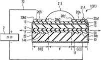
도 1a에 도시하는 바와 같이 이 제 1 실시예에 의한 파장 가변 반도체 레이저 소자(1A)(1)는, 광도파로가 활성 영역(A), 위상 조정 영역(B) 및 DBR 영역(C)의 3개의 영역으로 구성되는 DBR 레이저이다.As shown in Fig. 1A, in the wavelength tunable
그리고, 도 1a에 도시하는 바와 같이 다층의 반도체층을 제작하기 위한 반도 체 기판으로서의 n-InP 기판(10)의 윗쪽 중앙부에는, 단면이 사다리꼴 형상인 메사(10a)가 길이 방향(광의 출사 방향)을 연장해서 형성되어 있다.And as shown in FIG. 1A, in the upper center part of the n-InP board |
이 메사(10a)의 윗쪽에는 광을 생성하는 활성층(12), p-InP 클래드 층(13)이 순차적으로 적층되어 있다.On top of this
또한, 메사(10a)의 양측에는, p-InP 매립층(15) 및 n-InP 매립층(16)이 형성되어 있으므로, 후술하는 한 쌍의 전극 사이에 공급되는 전류 경로의 협착화가 확보되어 있는 동시에, 스트라이프형 광도파로가 형성되어 있다.In addition, since the p-InP buried
그리고, 이렇게 제작된 반도체층의 표리면에는 한 쌍의 전극(17, 18)으로서, Au 등의 금속막으로 이루어지는 n측 전극(제 1 구동용 전극:17)과 p측 전극(제 2 구동용 전극:18)이 각각 형성되어 있다.The n-side electrode (first driving electrode 17) and the p-side electrode (second driving electrode) made of a metal film such as Au as a pair of
또한, 도시되지 않았지만, p-InP 클래드 층(13)과 p측 전극(18) 사이에는 전류 주입을 쉽게 하기 위한 콘택트층이 형성되어 있어도 된다.Although not shown, a contact layer for facilitating current injection may be formed between the p-
이 콘택트층으로서 이용되는 재질은 p-InGaAs나 p-InGaAsP가 바람직하다.As a material used as this contact layer, p-InGaAs or p-InGaAsP is preferable.
도 1a의 예에서는, n-InP 기판(10)의 이면에 n측 전극(17)이 형성되고, p-InP 클래드 층(13)의 표면의 일부(좌측 앞 부분)에 p측 전극(18)이 형성되어 있다.In the example of FIG. 1A, the n-
반도체 레이저 소자(1A)에는, 광을 생성하는 활성층(12)이 형성되어 있는 활성 영역(A)과, 이 활성 영역(A)과 연속하여 이루어지는 제 1 수동 영역(이하, 위상 조정 영역(B)이라고 한다)과, 이 위상 조정 영역(B)과 연속하여 이루어지며, 한쪽 단부측(우측 부분)에 회절 격자(14)가 형성되어 있는 제 2 수동 영역(이하, 브래그 반사기 영역(DBR 영역(C))이라고 한다)으로 이루어지는 광이 분포되는 광도파로가 형성되어 있다.In the
또한, 참조 부호(11)는 광도파로의 일부를 형성하는 광 가이드층이다.
또한, p-InP 클래드 층(13)의 표면의 위상 조정 영역(B) 상에는 예컨대, Pt나 Au 등의 박막 저항으로 이루어지는 가열부(20)가 절연막(19)을 거쳐서 형성되어 있다.In addition, on the phase adjusting region B on the surface of the p-
이 가열부(20)에는 제 1 가열용 단자(20a) 및 제 2 가열용 단자(20b)가 형성되어 있다.In this
그리고, 이 가열부(20)는 외부의 단일의 전원(2)에 대하여 한 쌍의 전극(17, 18)과 직렬로 배선 접속되어 있다.And this
이 경우, 제 2 구동용 전극(p측 전극:18)과 상기 제 1 가열용 단자(20a) 사이가, 본딩 와이어 등에 의한 제 1 접속 선로(21)로 접속되어 있는 동시에, 제 1 구동용 전극(n측 전극:17)과 제 2 가열용 단자(20b) 사이가 외부의 전원(2)을 거쳐서, 본딩 와이어 등에 의한 제 2 접속 선로(22)로 접속되어 있다.In this case, between the 2nd driving electrode (p-side electrode) 18 and the said
이에 따라, 도 2a에 도시하는 바와 같이 파장 가변 반도체 레이저 소자(1)에 있어서의 한 쌍의 전극(17, 18)과 가열부(20)가 외부의 단일의 전원(2)에 대하여 직렬 접속되어 있는 등가 회로가 구성된다.As a result, as shown in FIG. 2A, the pair of
그리고, 가열부(20) 및 한 쌍의 전극(17, 18) 사이 양쪽에는 외부의 단일 전원(2)으로부터의 한 채널의 전류가 구동 전원으로서 동시에 공급된다.Then, both channels between the
즉, 도 1a에 도시하는 바와 같이 이 제 1 실시예의 파장 가변 반도체 레이저 소자(1)에 있어서, 파장 제어 영역(D)은, 해당 파장 제어 영역(D)의 일부에 구비되 어 있는 회절 격자(14)로 이루어지는 분포 브래그 반사기(Distributed Bragg Reflector:DBR) 영역(C)과, 해당 DBR 영역(C)에 인접되어 있는 위상 조정 영역(B)으로 이루어진다.That is, as shown in FIG. 1A, in the tunable
그리고, 가열부(20)는, 파장 제어 영역(D)에 포함되어 있는 위상 조정 영역(B)을 가열할 때, 위상 조정 영역(B)의 적어도 일부를 가열할 수 있도록 구성되어 있다.And the
이에 따라, 제 1 실시예에 의하면, 가열부(20)에 의해서 위상 조정 영역(B)의 적어도 일부를 가열하여, 해당 부분의 광도파로의 굴절율을 크게 변화시켜, 활성층(12)에서 생성된 광의 파장과 레이저 출력을 소망하는 파장 가변폭으로 한 채널의 전류에 의해 제어 가능하게 하는 파장 가변 반도체 레이저 소자(1)를 실현할 수 있다.Accordingly, according to the first embodiment, at least a part of the phase adjusting region B is heated by the
또한, 제 1 실시예에 의하면, 외부의 단일의 전원(2)을 겸용하여 활성층(12)에서 생성되는 광의 파장과 레이저 출력을 제어할 수 있어, 구조도 간이하게 됨으로써, 개체 내에 전원을 하나 밖에 마련할 수 없는 휴대식 가스 검지 장치에 적용하는 경우에도, 그 실장에 있어서의 설치 공간을 가급적 작게 할 수 있는 파장 가변 반도체 레이저 소자(1)를 실현할 수 있다.In addition, according to the first embodiment, the external
또한, 제 1 실시예에 의하면, 가열부(20)가 위상 조정 영역(B) 상에만 형성되어, 광을 생성하는 활성 영역(A)을 가열부(20)로 직접 가열하지 않는 구성으로 이루어지므로, 장기 수명화를 가능하게 하는 파장 가변 반도체 레이저 소자(1)를 실현할 수 있다.In addition, according to the first embodiment, since the
또한, 상술한 제 1 실시예에서는, 가열부(20)를 위상 조정 영역(B) 상에만 형성한 예로 설명했지만, 이에 한정되는 것은 아니다.In addition, in the above-mentioned 1st Example, although the
예컨대, 도 1b에 도시하는 바와 같이 가열부(20)가 위상 조정 영역(B) 전체 또는 일부에 더해서 DBR 영역(C) 전역을 균일하게 가열하는 것과 같은 구성이여도 된다.For example, as shown in FIG. 1B, the structure in which the
(제 1 실시예의 변형예)(Modification of the first embodiment)
다음으로, 본 발명에 관한 파장 가변 반도체 레이저 소자의 제 1 실시예의 변형예에 대하여 도 1b를 참조하면서 설명한다.Next, a modification of the first embodiment of the tunable semiconductor laser device according to the present invention will be described with reference to FIG. 1B.
도 1b는 본 발명에 관한 파장 가변 반도체 레이저 소자의 제 1 실시예의 변형예의 구성을 나타내는 개략 사시도이다.1B is a schematic perspective view showing the configuration of a modification of the first embodiment of the tunable semiconductor laser device according to the present invention.
또한, 도 1b에서 상술한 도 1a에 도시한 제 1 실시예에 의한 파장 가변 반도체 레이저 소자와 동일하게 구성되는 부분에는, 도 1a에서와 동일한 참조 부호를 부여하며 설명은 생략하는 것으로 한다.1B, the same reference numerals as those in FIG. 1A will be given to the same parts as those in the tunable semiconductor laser device according to the first embodiment shown in FIG. 1A.
즉, 도 1b에 도시하는 바와 같이 이 제 1 실시예의 변형예에 의한 파장 가변 반도체 레이저 소자(1)에 있어서, 파장 제어 영역(D)은 상술한 제 1 실시예의 경우와 같이, 해당 파장 제어 영역(D)의 일부에 구비되어 있는 회절 격자(14)로 이루어지는 분포 브래그 반사형(Distributed Bragg Reflector:DBR) 영역(C)과, 해당 DBR 영역(C)에 인접되어 있는 위상 조정 영역(B)으로 이루어진다.That is, as shown in Fig. 1B, in the tunable
그리고, 가열부(20)는 파장 제어 영역(D)에 포함되는 위상 조정 영역(B)과 DBR 영역(C)을 가열할 때, 위상 조정 영역(B)의 적어도 일부를 가열할 수 있도록 구성되어 있는 동시에, DBR 영역(C) 전역을 균일하게 가열할 수 있도록 구성되어 있다.The
이에 따라, 제 1 실시예의 변형예에 의하면, 가열부(20)에 의해서 위상 조정 영역(B)의 적어도 일부를 가열하는 동시에, DBR 영역(C) 전역을 균일하게 가열하여, 해당 부분의 광도파로의 굴절율을 상술한 제 1 실시예의 경우보다도 더 크게 변화시켜, 활성층(12)에서 생성된 광의 파장과 레이저 출력을 소망하는 파장 가변폭으로 한 채널의 전류에 의해 제어 가능하게 하는 파장 가변 반도체 레이저 소자(1)가 실현된다.Accordingly, according to the modification of the first embodiment, the
(제 2 실시예)(Second embodiment)
다음으로, 본 발명의 파장 가변 반도체 레이저 소자의 제 2 실시예에 대하여 도 3을 참조하면서 구체적으로 설명한다.Next, a second embodiment of the tunable semiconductor laser device of the present invention will be described in detail with reference to FIG.
도 3은 본 발명에 관한 파장 가변 반도체 레이저 소자의 제 2 실시예의 구성을 나타내는 개략 사시도이다.3 is a schematic perspective view showing the configuration of a second embodiment of a tunable semiconductor laser device according to the present invention.
도 3에 도시하는 바와 같이 이 제 2 실시예의 파장 가변 반도체 레이저 소자(1B(1))는, 활성층(12)의 하층에 있는 광 가이드층(11) 전역에 걸쳐서 회절 격자(14)가 형성되어 있는 DFB 레이저이다.As shown in FIG. 3, in the tunable
도 3에 도시하는 바와 같이 다층의 반도체층을 제작하기 위한 반도체 기판으로서의 n-InP 기판(10)의 윗쪽 중앙부에는, 단면이 사다리꼴 형상인 메사(10a)가 길이 방향(광의 출사 방향)으로 연장해서 형성되어 있다.As shown in FIG. 3, in the upper center part of the n-
그리고, 이 메사(10a) 중에는, 전역에 걸쳐서 회절 격자(14)가 형성되어 있는 광 가이드층(11)과, 광을 생성하는 활성층(12)과, p-InP 클래드 층(13)이 순차적으로 적층되어 있다.In this
또한, 메사(10a) 양측에는, p-InP 매립층(15) 및 n-InP 매립층(16)이 형성되어 있음으로써, 후술하는 한 쌍의 전극 사이에 공급되는 전류 경로의 협착화가 확보되는 동시에, 스트라이프형 광도파로가 형성된다.In addition, since the p-InP buried
그리고, 이렇게 제작된 반도체층의 표리면에는, 한 쌍의 전극(17, 18)으로서, Au 등의 금속막으로 이루어지는 n측 전극(제 1 구동용 전극:17)과 p측 전극(제 2 구동용 전극:18)이 각각 형성되어 있다.The n-side electrode (first driving electrode: 17) and the p-side electrode (second driving) made of a metal film such as Au as a pair of
도 3의 예에서는, n-InP 기판(10)의 이면에 n측 전극(17)이 형성되고, p-InP 클래드 층(13)의 표면의 일부분(활성층(12) 위를 제외한 우측의 거의 절반부)에 p측 전극(18)이 형성되어 있다.In the example of FIG. 3, an n-
또한, p-InP 클래드 층(13)의 상면에는, 예컨대, Pt나 Au 등의 박막 저항으로 이루어지는 가열부(20)가 파장 제어 영역(D)으로서 광 가이드층(11) 전역에 걸쳐서 형성되어 있는 회절 격자(14) 전역을 덮도록 절연막(19)을 사이에 두고 형성되어 있다.In addition, on the upper surface of the p-
이 가열부(20)에는 제 1 가열용 단자(20a) 및 제 2 가열용 단자(20b)가 형성되어 있다.In this
그리고, 이 가열부(20)는 외부의 단일 전원(2)에 대하여, 한 쌍의 전극(17, 18)과 직렬로 배선 접속되어 있다.And this
이 경우, 제 2 구동용 전극(p측 전극:18)과 상기 제 1 가열용 단자(20a) 사이가 본딩 와이어 등에 의한 제 1 접속 선로(21)로 접속되어 있는 동시에, 제 1 구동용 전극(n측 전극:17)과 제 2 가열용 단자(20b) 사이가 외부 전원(2)을 거쳐서, 본딩 와이어 등에 의한 제 2 접속 선로(22)로 접속되어 있다.In this case, the second driving electrode (p-side electrode) 18 and the
이에 따라, 도 2a에 도시하는 바와 같이 파장 가변 반도체 레이저 소자(1)에 있어서의 한 쌍의 전극(17, 18)과 가열부(20)가 외부의 단일의 전원(2)에 대하여 직렬 접속되어 있는 등가 회로가 구성된다.As a result, as shown in FIG. 2A, the pair of
그리고, 가열부(20)와 한 쌍의 전극(17, 18) 사이 양쪽에는, 외부의 단일 전원(2)으로부터 한 채널의 전류가 구동 전원으로서 동시에 공급된다.Then, both channels between the
이에 따라, 제 2 실시예에 의하면 광 가이드층(11) 전역에 걸쳐서 형성되어 있는 회절 격자(14) 전역을 가열부(20)에 의해서 가열하여, 해당 부분의 광도파로의 굴절율을 크게 변화시킴으로써, 활성층(12)에서 생성된 광의 파장과 레이저 출력을 소망하는 파장 가변폭으로 한 채널의 전류에 의해 제어 가능하게 하는 파장 가변 반도체 레이저 소자(1)를 실현할 수 있다.Accordingly, according to the second embodiment, the
또한, 제 2 실시예에 의하면, 외부의 단일 전원(2)을 겸용하여 활성 영역(A)에서 생성된 광의 파장과 레이저 출력을 제어할 수 있고, 구조도 간이하게 되어, 케이싱 내에 전원을 하나밖에 마련할 수 없는 휴대식 가스 검지 장치에 적용하는 경우에도, 그 실장시의 설치 공간을 가급적 작게 할 수 있는 파장 가변 반도체 레이저 소자(1)를 실현할 수 있다.In addition, according to the second embodiment, the external
(제 3 실시예)(Third embodiment)
다음으로, 본 발명의 파장 가변 반도체 레이저 소자의 제 3 실시예에 대하여 도 4를 참조하면서 구체적으로 설명한다.Next, a third embodiment of the tunable semiconductor laser device of the present invention will be described in detail with reference to FIG.
도 4는 본 발명에 관한 파장 가변 반도체 레이저 소자의 제 3 실시예의 구성을 나타내는 단면도이다.4 is a cross-sectional view showing the configuration of the third embodiment of the tunable semiconductor laser device according to the present invention.
도 4에 도시하는 바와 같이 이 제 3 실시예의 파장 가변 반도체 레이저 소자(1C(1))는, 제 2 실시예의 반도체 레이저 소자(1B(1))에서 형성되어 있는 회절 격자(14)가 활성층(12) 위의 전역이 아니라, 출사 방향 단면측에 부분적으로 형성되어 있는 부분 회절 격자형 반도체 레이저(PC-LD)이다.As shown in Fig. 4, in the tunable
그리고, 회절 격자(14)의 윗쪽에는 광 가이드층(11)과, 광을 생성하는 활성층(12)과, p-InP 클래드 층(13)이 순차적으로 적층되어 있다.On the upper side of the
그 다음, 제 2 실시예와 같이 p-InP 매립층 및 n-InP 매립층(도시 생략)이 통상의 매립 성장에 의해 형성된다.Then, as in the second embodiment, a p-InP buried layer and an n-InP buried layer (not shown) are formed by normal buried growth.
그리고, 레이저 출사면에 반사 방지막(AR 코트:23)가 형성됨과 동시에, 반대면에 고반사막(HR 코트:24)이 형성된다.An antireflection film (AR coat) 23 is formed on the laser exit surface, and a high reflection film (HR coat 24) is formed on the opposite surface.
그리고, 제작된 반도체 결정의 표리면에는, 한 쌍의 전극(17, 18)으로서 금속 전극으로 이루어지는 n측 전극(제 1 구동용 전극:17)과 p측 전극(제 2 구동용 전극:18)이 각각 형성되어 있다.The n-side electrode (first driving electrode 17) and the p-side electrode (second driving electrode 18) made of a metal electrode as a pair of
도 4의 예에서는, n-InP 기판(10)의 이면에 n측 전극(17)이 형성되고, p-InP 클래드 층(13)의 표면의 일부(좌측 부분)에 p측 전극(18)이 형성되어 있다.In the example of FIG. 4, the n-
또한, p-InP 클래드 층(13) 상면에는, 예컨대, Pt나 Au 등의 박막 저항으로 이루어지는 가열부(20)가 절연막(19)을 거쳐서, 출사면측에 부분적으로 형성되어 있는 회절 격자(14) 전역을 피복하도록 형성되어 있다.In addition, a
이 가열부(20)에는 제 1 가열용 단자(20a) 및 제 2 가열용 단자(20b)가 형성되어 있다.In this
그리고, 이 가열부(20)는 외부의 단일의 전원(2)에 대하여, 한 쌍의 전극(17, 18)과 직렬로 배선 접속되어 있다.And this
이 경우, 제 2 구동용 전극(p측 전극:18)과 상기 제 1 가열용 단자(20a) 사이가 본딩 와이어 등에 의한 제 1 접속 선로(21)로 접속되어 있는 동시에, 제 1 구동용 전극(n측 전극:17)과 제 2 가열용 단자(20b) 사이가 외부의 전원(2)을 거쳐서, 본딩 와이어 등에 의한 제 2 접속 선로(22)로 접속되어 있다.In this case, the second driving electrode (p-side electrode) 18 and the
이에 따라, 도 2a에 도시하는 바와 같이 파장 가변 반도체 레이저 소자(1)에 있어서의 한 쌍의 전극(17, 18)과 가열부(20)가 외부의 단일 전원(2)에 대하여 직렬 접속되어 있는 등가 회로가 구성된다.Thereby, as shown in FIG. 2A, the pair of
그리고, 가열부(20)과 한 쌍의 전극(17, 18) 사이의 양쪽에는, 외부의 단일 전원(2)으로부터 한 채널의 전류가 구동 전원으로서 동시에 공급된다.Then, both channels between the
이에 따라, 제 3 실시예에 의하면, 가이드층(11)의 출사면측에 부분적으로 형성되어 있는 회절 격자(14) 전역을 가열부(20)에 의해서 가열하여, 해당 부분의 가이드층 n의 굴절율을 크게 변화시킴으로써, 활성층(12)에서 생성된 광의 파장과 레이저 출력을 소망하는 파장 가변폭으로 한 채널의 전류에 의해 제어 가능하게 하 는 파장 가변 반도체 레이저 소자(1)를 실현할 수 있다.Accordingly, according to the third embodiment, the
또한, 제 3 실시예에 의하면, 외부의 단일의 전원(2)을 겸용하여 활성층(12)에서 생성된 광의 파장과 레이저 출력을 제어할 수 있고, 구조도 간이하게 됨으로써, 개체 내에 전원을 하나밖에 마련할 수 없는 휴대식 가스 검지 장치에 적용하는 경우에도, 그 실장시의 설치 공간을 가급적 작게 할 수 있는 파장 가변 반도체 레이저 소자(1)를 실현할 수 있다.In addition, according to the third embodiment, the wavelength of the light generated in the
(제 4 실시예)(Example 4)
다음으로, 본 발명의 파장 가변 반도체 레이저 소자의 제 4 실시예에 대하여 도 5를 참조하면서 구체적으로 설명한다.Next, a fourth embodiment of the tunable semiconductor laser device of the present invention will be described in detail with reference to FIG.
도 5는 본 발명에 관한 파장 가변 반도체 레이저 소자의 제 4 실시예의 구성을 나타내는 단면도이다.5 is a cross-sectional view showing the configuration of the fourth embodiment of the tunable semiconductor laser device according to the present invention.
도 5에 도시하는 바와 같이 이 제 4 실시예의 파장 가변 반도체 레이저 소자(1D(1))는, 다층의 반도체 층을 제작하기 위한 반도체 기판으로서의 n-InP 기판(10)의 윗쪽에, n-InGaAsP로 이루어지는 제 1 회절 격자 영역(E)과, 위상 시프트 영역(F)과, n-InGaAsP로 이루어지는 제 2 회절 격자 영역(G)이 형성되어 있다.As shown in Fig. 5, the tunable
이 경우, 제 1 및 제 2 회절 격자 영역(E, G)에는 각각, 제 1 및 제 2 회절 격자(14a, 14b)가 형성되어 있다.In this case, first and
또한, 가이드층(11)의 윗쪽에는 각각, 적당한 조성의 InGaAsP로 이루어진 하측 SCH층, MQW층, 상측 SCH 층을 포함하는 광을 생성하는 활성층(12)이 형성되어 있다.Further, on the upper side of the
이 활성층(12)의 윗쪽에는 p-InP 클래드 층(13)이 형성되어 있다.The p-InP clad
그리고, 제작된 반도체 층의 표리면에는, 한 쌍의 전극(17, 18)으로서, 금속 전극으로 이루어지는 n측 전극(제 1 구동용 전극:17)과 p측 전극(제 2 구동용 전극:18)이 형성되어 있다.The n-side electrode (first driving electrode 17) and the p-side electrode (second driving electrode: 18) made of metal electrodes are formed on the front and back surfaces of the produced semiconductor layer as a pair of
도 5의 예에서는, p-InP 클래드 층(13)의 윗쪽의 소정 위치에 p측 전극(18)이 형성되고, n-InP 기판(10)의 하면에 n측 전극(17)이 형성되어 있다.In the example of FIG. 5, the p-
또한, 레이저 광이 출사되는 광도파로로서의 가이드층(11)의 각 단면(적어도 한쪽이여도 된다)에는, 반사 방지막(23)이 형성되어 있다.Moreover, the
또한, p-InP 클래드 층의 윗쪽에서, 제 1 및 제 2 회절 격자 영역(E, G)과 대향하는 부위에 각각, 예컨대, Pt나 Au 등의 박막 저항으로 이루어지는 제 1 및 제 2 가열부(20A, 20B)가 절연층(19)을 사이에 두고 제 1 및 제 2 회절 격자(14a), 14b) 각각의 전역을 피복하도록 형성되어 있다.Further, on the upper side of the p-InP clad layer, first and second heating parts each made of thin film resistors such as Pt and Au, respectively, at the portions facing the first and second diffraction grating regions E and G ( 20A and 20B are formed so as to cover the entire area of each of the first and
이들 제 1 및 제 2 가열부(20A, 20B)에는 각각, 제 1 가열용 단자(20a1, 20a2) 및 제 2 가열용 단자(20b1, 20b2)가 형성되어 있다.In these 1st and
이들 제 1 및 제 2 가열부(20A, 20B)는 외부의 단일 전원(2)에 대하여, 한 쌍의 전극(17, 18)과 직렬로 배선 접속되어 있다.These 1st and
이 경우, 제 2 구동용 전극(p측 전극:18)과 제 1 가열부(20A)의 제 1 가열용 단자(20a1) 사이가 본딩 와이어 등에 의한 제 1 접속 선로(21A)에 접속되는 동시에, 제 1 가열부(20A)의 제 2 가열용 단자(20b1)와 제 2 가열부(20B)의 제 1 가열 용 단자(20a2) 사이가, 본딩 와이어 등에 의한 중계용 접속 선로(21B)에 접속되어 있다.In this case, between the second driving electrode (p-side electrode) 18 and the first heating terminal 20a1 of the
또한, 제 1 구동용 전극(n측 전극:17)과 제 2 가열부(20B)의 제 2 가열용 단자(20b2) 사이가 외부 전원(2)을 거쳐서 본딩 와이어 등에 의한 제 2 접속 선로(22)에 접속되어 있다.In addition, a
이에 따라, 도 2b에 도시하는 바와 같이 파장 가변 반도체 레이저 소자(1)에 있어서의 한 쌍의 전극(17, 18)과 제 1 및 제 2 가열부(20A, 20B)가 외부의 단일 전원(2)에 대하여 직렬 접속된 등가 회로가 구성된다.As a result, as shown in FIG. 2B, the pair of
그리고, 제 1 및 제 2 가열부(20A, 20B) 및 한 쌍의 전극(17, 18) 사이의 양쪽에는, 외부의 단일의 전원(2)으로부터 한 채널의 전류가 구동 전원으로서 동시에 공급된다.Then, both of the first and
즉, 도 5에 도시하는 바와 같이 이 제 4 실시예의 파장 가변 반도체 레이저 소자(1)에 있어서, 파장 제어 영역(D)은 가이드층(11)에 형성되어 있는 제 1 및 제 2 회절 격자 영역(E, G)으로 이루어진다.That is, as shown in Fig. 5, in the tunable
그리고, 제 1 및 제 2 가열부(20A, 20B)가 각각, 파장 제어 영역(D)에 포함되는 제 1 및 제 2 회절 격자 영역(E, G)에 형성되어 있는 제 1 및 제 2 회절 격자(14a, 14b)를 가열할 때, 각 회절 격자에서 선택된 각 파장이 서로 같도록, 제 1 및 제 2 회절 격자(14a, 14b)를 가열할 수 있게 구성되어 있다.The first and second diffraction gratings, in which the first and
이러한 제 4 실시예에 의하면, 제 1 및 제 2 가열부(20A, 20B)에 의해서, 각각, 파장 제어 영역(D)에 포함되는 제 1 및 제 2 회절 격자 영역(E, G)에 형성되어 있는 제 1 및 제 2 회절 격자(14a, 14b)를 가열하여, 해당 부분의 광도파로의 굴절율을 크게 변화시켜, 활성층(12)에서 생성된 광의 파장과 레이저 출력을 소망하는 파장 가변폭으로 한 채널의 전류에 의해 제어 가능하게 하는 파장 가변 반도체 레이저 소자(1)를 실현할 수 있다.According to this fourth embodiment, the first and
또한, 제 4 실시예에 의하면, 외부의 단일 전원(2)을 겸용하여 활성층(12)에서 생성된 광의 파장과 레이저 출력을 제어할 수 있고, 구조도 간이하게 됨으로써, 개체 내에 전원을 하나밖에 마련할 수 없는 휴대식 가스 검지 장치에 적용하는 경우에도, 그 실장에 있어서의 설치 공간을 가급적 작게 할 수 있는 파장 가변 반도체 레이저 소자(1)를 실현할 수 있다.Further, according to the fourth embodiment, the wavelength of the light generated in the
(파장 특성에 대한 설명)(Description of wavelength characteristics)
다음으로, 본 발명에 의한 파장 가변 반도체 레이저 소자(1)와 종래의 파장 가변 반도체 레이저 소자의 파장 특성에 대하여 도 6 및 도 7을 참조하면서 구체적으로 설명한다.Next, the wavelength characteristics of the tunable
도 6은 종래의 파장 가변 반도체 레이저 소자의 출력 특성 및 파장 특성을 도시하는 도면이다.6 is a diagram showing output characteristics and wavelength characteristics of a conventional tunable semiconductor laser device.
도 7은 본 발명에 관한 파장 가변 반도체 레이저 소자의 출력 특성 및 파장 특성을 도시하는 도면이다.It is a figure which shows the output characteristic and wavelength characteristic of the tunable semiconductor laser element which concerns on this invention.
또한, 6 및 도 7에 있어서 실선으로 나타내는 특성은 각각 파장 가변 반도체 레이저 소자의 구동 전류[mA]에 대한 출력 특성(Power[mW])이고, 파선으로 나타내 는 특성은 각각 파장 가변 반도체 레이저 소자의 구동 전류[mA]에 대한 파장 특성(파장 시프트량 Δλ[nm])이다.In addition, in FIG. 6 and FIG. 7, the characteristic shown by the solid line is the output characteristic (Power [mW]) with respect to the drive current [mA] of a tunable semiconductor laser element, respectively, and the characteristic represented by a broken line is the characteristic of a tunable semiconductor laser element, respectively. It is wavelength characteristic (wavelength shift amount (DELTA) (lambda) [nm]) with respect to drive current [mA].
여기서는, 본 발명의 파장 가변 반도체 레이저 소자(1)로서 본 발명의 제 2 실시예에 의한 파장 가변 반도체 레이저 소자(1B)의 파장 특성과, 종래의 파장 가변 반도체 레이저 소자로서 예컨대, 도 9에 나타낸 가열부가 없는 DFB 레이저의 파장 특성을 예로 들어 설명한다.Here, the wavelength characteristics of the tunable
통상, 단일 모드 발진하는 파장 가변 반도체 레이저 소자로서는, 한 쌍의 전극 사이에 공급되는 구동 전류가 임계값 전류를 넘을 때에 광을 출사하고, 그 전류치의 2승에 비례하여 출사광의 파장이 커지는 특성을 갖는다.In general, as a tunable semiconductor laser device having a single mode oscillation, light is emitted when a drive current supplied between a pair of electrodes exceeds a threshold current, and the wavelength of the emitted light increases in proportion to the square of the current value. Have
그리고, 도 6에 도시하는 바와 같이 종래의 가열부가 없는 DFB 레이저의 파장 특성의 경우, 전류치를 증가시켜서 출력을 올려 가면, 도 6에서 파선으로 나타내는 파장 시프트량 Δλ이 완만한 기울기로 변화하고 있는 것을 알 수 있다.As shown in FIG. 6, in the case of the wavelength characteristic of the conventional DFB laser without a heating part, when the output value is increased by increasing the current value, the wavelength shift amount Δλ indicated by the broken line in FIG. 6 is changed to a gentle slope. Able to know.
이에 대하여, 도 7에 도시하는 바와 같이 본 발명의 제 2 실시예의 파장 가변 반도체 레이저 소자(1B)의 파장 특성의 경우, 파장 제어 영역(D)으로서 광 가이드층(11) 전역에 걸쳐서 형성되어 있는 회절 격자(14) 전역이 가열부(20)에 의해서 가열되기 때문에, 전류치를 늘려서 출력을 올려 가면, 종래의 가열부가 없는 DFB 레이저와 비교하여, 도 7에 파선으로 나타내는 파장 시프트량 Δλ의 기울기가 급하게 되어, Aλ의 변화량이 커졌다는 것을 알 수 있다.On the other hand, as shown in FIG. 7, in the case of the wavelength characteristic of the tunable
즉, 이는 종래의 가열부가 없는 파장 가변 반도체 레이저 소자의 굴절율 변화에 비교해서, 본 발명의 제 2 실시예의 파장 가변 반도체 레이저 소자가 광도파 로의 굴절율 변화가 보다 커졌다는 것을 나타내고 있다.That is, this indicates that the change in the refractive index of the optical waveguide is larger in the wavelength variable semiconductor laser device of the second embodiment of the present invention than in the refractive index change of the conventional tunable semiconductor laser device without a heating portion.
또한, 도 6 및 도 7의 예에서는 종래의 가열부가 없는 DFB 레이저와 본 발명의 제 2 실시예의 파장 가변 반도체 레이저 소자에서 나오는 파장 특성을 비교하고 있다.In addition, in the example of FIG. 6 and FIG. 7, the wavelength characteristic emitted from the conventional DFB laser without a heating part and the tunable semiconductor laser element of 2nd Example of this invention is compared.
그런데, 종래의 가열부가 없는 DFB 레이저의 파장 특성과, 본 발명의 제 1, 제 3, 제 4 실시예에 의한 파장 가변 반도체 레이저 소자(1A, 1C, 1D)에서 나오는 파장 특성의 비교에 있어서도, 상술한 바와 마찬가지의 비교 결과를 얻을 수 있다.By the way, also in the comparison of the wavelength characteristic of the conventional DFB laser without a heating part and the wavelength characteristic coming out from the tunable
또한, 본 발명의 제 1 실시예에 의한 파장 가변 반도체 레이저 소자(1A)와 제 2 내지 제 4 실시예에 의한 파장 가변 반도체 레이저 소자(1B, 1C, 1D)의 레이저 출력값을 비교한 경우, 가열부(20) 또는 제 1 및 제 2 가열부(20A, 20B)에 의해 활성층(12)을 직접 가열하는 파장 가변 반도체 레이저 소자(1B, 1C, 1D)의 경우에는, 레이저 출력값이 서서히 포화해 가는 데 대하여, 파장 가변 반도체 레이저 소자(1A)의 경우에는, 가열부(20)에 의해 활성 영역(A:활성층(12))이 직접 가열되지 않기 때문에, 레이저 출력값이 포화되기 어렵다는 결과를 얻을 수 있다(도시 생략).In addition, when the laser output values of the tunable
이는 제 1 실시예의 파장 가변 반도체 레이저 소자(1A)에 의한 DBR 레이저 쪽이, 제 2 내지 제 4 실시예에 의한 파장 가변 반도체 레이저 소자(1B, 1C, 1D)에 비교하여, 온도에 의한 굴절율 변화를 보다 크게 얻을 수 있다는 것을 나타내고 있다.This is because the DBR laser by the tunable
또한, 상술한 제 1 실시예의 파장 가변 반도체 레이저 소자(1A)는 가열 부(20)를 이용하여 활성 영역(A:활성층(12)) 이외의 영역을 가열하기 때문에, 활성 영역(A:활성층(12))이 가열되는 것에 의한 레이저 광의 출력 저감을 회피할 수 있기 때문에, 파장 가변 반도체 레이저 소자 자체의 수명을 늘릴 수 있다고 하는 효과를 갖고 있다.In addition, since the tunable
(제 5 실시예)(Example 5)
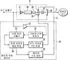
다음으로, 본 발명의 제 5 실시예로서, 상술한 본 발명의 제 1 내지 제 4 실시예에 의한 파장 가변 반도체 레이저 소자(1)를 적용한 가스 검지 장치의 개략 구성에 대하여 도 8a를 참조하면서 설명한다.Next, as a fifth embodiment of the present invention, a schematic configuration of a gas detection device to which the tunable
도 8a는 본 발명의 제 5 실시예로서 본 발명에 관한 파장 가변 도체 레이저 소자를 적용한 가스 검지 장치의 일례를 나타내는 개략 구성도이다.8A is a schematic block diagram showing an example of a gas detection apparatus to which the wavelength tunable laser device according to the present invention is applied as a fifth embodiment of the present invention.
도 8a에 도시하는 바와 같이 가스를 검지하는 가스 검지 장치(30)에 있어서는, 반도체 레이저 모듈(31)을 구성하는 원통형 케이스(32) 내측에 기판(33)이 설치된다.In the
그리고, 이 기판(33) 상에 설치되는 베이스대(34)의 표면에는, 펠티에 소자로 이루어지는 온도 제어 소자(35)가 부착되어 있다.And the
또한, 온도 제어 소자(35) 상에 설치된 부착대(36) 상에는, 상술한 본 발명의 제 1 내지 제 4 실시예 중 어느 한 실시예의 파장 가변 반도체 레이저 소자(1)가 탑재되어 있다.Further, on the mounting table 36 provided on the
이 경우, 파장 가변 반도체 레이저 소자(1)는, 원통형 케이스(32)의 중심축 상에 따라 레이저 광을 외부로 사출하는 것이 가능해지도록 배치되어 있다.In this case, the tunable
그리고, 파장 가변 반도체 레이저 소자(1)는, 검지 대상 가스의 농도를 측정하기 위한 레이저 광을 검지 대상으로 향해서 출사할 때에, 상세한 것은 후술하는 도 8b의 레이저 구동 제어부(50)의 온도 안정화 PID 회로(55)를 거쳐서 펠티에 소자로 이루어지는 온도 제어 소자(35)로 온도 제어됨으로써, 검지 대상 가스에 맞는 레이저 파장으로 제어된다.When the tunable
또한, 도 8a에 도시한 구성의 가스 검지 장치(30)의 경우, 파장 가변 반도체 레이저 소자(1)로부터의 레이저 광은 피 검지 가스측과 참조 가스측 쌍방으로 사출되도록 되어 있다.In addition, in the
또한 부착대(36) 상에서 파장 가변 반도체 레이저 소자(1) 양측에는, 피 검지 가스측 및 참조 가스측으로 출사되는 각 레이저 광을 집광하여 평행 빔으로 하기 위한 집광 렌즈(37, 38)가 레이저 광축 상에 위치하여 설치된다.On both sides of the variable-length
이에 따라, 파장 가변 반도체 레이저 소자(1)로부터 피 검지 가스측으로의 광은, 집광 렌즈(37) 및 반도체 레이저 모듈(31)을 보호하는 보호 유리(39)를 거쳐서 외부로 출력됨으로써 검지 공간 내로 출사된다.Accordingly, the light from the tunable
또한, 파장 가변 반도체 레이저 소자(1)로부터 참조 가스측으로의 광은 집광 렌즈(38)에서 평행 빔이 되며, 또한 참조 가스 셀(40)을 거쳐서 수광기(41)에서 수광되게 되어 있다.Further, the light from the tunable
여기서, 참조 가스 셀(40)은 참조 가스로서 검지 대상 가스를 봉입한 셀이며, 해당 참조 가스 셀(40)을 거쳐서 수광기(41)에 의해 수광된 참조 가스측으로의 광 빔의 수광 출력에 근거하여, 상세한 것은 후술하는 도 8b의 레이저 구동 제어부(50)의 파장 안정 제어 회로(54)에 의해, 파장 가변 반도체 레이저 소자(1)로부터 출사되는 레이저 광의 파장을 검지 대상 가스의 흡수 선파장에 맞추기 위한 것이다.Here, the
또한, 수광기(41)는 검지 공간으로 출사된 레이저 광이 반사하여 돌아오는 레이저 광을 수광하고, 이 수광한 레이저 광을 전기 신호(전류)로 변환하여 해당 전기 신호(전류)를. 상세한 것은 후술하는 도 8c의 가스 검출부(60)에 공급한다.The
그리고, 가스 검출부(60)는, 후술하는 바와 같이, 수광기(41)에 의해 변환된 전기 신호로부터 기본파 레벨 및 2배파 레벨을 검출하여, 2배파 레벨이 기본파 레벨로 나누어지고, 그 값에 근거하여 검지 대상 가스의 유무나 농도를 측정한다.As described later, the
또한, 도 8a 내지 도 8c 및 그 설명에 있어서, 이 제 5 실시예에 적용되는 본 발명의 제 1 내지 제 4 실시예에 의한 파장 가변 반도체 레이저 소자(1)가, 상술한 바와 같이, 한 쌍의 전극(17, 18)과 가열부(20)(20A, 20B)에 대해 외부의 단일 전원(2)에 직렬 접속되며, 한 쌍의 전극(17, 18)과 가열부(20)(20A, 20B)에 대하여 외부의 단일 전원(2)으로부터 동시에 구동 전류가 공급되는 구성에 대해서는 그 도시 및 그 작용 설명을 생략했다.8A to 8C and the description thereof, a pair of the tunable
도 8b는 반도체 레이저 모듈(31) 및 레이저 구동 제어부(50)의 개략 구성을 도시하는 도면이다.8B is a diagram illustrating a schematic configuration of the
레이저 구동 제어부(50)는 전류 전압 변환기(51)와, 기본파 신호 증폭기(52)와, 신호 미분 검출기(53)와, 파장 안정화 제어 회로(54)와, 온도 안정화 PID 회 로(55)와, 레이저 구동 회로(56)로 구성되어 있다.The
전류 전압 변환기(51)는 수광기(41)로부터의 전기 신호를 전압으로 변환한다. 기본파 신호 증폭기(52)는, 전류 전압 변환기(51)로 변환된 전압을 증폭한다. 신호 미분 검출기(53)는, 기본파 신호 증폭기(52)로 증폭된 전압 파형을 미분하여 참조 가스의 흡수 중심 파장 λ0으로부터의 편차 신호를 생성한다.The
파장 안정화 제어 회로(54)는 파장 가변형 반도체 레이저(1)의 발광 파장 λ을 참조 가스의 흡수 중심 파장 λ0으로 안정화시키는 제어를 행한다.The wavelength
즉, 파장 안정화 제어 회로(54)는 신호 미분 검출기(53)로부터의 편차 신호를 파장 가변형 반도체 레이저(1)의 온도로 변환하여 온도 안정화 PID 회로(55)에 출력하는 동시에, 그 편차 신호에 근거하여 제어 신호를 레이저 구동 회로(40)에 대하여 출력한다.That is, the wavelength
온도 안정화 PID 회로(55)는 펠티에 소자로 이루어진 온도 제어 소자(35)를 제어한다. 즉, 온도 안정화 PID 회로(55)는 파장 안정화 제어 회로(54)로부터의 온도 신호에 따라서 파장 가변형 반도체 레이저(1)가 소망하는 파장으로 발진하는 온도로 되도록 PID 제어를 하여, 파장 가변형 반도체 레이저(1)의 온도를 소정 온도로 안정되게 유지한다.The temperature
레이저 구동 회로(56)는 파장 가변형 반도체 레이저(1)의 발진 파장이 참조 가스(피측정 가스)의 흡수 특성의 흡수 중심 파장에 대응하는 값인 중심 전류치(바이어스 전류치)를 중심으로 하여, 소정의 진폭, 변조 주파수를 갖는 변조 신호(b) 를 반도체 레이저 모듈(31)에 조립된 파장 가변형 반도체 레이저(1)에 인가한다.The
그 결과, 반도체 레이저 모듈(31)로부터, 그 파장이 흡수 중심 파장을 중심으로 소정의 진폭, 주파수로 변화되는 레이저 광(a)이 출력된다.As a result, the laser light a whose wavelength is changed to a predetermined amplitude and frequency centering on the absorption center wavelength is output from the
또한, 레이저 구동 회로(56)는 파장 안정화 제어 회로(54)로부터의 온도 신호에 따라서 중심 전류치(바이어스 전류치)를 반도체 레이저 모듈(31)로부터 출력되는 레이저 광(a)에서의 상술한 파장 특성을 얻을 수 있도록 제어한다.In addition, the
이와 같이, 제 5 실시예에 관한 가스 검지 장치에서는 피측정 가스와 동일한 가스를 봉입한 참조 가스 셀(40)에 파장 가변형 반도체 레이저(1)로부터 출사되는 레이저 광을 투과시켜, 이 레이저 광의 중심 파장이 참조 가스(피측정 가스)의 흡수 특성의 흡수 중심 파장에 일치하도록, 파장 가변형 반도체 레이저(1)의 온도와 파장 가변형 반도체 레이저(1)에 전압을 가하는 변조 신호(b)의 중심 전류치(바이어스 전류치)가 자동적으로 제어된다.Thus, in the gas detection apparatus which concerns on 5th Example, the laser beam radiate | emitted from the
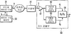
도 8c는, 도 8a의 가스 검지 장치 및 가스 검출부(60)의 개략 구성을 도시하는 도면이다. 도 8c에서 반도체 레이저 모듈(31)로부터 출력된 흡수 중심 파장을 중심으로 파장 변조된 레이저 광(a)은 피측정 가스를 투과하는 과정에서 흡수 특성에 따라 흡수된 후, 수광기(41)에서 수광되어 전기(전류) 신호(c)로 변환되어 가스 검출부(60)로 입력된다.FIG. 8C is a diagram illustrating a schematic configuration of the gas detection device and the
또한, 도 8c에서는, 설명의 상황상, 수광기(41)를 반도체 레이저 모듈(31)로부터 독립해서 도시하고 있다.In addition, in FIG. 8C, the
또한, 도 8c의 레이저 구동 제어부(50)의 상세한 구성 및 그 작용에 대해서 는 도 8b를 참조하여 앞에 설명되어 있다.In addition, the detailed structure and operation | movement of the laser
가스 검출부(60)는 전류 전압 변환기(61)와, 기본파 신호 검출기(62)와, 2배파 신호 검출기(63)와, 나눗셈기(64)로 구성되어 있다.The
전류 전압 변환기(61)는 입력한 전류의 전기(전류) 신호(c)를 전압의 전기 신호(c)로 변환하여 기본파 신호 검출기(62) 및 2배파 신호 검출기(63)로 송출한다.The
기본파 신호 검출기(62)는 입력한 전기 신호(c)에 포함되어 있는 변조 주파수의 신호 성분인 기본파 신호(d1)를 추출하여 나눗셈기(64)로 송출한다.The fundamental
2배파 신호 검출기(63)는 입력한 전기 신호(c)에 포함되는 변조 주파수의 2배의 주파수의 신호 성분인 2배파 신호(d2)를 추출하여 나눗셈기(64)로 송출한다.The double-
나눗셈기(64)는 2배파 신호(d2)의 진폭(D2)과 기본파 신호(d1)의 진폭(D 1)의 비(D2/D1)를 산출하고, 이 산출한 비(D2/D1)를 이 가스 농도에 대응하는 검출값 D(=D2/D1)으로서 출력한다.Calculated the
이상 상술한 바와 같이, 본 발명에 의한 파장 가변 반도체 레이저 소자(1)는 한 쌍의 전극(17, 18)과 가열부(20)(20A, 20B)가 외부의 단일 전원(2)에 직렬 접속되고, 한 쌍의 전극(17, 18)과 가열부(20)(20A, 20B)에 대하여 외부의 단일 전원(2)으로부터 동시에 구동 전류가 공급되는 구성으로 되어 있다.As described above, in the tunable
이에 따라, 본 발명에 의한 파장 가변 반도체 레이저 소자(1)를 적용하여 TDLAS 법에 의한 가스 검지를 할 때, 굴절율 변화를 크게 하여 소망하는 파장 가변폭으로 파장을 레이저 출력과 동시에 한 채널의 전류로 제어할 수 있다.Accordingly, when the gas detection by the TDLAS method is applied by applying the tunable
또한, 레이저 출력과 파장을 제어할 때, 단일 전원을 겸용하기 때문에 전원도 하나만으로 해결할 수 있다.In addition, when controlling the laser output and wavelength, a single power supply can be used to solve even a single power supply.
그 결과, 본 발명에 의한 파장 가변 반도체 레이저 소자(1)의 구조도 간이하게 되고, 소비 전력도 작은 케이싱 내의 부품 설치 공간이나 전원 용량이 제한되는 휴대식 가스 검지 장치(30)에도 내장하여 사용할 수 있다.As a result, the structure of the tunable
또한, 제 1 실시예에 의한 파장 가변 반도체 레이저 소자를 채용하면, 가열부(20)가 활성 영역(A:활성층(12))을 직접 가열하지 않는 구성이기 때문에, 소자 자신의 장기 수명화를 도모할 수 있다.In addition, when the tunable semiconductor laser device according to the first embodiment is adopted, the
그런데, 상술한 제 3 또는 제 4 실시예에 의한 파장 가변 반도체 레이저 소자(1C, 1D)는, 반사 방지막(21)에 끼워진 영역 내의 한쪽 단부 또는 양단에 회절 격자(14)가 설치된다.By the way, in the variable-wavelength
그런데, 본 발명은 이러한 구성에 한정되는 것이 아니라, 광도파로 중 적어도 하나의 회절 격자 영역을 갖는 파장 가변 반도체 레이저 소자에도 본 발명의 구성(한 쌍의 전극과 가열부를 단일 전원에 대하여 직렬 접속하는 구성)을 채용할 수 있다.Incidentally, the present invention is not limited to such a configuration, but the configuration of the present invention also includes a wavelength tunable semiconductor laser device having at least one diffraction grating region of an optical waveguide (a configuration in which a pair of electrodes and a heating unit are connected in series with a single power source). ) Can be employed.
즉, 본 발명의 파장 가변 반도체 레이저 소자(1)는 바람직하게는 모드 호핑하지 않는 영역 상에 가열부(20)(20A, 20B)를 배치하고, 한 쌍의 전극(17, 18)과 가열부(20)(20A, 20B)를 외부의 단일 전원에 대하여 직렬 접속하는 구성으로 하면 된다.That is, the tunable
이상, 본 발명에 의한 최선의 실시예에 대하여 설명했지만, 이 최선의 실시예에 의한 기술 및 도면에 의해 본 발명이 한정되는 것은 아니다.As mentioned above, although the best embodiment by this invention was described, this invention is not limited by the technique and drawing by this best embodiment.
즉, 이 최선의 실시예에 근거하여 당업자 등에 의해 이루어지는 다른 실시예, 실시예 및 운용 기술 등은 전부 본 발명의 범주에 포함되는 것은 물론이다.That is, of course, all other embodiments, embodiments, operational techniques, etc. made by those skilled in the art based on this best embodiment are included in the scope of the present invention.
Claims (28)
Translated fromKoreanApplications Claiming Priority (2)
| Application Number | Priority Date | Filing Date | Title |
|---|---|---|---|
| JP2005077373AJP4231854B2 (en) | 2005-03-17 | 2005-03-17 | Semiconductor laser element and gas detector |
| JPJP-P-2005-00077373 | 2005-03-17 |
Publications (2)
| Publication Number | Publication Date |
|---|---|
| KR20070015201Atrue KR20070015201A (en) | 2007-02-01 |
| KR100799782B1 KR100799782B1 (en) | 2008-01-31 |
Family
ID=36991771
Family Applications (1)
| Application Number | Title | Priority Date | Filing Date |
|---|---|---|---|
| KR1020067024014AExpired - Fee RelatedKR100799782B1 (en) | 2005-03-17 | 2006-03-17 | Tunable semiconductor laser device, manufacturing method thereof, and gas detecting device using same |
Country Status (6)
| Country | Link |
|---|---|
| US (1) | US7620078B2 (en) |
| EP (1) | EP1737089B1 (en) |
| JP (1) | JP4231854B2 (en) |
| KR (1) | KR100799782B1 (en) |
| CN (1) | CN100481659C (en) |
| WO (1) | WO2006098427A1 (en) |
Cited By (1)
| Publication number | Priority date | Publication date | Assignee | Title |
|---|---|---|---|---|
| KR100959170B1 (en)* | 2008-02-26 | 2010-05-24 | 한국광기술원 | Fabrication method of self-oscillating multi-region DVF laser diode with integrated metal thin film heater |
Families Citing this family (35)
| Publication number | Priority date | Publication date | Assignee | Title |
|---|---|---|---|---|
| JP4231854B2 (en)* | 2005-03-17 | 2009-03-04 | アンリツ株式会社 | Semiconductor laser element and gas detector |
| US20100168405A1 (en) | 2006-08-11 | 2010-07-01 | Toyo Boseki Kabushiki Kaisha | Activator including biosurfactant as active ingredient, mannosyl erythritol lipid, and production method thereof |
| JP4850757B2 (en) | 2007-03-08 | 2012-01-11 | 日本電信電話株式会社 | Wavelength tunable semiconductor laser device, control device and control method thereof |
| DE102007039219B4 (en)* | 2007-08-20 | 2010-04-22 | Fraunhofer-Gesellschaft zur Förderung der angewandten Forschung e.V. | Spectrally tunable laser module |
| US8149890B2 (en)* | 2008-12-04 | 2012-04-03 | Electronics And Telecommunications Research Institute | Multiple distributed feedback laser devices |
| US7864824B2 (en) | 2008-12-04 | 2011-01-04 | Electronics And Telecommunications Research Institute | Multiple distributed feedback laser devices |
| EP3739635B1 (en)* | 2010-06-30 | 2022-03-09 | Alcatel Lucent | A device comprising an active component and associated electrodes and a method of manufacturing such device |
| JP5919682B2 (en)* | 2011-08-26 | 2016-05-18 | 富士通株式会社 | Semiconductor laser device |
| DE102012202893B3 (en)* | 2012-02-27 | 2013-01-17 | Siemens Aktiengesellschaft | Method for measuring concentration of gas component in measuring gas for visual gas analysis, involves triggering and producing current signals and burst-current signals such that signals are modified with directly generated current signals |
| JP6155770B2 (en)* | 2013-03-29 | 2017-07-05 | 富士通株式会社 | Optical element and optical module |
| USD734187S1 (en)* | 2013-06-24 | 2015-07-14 | New Cosmos Electric Co., Ltd. | Gas detector |
| JP6277660B2 (en)* | 2013-10-16 | 2018-02-14 | 住友電気工業株式会社 | Full duplex optical transceiver |
| WO2015081220A1 (en)* | 2013-11-30 | 2015-06-04 | Thorlabs Quantum Electronics, Inc. | Tunable semiconductor radiation source |
| US9537287B2 (en) | 2014-10-08 | 2017-01-03 | Futurewei Technologies, Inc. | Thermal compensation for burst-mode laser wavelength drift |
| US9246307B1 (en)* | 2014-10-08 | 2016-01-26 | Futurewei Technologies, Inc. | Thermal compensation for burst-mode laser wavelength drift |
| US20180083421A1 (en) | 2015-03-06 | 2018-03-22 | Apple Inc. | Independent control of emission wavelength and output power of a semiconductor laser |
| US11437779B2 (en)* | 2015-04-30 | 2022-09-06 | Apple Inc. | Vernier effect DBR lasers incorporating integrated tuning elements |
| DE102015119226A1 (en)* | 2015-11-09 | 2017-05-11 | Osram Opto Semiconductors Gmbh | Semiconductor laser diode |
| KR102729488B1 (en)* | 2016-11-08 | 2024-11-12 | 삼성전자주식회사 | Spectrometer, apparatus and method for measuring bio-information |
| CN107093839B (en)* | 2017-06-14 | 2024-04-09 | 西安炬光科技股份有限公司 | Semiconductor laser wavelength stabilizing system and implementation method |
| EP3688849A1 (en) | 2017-09-28 | 2020-08-05 | Apple Inc. | Laser architectures using quantum well intermixing techniques |
| US11552454B1 (en)* | 2017-09-28 | 2023-01-10 | Apple Inc. | Integrated laser source |
| CN108336634A (en)* | 2018-04-17 | 2018-07-27 | 大连藏龙光电子科技有限公司 | Tunable Laser Transmitter Heat Sink for Next Generation PON Technology |
| US11171464B1 (en) | 2018-12-14 | 2021-11-09 | Apple Inc. | Laser integration techniques |
| CN111089850B (en)* | 2020-02-17 | 2021-09-28 | 北京航空航天大学 | Multi-component concentration estimation method based on single-component absorption spectrum |
| KR102426648B1 (en)* | 2020-10-20 | 2022-07-29 | 한국과학기술연구원 | Integrated photoacoustic gas sensor and method for manufacturing the same |
| CN112713504A (en)* | 2021-01-11 | 2021-04-27 | 宁波元芯光电子科技有限公司 | Thermally tuned DFB laser |
| US12204155B2 (en) | 2021-09-24 | 2025-01-21 | Apple Inc. | Chip-to-chip optical coupling for photonic integrated circuits |
| CN113625381B (en)* | 2021-10-08 | 2022-01-04 | 中国工程物理研究院流体物理研究所 | Adjustable surface type body Bragg grating and spectral imager |
| CN114199809B (en)* | 2021-11-23 | 2024-02-09 | 南京大学 | Monolithic integrated infrared laser gas detection device |
| WO2023248412A1 (en)* | 2022-06-23 | 2023-12-28 | 日本電信電話株式会社 | Wavelength-variable laser, wavelength-variable laser module, and method for producing layered structure of wavelength-variable laser |
| US12426139B1 (en) | 2022-06-27 | 2025-09-23 | Apple Inc. | Feedback control of a diode element |
| US12159516B1 (en)* | 2023-09-05 | 2024-12-03 | Bank Of America Corporation | Detecting a hardware failure using optical absorption spectroscopy |
| CN117578172B (en)* | 2024-01-17 | 2024-05-17 | 山东中芯光电科技有限公司 | Wavelength expansion method and system based on DBR laser |
| CN118336512B (en)* | 2024-06-12 | 2024-09-03 | 天津市极光创新智能科技有限公司 | TDLAS middle infrared laser control system and method |
Family Cites Families (15)
| Publication number | Priority date | Publication date | Assignee | Title |
|---|---|---|---|---|
| JPH03196587A (en)* | 1989-12-25 | 1991-08-28 | Mitsubishi Electric Corp | Electrode split type semiconductor laser |
| JP3152424B2 (en) | 1990-07-13 | 2001-04-03 | 株式会社日立製作所 | Tunable semiconductor laser |
| JP2804838B2 (en)* | 1990-10-11 | 1998-09-30 | 国際電信電話株式会社 | Tunable semiconductor laser |
| JP2536390B2 (en) | 1993-04-21 | 1996-09-18 | 日本電気株式会社 | Semiconductor laser and manufacturing method thereof |
| JP2713256B2 (en) | 1995-07-21 | 1998-02-16 | 日本電気株式会社 | Tunable semiconductor laser used for optical communication etc. |
| JP3990745B2 (en) | 1995-09-06 | 2007-10-17 | アンリツ株式会社 | Semiconductor optical module |
| JP2001142037A (en)* | 1999-11-17 | 2001-05-25 | Oki Electric Ind Co Ltd | Method of manufacturing field effect optical modulator and semiconductor optical element |
| AU2002245062A1 (en)* | 2000-10-30 | 2002-07-30 | Santur Corporation | Laser thermal tuning |
| US6693946B2 (en)* | 2001-07-05 | 2004-02-17 | Lucent Technologies Inc. | Wavelength-tunable lasers |
| JP4288953B2 (en) | 2002-02-19 | 2009-07-01 | 三菱電機株式会社 | Tunable semiconductor laser |
| JP3773880B2 (en) | 2002-06-27 | 2006-05-10 | アンリツ株式会社 | Distributed feedback semiconductor laser |
| CN1424794A (en)* | 2003-01-03 | 2003-06-18 | 复旦大学 | Semiconductor laser with continuously adjustable wavelength and preparation thereof |
| US20040190580A1 (en)* | 2003-03-04 | 2004-09-30 | Bardia Pezeshki | High-yield high-precision distributed feedback laser based on an array |
| JP2005106521A (en) | 2003-09-29 | 2005-04-21 | Anritsu Corp | Semiconductor laser unit and gas concentration measuring device |
| JP4231854B2 (en)* | 2005-03-17 | 2009-03-04 | アンリツ株式会社 | Semiconductor laser element and gas detector |
- 2005
- 2005-03-17JPJP2005077373Apatent/JP4231854B2/ennot_activeExpired - Fee Related
- 2006
- 2006-03-17CNCNB2006800002566Apatent/CN100481659C/ennot_activeExpired - Fee Related
- 2006-03-17WOPCT/JP2006/305360patent/WO2006098427A1/enactiveApplication Filing
- 2006-03-17KRKR1020067024014Apatent/KR100799782B1/ennot_activeExpired - Fee Related
- 2006-03-17EPEP06729350Apatent/EP1737089B1/ennot_activeExpired - Fee Related
- 2006-03-17USUS11/578,637patent/US7620078B2/ennot_activeExpired - Fee Related
Cited By (1)
| Publication number | Priority date | Publication date | Assignee | Title |
|---|---|---|---|---|
| KR100959170B1 (en)* | 2008-02-26 | 2010-05-24 | 한국광기술원 | Fabrication method of self-oscillating multi-region DVF laser diode with integrated metal thin film heater |
Also Published As
| Publication number | Publication date |
|---|---|
| EP1737089B1 (en) | 2011-12-21 |
| EP1737089A1 (en) | 2006-12-27 |
| CN100481659C (en) | 2009-04-22 |
| US7620078B2 (en) | 2009-11-17 |
| KR100799782B1 (en) | 2008-01-31 |
| CN1957508A (en) | 2007-05-02 |
| JP4231854B2 (en) | 2009-03-04 |
| WO2006098427A1 (en) | 2006-09-21 |
| US20090086206A1 (en) | 2009-04-02 |
| JP2006261424A (en) | 2006-09-28 |
| EP1737089A4 (en) | 2011-02-02 |
Similar Documents
| Publication | Publication Date | Title |
|---|---|---|
| KR100799782B1 (en) | Tunable semiconductor laser device, manufacturing method thereof, and gas detecting device using same | |
| US8101957B2 (en) | Optical semiconductor device, laser chip and laser module | |
| US10965094B2 (en) | Wavelength-tunable laser device | |
| US6785306B2 (en) | Wavelength-tunable stabilizer laser | |
| US6822982B2 (en) | Device and method for providing a tunable semiconductor laser | |
| US9065251B2 (en) | Wavelength monitor, wavelength lockable laser diode and method for locking emission wavelength of laser diode | |
| US11909174B2 (en) | Reflection filter device and wavelength-tunable laser device | |
| US8279907B2 (en) | Semiconductor laser device and method for controlling semiconductor laser | |
| JP2019087572A (en) | Wavelength variable light source and optical semiconductor device | |
| WO2016152274A1 (en) | Variable wavelength laser element and laser module | |
| JP2005229011A (en) | Wavelength tunable semiconductor laser and gas detector | |
| CN111384664B (en) | Method for tuning emission wavelength of laser device | |
| US8194710B2 (en) | Semiconductor laser with heater | |
| US7362782B2 (en) | Optical semiconductor device and controlling method of the same | |
| US7656927B2 (en) | Optical semiconductor element and optical semiconductor device | |
| JP6308089B2 (en) | Control method of optical semiconductor device | |
| JP6540097B2 (en) | Wavelength tunable laser device | |
| JP2011071562A (en) | Optical semiconductor device, laser chip, and laser module | |
| JP2010212282A (en) | Optical amplification device, and optical amplification method |
Legal Events
| Date | Code | Title | Description |
|---|---|---|---|
| A201 | Request for examination | ||
| P11-X000 | Amendment of application requested | St.27 status event code:A-2-2-P10-P11-nap-X000 | |
| P13-X000 | Application amended | St.27 status event code:A-2-2-P10-P13-nap-X000 | |
| PA0105 | International application | St.27 status event code:A-0-1-A10-A15-nap-PA0105 | |
| PA0201 | Request for examination | St.27 status event code:A-1-2-D10-D11-exm-PA0201 | |
| PG1501 | Laying open of application | St.27 status event code:A-1-1-Q10-Q12-nap-PG1501 | |
| E701 | Decision to grant or registration of patent right | ||
| PE0701 | Decision of registration | St.27 status event code:A-1-2-D10-D22-exm-PE0701 | |
| GRNT | Written decision to grant | ||
| PR0701 | Registration of establishment | St.27 status event code:A-2-4-F10-F11-exm-PR0701 | |
| PR1002 | Payment of registration fee | St.27 status event code:A-2-2-U10-U12-oth-PR1002 Fee payment year number:1 | |
| PG1601 | Publication of registration | St.27 status event code:A-4-4-Q10-Q13-nap-PG1601 | |
| LAPS | Lapse due to unpaid annual fee | ||
| PC1903 | Unpaid annual fee | St.27 status event code:A-4-4-U10-U13-oth-PC1903 Not in force date:20110125 Payment event data comment text:Termination Category : DEFAULT_OF_REGISTRATION_FEE | |
| PC1903 | Unpaid annual fee | St.27 status event code:N-4-6-H10-H13-oth-PC1903 Ip right cessation event data comment text:Termination Category : DEFAULT_OF_REGISTRATION_FEE Not in force date:20110125 |