KR20070013338A - Stabilization of High Fin Dielectric Materials - Google Patents
Stabilization of High Fin Dielectric MaterialsDownload PDFInfo
- Publication number
- KR20070013338A KR20070013338AKR1020067026971AKR20067026971AKR20070013338AKR 20070013338 AKR20070013338 AKR 20070013338AKR 1020067026971 AKR1020067026971 AKR 1020067026971AKR 20067026971 AKR20067026971 AKR 20067026971AKR 20070013338 AKR20070013338 AKR 20070013338A
- Authority
- KR
- South Korea
- Prior art keywords
- dielectric
- substrate
- exposing
- oxide
- layer
- Prior art date
- Legal status (The legal status is an assumption and is not a legal conclusion. Google has not performed a legal analysis and makes no representation as to the accuracy of the status listed.)
- Withdrawn
Links
Images


Classifications
- H—ELECTRICITY
- H01—ELECTRIC ELEMENTS
- H01L—SEMICONDUCTOR DEVICES NOT COVERED BY CLASS H10
- H01L21/00—Processes or apparatus adapted for the manufacture or treatment of semiconductor or solid state devices or of parts thereof
- H01L21/02—Manufacture or treatment of semiconductor devices or of parts thereof
- H01L21/02104—Forming layers
- H01L21/02107—Forming insulating materials on a substrate
- H01L21/02109—Forming insulating materials on a substrate characterised by the type of layer, e.g. type of material, porous/non-porous, pre-cursors, mixtures or laminates
- H01L21/02112—Forming insulating materials on a substrate characterised by the type of layer, e.g. type of material, porous/non-porous, pre-cursors, mixtures or laminates characterised by the material of the layer
- H01L21/02172—Forming insulating materials on a substrate characterised by the type of layer, e.g. type of material, porous/non-porous, pre-cursors, mixtures or laminates characterised by the material of the layer the material containing at least one metal element, e.g. metal oxides, metal nitrides, metal oxynitrides or metal carbides
- H01L21/02175—Forming insulating materials on a substrate characterised by the type of layer, e.g. type of material, porous/non-porous, pre-cursors, mixtures or laminates characterised by the material of the layer the material containing at least one metal element, e.g. metal oxides, metal nitrides, metal oxynitrides or metal carbides characterised by the metal
- H01L21/02192—Forming insulating materials on a substrate characterised by the type of layer, e.g. type of material, porous/non-porous, pre-cursors, mixtures or laminates characterised by the material of the layer the material containing at least one metal element, e.g. metal oxides, metal nitrides, metal oxynitrides or metal carbides characterised by the metal the material containing at least one rare earth metal element, e.g. oxides of lanthanides, scandium or yttrium
- C—CHEMISTRY; METALLURGY
- C23—COATING METALLIC MATERIAL; COATING MATERIAL WITH METALLIC MATERIAL; CHEMICAL SURFACE TREATMENT; DIFFUSION TREATMENT OF METALLIC MATERIAL; COATING BY VACUUM EVAPORATION, BY SPUTTERING, BY ION IMPLANTATION OR BY CHEMICAL VAPOUR DEPOSITION, IN GENERAL; INHIBITING CORROSION OF METALLIC MATERIAL OR INCRUSTATION IN GENERAL
- C23C—COATING METALLIC MATERIAL; COATING MATERIAL WITH METALLIC MATERIAL; SURFACE TREATMENT OF METALLIC MATERIAL BY DIFFUSION INTO THE SURFACE, BY CHEMICAL CONVERSION OR SUBSTITUTION; COATING BY VACUUM EVAPORATION, BY SPUTTERING, BY ION IMPLANTATION OR BY CHEMICAL VAPOUR DEPOSITION, IN GENERAL
- C23C16/00—Chemical coating by decomposition of gaseous compounds, without leaving reaction products of surface material in the coating, i.e. chemical vapour deposition [CVD] processes
- C23C16/22—Chemical coating by decomposition of gaseous compounds, without leaving reaction products of surface material in the coating, i.e. chemical vapour deposition [CVD] processes characterised by the deposition of inorganic material, other than metallic material
- C23C16/30—Deposition of compounds, mixtures or solid solutions, e.g. borides, carbides, nitrides
- C23C16/40—Oxides
- C23C16/401—Oxides containing silicon
- C—CHEMISTRY; METALLURGY
- C23—COATING METALLIC MATERIAL; COATING MATERIAL WITH METALLIC MATERIAL; CHEMICAL SURFACE TREATMENT; DIFFUSION TREATMENT OF METALLIC MATERIAL; COATING BY VACUUM EVAPORATION, BY SPUTTERING, BY ION IMPLANTATION OR BY CHEMICAL VAPOUR DEPOSITION, IN GENERAL; INHIBITING CORROSION OF METALLIC MATERIAL OR INCRUSTATION IN GENERAL
- C23C—COATING METALLIC MATERIAL; COATING MATERIAL WITH METALLIC MATERIAL; SURFACE TREATMENT OF METALLIC MATERIAL BY DIFFUSION INTO THE SURFACE, BY CHEMICAL CONVERSION OR SUBSTITUTION; COATING BY VACUUM EVAPORATION, BY SPUTTERING, BY ION IMPLANTATION OR BY CHEMICAL VAPOUR DEPOSITION, IN GENERAL
- C23C16/00—Chemical coating by decomposition of gaseous compounds, without leaving reaction products of surface material in the coating, i.e. chemical vapour deposition [CVD] processes
- C23C16/22—Chemical coating by decomposition of gaseous compounds, without leaving reaction products of surface material in the coating, i.e. chemical vapour deposition [CVD] processes characterised by the deposition of inorganic material, other than metallic material
- C23C16/30—Deposition of compounds, mixtures or solid solutions, e.g. borides, carbides, nitrides
- C23C16/40—Oxides
- C23C16/405—Oxides of refractory metals or yttrium
- C—CHEMISTRY; METALLURGY
- C23—COATING METALLIC MATERIAL; COATING MATERIAL WITH METALLIC MATERIAL; CHEMICAL SURFACE TREATMENT; DIFFUSION TREATMENT OF METALLIC MATERIAL; COATING BY VACUUM EVAPORATION, BY SPUTTERING, BY ION IMPLANTATION OR BY CHEMICAL VAPOUR DEPOSITION, IN GENERAL; INHIBITING CORROSION OF METALLIC MATERIAL OR INCRUSTATION IN GENERAL
- C23C—COATING METALLIC MATERIAL; COATING MATERIAL WITH METALLIC MATERIAL; SURFACE TREATMENT OF METALLIC MATERIAL BY DIFFUSION INTO THE SURFACE, BY CHEMICAL CONVERSION OR SUBSTITUTION; COATING BY VACUUM EVAPORATION, BY SPUTTERING, BY ION IMPLANTATION OR BY CHEMICAL VAPOUR DEPOSITION, IN GENERAL
- C23C16/00—Chemical coating by decomposition of gaseous compounds, without leaving reaction products of surface material in the coating, i.e. chemical vapour deposition [CVD] processes
- C23C16/44—Chemical coating by decomposition of gaseous compounds, without leaving reaction products of surface material in the coating, i.e. chemical vapour deposition [CVD] processes characterised by the method of coating
- C23C16/455—Chemical coating by decomposition of gaseous compounds, without leaving reaction products of surface material in the coating, i.e. chemical vapour deposition [CVD] processes characterised by the method of coating characterised by the method used for introducing gases into reaction chamber or for modifying gas flows in reaction chamber
- C23C16/45523—Pulsed gas flow or change of composition over time
- C23C16/45525—Atomic layer deposition [ALD]
- C23C16/45527—Atomic layer deposition [ALD] characterized by the ALD cycle, e.g. different flows or temperatures during half-reactions, unusual pulsing sequence, use of precursor mixtures or auxiliary reactants or activations
- C23C16/45529—Atomic layer deposition [ALD] characterized by the ALD cycle, e.g. different flows or temperatures during half-reactions, unusual pulsing sequence, use of precursor mixtures or auxiliary reactants or activations specially adapted for making a layer stack of alternating different compositions or gradient compositions
- C—CHEMISTRY; METALLURGY
- C23—COATING METALLIC MATERIAL; COATING MATERIAL WITH METALLIC MATERIAL; CHEMICAL SURFACE TREATMENT; DIFFUSION TREATMENT OF METALLIC MATERIAL; COATING BY VACUUM EVAPORATION, BY SPUTTERING, BY ION IMPLANTATION OR BY CHEMICAL VAPOUR DEPOSITION, IN GENERAL; INHIBITING CORROSION OF METALLIC MATERIAL OR INCRUSTATION IN GENERAL
- C23C—COATING METALLIC MATERIAL; COATING MATERIAL WITH METALLIC MATERIAL; SURFACE TREATMENT OF METALLIC MATERIAL BY DIFFUSION INTO THE SURFACE, BY CHEMICAL CONVERSION OR SUBSTITUTION; COATING BY VACUUM EVAPORATION, BY SPUTTERING, BY ION IMPLANTATION OR BY CHEMICAL VAPOUR DEPOSITION, IN GENERAL
- C23C16/00—Chemical coating by decomposition of gaseous compounds, without leaving reaction products of surface material in the coating, i.e. chemical vapour deposition [CVD] processes
- C23C16/56—After-treatment
- H—ELECTRICITY
- H01—ELECTRIC ELEMENTS
- H01L—SEMICONDUCTOR DEVICES NOT COVERED BY CLASS H10
- H01L21/00—Processes or apparatus adapted for the manufacture or treatment of semiconductor or solid state devices or of parts thereof
- H01L21/02—Manufacture or treatment of semiconductor devices or of parts thereof
- H01L21/02104—Forming layers
- H01L21/02107—Forming insulating materials on a substrate
- H01L21/02109—Forming insulating materials on a substrate characterised by the type of layer, e.g. type of material, porous/non-porous, pre-cursors, mixtures or laminates
- H01L21/02112—Forming insulating materials on a substrate characterised by the type of layer, e.g. type of material, porous/non-porous, pre-cursors, mixtures or laminates characterised by the material of the layer
- H01L21/02123—Forming insulating materials on a substrate characterised by the type of layer, e.g. type of material, porous/non-porous, pre-cursors, mixtures or laminates characterised by the material of the layer the material containing silicon
- H01L21/02142—Forming insulating materials on a substrate characterised by the type of layer, e.g. type of material, porous/non-porous, pre-cursors, mixtures or laminates characterised by the material of the layer the material containing silicon the material containing silicon and at least one metal element, e.g. metal silicate based insulators or metal silicon oxynitrides
- H01L21/02145—Forming insulating materials on a substrate characterised by the type of layer, e.g. type of material, porous/non-porous, pre-cursors, mixtures or laminates characterised by the material of the layer the material containing silicon the material containing silicon and at least one metal element, e.g. metal silicate based insulators or metal silicon oxynitrides the material containing aluminium, e.g. AlSiOx
- H—ELECTRICITY
- H01—ELECTRIC ELEMENTS
- H01L—SEMICONDUCTOR DEVICES NOT COVERED BY CLASS H10
- H01L21/00—Processes or apparatus adapted for the manufacture or treatment of semiconductor or solid state devices or of parts thereof
- H01L21/02—Manufacture or treatment of semiconductor devices or of parts thereof
- H01L21/02104—Forming layers
- H01L21/02107—Forming insulating materials on a substrate
- H01L21/02109—Forming insulating materials on a substrate characterised by the type of layer, e.g. type of material, porous/non-porous, pre-cursors, mixtures or laminates
- H01L21/02112—Forming insulating materials on a substrate characterised by the type of layer, e.g. type of material, porous/non-porous, pre-cursors, mixtures or laminates characterised by the material of the layer
- H01L21/02123—Forming insulating materials on a substrate characterised by the type of layer, e.g. type of material, porous/non-porous, pre-cursors, mixtures or laminates characterised by the material of the layer the material containing silicon
- H01L21/0217—Forming insulating materials on a substrate characterised by the type of layer, e.g. type of material, porous/non-porous, pre-cursors, mixtures or laminates characterised by the material of the layer the material containing silicon the material being a silicon nitride not containing oxygen, e.g. SixNy or SixByNz
- H—ELECTRICITY
- H01—ELECTRIC ELEMENTS
- H01L—SEMICONDUCTOR DEVICES NOT COVERED BY CLASS H10
- H01L21/00—Processes or apparatus adapted for the manufacture or treatment of semiconductor or solid state devices or of parts thereof
- H01L21/02—Manufacture or treatment of semiconductor devices or of parts thereof
- H01L21/02104—Forming layers
- H01L21/02107—Forming insulating materials on a substrate
- H01L21/02109—Forming insulating materials on a substrate characterised by the type of layer, e.g. type of material, porous/non-porous, pre-cursors, mixtures or laminates
- H01L21/02112—Forming insulating materials on a substrate characterised by the type of layer, e.g. type of material, porous/non-porous, pre-cursors, mixtures or laminates characterised by the material of the layer
- H01L21/02172—Forming insulating materials on a substrate characterised by the type of layer, e.g. type of material, porous/non-porous, pre-cursors, mixtures or laminates characterised by the material of the layer the material containing at least one metal element, e.g. metal oxides, metal nitrides, metal oxynitrides or metal carbides
- H01L21/02175—Forming insulating materials on a substrate characterised by the type of layer, e.g. type of material, porous/non-porous, pre-cursors, mixtures or laminates characterised by the material of the layer the material containing at least one metal element, e.g. metal oxides, metal nitrides, metal oxynitrides or metal carbides characterised by the metal
- H01L21/02178—Forming insulating materials on a substrate characterised by the type of layer, e.g. type of material, porous/non-porous, pre-cursors, mixtures or laminates characterised by the material of the layer the material containing at least one metal element, e.g. metal oxides, metal nitrides, metal oxynitrides or metal carbides characterised by the metal the material containing aluminium, e.g. Al2O3
- H—ELECTRICITY
- H01—ELECTRIC ELEMENTS
- H01L—SEMICONDUCTOR DEVICES NOT COVERED BY CLASS H10
- H01L21/00—Processes or apparatus adapted for the manufacture or treatment of semiconductor or solid state devices or of parts thereof
- H01L21/02—Manufacture or treatment of semiconductor devices or of parts thereof
- H01L21/02104—Forming layers
- H01L21/02107—Forming insulating materials on a substrate
- H01L21/02109—Forming insulating materials on a substrate characterised by the type of layer, e.g. type of material, porous/non-porous, pre-cursors, mixtures or laminates
- H01L21/02112—Forming insulating materials on a substrate characterised by the type of layer, e.g. type of material, porous/non-porous, pre-cursors, mixtures or laminates characterised by the material of the layer
- H01L21/02172—Forming insulating materials on a substrate characterised by the type of layer, e.g. type of material, porous/non-porous, pre-cursors, mixtures or laminates characterised by the material of the layer the material containing at least one metal element, e.g. metal oxides, metal nitrides, metal oxynitrides or metal carbides
- H01L21/02175—Forming insulating materials on a substrate characterised by the type of layer, e.g. type of material, porous/non-porous, pre-cursors, mixtures or laminates characterised by the material of the layer the material containing at least one metal element, e.g. metal oxides, metal nitrides, metal oxynitrides or metal carbides characterised by the metal
- H01L21/02183—Forming insulating materials on a substrate characterised by the type of layer, e.g. type of material, porous/non-porous, pre-cursors, mixtures or laminates characterised by the material of the layer the material containing at least one metal element, e.g. metal oxides, metal nitrides, metal oxynitrides or metal carbides characterised by the metal the material containing tantalum, e.g. Ta2O5
- H—ELECTRICITY
- H01—ELECTRIC ELEMENTS
- H01L—SEMICONDUCTOR DEVICES NOT COVERED BY CLASS H10
- H01L21/00—Processes or apparatus adapted for the manufacture or treatment of semiconductor or solid state devices or of parts thereof
- H01L21/02—Manufacture or treatment of semiconductor devices or of parts thereof
- H01L21/02104—Forming layers
- H01L21/02107—Forming insulating materials on a substrate
- H01L21/02109—Forming insulating materials on a substrate characterised by the type of layer, e.g. type of material, porous/non-porous, pre-cursors, mixtures or laminates
- H01L21/02112—Forming insulating materials on a substrate characterised by the type of layer, e.g. type of material, porous/non-porous, pre-cursors, mixtures or laminates characterised by the material of the layer
- H01L21/02172—Forming insulating materials on a substrate characterised by the type of layer, e.g. type of material, porous/non-porous, pre-cursors, mixtures or laminates characterised by the material of the layer the material containing at least one metal element, e.g. metal oxides, metal nitrides, metal oxynitrides or metal carbides
- H01L21/02175—Forming insulating materials on a substrate characterised by the type of layer, e.g. type of material, porous/non-porous, pre-cursors, mixtures or laminates characterised by the material of the layer the material containing at least one metal element, e.g. metal oxides, metal nitrides, metal oxynitrides or metal carbides characterised by the metal
- H01L21/02186—Forming insulating materials on a substrate characterised by the type of layer, e.g. type of material, porous/non-porous, pre-cursors, mixtures or laminates characterised by the material of the layer the material containing at least one metal element, e.g. metal oxides, metal nitrides, metal oxynitrides or metal carbides characterised by the metal the material containing titanium, e.g. TiO2
- H—ELECTRICITY
- H01—ELECTRIC ELEMENTS
- H01L—SEMICONDUCTOR DEVICES NOT COVERED BY CLASS H10
- H01L21/00—Processes or apparatus adapted for the manufacture or treatment of semiconductor or solid state devices or of parts thereof
- H01L21/02—Manufacture or treatment of semiconductor devices or of parts thereof
- H01L21/02104—Forming layers
- H01L21/02107—Forming insulating materials on a substrate
- H01L21/02109—Forming insulating materials on a substrate characterised by the type of layer, e.g. type of material, porous/non-porous, pre-cursors, mixtures or laminates
- H01L21/02112—Forming insulating materials on a substrate characterised by the type of layer, e.g. type of material, porous/non-porous, pre-cursors, mixtures or laminates characterised by the material of the layer
- H01L21/02172—Forming insulating materials on a substrate characterised by the type of layer, e.g. type of material, porous/non-porous, pre-cursors, mixtures or laminates characterised by the material of the layer the material containing at least one metal element, e.g. metal oxides, metal nitrides, metal oxynitrides or metal carbides
- H01L21/02175—Forming insulating materials on a substrate characterised by the type of layer, e.g. type of material, porous/non-porous, pre-cursors, mixtures or laminates characterised by the material of the layer the material containing at least one metal element, e.g. metal oxides, metal nitrides, metal oxynitrides or metal carbides characterised by the metal
- H01L21/02194—Forming insulating materials on a substrate characterised by the type of layer, e.g. type of material, porous/non-porous, pre-cursors, mixtures or laminates characterised by the material of the layer the material containing at least one metal element, e.g. metal oxides, metal nitrides, metal oxynitrides or metal carbides characterised by the metal the material containing more than one metal element
- H—ELECTRICITY
- H01—ELECTRIC ELEMENTS
- H01L—SEMICONDUCTOR DEVICES NOT COVERED BY CLASS H10
- H01L21/00—Processes or apparatus adapted for the manufacture or treatment of semiconductor or solid state devices or of parts thereof
- H01L21/02—Manufacture or treatment of semiconductor devices or of parts thereof
- H01L21/02104—Forming layers
- H01L21/02107—Forming insulating materials on a substrate
- H01L21/02296—Forming insulating materials on a substrate characterised by the treatment performed before or after the formation of the layer
- H01L21/02318—Forming insulating materials on a substrate characterised by the treatment performed before or after the formation of the layer post-treatment
- H01L21/02321—Forming insulating materials on a substrate characterised by the treatment performed before or after the formation of the layer post-treatment introduction of substances into an already existing insulating layer
- H01L21/02329—Forming insulating materials on a substrate characterised by the treatment performed before or after the formation of the layer post-treatment introduction of substances into an already existing insulating layer introduction of nitrogen
- H01L21/02332—Forming insulating materials on a substrate characterised by the treatment performed before or after the formation of the layer post-treatment introduction of substances into an already existing insulating layer introduction of nitrogen into an oxide layer, e.g. changing SiO to SiON
- H—ELECTRICITY
- H01—ELECTRIC ELEMENTS
- H01L—SEMICONDUCTOR DEVICES NOT COVERED BY CLASS H10
- H01L21/00—Processes or apparatus adapted for the manufacture or treatment of semiconductor or solid state devices or of parts thereof
- H01L21/02—Manufacture or treatment of semiconductor devices or of parts thereof
- H01L21/02104—Forming layers
- H01L21/02107—Forming insulating materials on a substrate
- H01L21/02296—Forming insulating materials on a substrate characterised by the treatment performed before or after the formation of the layer
- H01L21/02318—Forming insulating materials on a substrate characterised by the treatment performed before or after the formation of the layer post-treatment
- H01L21/02337—Forming insulating materials on a substrate characterised by the treatment performed before or after the formation of the layer post-treatment treatment by exposure to a gas or vapour
- H01L21/0234—Forming insulating materials on a substrate characterised by the treatment performed before or after the formation of the layer post-treatment treatment by exposure to a gas or vapour treatment by exposure to a plasma
- H—ELECTRICITY
- H01—ELECTRIC ELEMENTS
- H01L—SEMICONDUCTOR DEVICES NOT COVERED BY CLASS H10
- H01L21/00—Processes or apparatus adapted for the manufacture or treatment of semiconductor or solid state devices or of parts thereof
- H01L21/02—Manufacture or treatment of semiconductor devices or of parts thereof
- H01L21/02104—Forming layers
- H01L21/02107—Forming insulating materials on a substrate
- H01L21/02109—Forming insulating materials on a substrate characterised by the type of layer, e.g. type of material, porous/non-porous, pre-cursors, mixtures or laminates
- H01L21/02112—Forming insulating materials on a substrate characterised by the type of layer, e.g. type of material, porous/non-porous, pre-cursors, mixtures or laminates characterised by the material of the layer
- H01L21/02123—Forming insulating materials on a substrate characterised by the type of layer, e.g. type of material, porous/non-porous, pre-cursors, mixtures or laminates characterised by the material of the layer the material containing silicon
- H01L21/02142—Forming insulating materials on a substrate characterised by the type of layer, e.g. type of material, porous/non-porous, pre-cursors, mixtures or laminates characterised by the material of the layer the material containing silicon the material containing silicon and at least one metal element, e.g. metal silicate based insulators or metal silicon oxynitrides
- H01L21/02148—Forming insulating materials on a substrate characterised by the type of layer, e.g. type of material, porous/non-porous, pre-cursors, mixtures or laminates characterised by the material of the layer the material containing silicon the material containing silicon and at least one metal element, e.g. metal silicate based insulators or metal silicon oxynitrides the material containing hafnium, e.g. HfSiOx or HfSiON
- H—ELECTRICITY
- H01—ELECTRIC ELEMENTS
- H01L—SEMICONDUCTOR DEVICES NOT COVERED BY CLASS H10
- H01L21/00—Processes or apparatus adapted for the manufacture or treatment of semiconductor or solid state devices or of parts thereof
- H01L21/02—Manufacture or treatment of semiconductor devices or of parts thereof
- H01L21/02104—Forming layers
- H01L21/02107—Forming insulating materials on a substrate
- H01L21/02109—Forming insulating materials on a substrate characterised by the type of layer, e.g. type of material, porous/non-porous, pre-cursors, mixtures or laminates
- H01L21/02112—Forming insulating materials on a substrate characterised by the type of layer, e.g. type of material, porous/non-porous, pre-cursors, mixtures or laminates characterised by the material of the layer
- H01L21/02172—Forming insulating materials on a substrate characterised by the type of layer, e.g. type of material, porous/non-porous, pre-cursors, mixtures or laminates characterised by the material of the layer the material containing at least one metal element, e.g. metal oxides, metal nitrides, metal oxynitrides or metal carbides
- H01L21/02175—Forming insulating materials on a substrate characterised by the type of layer, e.g. type of material, porous/non-porous, pre-cursors, mixtures or laminates characterised by the material of the layer the material containing at least one metal element, e.g. metal oxides, metal nitrides, metal oxynitrides or metal carbides characterised by the metal
- H01L21/02181—Forming insulating materials on a substrate characterised by the type of layer, e.g. type of material, porous/non-porous, pre-cursors, mixtures or laminates characterised by the material of the layer the material containing at least one metal element, e.g. metal oxides, metal nitrides, metal oxynitrides or metal carbides characterised by the metal the material containing hafnium, e.g. HfO2
- H—ELECTRICITY
- H01—ELECTRIC ELEMENTS
- H01L—SEMICONDUCTOR DEVICES NOT COVERED BY CLASS H10
- H01L21/00—Processes or apparatus adapted for the manufacture or treatment of semiconductor or solid state devices or of parts thereof
- H01L21/02—Manufacture or treatment of semiconductor devices or of parts thereof
- H01L21/02104—Forming layers
- H01L21/02107—Forming insulating materials on a substrate
- H01L21/02109—Forming insulating materials on a substrate characterised by the type of layer, e.g. type of material, porous/non-porous, pre-cursors, mixtures or laminates
- H01L21/02112—Forming insulating materials on a substrate characterised by the type of layer, e.g. type of material, porous/non-porous, pre-cursors, mixtures or laminates characterised by the material of the layer
- H01L21/02172—Forming insulating materials on a substrate characterised by the type of layer, e.g. type of material, porous/non-porous, pre-cursors, mixtures or laminates characterised by the material of the layer the material containing at least one metal element, e.g. metal oxides, metal nitrides, metal oxynitrides or metal carbides
- H01L21/02175—Forming insulating materials on a substrate characterised by the type of layer, e.g. type of material, porous/non-porous, pre-cursors, mixtures or laminates characterised by the material of the layer the material containing at least one metal element, e.g. metal oxides, metal nitrides, metal oxynitrides or metal carbides characterised by the metal
- H01L21/02189—Forming insulating materials on a substrate characterised by the type of layer, e.g. type of material, porous/non-porous, pre-cursors, mixtures or laminates characterised by the material of the layer the material containing at least one metal element, e.g. metal oxides, metal nitrides, metal oxynitrides or metal carbides characterised by the metal the material containing zirconium, e.g. ZrO2
- H—ELECTRICITY
- H01—ELECTRIC ELEMENTS
- H01L—SEMICONDUCTOR DEVICES NOT COVERED BY CLASS H10
- H01L21/00—Processes or apparatus adapted for the manufacture or treatment of semiconductor or solid state devices or of parts thereof
- H01L21/02—Manufacture or treatment of semiconductor devices or of parts thereof
- H01L21/02104—Forming layers
- H01L21/02107—Forming insulating materials on a substrate
- H01L21/02109—Forming insulating materials on a substrate characterised by the type of layer, e.g. type of material, porous/non-porous, pre-cursors, mixtures or laminates
- H01L21/022—Forming insulating materials on a substrate characterised by the type of layer, e.g. type of material, porous/non-porous, pre-cursors, mixtures or laminates the layer being a laminate, i.e. composed of sublayers, e.g. stacks of alternating high-k metal oxides
- H—ELECTRICITY
- H01—ELECTRIC ELEMENTS
- H01L—SEMICONDUCTOR DEVICES NOT COVERED BY CLASS H10
- H01L21/00—Processes or apparatus adapted for the manufacture or treatment of semiconductor or solid state devices or of parts thereof
- H01L21/02—Manufacture or treatment of semiconductor devices or of parts thereof
- H01L21/02104—Forming layers
- H01L21/02107—Forming insulating materials on a substrate
- H01L21/02225—Forming insulating materials on a substrate characterised by the process for the formation of the insulating layer
- H01L21/0226—Forming insulating materials on a substrate characterised by the process for the formation of the insulating layer formation by a deposition process
- H01L21/02263—Forming insulating materials on a substrate characterised by the process for the formation of the insulating layer formation by a deposition process deposition from the gas or vapour phase
- H01L21/02266—Forming insulating materials on a substrate characterised by the process for the formation of the insulating layer formation by a deposition process deposition from the gas or vapour phase deposition by physical ablation of a target, e.g. sputtering, reactive sputtering, physical vapour deposition or pulsed laser deposition
- H—ELECTRICITY
- H01—ELECTRIC ELEMENTS
- H01L—SEMICONDUCTOR DEVICES NOT COVERED BY CLASS H10
- H01L21/00—Processes or apparatus adapted for the manufacture or treatment of semiconductor or solid state devices or of parts thereof
- H01L21/02—Manufacture or treatment of semiconductor devices or of parts thereof
- H01L21/02104—Forming layers
- H01L21/02107—Forming insulating materials on a substrate
- H01L21/02225—Forming insulating materials on a substrate characterised by the process for the formation of the insulating layer
- H01L21/0226—Forming insulating materials on a substrate characterised by the process for the formation of the insulating layer formation by a deposition process
- H01L21/02263—Forming insulating materials on a substrate characterised by the process for the formation of the insulating layer formation by a deposition process deposition from the gas or vapour phase
- H01L21/02271—Forming insulating materials on a substrate characterised by the process for the formation of the insulating layer formation by a deposition process deposition from the gas or vapour phase deposition by decomposition or reaction of gaseous or vapour phase compounds, i.e. chemical vapour deposition
- H01L21/02274—Forming insulating materials on a substrate characterised by the process for the formation of the insulating layer formation by a deposition process deposition from the gas or vapour phase deposition by decomposition or reaction of gaseous or vapour phase compounds, i.e. chemical vapour deposition in the presence of a plasma [PECVD]
- H—ELECTRICITY
- H01—ELECTRIC ELEMENTS
- H01L—SEMICONDUCTOR DEVICES NOT COVERED BY CLASS H10
- H01L21/00—Processes or apparatus adapted for the manufacture or treatment of semiconductor or solid state devices or of parts thereof
- H01L21/02—Manufacture or treatment of semiconductor devices or of parts thereof
- H01L21/02104—Forming layers
- H01L21/02107—Forming insulating materials on a substrate
- H01L21/02225—Forming insulating materials on a substrate characterised by the process for the formation of the insulating layer
- H01L21/0226—Forming insulating materials on a substrate characterised by the process for the formation of the insulating layer formation by a deposition process
- H01L21/02263—Forming insulating materials on a substrate characterised by the process for the formation of the insulating layer formation by a deposition process deposition from the gas or vapour phase
- H01L21/02271—Forming insulating materials on a substrate characterised by the process for the formation of the insulating layer formation by a deposition process deposition from the gas or vapour phase deposition by decomposition or reaction of gaseous or vapour phase compounds, i.e. chemical vapour deposition
- H01L21/0228—Forming insulating materials on a substrate characterised by the process for the formation of the insulating layer formation by a deposition process deposition from the gas or vapour phase deposition by decomposition or reaction of gaseous or vapour phase compounds, i.e. chemical vapour deposition deposition by cyclic CVD, e.g. ALD, ALE, pulsed CVD
- H—ELECTRICITY
- H01—ELECTRIC ELEMENTS
- H01L—SEMICONDUCTOR DEVICES NOT COVERED BY CLASS H10
- H01L21/00—Processes or apparatus adapted for the manufacture or treatment of semiconductor or solid state devices or of parts thereof
- H01L21/02—Manufacture or treatment of semiconductor devices or of parts thereof
- H01L21/04—Manufacture or treatment of semiconductor devices or of parts thereof the devices having potential barriers, e.g. a PN junction, depletion layer or carrier concentration layer
- H01L21/18—Manufacture or treatment of semiconductor devices or of parts thereof the devices having potential barriers, e.g. a PN junction, depletion layer or carrier concentration layer the devices having semiconductor bodies comprising elements of Group IV of the Periodic Table or AIIIBV compounds with or without impurities, e.g. doping materials
- H01L21/28—Manufacture of electrodes on semiconductor bodies using processes or apparatus not provided for in groups H01L21/20 - H01L21/268
- H01L21/28008—Making conductor-insulator-semiconductor electrodes
- H01L21/28017—Making conductor-insulator-semiconductor electrodes the insulator being formed after the semiconductor body, the semiconductor being silicon
- H01L21/28158—Making the insulator
- H01L21/28167—Making the insulator on single crystalline silicon, e.g. using a liquid, i.e. chemical oxidation
- H01L21/28202—Making the insulator on single crystalline silicon, e.g. using a liquid, i.e. chemical oxidation in a nitrogen-containing ambient, e.g. nitride deposition, growth, oxynitridation, NH3 nitridation, N2O oxidation, thermal nitridation, RTN, plasma nitridation, RPN
- H—ELECTRICITY
- H10—SEMICONDUCTOR DEVICES; ELECTRIC SOLID-STATE DEVICES NOT OTHERWISE PROVIDED FOR
- H10D—INORGANIC ELECTRIC SEMICONDUCTOR DEVICES
- H10D64/00—Electrodes of devices having potential barriers
- H10D64/60—Electrodes characterised by their materials
- H10D64/66—Electrodes having a conductor capacitively coupled to a semiconductor by an insulator, e.g. MIS electrodes
- H10D64/68—Electrodes having a conductor capacitively coupled to a semiconductor by an insulator, e.g. MIS electrodes characterised by the insulator, e.g. by the gate insulator
- H10D64/691—Electrodes having a conductor capacitively coupled to a semiconductor by an insulator, e.g. MIS electrodes characterised by the insulator, e.g. by the gate insulator comprising metallic compounds, e.g. metal oxides or metal silicates
Landscapes
- Engineering & Computer Science (AREA)
- Chemical & Material Sciences (AREA)
- Physics & Mathematics (AREA)
- Condensed Matter Physics & Semiconductors (AREA)
- General Physics & Mathematics (AREA)
- Manufacturing & Machinery (AREA)
- Computer Hardware Design (AREA)
- Microelectronics & Electronic Packaging (AREA)
- Power Engineering (AREA)
- Chemical Kinetics & Catalysis (AREA)
- General Chemical & Material Sciences (AREA)
- Materials Engineering (AREA)
- Mechanical Engineering (AREA)
- Metallurgy (AREA)
- Organic Chemistry (AREA)
- Inorganic Chemistry (AREA)
- Plasma & Fusion (AREA)
- Formation Of Insulating Films (AREA)
- Insulated Gate Type Field-Effect Transistor (AREA)
- Semiconductor Integrated Circuits (AREA)
- Semiconductor Memories (AREA)
Abstract
Translated fromKoreanDescription
Translated fromKorean본 발명의 실시예들은 일반적으로 기판들 상에 물질들을 증착하기 위한 방법들에 관한 것으로서, 특히 유전체 적층물(stack)을 형성하면서 유전체 물질들을 증착 및 안정화시키기 위한 방법에 관한 것이다.Embodiments of the present invention generally relate to methods for depositing materials on substrates, and more particularly to methods for depositing and stabilizing dielectric materials while forming a dielectric stack.
반도체 처리 분야에서, 평판 디스플레이 처리 또는 다른 전자 장치 처리, 기상 증착 처리들은 기판들 상에 물질들을 증착하는데 중요한 역할을 해왔다. 전자 장치들의 형태들은 감소되고, 전자 장치들의 밀도는 증가하기 시작하며, 피쳐들의 크기 및 종횡비는 보다 공세적이 되고 있고, 예를 들어 0.07㎛의 피쳐 크기들과 10 이상의 종횡비들이 고려되고 있다. 따라서, 이러한 장치들을 형성하기 위한 물질들의 컨포멀한 증착은 매우 중요하게 되었다.In the field of semiconductor processing, flat panel display processing or other electronic device processing, vapor deposition processes have played an important role in depositing materials on substrates. The forms of electronic devices are decreasing, the density of electronic devices begins to increase, and the size and aspect ratio of the features are becoming more offensive, for example feature sizes of 0.07 μm and aspect ratios of 10 or more are considered. Thus, conformal deposition of materials to form these devices has become very important.
종래의 화학적 기상 증착(CVD)은 장치 형태들과 0.15㎛ 이하의 종횡비들에 대해 성공적인 것으로 입증되었지만, 보다 공세적인 장치 형태들은 선택적인 증착 기술을 요구한다. 큰 관심을 받고 있는 한가지 기술은 원자층 증착(ALD)이다. ALD 프로세스 동안, 반응 가스들은 기판을 포함하는 처리 챔버로 순차적으로 도입된다. 일반적으로, 제 1 반응물은 처리 챔버로 이동되고 기판 표면에 흡수된다. 제 2 반응물이 상기 처리 챔버로 이동되고 증착된 물질을 형성하도록 상기 제 1 반응물과 반응한다. 정화 단계는 통상적으로 각각의 반응 가스의 전달 사이에 수행된다. 정화 단계는 반응 가스들의 전달 사이에 펄스 정화 또는 캐리어 가스로 연속적으로 정화될 수 있다.Conventional chemical vapor deposition (CVD) has proven successful for device types and aspect ratios of 0.15 μm or less, but more aggressive device types require selective deposition techniques. One technique of great interest is atomic layer deposition (ALD). During the ALD process, the reactant gases are sequentially introduced into the processing chamber containing the substrate. Generally, the first reactant is transferred to the processing chamber and absorbed by the substrate surface. A second reactant is transferred to the processing chamber and reacts with the first reactant to form the deposited material. The purge step is typically performed between the delivery of each reaction gas. The purge step can be continuously purged with a pulse purge or carrier gas between the delivery of reaction gases.
원자층 증착 처리들은 유전체 층들, 배리어 층들 및 전도층들을 증착하기 위해 성공적으로 실시되었다. ALD 프로세스들에 의해 증착되는 높은 k 유전체 물질들은 게이트 애플리케이션들 및 커패시터 애플리케이션들에서 광범위하게 사용된다. 하프늄 산화물, 하프늄 실리케이트, 지르코늄 산화물 및 탄탈 산화물은 ALD 프로세스들에 의해 증착되는 통상적인 높은 k 물질들이다.Atomic layer deposition processes have been successfully performed to deposit dielectric layers, barrier layers and conductive layers. High k dielectric materials deposited by ALD processes are widely used in gate applications and capacitor applications. Hafnium oxide, hafnium silicate, zirconium oxide and tantalum oxide are typical high k materials deposited by ALD processes.
높은 k 유전체 물질들과 같은 유전체 물질들은 순차적인 제조 프로세스들 동안 고온들(> 500℃)에 노출될 때 형태적인 변화들을 겪을 수 있다. 예를 들어, 티타늄 질화물은 종종 약 600℃에서 화학적 기상 증착(CVD) 프로세스에 의해 하프늄 산화물 또는 지르코늄 산화물 상에 증착된다. 이러한 고온에서, 하프늄 산화물 또는 지르코늄 산화물은 결정화될 수 있고, 비정질성을 상실하고 낮은 누설 특성들을 가질 수 있다. 또한, 유전체 물질의 전체 결정화가 방지된다 할지라도, 고온들에 대한 노출은 유전체 물질의 그레인 성장 및/또는 상 분리를 형성할 수 있어서 높은 전류 누설로 인한 나쁜 장치 성능을 초래한다.Dielectric materials, such as high k dielectric materials, may undergo morphological changes when exposed to high temperatures (> 500 ° C.) during sequential fabrication processes. For example, titanium nitride is often deposited on hafnium oxide or zirconium oxide by a chemical vapor deposition (CVD) process at about 600 ° C. At such high temperatures, hafnium oxide or zirconium oxide can crystallize, lose amorphousness and have low leakage properties. In addition, even though total crystallization of the dielectric material is prevented, exposure to high temperatures can result in grain growth and / or phase separation of the dielectric material resulting in poor device performance due to high current leakage.
따라서, 순차적인 제조 프로세스들 동안 고온들에 노출 동안 형태적으로 안정한 특히 높은 k 유전체 물질들과 같은 유전체 물질들을 형성하는 프로세스가 필요하다.Thus, a need exists for a process of forming dielectric materials such as particularly high k dielectric materials that are morphologically stable during exposure to high temperatures during sequential fabrication processes.
일 실시예에서, 기판 상에 유전체 적층물을 형성하기 위한 방법이 제공되며, 상기 방법은 기판 상에 유전체 층을 증착하는 단계 및 질화물 층을 형성하기 위해 질화 프로세스에 상기 유전체 층을 노출시키는 단계를 포함한다. 상기 방법은 중간에 상기 기판을 어닐링 프로세스에 노출시키면서 증착 및 질화 프로세스들을 반복시키는 단계를 추가로 제공한다. 일반적으로, 질소 플라즈마는 질화 프로세스 동안 사용된다. 일 예에서, 유전체 적층물은 약 5 원자%(at%) 내지 약 25at% 범위내의 질소 농도를 포함하여 형성된다. 유전체 층들은 하프늄, 탄탈, 티타늄, 알루미늄, 지르코늄, 란탄, 실리콘 또는 이들의 조합물들과 같은 적어도 하나의 부가 엘리먼트와 산소를 일반적으로 포함한다. 몇몇 예들에서, 유전체 층들은 하프늄 산화물, 하프늄 실리케이트, 탄탈 산화물, 알루미늄 산화물, 알루미늄 실리케이트, 실리콘 산화물, 이들의 유도체들 또는 이들의 조합물들을 포함할 수 있다.In one embodiment, a method is provided for forming a dielectric stack on a substrate, the method comprising depositing a dielectric layer on a substrate and exposing the dielectric layer to a nitriding process to form a nitride layer. Include. The method further provides for repeating the deposition and nitriding processes while exposing the substrate to an annealing process. In general, nitrogen plasma is used during the nitriding process. In one example, the dielectric stack is formed including a nitrogen concentration in the range of about 5 atomic% (at%) to about 25 at%. The dielectric layers generally include oxygen and at least one additional element, such as hafnium, tantalum, titanium, aluminum, zirconium, lanthanum, silicon or combinations thereof. In some examples, the dielectric layers may include hafnium oxide, hafnium silicate, tantalum oxide, aluminum oxide, aluminum silicate, silicon oxide, derivatives thereof, or combinations thereof.
다른 실시예에서, 기판 상에 유전체 적층물을 형성하기 위한 방법이 제공되며, 상기 방법은, a) 상부에 약 1Å 내지 약 50Å 범위내의 두께를 갖는 유전체 층을 형성하기 위해 증착 프로세스에 기판을 노출시키는 단계, b) 그 상부에 질화물 층을 형성하기 위해 질화 프로세스에 상기 기판을 노출시키는 단계, c) 어닐링 프로세스에 상기 기판을 선택적으로 노출시키는 단계, 및 d) 미리 결정된 두께를 갖는 유전체 적층물을 형성하도록 단계 a)-c)의 처리 사이클을 반복하는 단계를 포함한다.In another embodiment, a method is provided for forming a dielectric stack on a substrate, the method comprising: a) exposing the substrate to a deposition process to form a dielectric layer having a thickness thereon in the range of about 1 GPa to about 50 GPa Exposing the substrate to a nitriding process to form a nitride layer thereon, c) selectively exposing the substrate to an annealing process, and d) depositing a dielectric stack having a predetermined thickness. Repeating the processing cycle of steps a) -c) to form.
다른 실시예에서, 기판 상에 유전체 적층물을 형성하기 위한 방법이 제공되며, 상기 방법은, 상부에 유전체 층을 형성하기 위해 증착 프로세스에 상기 기판을 노출시키는 단계, 그 상부에 질화물 층을 형성하기 위해 질화 프로세스에 상기 기판을 노출시키는 단계, 어닐링 프로세스에 상기 기판을 노출시키는 단계, 및 미리 결정된 두께를 갖는 유전체 물질을 형성하도록 상기 어닐링 프로세스에 상기 기판을 주기적으로 중간에 노출시키면서 상기 증착 및 질화 프로세스들에 순차적으로 상기 기판을 노출시키는 단계를 포함한다.In another embodiment, a method is provided for forming a dielectric stack on a substrate, the method comprising exposing the substrate to a deposition process to form a dielectric layer thereon, forming a nitride layer thereon Exposing the substrate to a nitriding process, exposing the substrate to an annealing process, and periodically depositing the substrate to the annealing process periodically to form a dielectric material having a predetermined thickness. Exposing the substrate sequentially.
다른 실시예에서, 기판 상에 유전체 적층물을 형성하기 위한 방법이 제공되며, 상기 방법은, 상부에 실리콘이 실질적으로 없는 금속 산화물 층을 형성하도록 증착 프로세스에 기판을 노출시키는 단계, 그 상부에 금속 옥시니트라이드 층을 형성하도록 질화 프로세스에 상기 기판을 노출시키는 단계 및 미리 결정된 두께를 갖는 유전체 물질을 형성하도록 상기 증착 프로세스 이후 어닐링 프로세스에 상기 기판을 주기적으로 노출시키면서 상기 증착 및 질화 프로세스들에 순차적으로 상기 기판을 노출시키는 단계를 포함한다.In another embodiment, a method is provided for forming a dielectric stack on a substrate, the method comprising exposing the substrate to a deposition process to form a metal oxide layer substantially free of silicon thereon, the metal thereon Exposing the substrate to a nitriding process to form an oxynitride layer, and sequentially exposing the substrate to the annealing process after the deposition process to form a dielectric material having a predetermined thickness, with the deposition and nitriding processes sequentially. Exposing the substrate.
상기에서 간단히 요약된 본 발명의 상기 인용된 특징들은 본 발명의 보다 특정한 상세한 설명에서 실시예들을 참조로 보다 상세히 이해될 수 있고, 이들 중 일부는 첨부된 도면들에 도시된다. 그러나, 첨부된 도면들은 본 발명의 전형적인 실시예들만을 도시하므로, 그 사상을 제한하는 것으로 고려되어서는 안되며, 다른 동등하고 유효한 실시예들에 적용될 수 있음을 유의해야 한다.The above-cited features of the invention, briefly summarized above, may be understood in more detail with reference to embodiments in a more specific detailed description of the invention, some of which are illustrated in the accompanying drawings. However, it is to be noted that the accompanying drawings show only typical embodiments of the invention, and therefore should not be considered as limiting the spirit thereof, but may be applied to other equivalent and effective embodiments.
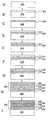
도 1은 본 발명에 기술되는 일 실시예에 따라 유전체 물질을 형성하기 위한 처리 시퀀스를 도시한다.1 shows a processing sequence for forming a dielectric material in accordance with one embodiment described in the present invention.
도 2A-2I는 본 발명에서 기술되는 다른 실시예에 따라 기판 표면 상에 다수의 층들을 증착하기 위한 처리 시퀀스를 도시한다.2A-2I illustrate a processing sequence for depositing multiple layers on a substrate surface in accordance with another embodiment described in the present invention.
*도 3A-3K는 본 발명에서 기술되는 다른 실시예에 따라 기판 표면 상에 다수의 층들을 증착하기 위한 다른 처리 시퀀스를 도시한다.3A-3K illustrate another processing sequence for depositing multiple layers on a substrate surface in accordance with another embodiment described herein.
도 4는 본 발명에서 기술되는 다른 실시예에 따라 유전체 물질을 형성하기 위한 처리 시퀀스를 도시한다.4 shows a processing sequence for forming a dielectric material in accordance with another embodiment described in the present invention.
도 5A-5D는 본 발명에서 기술되는 다른 실시예에 따라 기판 표면 상에 다수의 층들을 형성하기 위한 처리 시퀀스를 도시한다.5A-5D illustrate a processing sequence for forming multiple layers on a substrate surface in accordance with another embodiment described in the present invention.
본 발명의 실시예들은 다양한 애플리케이션들, 특히 트랜지스터와 커패시터 제조에 사용되는 높은 k 유전체 물질들을 위해 사용되는 유전체 물질들을 마련하기 위한 방법들을 제공한다. 원자층 증착(ALD)을 이용하는 프로세스들의 일부는 유전체 화합물들의 원소 조성을 제어한다. 일 실시예에서, 유전체 적층물은 증착 프로세스 동안 유전체 층을 증착하고 그 상부에 질화물 층을 형성하도록 상기 유전체 층을 질화 프로세스에 노출시킴으로써 형성된다. 상기 기판은 시퀀스를 통해 주기적으로 또는 각각의 질화 프로세스 이후 어닐링 프로세스에 노출될 수 있다. 상기 증착, 질화 및 어닐링 프로세스들은 상기 유전체 적층물이 미리 결정된 두께에 도달할 때까지 반복된다.Embodiments of the present invention provide methods for preparing dielectric materials used for a variety of applications, particularly high k dielectric materials used in transistor and capacitor fabrication. Some of the processes using atomic layer deposition (ALD) control the elemental composition of dielectric compounds. In one embodiment, the dielectric stack is formed by depositing a dielectric layer during the deposition process and exposing the dielectric layer to a nitriding process to form a nitride layer thereon. The substrate may be exposed to the annealing process periodically or after each nitriding process in sequence. The deposition, nitriding and annealing processes are repeated until the dielectric stack reaches a predetermined thickness.
유전체 층들은 일반적으로 금속 산화물이고, ALD 프로세스, 종래의 화학적 기상 증착(CVD) 프로세스 또는 물리적 기상 증착(PVD) 프로세스에 의해 증착될 수 있다. 일 예에서, 유전체 층은 실리콘이 실질적으로 없는 금속 산화물이다. 유전체 층들은 하프늄, 탄탈, 티타늄, 알루미늄, 지르코늄, 란탄, 실리콘 또는 이들의 조합물들과 같은 적어도 하나의 부가 엘리먼트와 산소를 포함할 수 있다. 일부 예들에서, 유전체 층들은 하프늄 산화물, 하프늄 실리케이트, 탄탈 산화물, 알루미늄 산화물, 알루미늄 실리케이트, 실리콘 산화물, 이들의 유도체들 또는 이들의 조합물들을 포함한다.The dielectric layers are generally metal oxides and may be deposited by an ALD process, conventional chemical vapor deposition (CVD) process, or physical vapor deposition (PVD) process. In one example, the dielectric layer is a metal oxide that is substantially free of silicon. The dielectric layers may include oxygen and at least one additional element, such as hafnium, tantalum, titanium, aluminum, zirconium, lanthanum, silicon, or combinations thereof. In some examples, the dielectric layers include hafnium oxide, hafnium silicate, tantalum oxide, aluminum oxide, aluminum silicate, silicon oxide, derivatives thereof, or combinations thereof.
다층 유전체 물질의 질소 안정화Nitrogen Stabilization of Multilayer Dielectric Materials
도 1은 하프늄 실리콘 옥시니트라이드 물질과 같은 유전체 물질을 형성하기 위한 예시적인 프로세스(100)를 도시한다. 도 2A-3K는 트랜지스터 및/또는 커패시터와 같은 반도체 소자에 사용되는 유전체 물질의 형성을 도시하기 위한 프로세스(100)에 해당한다. 동일하거나 유사한 조성의 다수의 유전체 층들이 순차적으로 증착되어 유전체 물질을 형성한다. 각각의 유전체 층은 비정질 층 또는 나노결정형 물질을 포함한 층의 형태로 증착된다. 상기 형태는 층 두께가 본질적으로 물질의 치수적인 제한을 초래하기 때문에 각각의 개별 층의 두께에 의존한다. 상기 제한이 작다면, 즉 층 두게가 충분히 얇다면, 층은 비정질 상태로 남을 수 있다.1 shows an
프로세스(100)의 일 실시예에서, 유전체 층(202)은 단계(102)에서, 도 2A-2B에 도시된 것처럼, ALD, CVD, PVD, 열 기술들 또는 이들의 조합들과 같은 종래의 증착 기술들에 의해 기판(200)상에 증착된다. 바람직한 실시예에서, 유전체 층(202)은 본 발명에 참조로 포함되는 "Atomic Layer Deposition of Hafnium-containing High-K Materials"란 명칭으로 2004년 5월 12일자 제출된 어플라이드 머티어리얼스 사의 계류 중인 미국 가특허출원 일련번호 60/570,173호에 기술된 것처럼, ALD 프로세스 및 장치에 의해 증착될 수 있다. 유전체 층(202)은 일반적으로 약 1Å 내지 약 50Å의 막 두께, 바람직하게는 약 5Å 내지 약 30Å, 보다 바람직하게는 약 5Å 내지 약 20Å, 예를 들어 약 15Å의 막 두께로 증착된다.In one embodiment of
유전체 층(202)을 증착하기 이전에, 기판(200)은 다양한 기능 그룹들을 갖는 기판 표면을 제거하기 위해 전처리 프로세스에 노출될 수 있다. 본 발명에서 기술되는 바와 같이 증착 프로세스를 개시하기 이전에 유용한 기능 그룹들은 히드록실(OH), 알콕시(OR, 여기서 R=Me, Et, Pr 또는 Bu), 할옥실(OX, 여기서 X=F, Cl, Br 또는 I), 할라이드(F, Cl, Br 또는 I), 산소 라디칼들, 아미노들(NH 또는 NH2) 및 아미도(NR 또는 NR2, 여기서 R=H, Me, Et, Pr 또는 Bu)를 포함한다. 전처리 프로세스는 NH3, B2H6, SiH4, SiH6, H2O, HF, HCl, O2, O3, H2O, H2O2, H2, 원자-H, 원자-N, 원자-O, 알코올 또는 아민과 같은 반응물에 상기 기판을 노출시킬 수 있다. 상기 기능 그룹들은 기판 표면상에 부착되도록 유입되는 화학적 프로커서를 위한 베이스를 제공할 수 있다. 전처리 프로세스는 약 2초 내지 약 2분, 바람직하게는 약 10초 내지 약 30초 범위의 주기 동안 반응물에 상기 기판 표면을 노출시킬 수 있다. 일 예에서, 기판 표면은 ALD 프로세스를 개시하기 이전에 약 15초 동안 WVG 시스템으로부터 유도되는 수증기에 노출된다.Prior to depositing the
유전체 층(202)은 일반적으로 높은 k 유전체 물질이고, 하프늄, 지르코늄, 티타늄, 탄탈, 란탄, 알루미늄, 실리콘, 산소 및/또는 질소의 조합물들을 포함한다. 유전체 층(202)은 하프늄 산화물들(HfOX 또는 HfO2), 하프늄 실리케이트들(HfSixOy 또는 HfSiO4), 하프늄 실리콘 옥시니트라이드(HfSixOyNz), 하프늄 옥시니트라이드(HfOxNy), 하프늄 알루미네이트들(HfAlxOy), 하프늄 알루미늄 실리케이트들(HfAlxSiyOz), 하프늄 알루미늄 실리콘 옥시니트라이드들(HfAlwSixOyNz), 하프늄 란탄 산화물들(HfLaxOy)과 같은 하프늄 함유 물질들, 지르코늄 산화물들(ZrOX 또는 ZrO2), 지르코늄 실리케이트들(ZrSixOy), 지르코늄 실리콘 옥시니트라이드(ZrSixOyNz), 지르코늄 옥시니트라이드(ZrOxNy), 지르코늄 알루미네이트들(ZrAlxOy), 지르코늄 알루미늄 실리케이트들(ZrAlxSiyOz), 지르코늄 알루미늄 실리콘 옥시니트라이드(ZrAlwSixOyNz), 지르코늄 란탄 산화물(ZrLaxOy)과 같은 지르코늄-함유 물질들, 알루미늄 산화물(Al2O3 또는 AlOx), 알루미늄 옥시니트라이드들(AlOxNy), 알루미늄 실리케이트(AlSixOy), 알루미늄 실리콘 옥시니트라이드(AlSixOyNz), 란탄 알루미늄 산화물(LaAlxOy), 란탄 산화물들(LaOx 또는 La2O3)과 같은 다른 알루미늄-함유 물질들 또는 란탄-함유 물질들, 이들의 유도체들 또는 이들의 조합물들을 포함하는 조성물을 가질 수 있다. 유전체 층(202)을 위해 유용한 다른 유전체 물질들은 티타늄 산화물들(TiOX 또는 TiO2), 티타늄 옥시니트라이드들(TiOxNy), 탄탈 산화물들(TaOx 또는 Ta2O5) 및 탄탈 옥시니트라이드(TaOxNy)를 포함할 수 있다.
단계(104)에서, 유전체 층(202)은 도 2C에 도시된 것처럼, 질소-함유 유전체 층(204)을 형성하도록 질소 원자들을 유전체 물질에 물리적으로 포함시키는 질화 프로세스에 노출된다. 질화 프로세스는 유전체 층 증착 동안(예, ALD 또는 CVD 프로세스들 동안), 디커플링된 플라즈마 질화(DPN), 원격 플라즈마 질화, 핫-와이어 유도 원자-N, 및 질소 삽입을 포함할 수 있다. 질소-함유 유전체 층(204)은 표면에서 일반적으로 질소가 풍부하다. 질소-함유 유전체 층(204)의 질소 농도는 약 5 at% 내지 약 40 at%, 바람직하게는 약 10 at% 내지 약 25 at% 범위일 수 있다. 바람직하게는, 질화 프로세스는 DPN 프로세스와 같이 질소 플라즈마에 유전체 층(202)을 노출시킨다.In
일 실시예에서, 기판은 캘리포니아, 산타 클레라에 위치한 어플라이드 머티어리얼스 사로부터 이용가능한 CENTURA™ DPN 챔버와 같은 DPN 챔버로 수송된다. 일 실시예에서, DPN 챔버는 유전체 층(202)을 증착시키는데 사용되는 ALD 챔버와 동일한 클러스터 툴 상에 있다. 따라서, 기판은 주변 환경에 노출됨이 없이 질화 프로세스에 노출될 수 있다. DPN 프로세스 동안, 유전체 층(202)은 동시-유입 N2 및 이르곤과 같은 희가스 플라즈마에 의해 형성되는 원자-N과 충돌된다. N2 뿐만 아니라, 다른 질소-함유 가스들이 NH3, 히드라진(예, N2H4 또는 MeN2H3), 아민(예, Me3N, Me2NH 또는 MeNH2), 아닐린(예, C6H5NH2) 및 아지드(예, MeN3 또는 Me3SiN3)를 형성하는데 사용될 수 있다. 플라즈마 처리에 사용될 수 있는 다른 희가스들은 헬륨, 네온 및 제논을 포함한다. 질화 프로세스는 약 10초 내지 약 120초, 바람직하게는 약 15초 내지 약 60초의 시간 주기에서 진행되고, 예를 들어 약 30초 동안 진행된다. 또한, 질화 프로세스는 약 900와트 내지 약 2,700와트로 설정되는 플라즈마 전력 및 약 10 mTorr 내지 약 100 mTorr의 압력에서 수행된다. 질소는 약 0.1 slm 내지 약 1.0 slm의 흐름을 갖고, 희가스는 약 0.1 slm 내지 약 1.0 slm의 흐름을 갖는다. 바람직한 실시예에서, 질화 프로세스는 DPN 프로세스이고, 동시에 유동되는 아르곤과 질소에 의한 플라즈마를 포함한다.In one embodiment, the substrate is transported to a DPN chamber, such as the CENTURA ™ DPN chamber available from Applied Materials, Inc., located in Santa Clara, California. In one embodiment, the DPN chamber is on the same cluster tool as the ALD chamber used to deposit the
다른 실시예에서, DPN 챔버에 기판을 수송하는 대신, 질화 프로세스는 유전체 층(202)이 증착되는 동일한 증착 챔버에서 질소 플라즈마에 유전체 층(202)을 노출시키는 단계를 포함할 수 있다. 예를 들어, 질화 원격 플라즈마는 ALD 챔버 또는 CVD 챔버와 같은 원격-플라즈마 장치로 구성되는 처리 챔버에서 질소-함유 유전체 층(204)을 직접 형성하기 위해 유전체 층(202)에 노출된다. 또한, 라디칼 질소 화합물들이 가열 또는 핫-와이어들(hot-wires)에 의해 형성되고 질화 프로세스들 동안 사용될 수 있다. 질소-함유 유전체 층(204)을 형성하면서 ALD 사이클 내에서 부가적인 하프(half) 반응에 질소 프리커서를 포함하면서 및/또는 질소-함유 환경에서 기판의 어닐링과 같은 질소-함유 유전체 층(204)을 형성하기 위한 다른 질화 프로세스들이 고려된다. 예를 들어, 하프늄 실리케이트를 형성하기 위해 ALD 사이클 동안 부가적인 하프 반응은 NH3 펄스 이후 후속되는 정화 가스의 펄스를 포함할 수 있다.In another embodiment, instead of transporting the substrate to the DPN chamber, the nitriding process may include exposing the
도 2A-2I에 도시된 일 실시예에서, 선택적인 어닐링 처리는 단계(106) 동안 생략된다. 단계(108)에서, 유전체 물질의 미리 결정된 두께가 결정된다. 단계들(102-106)의 1 사이클 이후 유전체 물질의 미리 결정된 두께가 달성되면, 프로세스(100)는 단계(110)에서 선택적인 어닐링 프로세스를 지속할 수 있고, 프로세스(100)는 단계(112)에서 종료된다. 그러나, 바람직한 실시예에서, 유전체 물질 두께는 단계들(102-106)의 단지 1사이클 이후 달성되지 않으므로, 단계(102)에서 개시됨으로써 반복된다.In one embodiment shown in FIGS. 2A-2I, the optional annealing process is omitted during
도 2D에서, 유전체 층(212)은 단계(102)에서 논의된 바와 동일한 프로세스에 의해 질소-함유 유전체 층(204) 상에 증착된다. 유전체 층(212)의 층 두께는 유전체 층(202)과 동일한 두께일 필요는 없고 일반적으로 유사한 두께들을 갖는다. 도 2E에서, 유전체 층(212)은 질소-함유 유전체 층(214)을 형성하기 위해 단계(104)에서 논의된 바와 같은 질화 프로세스에 노출된다. 도 2F에서, 유전체 층(222)은 단계(102)에서 논의된 것과 동일한 프로세스에 의해 질소-함유 유전체 층(214) 상에 증착된다. 도 2E에서, 유전체 층(222)은 질소-함유 유전체 층(224)을 형성하도록 단계(104)에서 논의된 바와 같은 질화 프로세스에 노출된다. 단계들(102-106)은 유전체 물질의 미리 결정된 두께를 형성하도록 반복될 수 있다.In FIG. 2D,
도 2H는 단계들(102-106)이 6번 수행된 이후 질소-함유 유전체 층들(204, 214, 224, 234, 244, 254)의 적층물(260)을 도시한다. 그 이후, 유전체 물질의 미리 결정된 두께가 단계(108) 동안 달성되면, 기판은 단계(110) 동안 선택적인 어닐링 프로세스에 노출된다. 기판은 캘리포니아, 산타클레라에 위치한 어플라이드 머티어리얼스 사로부터 이용가능한 CENTURA™ RADIANCE™ RTP 챔버와 같은 어닐링 챔버로 수송되고 어닐링 프로세스에 노출된다. 어닐링 챔버는 증착 챔버 및/또는 질화 챔버와 동일한 클러스터 툴 상에 있을 수 있다. 따라서, 기판은 주위 환경에 노출됨이 없이 어닐링될 수 있다. 기판은 약 1초 내지 약 120초의 시간 주기 동안 약 600℃ 내지 약 1200℃의 온도에서, 예를 들어 약 15초 동안 약 1000℃에서 유지된다. 일반적으로, 처리 챔버 분위기는 O2, N2, NH3, N2H4, NO, N2O 또는 이들의 조합물들과 같은 적어도 하나의 어닐링 가스를 포함한다. 상기 챔버는 약 1 Torr 내지 약 100 Torr의 압력에서, 예를 들어 약 5 Torr의 압력에서 유지된다.2H shows the
어닐링 프로세스는 도 2I에 도시된 것처럼, 유전체 질화물 물질층들(206, 216, 226, 236, 246, 256)을 포함하는 유전체 물질 또는 적층물(270)로 적층물(260)을 변환한다. 어닐링 프로세스는 단계(104) 동안 플라즈마 충돌에 의해 야기되는 임의의 손상을 보수하고, 유전체 질화물 층들의 고정된 전하를 감소시킨다. 유전체 질화물 물질층들(206, 216, 226, 236, 246, 256)은 각각 약 1Å 내지 약 50Å, 바람직하게는 약 5Å 내지 약 30Å, 보다 바람직하게는 약 5Å 내지 약 20Å, 예를 들어 약 15Å의 막 두께를 가질 수 있다. 유전체 물질 또는 적층물(270)은 일반적으로 약 10Å 내지 약 250Å, 바람직하게는 약 20Å 내지 약 100Å, 예를 들어 약 60Å의 두께를 갖는다. 일 실시예에서, 유전체 물질 또는 적층물(270)은 60Å 이하의 두께를 갖는다.The annealing process converts the
프로세스(100)의 다른 실시예에서, 유전체 층(302)은 도 3A-3B에 도시된 것처럼, ALD, 화학적 기상 증착(CVD), 물리적 기상 증착(PVD), 열 기술들 또는 이들의 조합들과 같은 종래의 증착 기술들에 의해 단계(102)에서 기판(300) 상에 증착된다. 바람직한 실시예에서, 유전체 층(302)은 유전체 층(202)에 대해 상술된 것처럼, ALD 프로세스에 의해 증착된다. 유전체 층(302)은 일반적으로 높은 k 유전체 물질이고, 하프늄, 지르코늄, 티타늄, 탄탈, 란탄, 알루미늄, 실리콘, 산소 및/또는 질소의 조합물을 포함한다. 유전체 층(302)은 상술된 것처럼, 유전체 층(202)과 동일한 조성을 가질 수 있다. 유전체 층(302)은 일반적으로 약 1Å 내지 약 50Å, 바람직하게는 약 5Å 내지 약 30Å, 보다 바람직하게는 약 5Å 내지 약 20Å, 예를 들어 약 15Å의 막 두께로 증착된다.In another embodiment of
단계(104)에서, 유전체 층(302)이 도 3C에 도시된 것처럼, 질소-함유 유전체 층(304)을 형성하도록 질소 원자들을 유전체 막에 물리적으로 포함시키는 질화 프로세스에 노출된다. 질화 프로세스는 디커플링된 플라즈마 질화(DPN), 원격 플라즈마 질화, 핫-와이어 유도 원자-N, 및 유전체 증착 동안(예, ALD 또는 CVD 프로세스들 동안) 질소 첨가를 포함할 수 있다. 질소-함유 유전체 층(304)은 일반적으로 표면에서 질소가 풍부하다. 질소-함유 유전체 층(304)의 질소 농도는 약 5 at% 내지 약 40 at%, 바람직하게는 약 10 at% 내지 약 25 at% 범위일 수 있다. 바람직하 게는, 질화 프로세스는 DPN 프로세스와 같은 질소 플라즈마에 유전체 층(302)을 노출시킨다.In
일 실시예에서, 기판은 캘리포니아, 산타클레라에 위치한 어플라이드 머티어리얼스 사로부터 이용가능한 CENTURA™ DPN 챔버와 같은 DPN 챔버로 수송된다. 일 실시예에서, DPN 챔버는 유전체 층(302)을 증착하는데 사용되는 ALD 챔버와 동일한 클러스터 툴 상에 있다. 따라서, 기판은 주위 환경에 노출됨이 없이 질화 프로세스에 노출될 수 있다. DPN 프로세스 동안, 유전체 층(302)은 동시 유입되는 N2, 및 아르곤과 같은 희가스 플라즈마에 의해 형성되는 원자-N과 충돌된다. N2와 더불어, 다른 질소-함유 가스들이 NH3, 히드라진(예, N2H4 또는 MeN2H3), 아민(예, Me3N, Me2NH 또는 MeNH2), 아닐린(예, C6H5NH2) 및 아지드(예, MeN3 또는 Me3SiN3)와 같은 질소 플라즈마를 형성하는데 사용될 수 있다. 플라즈마 프로세스에 사용될 수 있는 다른 희가스들은 헬륨, 네온 및 제논을 포함한다. 질화 프로세스는 약 10초 내지 약 120초, 바람직하게는 약 15초 내지 약 60초의 시간 주기에서, 예를 들어 약 30초 동안 진행된다. 또한, 질화 프로세스는 약 900와트 내지 약 2700와트로 설정되는 플라즈마 전력 및 약 10 mTorr 내지 약 100 mTorr의 압력에서 수행된다. 질소는 약 0.1 slm(분당 표준 리터) 내지 약 1.0 slm의 흐름을 갖고, 희가스는 약 0.1 slm 내지 약 1.0 slm의 흐름을 갖는다. 바람직한 실시예에서, 질화 프로세스는 DPN 프로세스이고, 동시 유입되는 Ar 및 N2에 의한 플라즈마를 포함한다.In one embodiment, the substrate is transported to a DPN chamber, such as the CENTURA ™ DPN chamber available from Applied Materials, Inc., located in Santa Clara, California. In one embodiment, the DPN chamber is on the same cluster tool as the ALD chamber used to deposit the
다른 실시예에서, 기판을 DPN 챔버에 수송하는 대신에, 질화 프로세스는 유전체 층(302)이 증착되는 동일한 증착 챔버에서 질소 플라즈마에 유전체 층(302)을 노출시키는 단계를 포함할 수 있다. 예를 들어, 질소 원격-플라즈마는 ALD 챔버 또는 CVD 챔버와 같은 원격-플라즈마 장치로 구성되는 처리 챔버에서 질소-함유 유전체 층(304)을 직접 형성하기 위해 유전체 층(302)에 노출된다. 라디칼 질소 화합물들은 또한 가열 또는 핫-와이어들에 의해 형성될 수 있고 질화 프로세스들 동안 사용될 수 있다. 질소-함유 유전체 층(304)을 형성하면서 ALD 사이클 내에서 부가적인 하프 반응에 질소 프리커서를 포함하면서 및/또는 질소-함유 환경에서 기판의 어닐링과 같은 질소-함유 유전체 층(304)을 형성하기 위한 다른 질화 프로세스들이 고려된다. 예를 들어, 하프늄 실리케이트를 형성하기 위한 ALD 사이클 동안 부가적인 하프 반응은 NH3의 펄스 이후 후속되는 정화 가스의 펄스를 포함할 수 있다.In another embodiment, instead of transporting the substrate to the DPN chamber, the nitriding process may include exposing the
도 3A-3K에 도시된 일 실시예에서, 선택적인 어닐링 프로세스는 단계(106) 동안 실행된다. 기판은 캘리포니아, 산타클레라에 위치한 어플라이드 머티어리얼스 사로부터 이용가능한 CENTURA™ RADIANCE™ RTP 챔버와 같은 어닐링 챔버로 수송되고 어닐링 프로세스에 노출된다. 어닐링 챔버는 증착 챔버 및/또는 질화 챔버와 동일한 클러스터 툴 상에 있을 수 있다. 따라서, 기판은 주위 환경에 노출됨이 없이 어닐링될 수 있다. 기판은 약 1초 내지 약 120초의 시간 주기 동안 약 600℃ 내지 약 1200℃의 온도에서, 예를 들어 약 15초 동안 약 1000℃의 온도에서 유지된 다. 일반적으로, 처리 챔버 분위기는 O2, N2, NH3, N2H4, NO, N2O 또는 이들의 조합물들과 같은 적어도 하나의 어닐링 가스를 포함한다. 상기 챔버는 약 1 Torr 내지 약 100 Torr의 압력에서, 예를 들어 약 5 Torr의 압력에서 유지된다.In one embodiment shown in FIGS. 3A-3K, an optional annealing process is performed during
어닐링 프로세스는 도 3D에 도시된 것처럼, 질소-함유 유전체 층(304)을 유전체 질화물 물질층들(306)로 변환한다. 어닐링 프로세스는 단계(104) 동안 플라즈마 충돌에 의해 야기된 임의의 손상을 수리하고 질소-함유 유전체 층(304)의 고정된 전하를 감소시킨다. 단계(108)에서, 미리 결정된 두께의 유전체 물질이 결정된다. 단계들(102-106)의 1 사이클 이후, 미리 결정된 층 두께의 유전체 물질이 달성되면, 단계(100)는 단계(110) 동안 선택적인 어닐링 프로세스를 생략하고 단계(112) 동안 종료된다. 그러나, 바람직한 실시예에서, 유전체 물질 두께는 단계들(102-106)의 단지 1 사이클 이후에 달성되지 않으므로, 반복된다.The annealing process converts the nitrogen-containing
도 3E에서, 유전체 층(312)은 단계(102)에서 논의된 것과 동일한 프로세스에 의해 유전체 질화물 층(306) 상에 증착된다. 유전체 층(312)의 층 두께는 유전체 층(302)과 동일한 두께일 필요는 없지만, 일반적으로 유사한 두께들을 갖는다. 도 3F에서, 유전체 층(312)은 질소-함유 유전체 층(314)을 형성하기 위해 단계(104)에서 논의된 바와 같은 질화 프로세스에 노출된다. 도 3G에서, 기판은 질소-함유 유전체 층(314)을 유전체 질화물 층(316)으로 변환하도록 단계(106)에서 논의된 바와 같은 어닐링 프로세스에 노출된다. 도 3H에서, 유전체 층(322)은 단계(102)에서 논의된 것과 동일한 프로세스에 의해 유전체 질화물 층(316) 상에 증착된다. 도 3I에서, 유전체 층(322)은 질소-함유 유전체 층(324)을 형성하도록 단계(104)에서 논의된 바와 같은 질화 프로세스에 노출된다. 도 3J에서, 기판은 질소-함유 유전체 층(324)을 유전체 질화물 층(326)으로 변환하도록 단계(106)에서 어닐링 프로세스에 노출된다. 단계들(102-106)은 유전체 물질의 미리 결정된 두께를 형성하도록 반복될 수 있다.In FIG. 3E,
도 3K는 단계들(102-106)이 6번 수행된 이후 유전체 질화물 물질층들(306, 316, 326, 336, 346, 356)의 적층물(370) 또는 유전체 물질을 도시한다. 유전체 질화물 물질층들(306, 316, 326, 336, 346, 356)은 각각 약 1Å 내지 약 50Å, 바람직하게는 약 5Å 내지 약 30Å, 보다 바람직하게는 약 5Å 내지 약 20Å, 예를 들어 약 15Å의 막 두께를 가질 수 있다. 유전체 물질 또는 적층물(370)은 일반적으로 약 10Å 내지 약 250Å, 바람직하게는 약 20Å 내지 약 100Å, 예를 들어 60Å의 두께를 갖는다. 일 실시예에서, 유전체 물질 또는 적층물(370)은 약 60Å 이하의 두께를 갖는다.3K shows a
도 2I 및 3K는 6개의 유전체 질화물 물질층들을 포함하는 적층물들(270, 370)을 도시하지만, 많은 층들이 유전체 물질을 형성하기 위해 증착될 수 있다. 유전체 물질은 2개만큼 적은 층들 또는 수백개의 층들을 가질 수 있다. 예를 들어, 약 60Å의 전체 두께들로 형성되는 유전체 물질은 다른 것들 중에서 12개의 5Å 유전체 층들, 6개의 10Å 유전체 층들, 4개의 15Å 유전체층들, 3개의 20Å 유전체 층들 또는 2개의 30Å 유전체 층들을 포함할 수 있다. 다른 예에서, 약 100Å의 전체 두께로 형성되는 유전체 물질은 다른 것들 중에서 20개의 5Å 유전체 층 들, 10개의 10Å 유전체 층들, 5개의 20Å 유전체 층들, 4개의 25Å 유전체 층들 또는 2개의 50Å 유전체 층들을 포함할 수 있다. 유전체 물질은 비정질 상태로 남아 있고, 약 5 at% 내지 약 25 at%, 바람직하게는 약 10 at% 내지 약 20 at% 범위, 예를 들어 약 15 at%의 질소 농도를 가질 수 있다.2I and
전술한 것처럼, 유전체 물질 또는 적층물(270)은 목표된 수의 유전체 층들이 증착된 이후 또는 미리 결정된 막 두께가 달성된 이후 기판을 어닐링함으로써 형성된다. 선택적으로, 유전체 물질 또는 적층물(370)은 유전체 층들의 각각의 질화 이후 기판을 어닐링함으로써 달성된다. 다른 실시예에서, 단계(106)의 선택적인 어닐링 프로세스는 단계들(102-106)의 사이클 동안 제공될 수 있고 유전체 물질의 형성 동안 단계들(102-106)의 다른 사이클 동안 생략될 수 있다. 기판을 어닐링 프로세스에 노출시키는 정확한 간격들을 결정하기 위해 루틴 실험이 수행될 수 있다. 어닐링 간격들을 유도하는 몇몇 변수들은 질화 프로세스 동안 사용되는 특정 질화 기술, 유전체 층들의 두께와 조성, 및 최종 유전체 물질의 목표된 특성들을 포함한다.As mentioned above, the dielectric material or stack 270 is formed by annealing the substrate after the desired number of dielectric layers have been deposited or after a predetermined film thickness has been achieved. Optionally, the dielectric material or stack 370 is achieved by annealing the substrate after each nitriding of the dielectric layers. In other embodiments, the optional annealing process of
유전체 물질의 질소 안정화Nitrogen Stabilization of Dielectric Materials
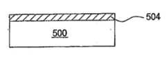
도 4는 하프늄 옥시니트라이드 물질 또는 탄탈 옥시니트라이드 물질과 같은 유전체 물질을 형성하기 위한 예시적인 프로세스(400)를 도시한다. 도 5A-5D는 트랜지스터 및/또는 커패시터와 같은 반도체 소자에 사용되는 유전체 물질의 형성을 도시하는 프로세스(400)에 해당한다. 기판(500) 상에 배치된 유전체 층(502)은 질소-함유 유전체 층(504)을 형성하기 위한 질화 프로세스에 노출된다. 순차적으로, 질소-함유 유전체 층(504)은 어닐링 프로세스에 대한 노출에 의해 유전체 질화물 유전체 층(506)으로 변환된다.4 shows an
프로세스(400)의 일 실시예에서, 유전체 층(502)은 도 5A-5B에 도시된 것처럼, ALD, CVD, PVD, 열 기술들 또는 이들의 조합들과 같은 종래의 증착 기술들에 의해 단계(402) 동안 기판(500) 상에 증착된다. 바람직한 실시예에서, 유전체 층(502)은 본 발명에 참조로 포함되는 어플라이드 머티어리얼스 사의 "Atomic Layer Deposition of Hafnium-containing High-K Materials"란 명칭으로 2004년 5월 12일자로 제출된 공동 계류중인 미국 가특허출원에 기술된 것처럼, ALD 프로세스 및 장치에 의해 증착된다. 유전체 층(502)은 일반적으로 약 5Å 내지 약 300Å, 바람직하게는 약 10Å 내지 약 200Å, 보다 바람직하게는 약 10Å 내지 약 100Å, 예를 들어 약 50Å의 막 두께로 증착된다.In one embodiment of
기판은 히드록실(OH), 알콕시(OR, 여기서 R= Me, Et, Pr 또는 Bu), 할옥실(OX, 여기서 X=F, Cl, Br 또는 I), 할라이드(F, Cl, Br 또는 I), 산소 라디칼들, 아미노(NH 또는 NH2) 및 아미도들(NR 또는 NR2, 여기서 R=H, Me, Et, Pr 또는 Bu)과 같은 다양한 기능 그룹들을 가진 종단부를 갖도록 하기 위해 유전체 층(502)을 증착하기 이전에 전처리될 수 있다. 전처리는 ALD 프로세스 또는 CVD 프로세스로 유전체 층(502)을 증착하기 이전에 특히 유용하다. 전처리는 NH3, B2H6, SiH4, Si2H6, H2O, HF, HCl, O2, O3, H2O, H2O/O2, H2O/H2, H2O2, H2, 원자-H, 원자-N, 원자-O, 알코올 또는 아민과 같은 반응물을 투여함으로써 영향을 받을 수 있다. 기판의 표면이 전처리되면, ALD 사이클이 개시된다. 많은 높은 k 유전체 물질들에 대해, 프리커서 흡수는 특정 처리 조건들하에서 자체-제한되고, 일반적으로 이러한 상태를 나타내는 저온들(<300℃)에 있다. 일 실시예에서, 전처리는 하프늄 화합물을 증착하기 이전에 반응물을 통한 사전-침수(presoak)를 포함할 수 있다. 사전-침수는 약 5초 내지 약 120초, 바람직하게는 약 5초 내지 약 30초의 시간 주기 동안 반응물에 기판 표면을 노출시키는 단계를 포함할 수 있다. 일 예에서, 기판 표면은 유전체 층(502)을 증착하기 위한 ALD 프로세스를 개시하기 이전에 약 15초 동안 물에 노출된다.Substrates include hydroxyl (OH), alkoxy (OR where R = Me, Et, Pr or Bu), haloxyl (OX, where X = F, Cl, Br or I), halide (F, Cl, Br or I ), Dielectric layer to have terminations with various functional groups such as oxygen radicals, amino (NH or NH2 ) and amidos (NR or NR2 , where R = H, Me, Et, Pr or Bu) It may be pretreated prior to depositing 502. Pretreatment is particularly useful prior to depositing
유전체 층(502)은 기판 표면 상에 증착되고, 균질적, 이질적, 단계적 및/또는 다층의 적층물들 또는 라미네이트들인 다양한 조성물들을 가질 수 있다. 유전체 층(502)은 일반적으로 높은 k 유전체 물질이고, 하프늄, 지르코늄, 티타늄, 탄탈, 란탄, 알루미늄, 산소 및/또는 질소의 조합물들을 포함한다. 금속 산화물 또는 금속 옥시니트라이드는 유전체 층(502)으로서 사용된다. 유전체 층(502)으로 실리콘의 일부 확산이 기판으로부터 발생할 수 있지만, 유전체 층(502)에는 일반적으로 실리콘이 실질적으로 없다. 유전체 층(502)은 하프늄 산화물들(HfOX 또는 HfO2), 하프늄 옥시니트라이드(HfOxNy), 하프늄 알루미네이트들(HfAlxOy), 하프늄 란탄 산화물들(HfLaxOy)과 같은 하프늄 함유 물질들, 지르코늄 산화물들(ZrOX 또는 ZrO2), 지르코늄 옥시니트라이드(ZrOxNy), 지르코늄 알루미네이트들(ZrAlxOy), 지르 코늄 란탄 산화물(ZrLaxOy)과 같은 지르코늄-함유 물질들, 알루미늄 산화물(Al2O3 또는 AlOx), 알루미늄 옥시니트라이드들(AlOxNy), 란탄 알루미늄 산화물(LaAlxOy), 란탄 산화물들(LaOx 또는 La2O3)과 같은 다른 알루미늄-함유 물질들 또는 란탄-함유 물질들, 이들의 유도체들 또는 이들의 조합물들을 포함하는 조성물을 가질 수 있다. 유전체 층(502)을 위해 유용한 다른 유전체 물질들은 티타늄 산화물들(TiOX 또는 TiO2), 티타늄 옥시니트라이드들(TiOxNy), 탄탈 산화물들(TaOx 또는 Ta2O5) 및 탄탈 옥시니트라이드(TaOxNy)를 포함할 수 있다. 유전체 층(502)을 위해 유용한 유전체 물질들인 적층 막들은 HfO2/Al2O3, La2O3/Al2O3 및 HfO2/La2O3/Al2O3를 포함한다.
단계(404)에서, 유전체 층(502)은 도 5C에 도시된 것처럼, 질소-함유 유전체 층(504)을 형성하도록 질소 원자들을 유전체에 물리적으로 포함시키는 질화 프로세스에 노출된다. 질화 프로세스는 디커플링된 플라즈마 질화(DPN), 원격 플라즈마 질화, 핫-와이어 유도 원자-N, 및 유전체 증착 동안(예, ALD 또는 CVD 프로세스들 동안) 질소 첨가를 포함할 수 있다. 질소-함유 유전체 층(504)은 일반적으로 표면에서 질소가 풍부하다. 질소-함유 유전체 층(504)의 질소 농도는 약 5 at% 내지 약 40 at%, 바람직하게는 약 10 at% 내지 약 25 at% 범위일 수 있다. 바람직하게는, 질화 프로세스는 DPN 프로세스와 같은 질소 플라즈마에 유전체 층(502)을 노출시킨다.In
일 실시예에서, 기판은 캘리포니아, 산타클레라에 위치한 어플라이드 머티어 리얼스 사로부터 이용가능한 CENTURA™ DPN 챔버와 같은 DPN 챔버로 수송된다. 일 실시예에서, DPN 챔버는 유전체 층(502)을 증착하는데 사용되는 ALD 챔버와 동일한 클러스터 툴 상에 있다. 따라서, 기판은 주위 환경에 노출됨이 없이 질화 프로세스에 노출될 수 있다. DPN 프로세스 동안, 유전체 층(502)은 동시 유입되는 N2, 및 아르곤과 같은 희가스 플라즈마에 의해 형성되는 원자-N과 충돌된다. N2와 더불어, 다른 질소-함유 가스들이 NH3, 히드라진(예, N2H4 또는 MeN2H3), 아민(예, Me3N, Me2NH 또는 MeNH2), 아닐린(예, C6H5NH2) 및 아지드(예, MeN3 또는 Me3SiN3)와 같은 질소 플라즈마를 형성하는데 사용될 수 있다. 플라즈마 프로세스에 사용될 수 있는 다른 희가스들은 헬륨, 네온 및 제논을 포함한다. 질화 프로세스는 약 10초 내지 약 120초, 바람직하게는 약 15초 내지 약 60초의 시간 주기에서, 예를 들어 약 30초 동안 진행된다. 또한, 질화 프로세스는 약 900와트 내지 약 2700와트로 설정되는 플라즈마 전력 및 약 10 mTorr 내지 약 100 mTorr의 압력에서 수행된다. 질소는 약 0.1 slm 내지 약 1.0 slm의 흐름을 갖고, 희가스는 약 0.1 slm 내지 약 1.0 slm의 흐름을 갖는다. 바람직한 실시예에서, 질화 프로세스는 DPN 프로세스이고, 동시 유입되는 Ar 및 N2에 의한 플라즈마를 포함한다.In one embodiment, the substrate is transported to a DPN chamber, such as the CENTURA ™ DPN chamber available from Applied Materials Realty, Inc., located in Santa Clara, California. In one embodiment, the DPN chamber is on the same cluster tool as the ALD chamber used to deposit the
다른 실시예에서, 기판을 DPN 챔버에 수송하는 대신에, 질화 프로세스는 유전체 층(502)이 증착되는 동일한 증착 챔버에서 질소 플라즈마에 유전체 층(502)을 노출시키는 단계를 포함할 수 있다. 예를 들어, 질소 원격-플라즈마는 ALD 챔버 또는 CVD 챔버와 같은 원격-플라즈마 장치로 구성되는 처리 챔버에서 질소-함유 유전체 층(504)을 직접 형성하기 위해 유전체 층(502)에 노출된다. 라디칼 질소 화합물들은 또한 가열 또는 핫-와이어들에 의해 형성될 수 있고 질화 프로세스들 동안 사용될 수 있다. 질소-함유 유전체 층(504)을 형성하면서 ALD 사이클 내에서 부가적인 하프 반응에 질소 프리커서를 포함하는 및/또는 질소-함유 환경에서 기판의 어닐링과 같은 질소-함유 유전체 층(504)을 형성하기 위한 다른 질화 프로세스들이 고려된다. 예를 들어, 하프늄 산화물을 형성하기 위한 ALD 사이클 동안 부가적인 하프 반응은 NH3의 펄스 이후 후속되는 정화 가스의 펄스를 포함할 수 있다.In another embodiment, instead of transporting the substrate to the DPN chamber, the nitriding process may include exposing the
단계(406)에서, 기판은 어닐링 프로세스에 노출된다. 기판은 캘리포니아, 산타클레라에 위치한 어플라이드 머티어리얼스 사로부터 이용가능한 CENTURA™ RADIANCE™ RTP 챔버와 같은 어닐링 챔버로 수송되고 어닐링 프로세스에 노출된다. 어닐링 챔버는 증착 챔버 및/또는 질화 챔버와 동일한 클러스터 툴 상에 있을 수 있다. 따라서, 기판은 주위 환경에 노출됨이 없이 어닐링될 수 있다. 기판은 약 1초 내지 약 120초의 시간 주기 동안 약 600℃ 내지 약 1200℃의 온도에서, 예를 들어 약 60초 동안 약 1000℃의 온도에서 유지된다. 일반적으로, 처리 챔버 분위기는 O2, N2, NH3, N2H4, NO, N2O 또는 이들의 조합물들과 같은 적어도 하나의 어닐링 가스를 포함한다. 상기 챔버는 약 5 Torr 내지 약 100 Torr의 압력에서, 예를 들어 약 5 Torr의 압력에서 유지된다.In
어닐링 프로세스는 도 5D에 도시된 것처럼, 질소-함유 유전체 층(504)을 유 전체 물질 또는 유전체 질화물 층(506)으로 변환한다. 어닐링 프로세스는 단계(404) 동안 플라즈마 충돌에 의해 야기된 임의의 손상을 수리하고 유전체 질화물 층(506)의 고정된 전하를 감소시킨다. 유전체 물질은 비정질 상태로 남아 있고, 약 5 at% 내지 약 25 at%, 바람직하게는 약 10 at% 내지 약 20 at% 범위, 예를 들어 약 15 at%의 질소 농도를 가질 수 있다. 유전체 질화물 층(506)은 약 5Å 내지 약 300Å, 바람직하게는 약 10Å 내지 약 200Å, 보다 바람직하게는 약 10Å 내지 약 100Å, 예를 들어 약 50Å의 막 두께를 갖는다.The annealing process converts the nitrogen-containing
본 발명에서 사용되는 바와 같은 "기판 표면"은 그 상부에 막 처리가 수행되는 기판 상에 형성된 물질 표면 또는 임의의 기판을 지칭한다. 예를 들어, 처리가 수행될 수 있는 기판 표면은 유전체 물질들, 실리콘, 실리콘 산화물, 변형된 실리콘, 절연체 상의 실리콘(SOI), 탄소 도핑된 실리콘 산화물들, 실리콘 질화물, 도핑된 실리콘, 게르마늄, 갈륨 비소, 유리, 사파이어와 같은 물질들, 및 금속들, 금속 질화물들, 금속 합금들과 같은 임의의 다른 물질들, 및 애플리케이션에 따른 다른 전도성 물질들을 포함한다. 기판 표면 상의 배리어 층들, 금속들 또는 금속 질화물들은 티타늄, 티타늄 질화물, 텅스텐 질화물, 탄탈 및 탄탈 질화물을 포함한다. 기판들은 직사각형 또는 정사각형 패인들(panes) 뿐만 아니라 200mm 또는 300mm 직경 웨이퍼들과 같은 다양한 치수들을 가질 수 있다. 본 발명에서 기술된 프로세스들의 실시예들은 많은 기판들 및 표면들, 특히 높은 k 유전체 물질들 상에 실리콘-함유 화합물들을 증착한다. 본 발명의 실시예들에 유용할 수 있는 기판들은 반도체 웨이퍼들에 제한되지 않으며, 결정형 실리콘(예, Si<100> 또는 Si<111>), 실리 콘 산화물, 변형된 실리콘, 실리콘 게르마늄, 도핑된 또는 비도핑된 폴리실리콘, 도핑 또는 비도핑된 실리콘 웨이퍼들, 실리콘 질화물 및 패턴 또는 비패턴 웨이퍼들을 포함한다. 표면들은 베어 실리콘 웨이퍼들, 막들, 층들 및 유전체를 가진 물질들, 전도성 및 배리어 특성들을 포함하고, 알루미늄 산화물 및 폴리실리콘을 포함한다. 표면들의 전처리는 연마, 에칭, 환원, 산화, 수산화, 어닐링 및/또는 가열을 포함한다."Substrate surface" as used in the present invention refers to any substrate or material surface formed on the substrate on which the film treatment is performed. For example, the substrate surface on which the treatment may be performed may include dielectric materials, silicon, silicon oxide, strained silicon, silicon on insulator (SOI), carbon doped silicon oxides, silicon nitride, doped silicon, germanium, gallium Materials such as arsenic, glass, sapphire, and any other materials such as metals, metal nitrides, metal alloys, and other conductive materials depending on the application. Barrier layers, metals or metal nitrides on the substrate surface include titanium, titanium nitride, tungsten nitride, tantalum and tantalum nitride. Substrates can have various dimensions, such as 200 mm or 300 mm diameter wafers, as well as rectangular or square panes. Embodiments of the processes described in this invention deposit silicon-containing compounds on many substrates and surfaces, especially high k dielectric materials. Substrates that may be useful in embodiments of the present invention are not limited to semiconductor wafers, and include crystalline silicon (eg, Si <100> or Si <111>), silicon oxide, modified silicon, silicon germanium, doped Or undoped polysilicon, doped or undoped silicon wafers, silicon nitride and patterned or unpatterned wafers. Surfaces include bare silicon wafers, films, layers and dielectric materials, conductive and barrier properties, and include aluminum oxide and polysilicon. Pretreatment of the surfaces includes polishing, etching, reduction, oxidation, hydroxide, annealing and / or heating.
본 발명에 사용되는 것처럼 "원자층 증착" 또는 "주기적 증착"은 기판 표면 상에 물질층을 증착하기 위한 2개 이상의 반응성 화합물들의 순차적인 유입을 지칭한다. 2개, 3개 또는 그 이상의 반응성 화합물들은 처리 챔버의 반응 영역으로 선택적으로 유입될 수 있다. 일반적으로, 각각의 반응성 화합물은 각각의 화합물이 기판 표면 상에서 부착 및/또는 반응할 수 있도록 시간 지연에 의해 분리된다. 일 실시예에서, 제 1 프리커서 또는 화합물 A는 반응 영역으로 펄스화된 이후 제 1 시간 지연이 후속된다. 그 다음, 제 2 프리커서 또는 화합물 B가 반응 영역에 펄스화된 이후 제 2 지연이 후속된다. 각각의 시간 지연 동안 질소와 같은 정화 가스는 반응 영역을 정화시키거나, 그렇지 않을 경우 반응 영역으로부터 부산물들 또는 임의의 잔류 반응성 화합물을 제거하도록 처리 챔버로 유입된다. 선택적으로, 정화 가스는 증착 프로세스를 통해 연속적으로 유동되어 정화 가스만이 반응성 화합물들의 펄스들 사이의 시간 지연 동안 유동될 수 있다. 반응성 화합물들은 목표된 막 또는 막 두께들이 기판 표면 상에 형성될 때까지 교번으로 펄스화된다. 한가지 시나리오에서, 화합물 A와 정화 가스를 펄스화하는 ALD 프로세스, 화합물 B와 정화 가스를 펄스화하는 ALD 프로세스는 하나의 사이클이다. 하나의 사이클은 화합물 A 또는 화합물 B로 개시될 수 있고, 목표된 두께를 가진 막을 달성할 때까지 사이클의 각 순서를 계속할 수 있다. 다른 실시예에서, 제 1 프리커서 함유 화합물 A, 제 2 프리커서 함유 화합물 B 및 제 3 프리커서 함유 화합물 C는 각각 개별적으로 처리 챔버에 펄스화된다. 선택적으로, 제 1 프리커서의 펄스는 제 3 프리커서의 펄스가 상기 제 1 및 제 2 프리커서의 펄스를 갖는 시간에서 중첩되지 않으면서 제 2 프리커서의 펄스를 갖는 시간에서 중첩될 수 있다.As used herein, "atomic layer deposition" or "periodic deposition" refers to the sequential influx of two or more reactive compounds for depositing a layer of material on a substrate surface. Two, three or more reactive compounds may be selectively introduced into the reaction zone of the treatment chamber. In general, each reactive compound is separated by a time delay so that each compound can attach and / or react on the substrate surface. In one embodiment, the first precursor or Compound A is pulsed into the reaction zone followed by a first time delay. Then, a second delay is followed after the second precursor or compound B is pulsed in the reaction zone. During each time delay, purge gas, such as nitrogen, is introduced into the processing chamber to purify the reaction zone or otherwise remove by-products or any residual reactive compound from the reaction zone. Optionally, the purge gas can be continuously flowed through the deposition process such that only the purge gas can be flowed for a time delay between pulses of reactive compounds. The reactive compounds are alternately pulsed until the desired film or film thicknesses are formed on the substrate surface. In one scenario, an ALD process that pulses Compound A and purge gas, and an ALD process that pulses Compound B and purge gas is one cycle. One cycle can be initiated with Compound A or Compound B and can continue each sequence of cycles until a film with the desired thickness is achieved. In another embodiment, the first precursor containing compound A, the second precursor containing compound B and the third precursor containing compound C are each individually pulsed in the processing chamber. Optionally, the pulses of the first precursor can be superimposed at the time having the pulses of the second precursor without the pulses of the third precursor having overlapping the pulses of the first and second precursors.
본 발명에서 사용되는 것처럼 "펄스"는 처리 챔버의 반응 영역에 단속적으로 또는 비연속적으로 유입되는 특정 화합물의 양을 지칭하는 것으로 의도된다. 각각의 펄스 내에서 특정 화합물의 양은 펄스의 지속주기에 따라 시간에 대해 가변될 수 있다. 각각의 펄스의 지속주기는 예를 들어, 사용되는 처리 챔버의 부피 용량, 이에 결합된 진공 시스템 및 특정 화합물 자체의 휘발성/반응성과 같은 다수의 팩터들에 따라 가변될 수 있다. 본 발명에서 사용되는 바와 같은 "하프-반응"은 프리커서 펄스 단계 이후 후속되는 정화 단계를 지칭하는 것이다.As used herein, "pulse" is intended to refer to the amount of a particular compound that enters the reaction zone of the processing chamber intermittently or discontinuously. The amount of a particular compound in each pulse can vary over time depending on the duration of the pulse. The duration of each pulse can vary depending on a number of factors such as, for example, the volume capacity of the processing chamber used, the vacuum system coupled thereto and the volatility / reactivity of the particular compound itself. As used herein, "half-reaction" refers to a purge step following the precursor pulse step.
예제들Examples
예 1 - 기판이 ALD 챔버에 배치되고 기판 표면은 전처리에 노출되어 히드록실 그룹들을 형성한다. 하프늄 실리케이트 층은 하프늄 프리커서(HfCl4), 실리콘 프리커서(TDMAS), 및 캘리포니아 산타클레라에 위치한 Fujukin of Amerixa, Inc.로부터 이용가능한 수증기 생성기(WVG) 시스템에 의해 형성되는 인-시튜 수증기를 이 용하는 ALD 프로세스를 수행함으로써 기판 표면 상에 증착된다. ALD 사이클은 질소 정화 사이클과 분리된 각각의 프리커서를 갖는 HfCl4, 수증기, TDMAS 및 수증기를 순차적으로 펄스화하는 단계를 포함한다. ALD 사이클은 약 4Å의 두께를 갖는 하프늄 실리케이트 층을 형성하기 위해 10번 반복된다.Example 1-A substrate is placed in an ALD chamber and the substrate surface is exposed to pretreatment to form hydroxyl groups. The hafnium silicate layer contains in-situ water vapor formed by hafnium precursor (HfCl4 ), silicon precursor (TDMAS), and a vapor generator (WVG) system available from Fujukin of Amerixa, Inc., located in Santa Clara, California. This solution is deposited on the substrate surface by performing an ALD process. The ALD cycle includes sequentially sequencing HfCl4 , water vapor, TDMAS, and water vapor with respective precursors separated from the nitrogen purge cycle. The ALD cycle is repeated 10 times to form a hafnium silicate layer having a thickness of about 4 ms.
기판은 캘리포니아 산타클레라에 위치한 어플라이드 머티어리얼스 사로부터 이용가능한 CENTURA™ DPN 챔버와 같은 디커플링된 플라즈마 질화(DPN) 챔버로 수송된다. 기판 표면은 아르곤 플라즈마와 동시 유입되는 N2에 의한 질화 프로세스에 노출된다. 질화 프로세스는 하프늄 실리케이트 층 내에 질소 원자들을 포함시키기 위해 약 10초 동안 진행된다. 기판은 캘리포니아, 산타클레라에 위치한 어플라이드 머티어리얼스 사로부터 이용가능한 CENTURA™ RADIANCE™ RTP 챔버와 같은 어닐링 챔버로 수송되고 어닐링 프로세스에 노출된다. 기판은 약 15 Torr에서 유지되는 O2 분위기에서 약 15초 동안 약 1000℃에서 유지된다. 첨가된 질소 원자들은 하프늄 실리콘 옥시니트라이드를 형성하기 위해 하프늄 실리케이트와 결합들을 형성한다. ALD 프로세스, 질화 프로세스 및 어닐링 프로세스를 포함하는 프로세스 사이클은 약 60Å의 두께를 가진 하프늄 실리콘 옥시니트라이드 층을 형성하도록 15번 반복된다.The substrate is transported to a decoupled plasma nitridation (DPN) chamber, such as the CENTURA ™ DPN chamber, available from Applied Materials, Inc. of Santa Clara, California. The substrate surface is exposed to a nitriding process by N2 which co-flows with the argon plasma. The nitriding process proceeds for about 10 seconds to include nitrogen atoms in the hafnium silicate layer. The substrate is transported to an annealing process and exposed to an annealing process, such as the CENTURA ™ RADIANCE ™ RTP chamber, available from Applied Materials, Inc. of Santa Clara, California. The substrate is held at about 1000 ° C. for about 15 seconds in an O2 atmosphere maintained at about 15 Torr. The added nitrogen atoms form bonds with hafnium silicate to form hafnium silicon oxynitride. The process cycle, including the ALD process, nitriding process, and annealing process, was repeated 15 times to form a hafnium silicon oxynitride layer with a thickness of about 60 ms.
예 2 - 기판은 원격 플라즈마 생성기가 구비된 ALD 챔버에 배치되고 기판 표면은 히드록실 그룹들을 형성하도록 전처리에 노출된다. 하프늄 실리케이트 층은 하프늄 프리커서(TDEAH), 실리콘 프리커서(Tris-DMAS), 및 캘리포니아 산타클레라 에 위치한 Fujikin of America, Inc.로부터 이용가능한 수증기 생성기(WVG) 시스템에 의해 생성되는 인-시튜 수증기를 이용하는 ALD 프로세스를 수행함으로써 기판 표면 상에 증착된다. ALD 사이클은 제 1 하프 반응에서 TDEAH 및 Tris-DMAS를 동시 유동시키는 단계, 및 제 2 하프 반응에서 수증기를 순차적으로 펄스화하는 단계를 포함하고, 각각의 하프 반응은 아르곤 정화에 의해 분리된다. 하프늄 실리케이트 층은 막이 약 4Å의 두께를 가질 때까지 사이클을 10번 반복함으로써 형성된다.Example 2 A substrate is placed in an ALD chamber equipped with a remote plasma generator and the substrate surface is exposed to pretreatment to form hydroxyl groups. The hafnium silicate layer is in-situ vapor produced by a hafnium precursor (TDEAH), silicon precursor (Tris-DMAS), and a vapor generator (WVG) system available from Fujikin of America, Inc., located in Santa Clara, California. Deposited on the substrate surface by performing an ALD process. The ALD cycle includes co-flowing TDEAH and Tris-DMAS in the first half reaction, and sequentially pulsed water vapor in the second half reaction, each half reaction being separated by argon purification. The hafnium silicate layer is formed by repeating the cycle ten times until the film has a thickness of about 4 mm 3.
ALD 프로세스는 중지되고 기판은 원격 플라즈마 생성기가 구비된 ALD 챔버에서 유지된다. 기판 표면은 하프늄 실리케이트 층내에 질소 원자들을 포함시키기 위해 약 10초 동안 원격 플라즈마 질화 프로세스에 노출된다. 기판은 캘리포니아 산타클레라에 위치한 어플라이드 머티어리얼스 사로부터 이용가능한 CENTURA™ RADIANCE™ RTP 챔버와 같은 어닐링 챔버로 수송되고 어닐링 프로세스에 노출된다. 기판은 약 15 Torr에서 유지되는 O2 분위기에서 약 15초 동안 약 1000℃에서 유지된다. 첨가된 질소 원자들은 하프늄 실리콘 옥시니트라이드를 형성하기 위해 하프늄 실리케이트와 결합들을 형성한다. ALD 프로세스, 질화 프로세스 및 어닐링 프로세스를 포함하는 프로세스 사이클은 약 60Å의 두께를 가진 하프늄 실리콘 옥시니트라이드 층을 형성하도록 15번 반복된다.The ALD process is stopped and the substrate is maintained in an ALD chamber equipped with a remote plasma generator. The substrate surface is exposed to a remote plasma nitridation process for about 10 seconds to include nitrogen atoms in the hafnium silicate layer. The substrate is transported to an annealing chamber and exposed to an annealing process, such as the CENTURA ™ RADIANCE ™ RTP chamber available from Applied Materials, Inc., located in Santa Clara, California. The substrate is held at about 1000 ° C. for about 15 seconds in an O2 atmosphere maintained at about 15 Torr. The added nitrogen atoms form bonds with hafnium silicate to form hafnium silicon oxynitride. The process cycle, including the ALD process, nitriding process, and annealing process, was repeated 15 times to form a hafnium silicon oxynitride layer with a thickness of about 60 ms.
예 3 - 기판이 ALD 챔버에 배치되고 기판 표면은 히드록실 그룹들을 형성하도록 전처리에 노출된다. 티타늄 산화물 층은 탄탈 프리커서(TaCl5) 및 물을 이용하여 ALD 프로세스를 수행함으로써 기판 표면 상에 증착된다. ALD 사이클은 TaCl5 와 수증기를 순차적으로 펄스화하는 단계를 포함하고, 각각의 프리커서는 질소 정화 사이클에 의해 분리된다. ALD 사이클은 약 5Å의 두께를 갖는 탄탈 산화물 층을 형성하도록 8번 반복된다.Example 3-A substrate is placed in an ALD chamber and the substrate surface is exposed to pretreatment to form hydroxyl groups. The titanium oxide layer is deposited on the substrate surface by performing an ALD process using tantalum precursor (TaCl5 ) and water. The ALD cycle includes sequentially pulsing TaCl5 and water vapor, with each precursor separated by a nitrogen purge cycle. The ALD cycle is repeated eight times to form a tantalum oxide layer having a thickness of about 5 GPa.
기판은 캘리포니아 산타클레라에 위치한 어플라이드 머티어리얼스 사로부터 이용가능한 CENTURA™ DPN 챔버와 같은 디커플링된 플라즈마 질화(DPN) 챔버로 수송된다. 기판 표면은 아르곤 플라즈마와 함께 동시 유입되는 N2에 의한 질화 프로세스에 노출된다. 질화 프로세스는 탄탈 산화물 층 내에 질소 원자들을 포함시키기 위해 약 10초 동안 진행된다. 기판은 캘리포니아, 산타클레라에 위치한 어플라이드 머티어리얼스 사로부터 이용가능한 CENTURA™ RADIANCE™ RTP 챔버와 같은 어닐링 챔버로 수송되고 어닐링 프로세스에 노출된다. 기판은 약 15 Torr에서 유지되는 O2 분위기에서 약 15초 동안 약 1000℃에서 유지된다. 첨가된 질소 원자들은 탄탈 옥시니트라이드를 형성하기 위해 탄탈 산화물과 결합들을 형성한다. ALD 프로세스, 질화 프로세스 및 어닐링 프로세스를 포함하는 프로세스 사이클은 약 100Å의 두께를 가진 탄탈 옥시니트라이드 층을 형성하도록 20번 반복된다.The substrate is transported to a decoupled plasma nitridation (DPN) chamber, such as the CENTURA ™ DPN chamber, available from Applied Materials, Inc. of Santa Clara, California. The substrate surface is exposed to a nitriding process by N2 which co-introduces with the argon plasma. The nitriding process proceeds for about 10 seconds to include nitrogen atoms in the tantalum oxide layer. The substrate is transported to an annealing process and exposed to an annealing process, such as the CENTURA ™ RADIANCE ™ RTP chamber, available from Applied Materials, Inc. of Santa Clara, California. The substrate is held at about 1000 ° C. for about 15 seconds in an O2 atmosphere maintained at about 15 Torr. The added nitrogen atoms form bonds with tantalum oxide to form tantalum oxynitride. The process cycle, including the ALD process, nitriding process, and annealing process, is repeated 20 times to form a tantalum oxynitride layer with a thickness of about 100 mm 3.
예 4 - 기판이 ALD 챔버에 배치되고 기판 표면은 히드록실 그룹들을 형성하도록 전처리에 노출된다. 탄탈 산화물 층은 탄탈 프리커서(TaCl5) 및 물을 이용하여 ALD 프로세스를 수행함으로써 기판 표면 상에 증착된다. ALD 사이클은 TaCl5와 수증기를 순차적으로 펄스화하는 단계를 포함하고, 각각의 프리커서는 질소 정화 사이클에 의해 분리된다. ALD 사이클은 약 5Å의 두께를 갖는 탄탈 산화물 층을 형성하도록 8번 반복된다.Example 4 A substrate is placed in an ALD chamber and the substrate surface is exposed to pretreatment to form hydroxyl groups. Tantalum oxide layers are deposited on the substrate surface by performing an ALD process with tantalum precursor (TaCl5 ) and water. The ALD cycle includes sequentially pulsing TaCl5 and water vapor, with each precursor separated by a nitrogen purge cycle. The ALD cycle is repeated eight times to form a tantalum oxide layer having a thickness of about 5 GPa.
ALD 프로세스가 중지되고 기판은 원격 플라즈마 생성기가 구비된 ALD 챔버에 유지된다. 기판 표면은 탄탈 산화물 층 내에서 질소 원자들을 포함시키기 위해 약 10초 동안 원격 플라즈마 질화 프로세스에 노출된다. 기판은 캘리포니아, 산타클레라에 위치한 어플라이드 머티어리얼스 사로부터 이용가능한 CENTURA™ RADIANCE™ RTP 챔버와 같은 어닐링 챔버로 수송되고 어닐링 프로세스에 노출된다. 기판은 약 15 Torr에서 유지되는 O2 분위기에서 약 15초 동안 약 1000℃에서 유지된다. 첨가된 질소 원자들은 탄탈 옥시니트라이드를 형성하기 위해 탄탈 산화물과 결합들을 형성한다. ALD 프로세스, 질화 프로세스 및 어닐링 프로세스를 포함하는 프로세스 사이클은 약 50Å의 두께를 가진 탄탈 옥시니트라이드 층을 형성하도록 10번 반복된다.The ALD process is stopped and the substrate is held in an ALD chamber equipped with a remote plasma generator. The substrate surface is exposed to a remote plasma nitridation process for about 10 seconds to include nitrogen atoms in the tantalum oxide layer. The substrate is transported to an annealing process and exposed to an annealing process, such as the CENTURA ™ RADIANCE ™ RTP chamber, available from Applied Materials, Inc. of Santa Clara, California. The substrate is held at about 1000 ° C. for about 15 seconds in an O2 atmosphere maintained at about 15 Torr. The added nitrogen atoms form bonds with tantalum oxide to form tantalum oxynitride. The process cycle, including the ALD process, nitriding process, and annealing process, was repeated 10 times to form a tantalum oxynitride layer with a thickness of about 50 mm 3.
예 5 - 기판이 ALD 챔버에 배치되고 기판 표면은 전처리에 노출되어 히드록실 그룹들을 형성한다. 하프늄 실리케이트 층은 하프늄 프리커서(HfCl4), 실리콘 프리커서(TDMAS), 및 캘리포니아 산타클레라에 위치한 Fujikin of Amerixa, Inc.로부터 이용가능한 수증기 생성기(WVG) 시스템에 의해 형성되는 인-시튜 수증기를 이용하는 ALD 프로세스를 수행함으로써 기판 표면 상에 증착된다. ALD 사이클은 질소 정화 사이클과 분리된 각각의 프리커서를 갖는 HfCl4, 수증기, TDMAS 및 수증기를 순차적으로 펄스화하는 단계를 포함한다. ALD 사이클은 약 4Å의 두께를 갖는 하프늄 실리케이트 층을 형성하기 위해 10번 반복된다.Example 5 A substrate is placed in an ALD chamber and the substrate surface is exposed to pretreatment to form hydroxyl groups. The hafnium silicate layer contains in-situ water vapor formed by hafnium precursor (HfCl4 ), silicon precursor (TDMAS), and a vapor generator (WVG) system available from Fujikin of Amerixa, Inc., located in Santa Clara, California. It is deposited on the substrate surface by performing an ALD process. The ALD cycle includes sequentially sequencing HfCl4 , water vapor, TDMAS, and water vapor with respective precursors separated from the nitrogen purge cycle. The ALD cycle is repeated 10 times to form a hafnium silicate layer having a thickness of about 4 ms.
기판은 캘리포니아 산타클레라에 위치한 어플라이드 머티어리얼스 사로부터 이용가능한 CENTURA™ DPN 챔버와 같은 디커플링된 플라즈마 질화(DPN) 챔버로 수송된다. 기판 표면은 아르곤 플라즈마와 동시 유입되는 N2에 의한 질화 프로세스에 노출된다. 질화 프로세스는 하프늄 실리케이트 층 내에 질소 원자들을 포함시키기 위해 약 10초 동안 진행된다. ALD 프로세스 및 질화 프로세스를 포함하는 프로세스 사이클은 약 60Å의 두께를 가진 질화 하프늄 실리케이트 층을 형성하도록 15번 반복된다.The substrate is transported to a decoupled plasma nitridation (DPN) chamber, such as the CENTURA ™ DPN chamber, available from Applied Materials, Inc. of Santa Clara, California. The substrate surface is exposed to a nitriding process by N2 which co-flows with the argon plasma. The nitriding process proceeds for about 10 seconds to include nitrogen atoms in the hafnium silicate layer. The process cycle, including the ALD process and the nitriding process, was repeated 15 times to form a hafnium nitride silicate layer having a thickness of about 60 mm 3.
기판은 캘리포니아, 산타클레라에 위치한 어플라이드 머티어리얼스 사로부터 이용가능한 CENTURA™ RADIANCE™ RTP 챔버와 같은 어닐링 챔버로 순차적으로 수송되고 어닐링 프로세스에 노출된다. 기판은 약 15 Torr에서 유지되는 O2 분위기에서 약 60초 동안 약 1000℃에서 유지된다. 첨가된 질소 원자들은 하프늄 실리콘 옥시니트라이드를 형성하기 위해 하프늄 실리케이트와 결합들을 형성한다.The substrate is sequentially transported to an annealing process and exposed to an annealing process, such as the CENTURA ™ RADIANCE ™ RTP chamber, available from Applied Materials, Inc. of Santa Clara, California. The substrate is held at about 1000 ° C. for about 60 seconds in an O2 atmosphere maintained at about 15 Torr. The added nitrogen atoms form bonds with hafnium silicate to form hafnium silicon oxynitride.
예 6 - 기판이 ALD 챔버에 배치되고 기판 표면은 히드록실 그룹들을 형성하도록 전처리에 노출된다. 탄탈 산화물 층은 탄탈 프리커서(TaCl5) 및 물을 이용하여 ALD 프로세스를 수행함으로써 기판 표면 상에 증착된다. ALD 사이클은 TaCl5와 수증기를 순차적으로 펄스화하는 단계를 포함하고, 각각의 프리커서는 질소 정화 사이클에 의해 분리된다. ALD 사이클은 약 12Å의 두께를 갖는 탄탈 산화물 층을 형성하도록 8번 반복된다.Example 6-A substrate is placed in an ALD chamber and the substrate surface is exposed to pretreatment to form hydroxyl groups. Tantalum oxide layers are deposited on the substrate surface by performing an ALD process with tantalum precursor (TaCl5 ) and water. The ALD cycle includes sequentially pulsing TaCl5 and water vapor, with each precursor separated by a nitrogen purge cycle. The ALD cycle is repeated eight times to form a tantalum oxide layer having a thickness of about 12 μs.
기판은 캘리포니아 산타클레라에 위치한 어플라이드 머티어리얼스 사로부터 이용가능한 CENTURA™ DPN 챔버와 같은 디커플링된 플라즈마 질화(DPN) 챔버로 수송된다. 기판 표면은 아르곤 플라즈마와 N2를 동시 유동시킴으로써 질화 프로세스에 노출된다. 질화 프로세스는 탄탈 산화물 층 내에 질소 원자들을 포함시키기 위해 약 10초 동안 진행된다. ALD 프로세스 및 질화 프로세스를 포함하는 프로세스 사이클은 약 120Å의 두께를 가진 질화 탄탈 산화물 층을 형성하도록 10번 반복된다.The substrate is transported to a decoupled plasma nitridation (DPN) chamber, such as the CENTURA ™ DPN chamber, available from Applied Materials, Inc. of Santa Clara, California. The substrate surface is exposed to the nitriding process by simultaneously flowing argon plasma and N2 . The nitriding process proceeds for about 10 seconds to include nitrogen atoms in the tantalum oxide layer. The process cycle, including the ALD process and the nitriding process, is repeated 10 times to form a tantalum nitride oxide layer having a thickness of about 120 GPa.
기판은 캘리포니아, 산타클레라에 위치한 어플라이드 머티어리얼스 사로부터 이용가능한 CENTURA™ RADIANCE™ RTP 챔버와 같은 어닐링 챔버로 순차적으로 수송되고 어닐링 프로세스에 노출된다. 기판은 약 15 Torr에서 유지되는 O2 분위기에서 약 60초 동안 약 1000℃에서 유지된다. 첨가된 질소 원자들은 탄탈 옥시니트라이드를 형성하기 위해 탄탈 산화물과 결합들을 형성한다.The substrate is sequentially transported to an annealing process and exposed to an annealing process, such as the CENTURA ™ RADIANCE ™ RTP chamber, available from Applied Materials, Inc. of Santa Clara, California. The substrate is held at about 1000 ° C. for about 60 seconds in an O2 atmosphere maintained at about 15 Torr. The added nitrogen atoms form bonds with tantalum oxide to form tantalum oxynitride.
예 7 - 기판이 ALD 챔버에 배치되고 기판 표면은 히드록실 그룹들을 형성하도록 전처리에 노출된다. 하프늄 산화물 층은 하프늄 프리커서(HfCl4) 및 물을 이용하여 ALD 프로세스를 수행함으로써 기판 표면 상에 증착된다. ALD 사이클은 HfCl4와 수증기를 순차적으로 펄스화하는 단계를 포함하고, 각각의 프리커서는 질소 정화 사이클에 의해 분리된다. ALD 사이클은 하프늄 산화물 층이 약 75Å의 두께로 증착될 때까지 반복된다.Example 7 A substrate is placed in an ALD chamber and the substrate surface is exposed to pretreatment to form hydroxyl groups. The hafnium oxide layer is deposited on the substrate surface by performing an ALD process using hafnium precursor (HfCl4 ) and water. The ALD cycle includes sequentially pulsing HfCl4 and water vapor, with each precursor separated by a nitrogen purge cycle. The ALD cycle is repeated until the hafnium oxide layer is deposited to a thickness of about 75 GPa.
기판은 캘리포니아 산타클레라에 위치한 어플라이드 머티어리얼스 사로부터 이용가능한 CENTURA™ DPN 챔버와 같은 디커플링된 플라즈마 질화(DPN) 챔버로 수 송된다. 기판 표면은 아르곤 플라즈마와 함께 동시 유입되는 N2에 의한 질화 프로세스에 노출된다. 질화 프로세스는 하프늄 산화물 층 내에 질소 원자들을 포함시키기 위해 약 30초 동안 진행된다. 기판은 캘리포니아, 산타클레라에 위치한 어플라이드 머티어리얼스 사로부터 이용가능한 CENTURA™ RADIANCE™ RTP 챔버와 같은 어닐링 챔버로 순차적으로 수송되고 어닐링 프로세스에 노출된다. 기판은 약 15 Torr에서 유지되는 O2 분위기에서 약 45초 동안 약 1000℃에서 유지된다. 첨가된 질소 원자들은 하프늄 옥시니트라이드를 형성하기 위해 하프늄 산화물과 결합들을 형성한다.The substrate is transported to a decoupled plasma nitridation (DPN) chamber, such as the CENTURA ™ DPN chamber available from Applied Materials, Inc. of Santa Clara, California. The substrate surface is exposed to a nitriding process by N2 which co-introduces with the argon plasma. The nitriding process proceeds for about 30 seconds to include nitrogen atoms in the hafnium oxide layer. The substrate is sequentially transported to an annealing process and exposed to an annealing process, such as the CENTURA ™ RADIANCE ™ RTP chamber, available from Applied Materials, Inc. of Santa Clara, California. The substrate is held at about 1000 ° C. for about 45 seconds in an O2 atmosphere maintained at about 15 Torr. The added nitrogen atoms form bonds with hafnium oxide to form hafnium oxynitride.
예 8 - 기판이 ALD 챔버에 배치되고 기판 표면은 히드록실 그룹들을 형성하도록 전처리에 노출된다. 탄탈 산화물 층은 탄탈 프리커서(TaCl5) 및 물을 이용하여 ALD 프로세스를 수행함으로써 기판 표면 상에 증착된다. ALD 사이클은 TaCl5와 수증기를 순차적으로 펄스화하는 단계를 포함하고, 각각의 프리커서는 질소 정화 사이클에 의해 분리된다. ALD 사이클은 탄탈 산화물 층이 약 85Å의 두께로 증착될 때까지 반복된다.Example 8 A substrate is placed in an ALD chamber and the substrate surface is exposed to pretreatment to form hydroxyl groups. Tantalum oxide layers are deposited on the substrate surface by performing an ALD process with tantalum precursor (TaCl5 ) and water. The ALD cycle includes sequentially pulsing TaCl5 and water vapor, with each precursor separated by a nitrogen purge cycle. The ALD cycle is repeated until the tantalum oxide layer is deposited to a thickness of about 85 mm 3.
기판은 캘리포니아 산타클레라에 위치한 어플라이드 머티어리얼스 사로부터 이용가능한 CENTURA™ DPN 챔버와 같은 디커플링된 플라즈마 질화(DPN) 챔버로 수송된다. 기판 표면은 아르곤 플라즈마와 N2를 동시 유동시킴으로써 질화 프로세스에 노출된다. 질화 프로세스는 탄탈 산화물 층 내에 질소 원자들을 포함시키기 위 해 약 30초 동안 진행된다. 기판은 캘리포니아, 산타클레라에 위치한 어플라이드 머티어리얼스 사로부터 이용가능한 CENTURA™ RADIANCE™ RTP 챔버와 같은 어닐링 챔버로 순차적으로 수송되고 어닐링 프로세스에 노출된다. 기판은 약 15 Torr에서 유지되는 O2 분위기에서 약 45초 동안 약 1000℃에서 유지된다. 첨가된 질소 원자들은 탄탈 옥시니트라이드를 형성하기 위해 탄탈 산화물과 결합들을 형성한다.The substrate is transported to a decoupled plasma nitridation (DPN) chamber, such as the CENTURA ™ DPN chamber, available from Applied Materials, Inc. of Santa Clara, California. The substrate surface is exposed to the nitriding process by simultaneously flowing argon plasma and N2 . The nitriding process proceeds for about 30 seconds to include nitrogen atoms in the tantalum oxide layer. The substrate is sequentially transported to an annealing process and exposed to an annealing process, such as the CENTURA ™ RADIANCE ™ RTP chamber, available from Applied Materials, Inc. of Santa Clara, California. The substrate is held at about 1000 ° C. for about 45 seconds in an O2 atmosphere maintained at about 15 Torr. The added nitrogen atoms form bonds with tantalum oxide to form tantalum oxynitride.
예 9 - 비교예 - 하프늄 산화물이 동일한 처리 조건들 하에서 기판 A 및 B 상에 증착된다. 기판 A는 캘리포니아 산타클레라에 위치한 어플라이드 머티어리얼스 사로부터 이용가능한 CENTURA™ DPN 챔버와 같은 DPN 챔버에 배치되고 질화 프로세스에 노출된다. 순차적으로, 기판 A는 캘리포니아, 산타클레라에 위치한 어플라이드 머티어리얼스 사로부터 이용가능한 CENTURA™ RADIANCE™ RTP 챔버와 같은 어닐링 챔버에 배치되고 어닐링 프로세스에 노출된다. 기판 B는 질화 프로세스 또는 어닐링 프로세스에 노출되지 않는다. 전류 누설은 노출되는 두 표면들 상에서 측정되고, 비록 두 기판들이 유사한 EOTs(유효 산화물 두께)를 갖지만, 기판 A는 기판 B 보다 더 작은 크기의 전류 밀도를 갖는다. 더욱이, 이미 어닐링된 기판 A는 순차적인 제조 프로세스들에서 수행된 상승된 온도들에 노출될 때 결정화되는 기판 B 보다 더 열적으로 안정하다.Example 9-Comparative Example-Hafnium oxide is deposited on substrates A and B under the same processing conditions. Substrate A is placed in a DPN chamber, such as the CENTURA ™ DPN chamber available from Applied Materials, Inc., located in Santa Clara, California and exposed to the nitriding process. Subsequently, substrate A is placed in an anneal chamber such as the CENTURA ™ RADIANCE ™ RTP chamber available from Applied Materials, Inc., located in Santa Clara, California and exposed to the anneal process. Substrate B is not exposed to a nitriding process or an annealing process. Current leakage is measured on the two exposed surfaces, and although both substrates have similar EOTs (effective oxide thickness), substrate A has a smaller current density than substrate B. Moreover, the already annealed substrate A is more thermally stable than the substrate B which crystallizes when exposed to elevated temperatures performed in sequential fabrication processes.
전술한 상세한 설명은 본 발명의 실시예들에 관한 것이지만, 본 발명의 다른 실시예들 및 추가적인 실시예들이 본 발명의 기본 범주를 벗어남이 없이 안출될 수 있으며, 그 범주는 이하의 청구범위에 의해 결정된다.While the foregoing detailed description is directed to embodiments of the invention, other and further embodiments of the invention may be devised without departing from the basic scope thereof, and the scope thereof is defined by the following claims. Is determined.
Claims (37)
Translated fromKoreanApplications Claiming Priority (2)
| Application Number | Priority Date | Filing Date | Title |
|---|---|---|---|
| US10/851,514 | 2004-05-21 | ||
| US10/851,514US8323754B2 (en) | 2004-05-21 | 2004-05-21 | Stabilization of high-k dielectric materials |
Publications (1)
| Publication Number | Publication Date |
|---|---|
| KR20070013338Atrue KR20070013338A (en) | 2007-01-30 |
Family
ID=34969431
Family Applications (1)
| Application Number | Title | Priority Date | Filing Date |
|---|---|---|---|
| KR1020067026971AWithdrawnKR20070013338A (en) | 2004-05-21 | 2005-05-12 | Stabilization of High Fin Dielectric Materials |
Country Status (7)
| Country | Link |
|---|---|
| US (1) | US8323754B2 (en) |
| EP (1) | EP1747580A1 (en) |
| JP (1) | JP2008500741A (en) |
| KR (1) | KR20070013338A (en) |
| CN (1) | CN1934685A (en) |
| TW (1) | TW200539300A (en) |
| WO (1) | WO2005117086A1 (en) |
Cited By (1)
| Publication number | Priority date | Publication date | Assignee | Title |
|---|---|---|---|---|
| KR20220066980A (en)* | 2019-10-04 | 2022-05-24 | 어플라이드 머티어리얼스, 인코포레이티드 | New Methods for Gate Interface Engineering |
Families Citing this family (163)
| Publication number | Priority date | Publication date | Assignee | Title |
|---|---|---|---|---|
| US6551929B1 (en) | 2000-06-28 | 2003-04-22 | Applied Materials, Inc. | Bifurcated deposition process for depositing refractory metal layers employing atomic layer deposition and chemical vapor deposition techniques |
| US7101795B1 (en) | 2000-06-28 | 2006-09-05 | Applied Materials, Inc. | Method and apparatus for depositing refractory metal layers employing sequential deposition techniques to form a nucleation layer |
| US7405158B2 (en) | 2000-06-28 | 2008-07-29 | Applied Materials, Inc. | Methods for depositing tungsten layers employing atomic layer deposition techniques |
| US6852167B2 (en) | 2001-03-01 | 2005-02-08 | Micron Technology, Inc. | Methods, systems, and apparatus for uniform chemical-vapor depositions |
| US9139906B2 (en) | 2001-03-06 | 2015-09-22 | Asm America, Inc. | Doping with ALD technology |
| US8026161B2 (en) | 2001-08-30 | 2011-09-27 | Micron Technology, Inc. | Highly reliable amorphous high-K gate oxide ZrO2 |
| US6936906B2 (en) | 2001-09-26 | 2005-08-30 | Applied Materials, Inc. | Integration of barrier layer and seed layer |
| US6916398B2 (en) | 2001-10-26 | 2005-07-12 | Applied Materials, Inc. | Gas delivery apparatus and method for atomic layer deposition |
| US7081271B2 (en) | 2001-12-07 | 2006-07-25 | Applied Materials, Inc. | Cyclical deposition of refractory metal silicon nitride |
| US6972267B2 (en) | 2002-03-04 | 2005-12-06 | Applied Materials, Inc. | Sequential deposition of tantalum nitride using a tantalum-containing precursor and a nitrogen-containing precursor |
| US7160577B2 (en) | 2002-05-02 | 2007-01-09 | Micron Technology, Inc. | Methods for atomic-layer deposition of aluminum oxides in integrated circuits |
| US7589029B2 (en) | 2002-05-02 | 2009-09-15 | Micron Technology, Inc. | Atomic layer deposition and conversion |
| US7135421B2 (en) | 2002-06-05 | 2006-11-14 | Micron Technology, Inc. | Atomic layer-deposited hafnium aluminum oxide |
| US7067439B2 (en) | 2002-06-14 | 2006-06-27 | Applied Materials, Inc. | ALD metal oxide deposition process using direct oxidation |
| US7084078B2 (en) | 2002-08-29 | 2006-08-01 | Micron Technology, Inc. | Atomic layer deposited lanthanide doped TiOx dielectric films |
| EP1420080A3 (en) | 2002-11-14 | 2005-11-09 | Applied Materials, Inc. | Apparatus and method for hybrid chemical deposition processes |
| US7208389B1 (en) | 2003-03-31 | 2007-04-24 | Novellus Systems, Inc. | Method of porogen removal from porous low-k films using UV radiation |
| JP2005072405A (en)* | 2003-08-27 | 2005-03-17 | Sony Corp | Thin film forming method and semiconductor device manufacturing method |
| US20050153571A1 (en)* | 2003-11-17 | 2005-07-14 | Yoshihide Senzaki | Nitridation of high-k dielectric films |
| US7781351B1 (en) | 2004-04-07 | 2010-08-24 | Novellus Systems, Inc. | Methods for producing low-k carbon doped oxide films with low residual stress |
| US7253125B1 (en) | 2004-04-16 | 2007-08-07 | Novellus Systems, Inc. | Method to improve mechanical strength of low-k dielectric film using modulated UV exposure |
| US20050252449A1 (en) | 2004-05-12 | 2005-11-17 | Nguyen Son T | Control of gas flow and delivery to suppress the formation of particles in an MOCVD/ALD system |
| US7622400B1 (en) | 2004-05-18 | 2009-11-24 | Novellus Systems, Inc. | Method for improving mechanical properties of low dielectric constant materials |
| US8119210B2 (en) | 2004-05-21 | 2012-02-21 | Applied Materials, Inc. | Formation of a silicon oxynitride layer on a high-k dielectric material |
| US20060019033A1 (en)* | 2004-05-21 | 2006-01-26 | Applied Materials, Inc. | Plasma treatment of hafnium-containing materials |
| KR100630687B1 (en)* | 2004-07-05 | 2006-10-02 | 삼성전자주식회사 | Capacitor of Analog Semiconductor Device with Multi-layer Dielectric Film and Formation Method thereof |
| US7601649B2 (en) | 2004-08-02 | 2009-10-13 | Micron Technology, Inc. | Zirconium-doped tantalum oxide films |
| US7271055B2 (en)* | 2004-08-19 | 2007-09-18 | Samsung Electronics Co., Ltd. | Methods of forming low leakage currents metal-insulator-metal (MIM) capacitors and related MIM capacitors |
| US7081421B2 (en) | 2004-08-26 | 2006-07-25 | Micron Technology, Inc. | Lanthanide oxide dielectric layer |
| US7494939B2 (en) | 2004-08-31 | 2009-02-24 | Micron Technology, Inc. | Methods for forming a lanthanum-metal oxide dielectric layer |
| US7588988B2 (en) | 2004-08-31 | 2009-09-15 | Micron Technology, Inc. | Method of forming apparatus having oxide films formed using atomic layer deposition |
| JP4028538B2 (en)* | 2004-09-10 | 2007-12-26 | 株式会社東芝 | Semiconductor device manufacturing method and manufacturing apparatus thereof |
| US9659769B1 (en) | 2004-10-22 | 2017-05-23 | Novellus Systems, Inc. | Tensile dielectric films using UV curing |
| US7790633B1 (en)* | 2004-10-26 | 2010-09-07 | Novellus Systems, Inc. | Sequential deposition/anneal film densification method |
| KR20060037894A (en)* | 2004-10-29 | 2006-05-03 | 주식회사 하이닉스반도체 | Capacitor Formation Method of Semiconductor Device |
| WO2006049130A1 (en)* | 2004-11-05 | 2006-05-11 | Hitachi Kokusai Electric Inc. | Method for manufacturing semiconductor device |
| KR100575887B1 (en)* | 2004-11-08 | 2006-05-03 | 주식회사 하이닉스반도체 | Capacitor Formation Method of Semiconductor Device |
| US7695765B1 (en) | 2004-11-12 | 2010-04-13 | Novellus Systems, Inc. | Methods for producing low-stress carbon-doped oxide films with improved integration properties |
| US7235501B2 (en)* | 2004-12-13 | 2007-06-26 | Micron Technology, Inc. | Lanthanum hafnium oxide dielectrics |
| US7560395B2 (en) | 2005-01-05 | 2009-07-14 | Micron Technology, Inc. | Atomic layer deposited hafnium tantalum oxide dielectrics |
| US7479425B2 (en)* | 2005-01-20 | 2009-01-20 | Chartered Semiconductor Manufacturing, Ltd | Method for forming high-K charge storage device |
| US7166531B1 (en) | 2005-01-31 | 2007-01-23 | Novellus Systems, Inc. | VLSI fabrication processes for introducing pores into dielectric materials |
| US7510982B1 (en) | 2005-01-31 | 2009-03-31 | Novellus Systems, Inc. | Creation of porosity in low-k films by photo-disassociation of imbedded nanoparticles |
| US7508648B2 (en) | 2005-02-08 | 2009-03-24 | Micron Technology, Inc. | Atomic layer deposition of Dy doped HfO2 films as gate dielectrics |
| US7374964B2 (en) | 2005-02-10 | 2008-05-20 | Micron Technology, Inc. | Atomic layer deposition of CeO2/Al2O3 films as gate dielectrics |
| US7402472B2 (en)* | 2005-02-25 | 2008-07-22 | Freescale Semiconductor, Inc. | Method of making a nitrided gate dielectric |
| US7687409B2 (en) | 2005-03-29 | 2010-03-30 | Micron Technology, Inc. | Atomic layer deposited titanium silicon oxide films |
| US7365027B2 (en) | 2005-03-29 | 2008-04-29 | Micron Technology, Inc. | ALD of amorphous lanthanide doped TiOx films |
| JP4522900B2 (en)* | 2005-03-30 | 2010-08-11 | 東京エレクトロン株式会社 | Film forming method and recording medium |
| US8282768B1 (en) | 2005-04-26 | 2012-10-09 | Novellus Systems, Inc. | Purging of porogen from UV cure chamber |
| US8889233B1 (en) | 2005-04-26 | 2014-11-18 | Novellus Systems, Inc. | Method for reducing stress in porous dielectric films |
| US8137465B1 (en) | 2005-04-26 | 2012-03-20 | Novellus Systems, Inc. | Single-chamber sequential curing of semiconductor wafers |
| US8454750B1 (en) | 2005-04-26 | 2013-06-04 | Novellus Systems, Inc. | Multi-station sequential curing of dielectric films |
| US8980769B1 (en) | 2005-04-26 | 2015-03-17 | Novellus Systems, Inc. | Multi-station sequential curing of dielectric films |
| US7390756B2 (en) | 2005-04-28 | 2008-06-24 | Micron Technology, Inc. | Atomic layer deposited zirconium silicon oxide films |
| US7662729B2 (en) | 2005-04-28 | 2010-02-16 | Micron Technology, Inc. | Atomic layer deposition of a ruthenium layer to a lanthanide oxide dielectric layer |
| US20090209095A1 (en)* | 2005-06-22 | 2009-08-20 | Sadayoshi Horii | Manufacturing Method for Semiconductor Devices and Substrate Processing Apparatus |
| US7927948B2 (en) | 2005-07-20 | 2011-04-19 | Micron Technology, Inc. | Devices with nanocrystals and methods of formation |
| JP2007053299A (en)* | 2005-08-19 | 2007-03-01 | Sony Corp | Manufacturing method for semiconductor device |
| US7402534B2 (en) | 2005-08-26 | 2008-07-22 | Applied Materials, Inc. | Pretreatment processes within a batch ALD reactor |
| TWI332532B (en) | 2005-11-04 | 2010-11-01 | Applied Materials Inc | Apparatus and process for plasma-enhanced atomic layer deposition |
| US7972974B2 (en) | 2006-01-10 | 2011-07-05 | Micron Technology, Inc. | Gallium lanthanide oxide films |
| JP2007201083A (en) | 2006-01-25 | 2007-08-09 | Elpida Memory Inc | Capacitor manufacturing method |
| US7709402B2 (en) | 2006-02-16 | 2010-05-04 | Micron Technology, Inc. | Conductive layers for hafnium silicon oxynitride films |
| US7678710B2 (en) | 2006-03-09 | 2010-03-16 | Applied Materials, Inc. | Method and apparatus for fabricating a high dielectric constant transistor gate using a low energy plasma system |
| US7645710B2 (en) | 2006-03-09 | 2010-01-12 | Applied Materials, Inc. | Method and apparatus for fabricating a high dielectric constant transistor gate using a low energy plasma system |
| US7837838B2 (en) | 2006-03-09 | 2010-11-23 | Applied Materials, Inc. | Method of fabricating a high dielectric constant transistor gate using a low energy plasma apparatus |
| US7798096B2 (en) | 2006-05-05 | 2010-09-21 | Applied Materials, Inc. | Plasma, UV and ion/neutral assisted ALD or CVD in a batch tool |
| EP2029790A1 (en)* | 2006-06-02 | 2009-03-04 | L'AIR LIQUIDE, Société Anonyme pour l'Etude et l'Exploitation des Procédés Georges Claude | Method of forming high-k dielectric films based on novel titanium, zirconium, and hafnium precursors and their use for semiconductor manufacturing |
| US7727908B2 (en) | 2006-08-03 | 2010-06-01 | Micron Technology, Inc. | Deposition of ZrA1ON films |
| US7544604B2 (en) | 2006-08-31 | 2009-06-09 | Micron Technology, Inc. | Tantalum lanthanide oxynitride films |
| US7776765B2 (en) | 2006-08-31 | 2010-08-17 | Micron Technology, Inc. | Tantalum silicon oxynitride high-k dielectrics and metal gates |
| US7605030B2 (en) | 2006-08-31 | 2009-10-20 | Micron Technology, Inc. | Hafnium tantalum oxynitride high-k dielectric and metal gates |
| US7432548B2 (en) | 2006-08-31 | 2008-10-07 | Micron Technology, Inc. | Silicon lanthanide oxynitride films |
| US7563730B2 (en) | 2006-08-31 | 2009-07-21 | Micron Technology, Inc. | Hafnium lanthanide oxynitride films |
| US7759747B2 (en) | 2006-08-31 | 2010-07-20 | Micron Technology, Inc. | Tantalum aluminum oxynitride high-κ dielectric |
| JP2008078253A (en)* | 2006-09-20 | 2008-04-03 | Sony Corp | Manufacturing method of semiconductor device |
| US7902018B2 (en) | 2006-09-26 | 2011-03-08 | Applied Materials, Inc. | Fluorine plasma treatment of high-k gate stack for defect passivation |
| WO2008042981A2 (en)* | 2006-10-05 | 2008-04-10 | Asm America, Inc. | Ald of metal silicate films |
| US7521379B2 (en) | 2006-10-09 | 2009-04-21 | Applied Materials, Inc. | Deposition and densification process for titanium nitride barrier layers |
| US10037905B2 (en) | 2009-11-12 | 2018-07-31 | Novellus Systems, Inc. | UV and reducing treatment for K recovery and surface clean in semiconductor processing |
| US7851232B2 (en) | 2006-10-30 | 2010-12-14 | Novellus Systems, Inc. | UV treatment for carbon-containing low-k dielectric repair in semiconductor processing |
| US8465991B2 (en) | 2006-10-30 | 2013-06-18 | Novellus Systems, Inc. | Carbon containing low-k dielectric constant recovery using UV treatment |
| US7776395B2 (en) | 2006-11-14 | 2010-08-17 | Applied Materials, Inc. | Method of depositing catalyst assisted silicates of high-k materials |
| US7749574B2 (en) | 2006-11-14 | 2010-07-06 | Applied Materials, Inc. | Low temperature ALD SiO2 |
| US7906174B1 (en) | 2006-12-07 | 2011-03-15 | Novellus Systems, Inc. | PECVD methods for producing ultra low-k dielectric films using UV treatment |
| JP5039396B2 (en)* | 2007-02-19 | 2012-10-03 | ローム株式会社 | Manufacturing method of semiconductor device |
| US8242028B1 (en) | 2007-04-03 | 2012-08-14 | Novellus Systems, Inc. | UV treatment of etch stop and hard mask films for selectivity and hermeticity enhancement |
| JP5103056B2 (en)* | 2007-05-15 | 2012-12-19 | ルネサスエレクトロニクス株式会社 | Manufacturing method of semiconductor device |
| US7622162B1 (en) | 2007-06-07 | 2009-11-24 | Novellus Systems, Inc. | UV treatment of STI films for increasing tensile stress |
| US8110490B2 (en)* | 2007-08-15 | 2012-02-07 | Taiwan Semiconductor Manufacturing Company, Ltd. | Gate oxide leakage reduction |
| US8211510B1 (en) | 2007-08-31 | 2012-07-03 | Novellus Systems, Inc. | Cascaded cure approach to fabricate highly tensile silicon nitride films |
| US8962097B1 (en) | 2007-09-07 | 2015-02-24 | Edward Maxwell Yokley | Surface properties of polymeric materials with nanoscale functional coating |
| US7585762B2 (en) | 2007-09-25 | 2009-09-08 | Applied Materials, Inc. | Vapor deposition processes for tantalum carbide nitride materials |
| US7678298B2 (en) | 2007-09-25 | 2010-03-16 | Applied Materials, Inc. | Tantalum carbide nitride materials by vapor deposition processes |
| US7824743B2 (en) | 2007-09-28 | 2010-11-02 | Applied Materials, Inc. | Deposition processes for titanium nitride barrier and aluminum |
| JP5132244B2 (en)* | 2007-10-18 | 2013-01-30 | 大陽日酸株式会社 | Insulation film damage recovery method and recovery agent |
| US7803722B2 (en)* | 2007-10-22 | 2010-09-28 | Applied Materials, Inc | Methods for forming a dielectric layer within trenches |
| JP5535945B2 (en) | 2008-02-27 | 2014-07-02 | レール・リキード−ソシエテ・アノニム・プール・レテュード・エ・レクスプロワタシオン・デ・プロセデ・ジョルジュ・クロード | Method for forming a titanium-containing layer on a substrate using atomic layer deposition (ALD) |
| US7871942B2 (en)* | 2008-03-27 | 2011-01-18 | Applied Materials, Inc. | Methods for manufacturing high dielectric constant film |
| US7659158B2 (en) | 2008-03-31 | 2010-02-09 | Applied Materials, Inc. | Atomic layer deposition processes for non-volatile memory devices |
| US20100062149A1 (en) | 2008-09-08 | 2010-03-11 | Applied Materials, Inc. | Method for tuning a deposition rate during an atomic layer deposition process |
| US8491967B2 (en) | 2008-09-08 | 2013-07-23 | Applied Materials, Inc. | In-situ chamber treatment and deposition process |
| US9050623B1 (en) | 2008-09-12 | 2015-06-09 | Novellus Systems, Inc. | Progressive UV cure |
| US9359666B2 (en)* | 2009-03-13 | 2016-06-07 | The Board Of Trustees Of The University Of Illinois | Rapid crystallization of heavily doped metal oxides and products produced thereby |
| US8247332B2 (en) | 2009-12-04 | 2012-08-21 | Novellus Systems, Inc. | Hardmask materials |
| WO2011089647A1 (en)* | 2010-01-22 | 2011-07-28 | 株式会社 東芝 | Semiconductor device and method for manufacturing same |
| KR20110103534A (en)* | 2010-03-15 | 2011-09-21 | 삼성전자주식회사 | Method of forming dielectric film structure, capacitor manufacturing method and capacitor using same |
| US20130078376A1 (en)* | 2010-04-01 | 2013-03-28 | L'air Liquide, Societe Anonyme Pour L'etude Et L'exploitation Des Procedes Georges Claude | Metal nitride containing film deposition using combination of amino-metal and halogenated metal precursors |
| CN102347226A (en)* | 2010-07-30 | 2012-02-08 | 中国科学院微电子研究所 | Semiconductor device and manufacturing method thereof |
| KR20120089147A (en)* | 2011-02-01 | 2012-08-09 | 삼성전자주식회사 | Manufacturing method of semiconductor device |
| US8420477B2 (en)* | 2011-04-27 | 2013-04-16 | Nanya Technology Corporation | Method for fabricating a gate dielectric layer and for fabricating a gate structure |
| US20120306028A1 (en)* | 2011-05-30 | 2012-12-06 | Yu-Ren Wang | Semiconductor process and structure thereof |
| US8802579B2 (en)* | 2011-10-12 | 2014-08-12 | United Microelectronics Corp. | Semiconductor structure and fabrication method thereof |
| US9728609B2 (en) | 2012-03-28 | 2017-08-08 | Kabushiki Kaisha Toyota Chuo Kenkyusho | Layered substrate with a miscut angle comprising a silicon single crystal substrate and a group-III nitride single crystal layer |
| US20130277765A1 (en)* | 2012-04-23 | 2013-10-24 | Globalfoundries Inc. | Semiconductor device including graded gate stack, related method and design structure |
| JP6042160B2 (en)* | 2012-10-03 | 2016-12-14 | 東京エレクトロン株式会社 | Film forming method and film forming apparatus |
| KR102052936B1 (en) | 2012-11-13 | 2019-12-06 | 삼성전자 주식회사 | Method for fabricating semiconductor device |
| US9337068B2 (en) | 2012-12-18 | 2016-05-10 | Lam Research Corporation | Oxygen-containing ceramic hard masks and associated wet-cleans |
| US9224644B2 (en)* | 2012-12-26 | 2015-12-29 | Intermolecular, Inc. | Method to control depth profiles of dopants using a remote plasma source |
| US9353439B2 (en) | 2013-04-05 | 2016-05-31 | Lam Research Corporation | Cascade design showerhead for transient uniformity |
| JP6230809B2 (en)* | 2013-04-22 | 2017-11-15 | 株式会社日立国際電気 | Semiconductor device manufacturing method, substrate processing apparatus, and program |
| US9499571B2 (en) | 2014-12-23 | 2016-11-22 | L'Air Liquide, Société Anonyme pour l'Etude et l'Exploitation des Procédés Georges Claude | Germanium- and zirconium-containing compositions for vapor deposition of zirconium-containing films |
| US9663547B2 (en) | 2014-12-23 | 2017-05-30 | L'Air Liquide, Société Anonyme pour l'Etude et l'Exploitation des Procédés Georges Claude | Silicon- and Zirconium-containing compositions for vapor deposition of Zirconium-containing films |
| JP6086934B2 (en)* | 2015-01-14 | 2017-03-01 | 株式会社日立国際電気 | Semiconductor device manufacturing method, substrate processing apparatus, and program |
| US10023959B2 (en) | 2015-05-26 | 2018-07-17 | Lam Research Corporation | Anti-transient showerhead |
| US9633839B2 (en) | 2015-06-19 | 2017-04-25 | Applied Materials, Inc. | Methods for depositing dielectric films via physical vapor deposition processes |
| CN105884209A (en)* | 2015-10-20 | 2016-08-24 | 乐视移动智能信息技术(北京)有限公司 | Glass coating structure, fingerprint detection device and mobile terminal |
| US10957563B2 (en) | 2015-12-30 | 2021-03-23 | Mattson Technology, Inc. | Chamber wall heating for a millisecond anneal system |
| KR102079543B1 (en) | 2015-12-30 | 2020-02-20 | 맷슨 테크놀로지, 인크. | Fluid Leakage Detection for Millisecond Anneal Systems |
| CN108028200B (en) | 2015-12-30 | 2022-05-27 | 玛特森技术公司 | Method for improving process uniformity in millisecond annealing systems |
| JP6633199B2 (en) | 2015-12-30 | 2020-01-22 | マットソン テクノロジー インコーポレイテッドMattson Technology, Inc. | Substrate support in millisecond annealing system |
| KR102148834B1 (en)* | 2015-12-30 | 2020-08-28 | 베이징 이타운 세미컨덕터 테크놀로지 컴퍼니 리미티드 | Gas flow control for millisecond annealing systems |
| US10727140B2 (en) | 2015-12-30 | 2020-07-28 | Mattson Technology, Inc. | Preheat processes for millisecond anneal system |
| JP6472577B2 (en) | 2015-12-30 | 2019-02-20 | マットソン テクノロジー インコーポレイテッドMattson Technology, Inc. | Substrate breakage detection in heat treatment systems |
| KR102166480B1 (en) | 2015-12-30 | 2020-10-15 | 베이징 이타운 세미컨덕터 테크놀로지 컴퍼니 리미티드 | Nitrogen injection for arc lamps |
| US10797238B2 (en) | 2016-01-26 | 2020-10-06 | Arm Ltd. | Fabricating correlated electron material (CEM) devices |
| TWI688004B (en) | 2016-02-01 | 2020-03-11 | 美商瑪森科技公司 | Pre-heat processes for millisecond anneal system |
| CA2920646A1 (en)* | 2016-02-12 | 2017-08-12 | Seastar Chemicals Inc. | Organometallic compound and method |
| US9847221B1 (en) | 2016-09-29 | 2017-12-19 | Lam Research Corporation | Low temperature formation of high quality silicon oxide films in semiconductor device manufacturing |
| US10106568B2 (en) | 2016-10-28 | 2018-10-23 | L'Air Liquide, Société Anonyme pour l'Etude et l'Exploitation des Procédés Georges Claude | Hafnium-containing film forming compositions for vapor deposition of hafnium-containing films |
| US10276411B2 (en) | 2017-08-18 | 2019-04-30 | Applied Materials, Inc. | High pressure and high temperature anneal chamber |
| US20190057860A1 (en)* | 2017-08-18 | 2019-02-21 | Lam Research Corporation | Methods for improving performance in hafnium oxide-based ferroelectric material using plasma and/or thermal treatment |
| TWI635539B (en)* | 2017-09-15 | 2018-09-11 | 金巨達國際股份有限公司 | High-k dielectric layer, manufacturing method thereof and multi-function device for performing the same |
| US10633740B2 (en) | 2018-03-19 | 2020-04-28 | Applied Materials, Inc. | Methods for depositing coatings on aerospace components |
| US11923404B2 (en)* | 2018-04-02 | 2024-03-05 | Lam Research Corporation | Modifying ferroelectric properties of hafnium oxide with hafnium nitride layers |
| US11015252B2 (en) | 2018-04-27 | 2021-05-25 | Applied Materials, Inc. | Protection of components from corrosion |
| JP7089967B2 (en)* | 2018-07-17 | 2022-06-23 | ルネサスエレクトロニクス株式会社 | Semiconductor devices and their manufacturing methods |
| US11009339B2 (en) | 2018-08-23 | 2021-05-18 | Applied Materials, Inc. | Measurement of thickness of thermal barrier coatings using 3D imaging and surface subtraction methods for objects with complex geometries |
| US20200181770A1 (en)* | 2018-12-05 | 2020-06-11 | Asm Ip Holding B.V. | Method of forming a structure including silicon nitride on titanium nitride and structure formed using the method |
| EP3959356A4 (en) | 2019-04-26 | 2023-01-18 | Applied Materials, Inc. | Methods of protecting aerospace components against corrosion and oxidation |
| US10872763B2 (en)* | 2019-05-03 | 2020-12-22 | Applied Materials, Inc. | Treatments to enhance material structures |
| US11794382B2 (en) | 2019-05-16 | 2023-10-24 | Applied Materials, Inc. | Methods for depositing anti-coking protective coatings on aerospace components |
| US11697879B2 (en) | 2019-06-14 | 2023-07-11 | Applied Materials, Inc. | Methods for depositing sacrificial coatings on aerospace components |
| US11466364B2 (en) | 2019-09-06 | 2022-10-11 | Applied Materials, Inc. | Methods for forming protective coatings containing crystallized aluminum oxide |
| US11542597B2 (en) | 2020-04-08 | 2023-01-03 | Applied Materials, Inc. | Selective deposition of metal oxide by pulsed chemical vapor deposition |
| US11519066B2 (en) | 2020-05-21 | 2022-12-06 | Applied Materials, Inc. | Nitride protective coatings on aerospace components and methods for making the same |
| WO2022005696A1 (en) | 2020-07-03 | 2022-01-06 | Applied Materials, Inc. | Methods for refurbishing aerospace components |
| TWI860912B (en)* | 2020-11-06 | 2024-11-01 | 美商應用材料股份有限公司 | Treatments to enhance material structures |
| CN114864425A (en)* | 2021-01-20 | 2022-08-05 | 长鑫存储技术有限公司 | Preparation method of capacitor structure, capacitor structure and memory |
| KR20220124630A (en) | 2021-03-02 | 2022-09-14 | 에이에스엠 아이피 홀딩 비.브이. | Methods and systems for forming a layer comprising vanadium and oxygen |
| TW202245082A (en) | 2021-03-02 | 2022-11-16 | 荷蘭商Asm Ip私人控股有限公司 | Methods and systems for filling a gap |
| KR20240111974A (en)* | 2023-01-11 | 2024-07-18 | 에스케이하이닉스 주식회사 | Method for fabricating selector and semiconductor device including the same |
Family Cites Families (357)
| Publication number | Priority date | Publication date | Assignee | Title |
|---|---|---|---|---|
| FI117944B (en) | 1999-10-15 | 2007-04-30 | Asm Int | Process for making transition metal nitride thin films |
| FI118158B (en) | 1999-10-15 | 2007-07-31 | Asm Int | Process for modifying the starting chemical in an ALD process |
| US6482262B1 (en) | 1959-10-10 | 2002-11-19 | Asm Microchemistry Oy | Deposition of transition metal carbides |
| SE393967B (en) | 1974-11-29 | 1977-05-31 | Sateko Oy | PROCEDURE AND PERFORMANCE OF LAYING BETWEEN THE STORAGE IN A LABOR PACKAGE |
| US4128670A (en) | 1977-11-11 | 1978-12-05 | International Business Machines Corporation | Fabrication method for integrated circuits with polysilicon lines having low sheet resistance |
| US4237973A (en) | 1978-10-04 | 1980-12-09 | Todd John C | Method and apparatus for steam generation at the bottom of a well bore |
| FI57975C (en) | 1979-02-28 | 1980-11-10 | Lohja Ab Oy | OVER ANCHORING VIDEO UPDATE FOR AVAILABILITY |
| US4389973A (en) | 1980-03-18 | 1983-06-28 | Oy Lohja Ab | Apparatus for performing growth of compound thin films |
| US4415275A (en) | 1981-12-21 | 1983-11-15 | Dietrich David E | Swirl mixing device |
| FI64878C (en) | 1982-05-10 | 1984-01-10 | Lohja Ab Oy | KOMBINATIONSFILM FOER ISYNNERHET TUNNFILMELEKTROLUMINENSSTRUKTURER |
| GB2162207B (en) | 1984-07-26 | 1989-05-10 | Japan Res Dev Corp | Semiconductor crystal growth apparatus |
| US5294286A (en) | 1984-07-26 | 1994-03-15 | Research Development Corporation Of Japan | Process for forming a thin film of silicon |
| JPS62104038A (en) | 1985-07-15 | 1987-05-14 | Dainippon Screen Mfg Co Ltd | Steam-containing oxygen gas supplying device |
| US4761269A (en) | 1986-06-12 | 1988-08-02 | Crystal Specialties, Inc. | Apparatus for depositing material on a substrate |
| JPH0639357B2 (en) | 1986-09-08 | 1994-05-25 | 新技術開発事業団 | Method for growing element semiconductor single crystal thin film |
| DE3721637A1 (en) | 1987-06-30 | 1989-01-12 | Aixtron Gmbh | GAS INLET FOR A MULTIPLE DIFFERENT REACTION GAS IN REACTION VESSELS |
| DE3743938C2 (en) | 1987-12-23 | 1995-08-31 | Cs Halbleiter Solartech | Process for atomic layer epitaxy growth of a III / V compound semiconductor thin film |
| FR2628985B1 (en) | 1988-03-22 | 1990-12-28 | Labo Electronique Physique | EPITAXY REACTOR WITH WALL PROTECTION |
| US5261959A (en) | 1988-05-26 | 1993-11-16 | General Electric Company | Diamond crystal growth apparatus |
| JPH0824191B2 (en) | 1989-03-17 | 1996-03-06 | 富士通株式会社 | Thin film transistor |
| US5225366A (en) | 1990-06-22 | 1993-07-06 | The United States Of America As Represented By The Secretary Of The Navy | Apparatus for and a method of growing thin films of elemental semiconductors |
| JP2637265B2 (en) | 1990-06-28 | 1997-08-06 | 株式会社東芝 | Method of forming silicon nitride film |
| US5483919A (en) | 1990-08-31 | 1996-01-16 | Nippon Telegraph And Telephone Corporation | Atomic layer epitaxy method and apparatus |
| US5178681A (en) | 1991-01-29 | 1993-01-12 | Applied Materials, Inc. | Suspension system for semiconductor reactors |
| JP2764472B2 (en) | 1991-03-25 | 1998-06-11 | 東京エレクトロン株式会社 | Semiconductor film formation method |
| US5173327A (en) | 1991-06-18 | 1992-12-22 | Micron Technology, Inc. | LPCVD process for depositing titanium films for semiconductor devices |
| US5480818A (en) | 1992-02-10 | 1996-01-02 | Fujitsu Limited | Method for forming a film and method for manufacturing a thin film transistor |
| US5306666A (en) | 1992-07-24 | 1994-04-26 | Nippon Steel Corporation | Process for forming a thin metal film by chemical vapor deposition |
| US5338362A (en) | 1992-08-29 | 1994-08-16 | Tokyo Electron Limited | Apparatus for processing semiconductor wafer comprising continuously rotating wafer table and plural chamber compartments |
| US5607009A (en) | 1993-01-28 | 1997-03-04 | Applied Materials, Inc. | Method of heating and cooling large area substrates and apparatus therefor |
| JP3265042B2 (en) | 1993-03-18 | 2002-03-11 | 東京エレクトロン株式会社 | Film formation method |
| US5443647A (en) | 1993-04-28 | 1995-08-22 | The United States Of America As Represented By The Secretary Of The Army | Method and apparatus for depositing a refractory thin film by chemical vapor deposition |
| US5526244A (en) | 1993-05-24 | 1996-06-11 | Bishop; Vernon R. | Overhead luminaire |
| JPH0729897A (en) | 1993-06-25 | 1995-01-31 | Nec Corp | Method for manufacturing semiconductor device |
| JP3181171B2 (en) | 1994-05-20 | 2001-07-03 | シャープ株式会社 | Vapor phase growth apparatus and vapor phase growth method |
| US5796116A (en) | 1994-07-27 | 1998-08-18 | Sharp Kabushiki Kaisha | Thin-film semiconductor device including a semiconductor film with high field-effect mobility |
| FI97730C (en) | 1994-11-28 | 1997-02-10 | Mikrokemia Oy | Apparatus for making thin films |
| FI97731C (en) | 1994-11-28 | 1997-02-10 | Mikrokemia Oy | Method and apparatus for making thin films |
| FI100409B (en) | 1994-11-28 | 1997-11-28 | Asm Int | Process and plant for making thin films |
| US6084302A (en) | 1995-12-26 | 2000-07-04 | Micron Technologies, Inc. | Barrier layer cladding around copper interconnect lines |
| US6313035B1 (en) | 1996-05-31 | 2001-11-06 | Micron Technology, Inc. | Chemical vapor deposition using organometallic precursors |
| US6136654A (en)* | 1996-06-07 | 2000-10-24 | Texas Instruments Incorporated | Method of forming thin silicon nitride or silicon oxynitride gate dielectrics |
| US6342277B1 (en) | 1996-08-16 | 2002-01-29 | Licensee For Microelectronics: Asm America, Inc. | Sequential chemical vapor deposition |
| US5963833A (en) | 1996-07-03 | 1999-10-05 | Micron Technology, Inc. | Method for cleaning semiconductor wafers and |
| US5916365A (en) | 1996-08-16 | 1999-06-29 | Sherman; Arthur | Sequential chemical vapor deposition |
| US5835677A (en) | 1996-10-03 | 1998-11-10 | Emcore Corporation | Liquid vaporizer system and method |
| US5923056A (en) | 1996-10-10 | 1999-07-13 | Lucent Technologies Inc. | Electronic components with doped metal oxide dielectric materials and a process for making electronic components with doped metal oxide dielectric materials |
| US6071572A (en) | 1996-10-15 | 2000-06-06 | Applied Materials, Inc. | Forming tin thin films using remote activated specie generation |
| US5807792A (en) | 1996-12-18 | 1998-09-15 | Siemens Aktiengesellschaft | Uniform distribution of reactants in a device layer |
| US6043177A (en) | 1997-01-21 | 2000-03-28 | University Technology Corporation | Modification of zeolite or molecular sieve membranes using atomic layer controlled chemical vapor deposition |
| US6174377B1 (en) | 1997-03-03 | 2001-01-16 | Genus, Inc. | Processing chamber for atomic layer deposition processes |
| US5879459A (en) | 1997-08-29 | 1999-03-09 | Genus, Inc. | Vertically-stacked process reactor and cluster tool system for atomic layer deposition |
| JPH10308283A (en) | 1997-03-04 | 1998-11-17 | Denso Corp | El element and its manufacture |
| TW577129B (en) | 1997-03-05 | 2004-02-21 | Hitachi Ltd | Method for fabricating semiconductor integrated circuit device |
| FI972874A0 (en) | 1997-07-04 | 1997-07-04 | Mikrokemia Oy | Foerfarande och anordning Foer framstaellning av tunnfilmer |
| US6037273A (en) | 1997-07-11 | 2000-03-14 | Applied Materials, Inc. | Method and apparatus for insitu vapor generation |
| US6073366A (en) | 1997-07-11 | 2000-06-13 | Asm America, Inc. | Substrate cooling system and method |
| US6013553A (en) | 1997-07-24 | 2000-01-11 | Texas Instruments Incorporated | Zirconium and/or hafnium oxynitride gate dielectric |
| US6287965B1 (en) | 1997-07-28 | 2001-09-11 | Samsung Electronics Co, Ltd. | Method of forming metal layer using atomic layer deposition and semiconductor device having the metal layer as barrier metal layer or upper or lower electrode of capacitor |
| KR100385946B1 (en) | 1999-12-08 | 2003-06-02 | 삼성전자주식회사 | Method for forming a metal layer by an atomic layer deposition and a semiconductor device with the metal layer as a barrier metal layer, an upper electrode, or a lower electrode of capacitor |
| KR100269306B1 (en) | 1997-07-31 | 2000-10-16 | 윤종용 | Integrate circuit device having buffer layer containing metal oxide stabilized by low temperature treatment and fabricating method thereof |
| KR100261017B1 (en) | 1997-08-19 | 2000-08-01 | 윤종용 | Method for Forming Metal Wiring Layer of Semiconductor Device |
| US6348376B2 (en) | 1997-09-29 | 2002-02-19 | Samsung Electronics Co., Ltd. | Method of forming metal nitride film by chemical vapor deposition and method of forming metal contact and capacitor of semiconductor device using the same |
| US6197683B1 (en) | 1997-09-29 | 2001-03-06 | Samsung Electronics Co., Ltd. | Method of forming metal nitride film by chemical vapor deposition and method of forming metal contact of semiconductor device using the same |
| KR100274603B1 (en) | 1997-10-01 | 2001-01-15 | 윤종용 | Method for manufacturing semiconductor device and apparatus for manufacturing same |
| KR100252049B1 (en) | 1997-11-18 | 2000-04-15 | 윤종용 | The atomic layer deposition method for fabricating aluminum layer |
| US5972430A (en) | 1997-11-26 | 1999-10-26 | Advanced Technology Materials, Inc. | Digital chemical vapor deposition (CVD) method for forming a multi-component oxide layer |
| FI104383B (en) | 1997-12-09 | 2000-01-14 | Fortum Oil & Gas Oy | Procedure for coating the inside of a plant |
| KR100269328B1 (en) | 1997-12-31 | 2000-10-16 | 윤종용 | Method for forming conductive layer using atomic layer deposition process |
| KR100275727B1 (en) | 1998-01-06 | 2001-01-15 | 윤종용 | Capacitor for semiconductor device & manufacturing method |
| US6015917A (en) | 1998-01-23 | 2000-01-18 | Advanced Technology Materials, Inc. | Tantalum amide precursors for deposition of tantalum nitride on a substrate |
| JP4214585B2 (en) | 1998-04-24 | 2009-01-28 | 富士ゼロックス株式会社 | Semiconductor device, semiconductor device manufacturing method and manufacturing apparatus |
| KR100282853B1 (en) | 1998-05-18 | 2001-04-02 | 서성기 | Apparatus for thin film deposition using cyclic gas injection |
| KR100267885B1 (en) | 1998-05-18 | 2000-11-01 | 서성기 | Deposition apparatus |
| US6025627A (en) | 1998-05-29 | 2000-02-15 | Micron Technology, Inc. | Alternate method and structure for improved floating gate tunneling devices |
| NL1009327C2 (en) | 1998-06-05 | 1999-12-10 | Asm Int | Method and device for transferring wafers. |
| KR100319888B1 (en) | 1998-06-16 | 2002-01-10 | 윤종용 | Method of forming selective metal layer and method of forming capacitor and filling contact hole using the same |
| JP2000031387A (en) | 1998-07-14 | 2000-01-28 | Fuji Electric Co Ltd | Method of manufacturing dielectric thin film capacitor |
| TW419732B (en) | 1998-07-15 | 2001-01-21 | Texas Instruments Inc | A method for gate-stack formation including a high-k dielectric |
| KR100275738B1 (en) | 1998-08-07 | 2000-12-15 | 윤종용 | Method for producing thin film using atomatic layer deposition |
| KR20000013654A (en) | 1998-08-12 | 2000-03-06 | 윤종용 | Capacitor having an al2o3/aln mixed dielectric layer by using an atomic layer deposition and a manufacturing method thereof |
| KR100287180B1 (en) | 1998-09-17 | 2001-04-16 | 윤종용 | Method for manufacturing semiconductor device including metal interconnection formed using interface control layer |
| DE19843151C2 (en) | 1998-09-21 | 2001-03-08 | Alfing Montagetechnik Gmbh | Processing device with at least one processing tool |
| KR100327328B1 (en) | 1998-10-13 | 2002-05-09 | 윤종용 | Method for forming dielectric layer of capacitor having partially different thickness in the layer |
| KR100297719B1 (en) | 1998-10-16 | 2001-08-07 | 윤종용 | Method for manufacturing thin film |
| US20030101938A1 (en) | 1998-10-27 | 2003-06-05 | Applied Materials, Inc. | Apparatus for the deposition of high dielectric constant films |
| US6291283B1 (en) | 1998-11-09 | 2001-09-18 | Texas Instruments Incorporated | Method to form silicates as high dielectric constant materials |
| KR100331544B1 (en) | 1999-01-18 | 2002-04-06 | 윤종용 | Method for introducing gases into a reactor chamber and a shower head used therein |
| US6200893B1 (en) | 1999-03-11 | 2001-03-13 | Genus, Inc | Radical-assisted sequential CVD |
| US6540838B2 (en) | 2000-11-29 | 2003-04-01 | Genus, Inc. | Apparatus and concept for minimizing parasitic chemical vapor deposition during atomic layer deposition |
| US6305314B1 (en) | 1999-03-11 | 2001-10-23 | Genvs, Inc. | Apparatus and concept for minimizing parasitic chemical vapor deposition during atomic layer deposition |
| KR100347379B1 (en) | 1999-05-01 | 2002-08-07 | 주식회사 피케이엘 | Atomic layer deposition apparatus for depositing multi substrate |
| US20030232554A1 (en) | 1999-05-04 | 2003-12-18 | Blum Ronald D. | Multi-layer tacky and water-absorbing shoe-cleaning product |
| FI118342B (en) | 1999-05-10 | 2007-10-15 | Asm Int | Apparatus for making thin films |
| DE50016103D1 (en) | 1999-05-12 | 2011-06-16 | Qimonda Ag | CAPACITOR FOR SEMICONDUCTOR ARRANGEMENT AND METHOD ELBOWS |
| US6124158A (en) | 1999-06-08 | 2000-09-26 | Lucent Technologies Inc. | Method of reducing carbon contamination of a thin dielectric film by using gaseous organic precursors, inert gas, and ozone to react with carbon contaminants |
| JP4726369B2 (en) | 1999-06-19 | 2011-07-20 | エー・エス・エムジニテックコリア株式会社 | Chemical vapor deposition reactor and thin film forming method using the same |
| US6238734B1 (en) | 1999-07-08 | 2001-05-29 | Air Products And Chemicals, Inc. | Liquid precursor mixtures for deposition of multicomponent metal containing materials |
| US6503561B1 (en) | 1999-07-08 | 2003-01-07 | Air Products And Chemicals, Inc. | Liquid precursor mixtures for deposition of multicomponent metal containing materials |
| KR100319494B1 (en) | 1999-07-15 | 2002-01-09 | 김용일 | Apparatus for Deposition of thin films on wafers through atomic layer epitaxial process |
| US6297539B1 (en) | 1999-07-19 | 2001-10-02 | Sharp Laboratories Of America, Inc. | Doped zirconia, or zirconia-like, dielectric film transistor structure and deposition method for same |
| US6060755A (en) | 1999-07-19 | 2000-05-09 | Sharp Laboratories Of America, Inc. | Aluminum-doped zirconium dielectric film transistor structure and deposition method for same |
| US6299294B1 (en) | 1999-07-29 | 2001-10-09 | Hewlett-Packard Company | High efficiency printhead containing a novel oxynitride-based resistor system |
| KR20010017820A (en) | 1999-08-14 | 2001-03-05 | 윤종용 | Semiconductor device and manufacturing method thereof |
| US6984415B2 (en) | 1999-08-20 | 2006-01-10 | International Business Machines Corporation | Delivery systems for gases for gases via the sublimation of solid precursors |
| US6391785B1 (en) | 1999-08-24 | 2002-05-21 | Interuniversitair Microelektronica Centrum (Imec) | Method for bottomless deposition of barrier layers in integrated circuit metallization schemes |
| KR100682190B1 (en) | 1999-09-07 | 2007-02-12 | 동경 엘렉트론 주식회사 | Method and apparatus for forming insulating film containing silicon oxynitride |
| US6511539B1 (en) | 1999-09-08 | 2003-01-28 | Asm America, Inc. | Apparatus and method for growth of a thin film |
| US6337289B1 (en) | 1999-09-24 | 2002-01-08 | Applied Materials. Inc | Method and apparatus for integrating a metal nitride film in a semiconductor device |
| US6753556B2 (en) | 1999-10-06 | 2004-06-22 | International Business Machines Corporation | Silicate gate dielectric |
| DE10049257B4 (en) | 1999-10-06 | 2015-05-13 | Samsung Electronics Co., Ltd. | Process for thin film production by means of atomic layer deposition |
| US6399208B1 (en) | 1999-10-07 | 2002-06-04 | Advanced Technology Materials Inc. | Source reagent composition and method for chemical vapor deposition formation or ZR/HF silicate gate dielectric thin films |
| US7094284B2 (en) | 1999-10-07 | 2006-08-22 | Advanced Technology Materials, Inc. | Source reagent compositions for CVD formation of high dielectric constant and ferroelectric metal oxide thin films and method of using same |
| FI117942B (en) | 1999-10-14 | 2007-04-30 | Asm Int | Process for making oxide thin films |
| KR100737901B1 (en) | 1999-10-15 | 2007-07-10 | 에이에스엠 인터내셔널 엔.브이. | Deposition of Nano-Laminated Thin Films on Sensitive Surfaces |
| KR100795534B1 (en) | 1999-10-15 | 2008-01-16 | 에이에스엠 인터내셔널 엔.브이. | Uniform lining layer for inlay metallization |
| WO2001029893A1 (en) | 1999-10-15 | 2001-04-26 | Asm America, Inc. | Method for depositing nanolaminate thin films on sensitive surfaces |
| US6203613B1 (en) | 1999-10-19 | 2001-03-20 | International Business Machines Corporation | Atomic layer deposition with nitrate containing precursors |
| KR100304714B1 (en) | 1999-10-20 | 2001-11-02 | 윤종용 | Method for fabricating metal layer of semiconductor device using metal-halide gas |
| SG99871A1 (en) | 1999-10-25 | 2003-11-27 | Motorola Inc | Method for fabricating a semiconductor structure including a metal oxide interface with silicon |
| US6524934B1 (en) | 1999-10-28 | 2003-02-25 | Lorimer D'arcy H. | Method of manufacture for generation of high purity water vapor |
| KR20010047128A (en) | 1999-11-18 | 2001-06-15 | 이경수 | Method of vaporizing a liquid source and apparatus used therefor |
| CA2390465A1 (en) | 1999-11-22 | 2001-05-31 | Human Genome Sciences, Inc. | Kunitz-type protease inhibitor polynucleotides, polypeptides, and antibodies |
| FI118804B (en) | 1999-12-03 | 2008-03-31 | Asm Int | Process for making oxide films |
| US6780704B1 (en) | 1999-12-03 | 2004-08-24 | Asm International Nv | Conformal thin films over textured capacitor electrodes |
| KR100330749B1 (en) | 1999-12-17 | 2002-04-03 | 서성기 | Thin film deposition apparatus for semiconductor |
| KR100705926B1 (en) | 1999-12-22 | 2007-04-11 | 주식회사 하이닉스반도체 | Capacitor Manufacturing Method of Semiconductor Device |
| KR100624903B1 (en) | 1999-12-22 | 2006-09-19 | 주식회사 하이닉스반도체 | Capacitor Manufacturing Method of Semiconductor Device |
| KR100358056B1 (en) | 1999-12-27 | 2002-10-25 | 주식회사 하이닉스반도체 | Method of forming a gate dielectric film in a semiconductor device |
| FI118343B (en) | 1999-12-28 | 2007-10-15 | Asm Int | Apparatus for making thin films |
| FI118474B (en) | 1999-12-28 | 2007-11-30 | Asm Int | Apparatus for making thin films |
| JP4817210B2 (en) | 2000-01-06 | 2011-11-16 | 東京エレクトロン株式会社 | Film forming apparatus and film forming method |
| FI20000099A0 (en) | 2000-01-18 | 2000-01-18 | Asm Microchemistry Ltd | A method for growing thin metal films |
| JP4362919B2 (en) | 2000-02-04 | 2009-11-11 | 株式会社デンソー | Deposition method by atomic layer epitaxial growth method |
| KR100378871B1 (en) | 2000-02-16 | 2003-04-07 | 주식회사 아펙스 | showerhead apparatus for radical assisted deposition |
| US6492283B2 (en) | 2000-02-22 | 2002-12-10 | Asm Microchemistry Oy | Method of forming ultrathin oxide layer |
| JP5016767B2 (en) | 2000-03-07 | 2012-09-05 | エーエスエム インターナショナル エヌ.ヴェー. | Method for forming gradient thin film |
| FI117979B (en) | 2000-04-14 | 2007-05-15 | Asm Int | Process for making oxide thin films |
| FI117978B (en) | 2000-04-14 | 2007-05-15 | Asm Int | Method and apparatus for constructing a thin film on a substrate |
| US7060132B2 (en) | 2000-04-14 | 2006-06-13 | Asm International N.V. | Method and apparatus of growing a thin film |
| TW576873B (en) | 2000-04-14 | 2004-02-21 | Asm Int | Method of growing a thin film onto a substrate |
| KR20010096229A (en) | 2000-04-18 | 2001-11-07 | 황 철 주 | Apparatus and method for forming ultra-thin film of semiconductor device |
| KR100363088B1 (en) | 2000-04-20 | 2002-12-02 | 삼성전자 주식회사 | Method of manufacturing barrier metal layer using atomic layer deposition method |
| US6984591B1 (en) | 2000-04-20 | 2006-01-10 | International Business Machines Corporation | Precursor source mixtures |
| US20010052752A1 (en) | 2000-04-25 | 2001-12-20 | Ghosh Amalkumar P. | Thin film encapsulation of organic light emitting diode devices |
| US6630413B2 (en) | 2000-04-28 | 2003-10-07 | Asm Japan K.K. | CVD syntheses of silicon nitride materials |
| FI118805B (en) | 2000-05-15 | 2008-03-31 | Asm Int | Process and composition for feeding a gas phase reactant into a reaction chamber |
| US6482733B2 (en) | 2000-05-15 | 2002-11-19 | Asm Microchemistry Oy | Protective layers prior to alternating layer deposition |
| JP2001328900A (en) | 2000-05-15 | 2001-11-27 | Denso Corp | Method for forming thin film |
| US6759325B2 (en) | 2000-05-15 | 2004-07-06 | Asm Microchemistry Oy | Sealing porous structures |
| KR100427423B1 (en) | 2000-05-25 | 2004-04-13 | 가부시키가이샤 고베 세이코쇼 | Inner tube for cvd apparatus |
| WO2001094254A1 (en) | 2000-06-05 | 2001-12-13 | Fujikin Incorporated | Reactor for moisture generation |
| KR100403611B1 (en) | 2000-06-07 | 2003-11-01 | 삼성전자주식회사 | Metal-insulator-metal capacitor and manufacturing method thereof |
| KR100647442B1 (en) | 2000-06-07 | 2006-11-17 | 주성엔지니어링(주) | Thin film formation method using atomic layer deposition |
| EP1292970B1 (en) | 2000-06-08 | 2011-09-28 | Genitech Inc. | Thin film forming method |
| US6444592B1 (en) | 2000-06-20 | 2002-09-03 | International Business Machines Corporation | Interfacial oxidation process for high-k gate dielectric process integration |
| KR100332314B1 (en) | 2000-06-24 | 2002-04-12 | 서성기 | Reactor for depositing thin film on wafer |
| KR100332313B1 (en) | 2000-06-24 | 2002-04-12 | 서성기 | Apparatus and method for depositing thin film on wafer |
| US6620723B1 (en) | 2000-06-27 | 2003-09-16 | Applied Materials, Inc. | Formation of boride barrier layers using chemisorption techniques |
| US6936538B2 (en) | 2001-07-16 | 2005-08-30 | Applied Materials, Inc. | Method and apparatus for depositing tungsten after surface treatment to improve film characteristics |
| US6551929B1 (en) | 2000-06-28 | 2003-04-22 | Applied Materials, Inc. | Bifurcated deposition process for depositing refractory metal layers employing atomic layer deposition and chemical vapor deposition techniques |
| KR100545706B1 (en) | 2000-06-28 | 2006-01-24 | 주식회사 하이닉스반도체 | Semiconductor device manufacturing method |
| DE10034003A1 (en) | 2000-07-07 | 2002-01-24 | Infineon Technologies Ag | Trench capacitor with insulation collar and corresponding manufacturing process |
| US6585823B1 (en) | 2000-07-07 | 2003-07-01 | Asm International, N.V. | Atomic layer deposition |
| US6592942B1 (en) | 2000-07-07 | 2003-07-15 | Asm International N.V. | Method for vapour deposition of a film onto a substrate |
| FI20001694A0 (en) | 2000-07-20 | 2000-07-20 | Asm Microchemistry Oy | A method for growing a thin film on a substrate |
| WO2002009167A2 (en) | 2000-07-20 | 2002-01-31 | North Carolina State University | High dielectric constant metal silicates formed by controlled metal-surface reactions |
| KR100444149B1 (en) | 2000-07-22 | 2004-08-09 | 주식회사 아이피에스 | ALD thin film depositin equipment cleaning method |
| KR100396879B1 (en) | 2000-08-11 | 2003-09-02 | 삼성전자주식회사 | Semiconductor memory device having capacitor encapsulated by multi-layer which includes double layeres being made of same material and method of manufacturing thereof |
| US6302965B1 (en) | 2000-08-15 | 2001-10-16 | Applied Materials, Inc. | Dispersion plate for flowing vaporizes compounds used in chemical vapor deposition of films onto semiconductor surfaces |
| US6461909B1 (en) | 2000-08-30 | 2002-10-08 | Micron Technology, Inc. | Process for fabricating RuSixOy-containing adhesion layers |
| JP2002172767A (en) | 2000-09-26 | 2002-06-18 | Canon Inc | INK JET PRINTING APPARATUS, ITS CONTROL METHOD, INFORMATION PROCESSING APPARATUS AND METHOD |
| KR100815009B1 (en) | 2000-09-28 | 2008-03-18 | 프레지던트 앤드 펠로우즈 오브 하바드 칼리지 | Precipitation Using Vapors of Oxides, Silicates and Phosphates |
| US6660660B2 (en) | 2000-10-10 | 2003-12-09 | Asm International, Nv. | Methods for making a dielectric stack in an integrated circuit |
| KR100378186B1 (en) | 2000-10-19 | 2003-03-29 | 삼성전자주식회사 | Semiconductor device adopting thin film formed by atomic layer deposition and fabrication method thereof |
| TW548239B (en) | 2000-10-23 | 2003-08-21 | Asm Microchemistry Oy | Process for producing aluminium oxide films at low temperatures |
| US6395650B1 (en) | 2000-10-23 | 2002-05-28 | International Business Machines Corporation | Methods for forming metal oxide layers with enhanced purity |
| KR100436941B1 (en) | 2000-11-07 | 2004-06-23 | 주성엔지니어링(주) | apparatus and method for depositing thin film |
| US6613695B2 (en) | 2000-11-24 | 2003-09-02 | Asm America, Inc. | Surface preparation prior to deposition |
| AU2002225761A1 (en) | 2000-11-30 | 2002-06-11 | Asm America, Inc. | Thin films for magnetic devices |
| US6486080B2 (en) | 2000-11-30 | 2002-11-26 | Chartered Semiconductor Manufacturing Ltd. | Method to form zirconium oxide and hafnium oxide for high dielectric constant materials |
| JP4644359B2 (en) | 2000-11-30 | 2011-03-02 | ルネサスエレクトロニクス株式会社 | Deposition method |
| KR100385947B1 (en) | 2000-12-06 | 2003-06-02 | 삼성전자주식회사 | Method of forming thin film by atomic layer deposition |
| US6949450B2 (en) | 2000-12-06 | 2005-09-27 | Novellus Systems, Inc. | Method for integrated in-situ cleaning and subsequent atomic layer deposition within a single processing chamber |
| KR100386034B1 (en) | 2000-12-06 | 2003-06-02 | 에이에스엠 마이크로케미스트리 리미티드 | Method of Fabricating Semiconductor Device Employing Copper Interconnect Structure Having Diffusion Barrier Stuffed with Metal Oxide |
| US20020104481A1 (en) | 2000-12-06 | 2002-08-08 | Chiang Tony P. | System and method for modulated ion-induced atomic layer deposition (MII-ALD) |
| US6878402B2 (en) | 2000-12-06 | 2005-04-12 | Novellus Systems, Inc. | Method and apparatus for improved temperature control in atomic layer deposition |
| US6428859B1 (en) | 2000-12-06 | 2002-08-06 | Angstron Systems, Inc. | Sequential method for depositing a film by modulated ion-induced atomic layer deposition (MII-ALD) |
| WO2002070142A1 (en) | 2000-12-06 | 2002-09-12 | Angstron Systems, Inc. | Method and apparatus for improved temperature control in atomic layer deposition |
| US20020197402A1 (en) | 2000-12-06 | 2002-12-26 | Chiang Tony P. | System for depositing a film by modulated ion-induced atomic layer deposition (MII-ALD) |
| US6416822B1 (en) | 2000-12-06 | 2002-07-09 | Angstrom Systems, Inc. | Continuous method for depositing a film by modulated ion-induced atomic layer deposition (MII-ALD) |
| US6630201B2 (en) | 2001-04-05 | 2003-10-07 | Angstron Systems, Inc. | Adsorption process for atomic layer deposition |
| US20020073924A1 (en) | 2000-12-15 | 2002-06-20 | Chiang Tony P. | Gas introduction system for a reactor |
| US20020076481A1 (en) | 2000-12-15 | 2002-06-20 | Chiang Tony P. | Chamber pressure state-based control for a reactor |
| US20020076507A1 (en) | 2000-12-15 | 2002-06-20 | Chiang Tony P. | Process sequence for atomic layer deposition |
| KR20020049875A (en) | 2000-12-20 | 2002-06-26 | 윤종용 | Ferroelectric capacitor in semiconductor memory device and method for manufacturing the same |
| US6544906B2 (en) | 2000-12-21 | 2003-04-08 | Texas Instruments Incorporated | Annealing of high-k dielectric materials |
| JP3963078B2 (en) | 2000-12-25 | 2007-08-22 | 株式会社高純度化学研究所 | Tertiary amylimidotris (dimethylamido) tantalum, method for producing the same, raw material solution for MOCVD using the same, and method for forming a tantalum nitride film using the same |
| US20020086111A1 (en) | 2001-01-03 | 2002-07-04 | Byun Jeong Soo | Method of forming refractory metal nitride layers using chemisorption techniques |
| US6927435B2 (en) | 2001-01-16 | 2005-08-09 | Renesas Technology Corp. | Semiconductor device and its production process |
| KR100400031B1 (en) | 2001-01-17 | 2003-09-29 | 삼성전자주식회사 | Contact plug of semiconductor device and method of forming the same |
| KR100434487B1 (en) | 2001-01-17 | 2004-06-05 | 삼성전자주식회사 | Shower head & film forming apparatus having the same |
| US6844604B2 (en) | 2001-02-02 | 2005-01-18 | Samsung Electronics Co., Ltd. | Dielectric layer for semiconductor device and method of manufacturing the same |
| US6951804B2 (en) | 2001-02-02 | 2005-10-04 | Applied Materials, Inc. | Formation of a tantalum-nitride layer |
| US7026219B2 (en) | 2001-02-12 | 2006-04-11 | Asm America, Inc. | Integration of high k gate dielectric |
| AU2002306436A1 (en) | 2001-02-12 | 2002-10-15 | Asm America, Inc. | Improved process for deposition of semiconductor films |
| US6613656B2 (en) | 2001-02-13 | 2003-09-02 | Micron Technology, Inc. | Sequential pulse deposition |
| US20020117399A1 (en) | 2001-02-23 | 2002-08-29 | Applied Materials, Inc. | Atomically thin highly resistive barrier layer in a copper via |
| US6660126B2 (en) | 2001-03-02 | 2003-12-09 | Applied Materials, Inc. | Lid assembly for a processing system to facilitate sequential deposition techniques |
| US20020121241A1 (en) | 2001-03-02 | 2002-09-05 | Nguyen Anh N. | Processing chamber and method of distributing process fluids therein to facilitate sequential deposition of films |
| US6878206B2 (en) | 2001-07-16 | 2005-04-12 | Applied Materials, Inc. | Lid assembly for a processing system to facilitate sequential deposition techniques |
| US6734020B2 (en) | 2001-03-07 | 2004-05-11 | Applied Materials, Inc. | Valve control system for atomic layer deposition chamber |
| FI109770B (en) | 2001-03-16 | 2002-10-15 | Asm Microchemistry Oy | Growing transition metal nitride thin films by using compound having hydrocarbon, amino or silyl group bound to nitrogen as nitrogen source material |
| US7118780B2 (en) | 2001-03-16 | 2006-10-10 | Semiconductor Energy Laboratory Co., Ltd. | Heat treatment method |
| US7348042B2 (en) | 2001-03-19 | 2008-03-25 | Novellus Systems, Inc. | Continuous method for depositing a film by modulated ion-induced atomic layer deposition (MII-ALD) |
| WO2002090614A1 (en) | 2001-03-20 | 2002-11-14 | Mattson Technology, Inc. | Method for depositing a coating having a relatively high dielectric constant onto a substrate |
| US7005392B2 (en) | 2001-03-30 | 2006-02-28 | Advanced Technology Materials, Inc. | Source reagent compositions for CVD formation of gate dielectric thin films using amide precursors and method of using same |
| DE60220230T2 (en) | 2001-04-02 | 2007-09-13 | Matsushita Electric Industrial Co., Ltd., Kadoma | METHOD OF MANUFACTURING A SEMICONDUCTOR COMPONENT |
| US20020144657A1 (en) | 2001-04-05 | 2002-10-10 | Chiang Tony P. | ALD reactor employing electrostatic chuck |
| US20020144655A1 (en) | 2001-04-05 | 2002-10-10 | Chiang Tony P. | Gas valve system for a reactor |
| JP2002313951A (en) | 2001-04-11 | 2002-10-25 | Hitachi Ltd | Semiconductor integrated circuit device and method of manufacturing the same |
| US6348386B1 (en) | 2001-04-16 | 2002-02-19 | Motorola, Inc. | Method for making a hafnium-based insulating film |
| JP2002314072A (en) | 2001-04-19 | 2002-10-25 | Nec Corp | Semiconductor device provided with high dielectric thin film, method for manufacturing the same, and apparatus for forming dielectric film |
| US6759081B2 (en) | 2001-05-11 | 2004-07-06 | Asm International, N.V. | Method of depositing thin films for magnetic heads |
| JP2002343790A (en) | 2001-05-21 | 2002-11-29 | Nec Corp | Vapor-phase deposition method of metallic compound thin film and method for manufacturing semiconductor device |
| KR100363332B1 (en) | 2001-05-23 | 2002-12-05 | Samsung Electronics Co Ltd | Method for forming semiconductor device having gate all-around type transistor |
| US6828218B2 (en) | 2001-05-31 | 2004-12-07 | Samsung Electronics Co., Ltd. | Method of forming a thin film using atomic layer deposition |
| US6632747B2 (en) | 2001-06-20 | 2003-10-14 | Texas Instruments Incorporated | Method of ammonia annealing of ultra-thin silicon dioxide layers for uniform nitrogen profile |
| US6849545B2 (en) | 2001-06-20 | 2005-02-01 | Applied Materials, Inc. | System and method to form a composite film stack utilizing sequential deposition techniques |
| US6391803B1 (en) | 2001-06-20 | 2002-05-21 | Samsung Electronics Co., Ltd. | Method of forming silicon containing thin films by atomic layer deposition utilizing trisdimethylaminosilane |
| US6642131B2 (en) | 2001-06-21 | 2003-11-04 | Matsushita Electric Industrial Co., Ltd. | Method of forming a silicon-containing metal-oxide gate dielectric by depositing a high dielectric constant film on a silicon substrate and diffusing silicon from the substrate into the high dielectric constant film |
| US6861334B2 (en) | 2001-06-21 | 2005-03-01 | Asm International, N.V. | Method of fabricating trench isolation structures for integrated circuits using atomic layer deposition |
| US6709989B2 (en) | 2001-06-21 | 2004-03-23 | Motorola, Inc. | Method for fabricating a semiconductor structure including a metal oxide interface with silicon |
| JP4680429B2 (en) | 2001-06-26 | 2011-05-11 | Okiセミコンダクタ株式会社 | High speed reading control method in text-to-speech converter |
| US6420279B1 (en) | 2001-06-28 | 2002-07-16 | Sharp Laboratories Of America, Inc. | Methods of using atomic layer deposition to deposit a high dielectric constant material on a substrate |
| TW539822B (en) | 2001-07-03 | 2003-07-01 | Asm Inc | Source chemical container assembly |
| US20030198754A1 (en) | 2001-07-16 | 2003-10-23 | Ming Xi | Aluminum oxide chamber and process |
| US20030017697A1 (en) | 2001-07-19 | 2003-01-23 | Kyung-In Choi | Methods of forming metal layers using metallic precursors |
| US7105444B2 (en) | 2001-07-19 | 2006-09-12 | Samsung Electronics Co., Ltd. | Method for forming a wiring of a semiconductor device, method for forming a metal layer of a semiconductor device and apparatus for performing the same |
| US7098131B2 (en) | 2001-07-19 | 2006-08-29 | Samsung Electronics Co., Ltd. | Methods for forming atomic layers and thin films including tantalum nitride and devices including the same |
| US6820570B2 (en) | 2001-08-15 | 2004-11-23 | Nobel Biocare Services Ag | Atomic layer deposition reactor |
| US6806145B2 (en) | 2001-08-31 | 2004-10-19 | Asm International, N.V. | Low temperature method of forming a gate stack with a high k layer deposited over an interfacial oxide layer |
| US20030042630A1 (en) | 2001-09-05 | 2003-03-06 | Babcoke Jason E. | Bubbler for gas delivery |
| US6718126B2 (en) | 2001-09-14 | 2004-04-06 | Applied Materials, Inc. | Apparatus and method for vaporizing solid precursor for CVD or atomic layer deposition |
| JP4938962B2 (en) | 2001-09-14 | 2012-05-23 | エーエスエム インターナショナル エヌ.ヴェー. | Metal nitride deposition by ALD using gettering reactant |
| US20030049931A1 (en) | 2001-09-19 | 2003-03-13 | Applied Materials, Inc. | Formation of refractory metal nitrides using chemisorption techniques |
| US6607976B2 (en) | 2001-09-25 | 2003-08-19 | Applied Materials, Inc. | Copper interconnect barrier layer structure and formation method |
| US20030057526A1 (en) | 2001-09-26 | 2003-03-27 | Applied Materials, Inc. | Integration of barrier layer and seed layer |
| US20030059538A1 (en) | 2001-09-26 | 2003-03-27 | Applied Materials, Inc. | Integration of barrier layer and seed layer |
| US6936906B2 (en) | 2001-09-26 | 2005-08-30 | Applied Materials, Inc. | Integration of barrier layer and seed layer |
| US6960537B2 (en) | 2001-10-02 | 2005-11-01 | Asm America, Inc. | Incorporation of nitrogen into high k dielectric film |
| TW512504B (en) | 2001-10-12 | 2002-12-01 | Advanced Semiconductor Eng | Package substrate having protruded and recessed side edge |
| US20030072884A1 (en) | 2001-10-15 | 2003-04-17 | Applied Materials, Inc. | Method of titanium and titanium nitride layer deposition |
| US6916398B2 (en) | 2001-10-26 | 2005-07-12 | Applied Materials, Inc. | Gas delivery apparatus and method for atomic layer deposition |
| US7780785B2 (en) | 2001-10-26 | 2010-08-24 | Applied Materials, Inc. | Gas delivery apparatus for atomic layer deposition |
| WO2003038145A2 (en) | 2001-10-29 | 2003-05-08 | Genus, Inc. | Chemical vapor deposition system |
| US6743681B2 (en) | 2001-11-09 | 2004-06-01 | Micron Technology, Inc. | Methods of Fabricating Gate and Storage Dielectric Stacks having Silicon-Rich-Nitride |
| US20030096473A1 (en) | 2001-11-16 | 2003-05-22 | Taiwan Semiconductor Manufacturing Company | Method for making metal capacitors with low leakage currents for mixed-signal devices |
| US6423619B1 (en) | 2001-11-30 | 2002-07-23 | Motorola, Inc. | Transistor metal gate structure that minimizes non-planarity effects and method of formation |
| US6770521B2 (en) | 2001-11-30 | 2004-08-03 | Texas Instruments Incorporated | Method of making multiple work function gates by implanting metals with metallic alloying additives |
| US6773507B2 (en) | 2001-12-06 | 2004-08-10 | Applied Materials, Inc. | Apparatus and method for fast-cycle atomic layer deposition |
| US7081271B2 (en) | 2001-12-07 | 2006-07-25 | Applied Materials, Inc. | Cyclical deposition of refractory metal silicon nitride |
| JP2003179049A (en) | 2001-12-11 | 2003-06-27 | Matsushita Electric Ind Co Ltd | Method of forming insulating film, semiconductor device and method of manufacturing the same |
| US6729824B2 (en) | 2001-12-14 | 2004-05-04 | Applied Materials, Inc. | Dual robot processing system |
| US20030111678A1 (en) | 2001-12-14 | 2003-06-19 | Luigi Colombo | CVD deposition of M-SION gate dielectrics |
| US20030116087A1 (en) | 2001-12-21 | 2003-06-26 | Nguyen Anh N. | Chamber hardware design for titanium nitride atomic layer deposition |
| US6939801B2 (en) | 2001-12-21 | 2005-09-06 | Applied Materials, Inc. | Selective deposition of a barrier layer on a dielectric material |
| US6696332B2 (en) | 2001-12-26 | 2004-02-24 | Texas Instruments Incorporated | Bilayer deposition to avoid unwanted interfacial reactions during high K gate dielectric processing |
| US6790755B2 (en) | 2001-12-27 | 2004-09-14 | Advanced Micro Devices, Inc. | Preparation of stack high-K gate dielectrics with nitrided layer |
| US6674138B1 (en) | 2001-12-31 | 2004-01-06 | Advanced Micro Devices, Inc. | Use of high-k dielectric materials in modified ONO structure for semiconductor devices |
| US6770254B2 (en) | 2002-01-17 | 2004-08-03 | Air Products And Chemicals, Inc. | Purification of group IVb metal halides |
| US6620670B2 (en) | 2002-01-18 | 2003-09-16 | Applied Materials, Inc. | Process conditions and precursors for atomic layer deposition (ALD) of AL2O3 |
| AU2003238853A1 (en) | 2002-01-25 | 2003-09-02 | Applied Materials, Inc. | Apparatus for cyclical deposition of thin films |
| US6911391B2 (en) | 2002-01-26 | 2005-06-28 | Applied Materials, Inc. | Integration of titanium and titanium nitride layers |
| US6998014B2 (en) | 2002-01-26 | 2006-02-14 | Applied Materials, Inc. | Apparatus and method for plasma assisted deposition |
| US6866746B2 (en) | 2002-01-26 | 2005-03-15 | Applied Materials, Inc. | Clamshell and small volume chamber with fixed substrate support |
| US6824816B2 (en) | 2002-01-29 | 2004-11-30 | Asm International N.V. | Process for producing metal thin films by ALD |
| US7063981B2 (en) | 2002-01-30 | 2006-06-20 | Asm International N.V. | Active pulse monitoring in a chemical reactor |
| US6777352B2 (en) | 2002-02-11 | 2004-08-17 | Applied Materials, Inc. | Variable flow deposition apparatus and method in semiconductor substrate processing |
| US6452229B1 (en) | 2002-02-21 | 2002-09-17 | Advanced Micro Devices, Inc. | Ultra-thin fully depleted SOI device with T-shaped gate and method of fabrication |
| US6972267B2 (en) | 2002-03-04 | 2005-12-06 | Applied Materials, Inc. | Sequential deposition of tantalum nitride using a tantalum-containing precursor and a nitrogen-containing precursor |
| US7323422B2 (en) | 2002-03-05 | 2008-01-29 | Asm International N.V. | Dielectric layers and methods of forming the same |
| US6753618B2 (en) | 2002-03-11 | 2004-06-22 | Micron Technology, Inc. | MIM capacitor with metal nitride electrode materials and method of formation |
| US20030216981A1 (en) | 2002-03-12 | 2003-11-20 | Michael Tillman | Method and system for hosting centralized online point-of-sale activities for a plurality of distributed customers and vendors |
| US6825134B2 (en) | 2002-03-26 | 2004-11-30 | Applied Materials, Inc. | Deposition of film layers by alternately pulsing a precursor and high frequency power in a continuous gas flow |
| AU2003221212A1 (en) | 2002-03-26 | 2003-10-08 | Matsushita Electric Industrial Co., Ltd. | Semiconductor device and production method therefor |
| JP3937892B2 (en) | 2002-04-01 | 2007-06-27 | 日本電気株式会社 | Thin film forming method and semiconductor device manufacturing method |
| US6720027B2 (en) | 2002-04-08 | 2004-04-13 | Applied Materials, Inc. | Cyclical deposition of a variable content titanium silicon nitride layer |
| US6846516B2 (en) | 2002-04-08 | 2005-01-25 | Applied Materials, Inc. | Multiple precursor cyclical deposition system |
| US6875271B2 (en) | 2002-04-09 | 2005-04-05 | Applied Materials, Inc. | Simultaneous cyclical deposition in different processing regions |
| US6869838B2 (en) | 2002-04-09 | 2005-03-22 | Applied Materials, Inc. | Deposition of passivation layers for active matrix liquid crystal display (AMLCD) applications |
| US6932871B2 (en) | 2002-04-16 | 2005-08-23 | Applied Materials, Inc. | Multi-station deposition apparatus and method |
| US20030235961A1 (en) | 2002-04-17 | 2003-12-25 | Applied Materials, Inc. | Cyclical sequential deposition of multicomponent films |
| US6778762B1 (en) | 2002-04-17 | 2004-08-17 | Novellus Systems, Inc. | Sloped chamber top for substrate processing |
| US7164165B2 (en) | 2002-05-16 | 2007-01-16 | Micron Technology, Inc. | MIS capacitor |
| US20030215570A1 (en) | 2002-05-16 | 2003-11-20 | Applied Materials, Inc. | Deposition of silicon nitride |
| US20030213560A1 (en) | 2002-05-16 | 2003-11-20 | Yaxin Wang | Tandem wafer processing system and process |
| KR100505043B1 (en) | 2002-05-25 | 2005-07-29 | 삼성전자주식회사 | Method for forming a capacitor |
| US7135421B2 (en) | 2002-06-05 | 2006-11-14 | Micron Technology, Inc. | Atomic layer-deposited hafnium aluminum oxide |
| JP4614639B2 (en) | 2002-06-10 | 2011-01-19 | アイメック | Enhancement of dielectric constant (k value) of Hf-containing composition |
| US7067439B2 (en) | 2002-06-14 | 2006-06-27 | Applied Materials, Inc. | ALD metal oxide deposition process using direct oxidation |
| US6858547B2 (en) | 2002-06-14 | 2005-02-22 | Applied Materials, Inc. | System and method for forming a gate dielectric |
| US20030232501A1 (en) | 2002-06-14 | 2003-12-18 | Kher Shreyas S. | Surface pre-treatment for enhancement of nucleation of high dielectric constant materials |
| KR100476926B1 (en) | 2002-07-02 | 2005-03-17 | 삼성전자주식회사 | Method for forming dual gate of semiconductor device |
| US6838125B2 (en) | 2002-07-10 | 2005-01-04 | Applied Materials, Inc. | Method of film deposition using activated precursor gases |
| US7105891B2 (en) | 2002-07-15 | 2006-09-12 | Texas Instruments Incorporated | Gate structure and method |
| US6723658B2 (en) | 2002-07-15 | 2004-04-20 | Texas Instruments Incorporated | Gate structure and method |
| US20040013803A1 (en) | 2002-07-16 | 2004-01-22 | Applied Materials, Inc. | Formation of titanium nitride films using a cyclical deposition process |
| US6955211B2 (en) | 2002-07-17 | 2005-10-18 | Applied Materials, Inc. | Method and apparatus for gas temperature control in a semiconductor processing system |
| US7186385B2 (en) | 2002-07-17 | 2007-03-06 | Applied Materials, Inc. | Apparatus for providing gas to a processing chamber |
| US7081409B2 (en) | 2002-07-17 | 2006-07-25 | Samsung Electronics Co., Ltd. | Methods of producing integrated circuit devices utilizing tantalum amine derivatives |
| US7066194B2 (en) | 2002-07-19 | 2006-06-27 | Applied Materials, Inc. | Valve design and configuration for fast delivery system |
| KR100468852B1 (en) | 2002-07-20 | 2005-01-29 | 삼성전자주식회사 | Manufacturing method of Capacitor Structure |
| US6772072B2 (en) | 2002-07-22 | 2004-08-03 | Applied Materials, Inc. | Method and apparatus for monitoring solid precursor delivery |
| US7300038B2 (en) | 2002-07-23 | 2007-11-27 | Advanced Technology Materials, Inc. | Method and apparatus to help promote contact of gas with vaporized material |
| US6921062B2 (en) | 2002-07-23 | 2005-07-26 | Advanced Technology Materials, Inc. | Vaporizer delivery ampoule |
| US7449385B2 (en) | 2002-07-26 | 2008-11-11 | Texas Instruments Incorporated | Gate dielectric and method |
| US6915592B2 (en) | 2002-07-29 | 2005-07-12 | Applied Materials, Inc. | Method and apparatus for generating gas to a processing chamber |
| US6921702B2 (en) | 2002-07-30 | 2005-07-26 | Micron Technology Inc. | Atomic layer deposited nanolaminates of HfO2/ZrO2 films as gate dielectrics |
| US6919251B2 (en) | 2002-07-31 | 2005-07-19 | Texas Instruments Incorporated | Gate dielectric and method |
| US20040029321A1 (en) | 2002-08-07 | 2004-02-12 | Chartered Semiconductor Manufacturing Ltd. | Method for forming gate insulating layer having multiple dielectric constants and multiple equivalent oxide thicknesses |
| KR100542736B1 (en) | 2002-08-17 | 2006-01-11 | 삼성전자주식회사 | Method of forming oxide layer using atomic layer deposition method and method of forming capacitor of semiconductor device using the same |
| US6956281B2 (en) | 2002-08-21 | 2005-10-18 | Freescale Semiconductor, Inc. | Semiconductor device for reducing photovolatic current |
| US6960538B2 (en) | 2002-08-21 | 2005-11-01 | Micron Technology, Inc. | Composite dielectric forming methods and composite dielectrics |
| US6958300B2 (en) | 2002-08-28 | 2005-10-25 | Micron Technology, Inc. | Systems and methods for forming metal oxides using metal organo-amines and metal organo-oxides |
| US7199023B2 (en) | 2002-08-28 | 2007-04-03 | Micron Technology, Inc. | Atomic layer deposited HfSiON dielectric films wherein each precursor is independendently pulsed |
| US7112485B2 (en) | 2002-08-28 | 2006-09-26 | Micron Technology, Inc. | Systems and methods for forming zirconium and/or hafnium-containing layers |
| US6875678B2 (en) | 2002-09-10 | 2005-04-05 | Samsung Electronics Co., Ltd. | Post thermal treatment methods of forming high dielectric layers in integrated circuit devices |
| US7037863B2 (en)* | 2002-09-10 | 2006-05-02 | Samsung Electronics Co., Ltd. | Post thermal treatment methods of forming high dielectric layers over interfacial layers in integrated circuit devices |
| JP2004111447A (en) | 2002-09-13 | 2004-04-08 | Handotai Rikougaku Kenkyu Center:Kk | Semiconductor device and manufacturing method thereof |
| US6607973B1 (en) | 2002-09-16 | 2003-08-19 | Advanced Micro Devices, Inc. | Preparation of high-k nitride silicate layers by cyclic molecular layer deposition |
| US6759286B2 (en) | 2002-09-16 | 2004-07-06 | Ajay Kumar | Method of fabricating a gate structure of a field effect transistor using a hard mask |
| US6821563B2 (en) | 2002-10-02 | 2004-11-23 | Applied Materials, Inc. | Gas distribution system for cyclical layer deposition |
| US20040065255A1 (en) | 2002-10-02 | 2004-04-08 | Applied Materials, Inc. | Cyclical layer deposition system |
| US20040069227A1 (en) | 2002-10-09 | 2004-04-15 | Applied Materials, Inc. | Processing chamber configured for uniform gas flow |
| US6905737B2 (en) | 2002-10-11 | 2005-06-14 | Applied Materials, Inc. | Method of delivering activated species for rapid cyclical deposition |
| US6716287B1 (en) | 2002-10-18 | 2004-04-06 | Applied Materials Inc. | Processing chamber with flow-restricting ring |
| KR100460841B1 (en) | 2002-10-22 | 2004-12-09 | 한국전자통신연구원 | Method for forming nitrogen containing oxide thin film by plasma enhanced atomic layer deposition |
| EP1420080A3 (en) | 2002-11-14 | 2005-11-09 | Applied Materials, Inc. | Apparatus and method for hybrid chemical deposition processes |
| US6994319B2 (en) | 2003-01-29 | 2006-02-07 | Applied Materials, Inc. | Membrane gas valve for pulsing a gas |
| US6818094B2 (en) | 2003-01-29 | 2004-11-16 | Applied Materials, Inc. | Reciprocating gas valve for pulsing a gas |
| US6868859B2 (en) | 2003-01-29 | 2005-03-22 | Applied Materials, Inc. | Rotary gas valve for pulsing a gas |
| US20040168627A1 (en) | 2003-02-27 | 2004-09-02 | Sharp Laboratories Of America, Inc. | Atomic layer deposition of oxide film |
| US7442415B2 (en) | 2003-04-11 | 2008-10-28 | Sharp Laboratories Of America, Inc. | Modulated temperature method of atomic layer deposition (ALD) of high dielectric constant films |
| TW200506093A (en) | 2003-04-21 | 2005-02-16 | Aviza Tech Inc | System and method for forming multi-component films |
| US20050070126A1 (en) | 2003-04-21 | 2005-03-31 | Yoshihide Senzaki | System and method for forming multi-component dielectric films |
| DE10319540A1 (en) | 2003-04-30 | 2004-11-25 | Infineon Technologies Ag | Process for ALD coating of substrates and a device suitable for carrying out the process |
| US6921703B2 (en) | 2003-05-13 | 2005-07-26 | Texas Instruments Incorporated | System and method for mitigating oxide growth in a gate dielectric |
| US6881437B2 (en) | 2003-06-16 | 2005-04-19 | Blue29 Llc | Methods and system for processing a microelectronic topography |
| US6809370B1 (en) | 2003-07-31 | 2004-10-26 | Texas Instruments Incorporated | High-k gate dielectric with uniform nitrogen profile and methods for making the same |
| US20050095859A1 (en) | 2003-11-03 | 2005-05-05 | Applied Materials, Inc. | Precursor delivery system with rate control |
| US20050104142A1 (en) | 2003-11-13 | 2005-05-19 | Vijav Narayanan | CVD tantalum compounds for FET get electrodes |
| US20050153571A1 (en) | 2003-11-17 | 2005-07-14 | Yoshihide Senzaki | Nitridation of high-k dielectric films |
| US7115530B2 (en) | 2003-12-03 | 2006-10-03 | Texas Instruments Incorporated | Top surface roughness reduction of high-k dielectric materials using plasma based processes |
| US7135361B2 (en) | 2003-12-11 | 2006-11-14 | Texas Instruments Incorporated | Method for fabricating transistor gate structures and gate dielectrics thereof |
| JP2005191482A (en)* | 2003-12-26 | 2005-07-14 | Semiconductor Leading Edge Technologies Inc | Semiconductor device and manufacturing method thereof |
| US7037816B2 (en) | 2004-01-23 | 2006-05-02 | Taiwan Semiconductor Manufacturing Company, Ltd. | System and method for integration of HfO2 and RTCVD poly-silicon |
- 2004
- 2004-05-21USUS10/851,514patent/US8323754B2/ennot_activeExpired - Fee Related
- 2005
- 2005-05-12KRKR1020067026971Apatent/KR20070013338A/ennot_activeWithdrawn
- 2005-05-12JPJP2007527300Apatent/JP2008500741A/ennot_activeWithdrawn
- 2005-05-12WOPCT/US2005/016606patent/WO2005117086A1/enactiveApplication Filing
- 2005-05-12CNCNA2005800092360Apatent/CN1934685A/enactivePending
- 2005-05-12EPEP05747422Apatent/EP1747580A1/ennot_activeWithdrawn
- 2005-05-17TWTW094115983Apatent/TW200539300A/enunknown
Cited By (1)
| Publication number | Priority date | Publication date | Assignee | Title |
|---|---|---|---|---|
| KR20220066980A (en)* | 2019-10-04 | 2022-05-24 | 어플라이드 머티어리얼스, 인코포레이티드 | New Methods for Gate Interface Engineering |
Also Published As
| Publication number | Publication date |
|---|---|
| TW200539300A (en) | 2005-12-01 |
| EP1747580A1 (en) | 2007-01-31 |
| US20050260357A1 (en) | 2005-11-24 |
| WO2005117086A1 (en) | 2005-12-08 |
| CN1934685A (en) | 2007-03-21 |
| JP2008500741A (en) | 2008-01-10 |
| US8323754B2 (en) | 2012-12-04 |
Similar Documents
| Publication | Publication Date | Title |
|---|---|---|
| KR20070013338A (en) | Stabilization of High Fin Dielectric Materials | |
| TWI361226B (en) | Pretreatment processes within a batch ald reactor | |
| JP5813281B2 (en) | Processing process for batch ALD reactor | |
| US20060019033A1 (en) | Plasma treatment of hafnium-containing materials | |
| US20060062917A1 (en) | Vapor deposition of hafnium silicate materials with tris(dimethylamino)silane | |
| KR100432411B1 (en) | Methods of using atomic layer deposition to deposit a high dielectric constant material on a substrate | |
| US8772050B2 (en) | Zr-substituted BaTiO3 films | |
| US7709402B2 (en) | Conductive layers for hafnium silicon oxynitride films | |
| US20060153995A1 (en) | Method for fabricating a dielectric stack | |
| KR20070013337A (en) | Formation of Silicon Oxynitride Layers on High-k Dielectric Materials | |
| US20070090440A1 (en) | Lanthanum aluminum oxynitride dielectric films | |
| KR20210043745A (en) | Selective aluminum oxide film deposition | |
| TW202247469A (en) | Mosfet gate engineerinng with dipole films | |
| JP2009004747A (en) | Method for depositing high quality silicon dielectric film on germanium with high quality interface | |
| US20130316546A1 (en) | Methods of atomic layer deposition of hafnium oxide as gate dielectrics | |
| KR20040059878A (en) | Method of forming insulating thin film for semiconductor device | |
| KR20040087310A (en) | Low Temperature Gate Stack |
Legal Events
| Date | Code | Title | Description |
|---|---|---|---|
| PA0105 | International application | Patent event date:20061221 Patent event code:PA01051R01D Comment text:International Patent Application | |
| PG1501 | Laying open of application | ||
| PC1203 | Withdrawal of no request for examination | ||
| WITN | Application deemed withdrawn, e.g. because no request for examination was filed or no examination fee was paid |