KR20070012649A - High Performance MEMS Scanner - Google Patents
High Performance MEMS ScannerDownload PDFInfo
- Publication number
- KR20070012649A KR20070012649AKR1020067018623AKR20067018623AKR20070012649AKR 20070012649 AKR20070012649 AKR 20070012649AKR 1020067018623 AKR1020067018623 AKR 1020067018623AKR 20067018623 AKR20067018623 AKR 20067018623AKR 20070012649 AKR20070012649 AKR 20070012649A
- Authority
- KR
- South Korea
- Prior art keywords
- coupled
- mounting
- mems scanner
- torsion
- scanplate
- Prior art date
- Legal status (The legal status is an assumption and is not a legal conclusion. Google has not performed a legal analysis and makes no representation as to the accuracy of the status listed.)
- Withdrawn
Links
- 239000000725suspensionSubstances0.000claimsabstractdescription41
- 238000000034methodMethods0.000claimsdescription87
- 229910052710siliconInorganic materials0.000claimsdescription29
- 239000010703siliconSubstances0.000claimsdescription29
- 229910052751metalInorganic materials0.000claimsdescription19
- 239000002184metalSubstances0.000claimsdescription19
- 238000010438heat treatmentMethods0.000claimsdescription13
- 239000004065semiconductorSubstances0.000claimsdescription8
- 230000002441reversible effectEffects0.000claimsdescription5
- 206010028980NeoplasmDiseases0.000claims1
- 230000002950deficientEffects0.000claims1
- 238000009966trimmingMethods0.000abstractdescription2
- 230000008030eliminationEffects0.000abstract1
- 238000003379elimination reactionMethods0.000abstract1
- 235000012431wafersNutrition0.000description30
- 230000008569processEffects0.000description24
- 230000004044responseEffects0.000description21
- XUIMIQQOPSSXEZ-UHFFFAOYSA-NSiliconChemical compound[Si]XUIMIQQOPSSXEZ-UHFFFAOYSA-N0.000description20
- 230000000737periodic effectEffects0.000description10
- 239000012212insulatorSubstances0.000description8
- 238000010586diagramMethods0.000description7
- 238000001465metallisationMethods0.000description7
- 229910052782aluminiumInorganic materials0.000description6
- XAGFODPZIPBFFR-UHFFFAOYSA-NaluminiumChemical compound[Al]XAGFODPZIPBFFR-UHFFFAOYSA-N0.000description6
- 230000008859changeEffects0.000description6
- 238000005530etchingMethods0.000description6
- 230000002829reductive effectEffects0.000description6
- 238000013461designMethods0.000description5
- 238000004519manufacturing processMethods0.000description5
- 230000008901benefitEffects0.000description4
- 239000000463materialSubstances0.000description4
- 230000002093peripheral effectEffects0.000description4
- 239000002800charge carrierSubstances0.000description3
- 230000007423decreaseEffects0.000description3
- PCHJSUWPFVWCPO-UHFFFAOYSA-NgoldChemical compound[Au]PCHJSUWPFVWCPO-UHFFFAOYSA-N0.000description3
- 230000003287optical effectEffects0.000description3
- 230000006641stabilisationEffects0.000description3
- 238000011105stabilizationMethods0.000description3
- 238000012935AveragingMethods0.000description2
- 229910000831SteelInorganic materials0.000description2
- 238000013459approachMethods0.000description2
- 238000000429assemblyMethods0.000description2
- 230000000712assemblyEffects0.000description2
- 230000007797corrosionEffects0.000description2
- 238000005260corrosionMethods0.000description2
- 230000008878couplingEffects0.000description2
- 238000010168coupling processMethods0.000description2
- 238000005859coupling reactionMethods0.000description2
- 230000000694effectsEffects0.000description2
- 229910052737goldInorganic materials0.000description2
- 239000010931goldSubstances0.000description2
- 230000036651moodEffects0.000description2
- 229920002120photoresistant polymerPolymers0.000description2
- 230000009467reductionEffects0.000description2
- 239000010959steelSubstances0.000description2
- 230000001360synchronised effectEffects0.000description2
- 230000007704transitionEffects0.000description2
- 239000004593EpoxySubstances0.000description1
- 208000025174PANDASDiseases0.000description1
- 208000021155Paediatric autoimmune neuropsychiatric disorders associated with streptococcal infectionDiseases0.000description1
- 240000000220Panda oleosaSpecies0.000description1
- 235000016496Panda oleosaNutrition0.000description1
- OAICVXFJPJFONN-UHFFFAOYSA-NPhosphorusChemical compound[P]OAICVXFJPJFONN-UHFFFAOYSA-N0.000description1
- 241000270295SerpentesSpecies0.000description1
- 230000004913activationEffects0.000description1
- 230000002411adverseEffects0.000description1
- 230000004888barrier functionEffects0.000description1
- 230000015572biosynthetic processEffects0.000description1
- 230000015556catabolic processEffects0.000description1
- 238000004891communicationMethods0.000description1
- 230000006835compressionEffects0.000description1
- 238000007906compressionMethods0.000description1
- 238000001816coolingMethods0.000description1
- 238000012937correctionMethods0.000description1
- 238000005520cutting processMethods0.000description1
- 238000013016dampingMethods0.000description1
- 230000007547defectEffects0.000description1
- 230000003111delayed effectEffects0.000description1
- 238000001514detection methodMethods0.000description1
- 238000010292electrical insulationMethods0.000description1
- 238000005516engineering processMethods0.000description1
- 238000002474experimental methodMethods0.000description1
- 239000011521glassSubstances0.000description1
- 238000002955isolationMethods0.000description1
- 238000005459micromachiningMethods0.000description1
- 230000003278mimic effectEffects0.000description1
- 238000012986modificationMethods0.000description1
- 230000004048modificationEffects0.000description1
- 238000012544monitoring processMethods0.000description1
- 229910021421monocrystalline siliconInorganic materials0.000description1
- 229910052755nonmetalInorganic materials0.000description1
- 230000010355oscillationEffects0.000description1
- 238000004806packaging method and processMethods0.000description1
- 238000012856packingMethods0.000description1
- 230000036961partial effectEffects0.000description1
- 229910052698phosphorusInorganic materials0.000description1
- 239000011574phosphorusSubstances0.000description1
- 230000000704physical effectEffects0.000description1
- 230000010287polarizationEffects0.000description1
- 230000036316preloadEffects0.000description1
- 238000003825pressingMethods0.000description1
- 238000012545processingMethods0.000description1
- 230000002207retinal effectEffects0.000description1
- 238000007493shaping processMethods0.000description1
- 239000002210silicon-based materialSubstances0.000description1
- 230000003068static effectEffects0.000description1
- NFACJZMKEDPNKN-UHFFFAOYSA-NtrichlorfonChemical compoundCOP(=O)(OC)C(O)C(Cl)(Cl)ClNFACJZMKEDPNKN-UHFFFAOYSA-N0.000description1
Images


Classifications
- G—PHYSICS
- G02—OPTICS
- G02B—OPTICAL ELEMENTS, SYSTEMS OR APPARATUS
- G02B26/00—Optical devices or arrangements for the control of light using movable or deformable optical elements
- G02B26/08—Optical devices or arrangements for the control of light using movable or deformable optical elements for controlling the direction of light
- G02B26/0816—Optical devices or arrangements for the control of light using movable or deformable optical elements for controlling the direction of light by means of one or more reflecting elements
- G02B26/0833—Optical devices or arrangements for the control of light using movable or deformable optical elements for controlling the direction of light by means of one or more reflecting elements the reflecting element being a micromechanical device, e.g. a MEMS mirror, DMD
- G02B26/0858—Optical devices or arrangements for the control of light using movable or deformable optical elements for controlling the direction of light by means of one or more reflecting elements the reflecting element being a micromechanical device, e.g. a MEMS mirror, DMD the reflecting means being moved or deformed by piezoelectric means
- G—PHYSICS
- G02—OPTICS
- G02B—OPTICAL ELEMENTS, SYSTEMS OR APPARATUS
- G02B26/00—Optical devices or arrangements for the control of light using movable or deformable optical elements
- G02B26/08—Optical devices or arrangements for the control of light using movable or deformable optical elements for controlling the direction of light
- G02B26/0816—Optical devices or arrangements for the control of light using movable or deformable optical elements for controlling the direction of light by means of one or more reflecting elements
- G02B26/0833—Optical devices or arrangements for the control of light using movable or deformable optical elements for controlling the direction of light by means of one or more reflecting elements the reflecting element being a micromechanical device, e.g. a MEMS mirror, DMD
- G02B26/0841—Optical devices or arrangements for the control of light using movable or deformable optical elements for controlling the direction of light by means of one or more reflecting elements the reflecting element being a micromechanical device, e.g. a MEMS mirror, DMD the reflecting element being moved or deformed by electrostatic means
- G—PHYSICS
- G02—OPTICS
- G02B—OPTICAL ELEMENTS, SYSTEMS OR APPARATUS
- G02B26/00—Optical devices or arrangements for the control of light using movable or deformable optical elements
- G02B26/08—Optical devices or arrangements for the control of light using movable or deformable optical elements for controlling the direction of light
- G02B26/0816—Optical devices or arrangements for the control of light using movable or deformable optical elements for controlling the direction of light by means of one or more reflecting elements
- G02B26/0833—Optical devices or arrangements for the control of light using movable or deformable optical elements for controlling the direction of light by means of one or more reflecting elements the reflecting element being a micromechanical device, e.g. a MEMS mirror, DMD
- G02B26/0866—Optical devices or arrangements for the control of light using movable or deformable optical elements for controlling the direction of light by means of one or more reflecting elements the reflecting element being a micromechanical device, e.g. a MEMS mirror, DMD the reflecting means being moved or deformed by thermal means
- G—PHYSICS
- G02—OPTICS
- G02B—OPTICAL ELEMENTS, SYSTEMS OR APPARATUS
- G02B26/00—Optical devices or arrangements for the control of light using movable or deformable optical elements
- G02B26/08—Optical devices or arrangements for the control of light using movable or deformable optical elements for controlling the direction of light
- G02B26/10—Scanning systems
- G02B26/105—Scanning systems with one or more pivoting mirrors or galvano-mirrors
Landscapes
- Physics & Mathematics (AREA)
- General Physics & Mathematics (AREA)
- Optics & Photonics (AREA)
- Mechanical Optical Scanning Systems (AREA)
- Micromachines (AREA)
- Mechanical Light Control Or Optical Switches (AREA)
- Pressure Sensors (AREA)
- Facsimile Scanning Arrangements (AREA)
- Laser Beam Printer (AREA)
- Facsimile Heads (AREA)
Abstract
Description
Translated fromKorean(관련 출원)(Related application)
이 출원은 2004년 5월 14일자 출원되고 Randall B. Sprague 등이 발명한 "MEMS DEVICE HAVING SIMPLIFIED DRIVE" 라는 명칭의 동시계류중인 미국 예비특허 출원번호 제 60/571,133 호를 원용하며, 2004년 2월 9일자 출원되고 Wyatt O. Davis등이 발명한 "MEMS SYSTEM ADAPTED TO A LASER PRINTER" 라는 명칭의 동시계류중인 미국 예비특허 출원번호 제 60/542,896 호를 원용한다.This application utilizes co-pending U.S. Provisional Patent Application No. 60 / 571,133, filed May 14, 2004 and invented by Randall B. Sprague et al. In February 2004. US patent application Ser. No. 60 / 542,896, filed on September 9 and invented by Wyatt O. Davis et al., Entitled "MEMS SYSTEM ADAPTED TO A LASER PRINTER."
이 출원은 또한 2004년 11월 12일자 출원되고 Greg Gibson 등이 발명한 "METHOD AND APPARATUS FOR SCANNING A BEAM OF LIGHT" 라는 명칭의 동시계류중인 미국 특허출원 제 10/988,155 호를 원용한다.This application also incorporates co-pending US patent application Ser. No. 10 / 988,155, filed November 12, 2004 and invented by Greg Gibson et al. Entitled " METHOD AND APPARATUS FOR SCANNING A BEAM OF LIGHT. &Quot;
이 출원은 또한 2004년 11월 9일자 출원되고 Randall B. Sprague 등이 발명한 "MEMS DEVICE HAVING SIMPLIFIED DRIVE" 라는 명칭의 동시계류중인 미국 특허출원 제 10/984,327 호를 원용한다.This application also utilizes co-pending US patent application Ser. No. 10 / 984,327, filed November 9, 2004 and invented by Randall B. Sprague et al. Entitled " MEMS DEVICE HAVING SIMPLIFIED DRIVE. &Quot;
(발명의 분야)(Field of invention)
이 발명은 미소전자기계시스템(MEMS) 빔 스캐너에 관한 것이고, 특히 고해상도, 고화소율 애플리케이션에 관한 것이다.This invention relates to microelectromechanical system (MEMS) beam scanners, and more particularly to high resolution, high pixel rate applications.
빔 스캐닝은 주사빔 디스플레이, 바코드 스캐너, 및 전자사진식 프린터를 포함한 다양한 애플리케이션에 중요한 요소가 되었다. 종래의 빔 스캐닝 애플리케이션에서, 특히 고성능 애플리케이션에서 회전 다각형 스캐너가 공용되어 왔다.Beam scanning has become an important factor in a variety of applications, including scanning beam displays, bar code scanners, and electrophotographic printers. Rotational polygon scanners have been common in conventional beam scanning applications, particularly in high performance applications.
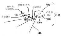
예컨대, 회전 다각형 스캐너의 동작을 설명해본다. 도 1은 대표적인 회전다각형 방식의 빔스캐닝시스템(101)의 주요특징을 예시하는 도면이다. 애플리케이션의 조건에 정합된 파장을 갖는 레이저 다이오드(102)는 필요하면 영상데이터 신호로 변조될 수도 있다. 빔 형성 광소자(104)는 원하는 형상과 궤적을 갖는 레이저 빔을 생성한다. 레이저 빔은 회전 다각형 미러(106), 특히 미러의 반사면들(108: facets)에서 반사되는데, 각 반사면들(108a)(108b)이 구별되도록 표시되어 있다. 회전 다각형(106)의 반사면들(108a)(108b)이 회전의 중심을 향하도록 배치되어 있어 미러 반사면이 회전하면서 입사빔이 각 미러 반사면을 쓸고지나가도록 빔 스캐닝 시스템(101)이 설계되어 있다. 이 빔은 일정한 편각만큼 꺽이어 주사된(선택적으로는 변조된) 빔(110)을 형성한다.For example, the operation of the rotating polygon scanner will be described. 1 is a diagram illustrating the main features of a representative rotating polygonal
회전 다각형방식 빔 스캐닝 시스템이 갖는 문제 중 하나는 회전 다각형 자체에 관한 것이다. 회전 다각형 미러는 비교적 큰 부피, 느린 속도증가, 대형, 소음, 베어링 신뢰성 문제, 비교적 큰 전력소모, 기타 단점들이 드러날 수 있다.One problem with rotating polygonal beam scanning systems relates to the rotating polygon itself. Rotating polygon mirrors can reveal relatively large volumes, slow speed increases, large size, noise, bearing reliability issues, relatively high power consumption, and other drawbacks.
전술한 바와 같이, 고속 바코드 스캐너는 소매점 계산대에서의 점포내 스캐닝과 고속 포장 선별과 같은 작업처리량 감응식 애플리케이션에 충분한 주사속도와 해상도를 제공하도록 회전 다각형 미러를 사용하는 것이 보통이다. 그러한 스캐너의 일예가 본 명세서에 원용된 Paul O. Detwilen의 미국특허 제 6,045,046 호, "FULL COVERAGE BARCODE SCANNER" 에 설명되어 있다. 다른 실시예들은 평행 주사 경로를 만들도록 다각형 반사면의 각도를 변경시키지 않는 대신에, 두번째 축선을 중심으로 진동하는 수직 스캔 미러를 주사경로에 구비하고 있다.As noted above, high speed barcode scanners typically use rotating polygon mirrors to provide sufficient scanning speed and resolution for throughput sensitive applications such as in-store scanning and high-speed packaging sorting at retail checkout counters. One example of such a scanner is described in US Pat. No. 6,045,046, "FULL COVERAGE BARCODE SCANNER," by Paul O. Detwilen, which is incorporated herein. Other embodiments have a scanning path with a vertical scan mirror that oscillates about the second axis instead of changing the angle of the polygonal reflecting surface to create a parallel scanning path.
전술한 대로, 주사빔 디스플레이는 빔 스캐너를 사용하기로 한다. 다양한 주사빔 디스플레이 장치들이 종래기술에 기술되어 있다. 그러한 실시예 중 하나는 여기서 원용되는 Furness 외의 미국특허 제 5,467,104 호, "VIRTUAL RETINAL DISPLAY" 에 설명된 바와 같은 주사빔 디스플레이를 포함한다. 마찬가지로, 전자사진식 프린터 (보통 "레이저 프린터"라 부른다), LIDAR 시스템, 회전 레이저 레벨, 문서 스캐너, 기타 빔 주사 시스템은 지금까지 회전 다각형 빔 스캐너들을 이용해왔다. 이러한 애플리케이션들은 회전 다각형 스캐너들을 이용하는 경우 고질적인 결함들을 가지고 있었다.As described above, the scanning beam display uses a beam scanner. Various scan beam display devices are described in the prior art. One such embodiment includes a scanning beam display as described in US Pat. No. 5,467,104, "VIRTUAL RETINAL DISPLAY", et al., Incorporated herein by reference. Similarly, electrophotographic printers (commonly referred to as "laser printers"), LIDAR systems, rotary laser levels, document scanners, and other beam scanning systems have used rotating polygon beam scanners to date. These applications had inherent defects when using rotating polygon scanners.
다른 애플리케이션들에서는 빔 스캐너 성능은 주사주파수의 함수로서 주사각 × 미러 사이즈의 곱으로 특정하는 것이 편리하다. 통상적인 방식에 따라 이 곱은 "쎄타 D"(ΘD)라 하며, 여기서 쎄타는 기계적 주사각의 절반을 말하며 "D"는 미러사이즈를 말한다. 이 전문용어에 함축된 가정은 스캔 미러 표면의 정적 및 동적 변형은 허용 한계치, 흔히 편향된 광의 최단 파장의 1/5 (λ/5) 범위안에 유지된다는 것이다. 미러사이즈가 클 수록 빔 스폿의 회절한도가 더 작아지고, 편향각이 클 수록 스폿 열을 정렬시키는 일정 거리에 필드폭이 더 커지며, ΘD는 스캔라인에서 해상되는(즉, 표시되거나 검출되는) 스폿 갯수에 비례한다. 물론 주파수는 단위시간당 생성될 수 있는 스캔 라인 수에 관련된다. 그러므로, ΘD가 큰 스캐너 일수록 성능이 더 좋다.In other applications it is convenient to specify the beam scanner performance as a product of scan angle x mirror size as a function of scan frequency. In the usual way, this product is called "theta D" (ΘD), where theta refers to half the mechanical scan angle and "D" refers to the mirror size. The assumption implied in this terminology is that the static and dynamic deformations of the scan mirror surface remain within acceptable limits, often 1/5 (λ / 5) of the shortest wavelength of the deflected light. The larger the mirror size, the smaller the diffraction limit of the beam spot, and the larger the deflection angle, the larger the field width at a given distance to align the spot columns, and ΘD is the spot resolved (ie, displayed or detected) in the scanline. It is proportional to the number. The frequency is of course related to the number of scan lines that can be generated per unit time. Therefore, the larger the scanner, the better the performance.
종래 기술에 의하면, 충분한 미러 평탄성을 유지하면서 높은 스캔 주파수로 높은 ΘD를 얻기란 비교적 어렵다고 알려져있다. 미러들이 비교적 큰 스캔각도, 높은 주파수 그리고 큰 미러사이즈의 조합으로 동작될 때 미러를 평탄하게 유지함에 있어서 스캔 미러에 가해지는 동적 응력은 장애가 된다.According to the prior art, it is known that it is relatively difficult to obtain high Θ D at a high scan frequency while maintaining sufficient mirror flatness. When the mirrors are operated at a combination of relatively large scan angles, high frequencies and large mirror sizes, the dynamic stresses applied to the scan mirrors are a barrier in keeping the mirrors flat.
본 발명의 한 양태에 의하면, 미소전자 기계적 시스템(MEMS) 빔 스캐너는 고성능을 달성한 것으로 설명되어 있다. 특히, 다양한 실시예들은 비교적 높은 스캔 주파수에서 비교적 큰 ΘD 곱을 갖도록 실시될 수 있다.According to one aspect of the present invention, microelectromechanical system (MEMS) beam scanners have been described as achieving high performance. In particular, various embodiments may be implemented to have a relatively large ΘD product at relatively high scan frequencies.
다른 양태에 의하면, 지금까지 회전 다각형 스캐너의 영역에 있었던 애플리케이션들에 사용할 수도 있는 성능과 특성들을 갖는 MEMS 빔 스캐너가 제공된다. 이러한 접근방법을 사용함으로써 부피와 질량이 줄고, 시동이 빨라지며, 소음이 줄고 안정성이 높아지는 등 회전 다각형 미러에 비해 다른 장점들이 가능해진다.According to another aspect, a MEMS beam scanner is provided having performance and characteristics that may be used for applications that have been in the area of rotating polygon scanners so far. This approach offers other advantages over rotating polygon mirrors, such as reduced volume and mass, faster start-up, less noise and increased stability.
이 발명의 한 양태에 의하면, MEMS 빔 스캐너는 미러 사이즈, 스캔 각, 스캔 주파수 및 미러 평탄성을 포함한 물리적 및 조작상의 속성들을 갖도록 형성하여 일정 범위의 애플리케이션들에서 회전 다각형 미러를 대체하도록 특별히 설계될 수도 있다. 어떤 애플리케이션들의 경우, 주사 축선을 가로질러 확장된 길이를 갖는 MEMS미러가 기존 광학 디자인에 대한 실질적인 변형을 하지 않고서 회전 다각형을 대신할 수 있다.According to one aspect of this invention, a MEMS beam scanner may be specifically designed to have physical and operational attributes including mirror size, scan angle, scan frequency and mirror flatness to replace a rotating polygon mirror in a range of applications. have. In some applications, MEMS mirrors with an extended length across the scanning axis can replace the rotating polygon without making substantial modifications to existing optical designs.
다른 양태에 따르면, MEMS 스캐너는 큰 스캔각에 적합한 토션 암 형상을 갖도록 형성된다. 이 토션 암(torsion arm)은 미러 표면의 길이방향 치수보다 몇 배 더 클수도 있다.According to another aspect, the MEMS scanner is formed to have a torsion arm shape suitable for large scan angles. This torsion arm may be several times larger than the longitudinal dimension of the mirror surface.
다른 양태에 따르면, (스캔 미러에서 떨어진 쪽으로) 토션 암의 말단부에는 지렛대 부재(leverage member)가 형성된다. 이 지렛대 부재는 응력 집중을 감소시키는 기능을 하면서 스캔각을 확대시키고, 측방이동된 장착패드에 접속부를 제공하고, 오프칩(off-chip) 액추에이터에서 스캐너를 구동시키는 모멘트암을 생성시킨다.According to another aspect, a lever member is formed at the distal end of the torsion arm (away from the scan mirror). This lever member serves to reduce stress concentration, expanding the scan angle, providing a connection to the laterally shifted mounting pad, and creating a moment arm for driving the scanner in an off-chip actuator.
이 발명의 다른 양태에 따르면, MEMS 스캐너는 클램핑 압력을 사용하여 액추에이터 조립체에 장착되고, 이 클램핑 압력은 선형 액추에이터와 실질적으로 연속 접촉하도록 마운팅 패드들을 잡아준다. 예컨대, 선형 액추에이터가 압전 액추에이터 스택(piezo-electric actuator stack)인 경우 이런 양압이 압전 액추에이터 스택에 압축력을 유지시키거나 인장력을 최소화 시킴으로써 안전성, 튼튼함 및/또는 수명을 개선한다.According to another aspect of this invention, a MEMS scanner is mounted to the actuator assembly using clamping pressure, which clamps the mounting pads into substantially continuous contact with the linear actuator. For example, if the linear actuator is a piezo-electric actuator stack, this positive pressure improves safety, robustness and / or life by maintaining compression force or minimizing tensile force on the piezoelectric actuator stack.
다른 양태에 의하면, 히터가 MEMS 토션 암의 스프링상수를 변화시키고, 그래서 토션 암에 지지된 스캐닝 미러의 공진 주파수를 변하게 한다. 이렇게 공진주파수 제어의 적합성이 얻어지면 MEMS 스캐너의 동작이 그 공진 주파수에 가까워진다. MEMS 스캐너 자체의 적어도 일부분에서 실리콘과 같은 벌크 반도체 물질을 주울 가열시킴으로써 가열이 이루어질 수 있다. 선택적으로 도핑공정이 완만한(graded) 저항대 길이를 갖는 전하 캐리어 채널을 생성한다. MEMS 스캐너의 영역들에 금속층들이 도표되어 그러한 영역들 내에 하위 주울 가열을 저감시킨다.According to another aspect, the heater changes the spring constant of the MEMS torsion arm and thus the resonant frequency of the scanning mirror supported on the torsion arm. When the suitability of the resonance frequency control is thus obtained, the operation of the MEMS scanner approaches the resonance frequency. Heating may be accomplished by Joule heating a bulk semiconductor material such as silicon in at least a portion of the MEMS scanner itself. Optionally, the doping process creates a charge carrier channel with a graded resistance band length. Metal layers are plotted in the areas of the MEMS scanner to reduce the lower joule heating in those areas.
다른 양태에 의하면, MEMS 스캐너는 사진석판식으로 형성된 프레임과 같은 외측 프레임을 갖지 않도록 형성될 수 있다. 대신에 다수의 마운팅 패드들이 형성될 수 있다.According to another aspect, the MEMS scanner may be formed so as not to have an outer frame such as a photolithographic frame. Instead, multiple mounting pads can be formed.
다른 양태에 의하면, 다수의 마운팅 패드들을 갖는 실리콘 웨이퍼 위에 다수의 MEMS 스캐너들이 형성될 수 있다. 지금까지는 프레임이 차지하였을 인접한 다이들 지역안으로 마운팅 패드들이 겹치도록 밀고 들어오는 엇매김 방식으로 실리콘 웨이퍼 위에 불규칙한 형상의 소자들이 형성된다. 딥 리액티브 이온에치(DRIE) 다 같은 딥에칭 프로세스를 이용하여 실리콘 웨이퍼에서 소자들이 거의 제거된다. 하나 이상의 "팬드" 또는 "브리지"들이 파트와 웨이퍼 사이 또는 인접한 파트들 사이에 접속을 유지하여 웨이퍼를 기계적으로 안정화시킨다. 이어서 브리지들을 파쇄하여 파트들을 제거시킨다.In another aspect, multiple MEMS scanners can be formed on a silicon wafer having multiple mounting pads. Until now, irregularly shaped devices are formed on a silicon wafer in a staggered manner where the mounting pads push in overlapping regions into adjacent dies that would have occupied the frame. Devices are almost removed from the silicon wafer using a deep etch process such as deep reactive ion etch (DRIE). One or more "pandas" or "bridges" maintain a connection between the part and the wafer or between adjacent parts to mechanically stabilize the wafer. The bridges are then broken to remove the parts.
다른 양태에 의하면, 스캐너 컨트롤러는 시스템 동작 주파수와 일치하는 스캐너 공진주파수를 유지하는 설비를 포함한다. 예시된 실시예에서 이는 위상차 피동 서보제어 루프로 실현된다.In another aspect, the scanner controller includes a facility for maintaining a scanner resonant frequency that matches the system operating frequency. In the illustrated embodiment this is realized with a phase difference driven servo control loop.
다른 양태에 의하면, 스캐너 컨트롤러는 스캐너 히터에 전류를 인가하기 위한 히터 증폭기를 포함한다.According to another aspect, the scanner controller includes a heater amplifier for applying a current to the scanner heater.
다른 양태에 의하면, MEMS 스캐너 컨트롤러는 스캐너 위상을 시스템 위상에 고정시키기 위한 위상 서보제어 루프를 포함한다.According to another aspect, the MEMS scanner controller includes a phase servo control loop to lock the scanner phase to the system phase.
다른 양태에 의하면, 스캐너 컨트롤러는 시스템 아이들 프로세스 중에 가상잠금상태(pseudo-locked state)로 동작하는 하나이상의 서보루프들을 포함한다.According to another aspect, the scanner controller includes one or more servo loops operating in a pseudo-locked state during a system idle process.
다른 양태에 의하면, MEMS 스캐너 컨트롤러는 작동중에 사용된 구동전압보다 상당히 더 높은 구동전압을 시동중에 인가한다. 높은 구동전압이 더 빠른 시동을 달성하는데 유용하다.According to another aspect, the MEMS scanner controller applies at start up a drive voltage significantly higher than the drive voltage used during operation. High drive voltages are useful for achieving faster startup.
도면의 간단한 설명Brief description of the drawings
도 1은 회전 다각형 스캐너가 달린 빔 스캐닝 시스템을 예시하는 도면1 illustrates a beam scanning system with a rotating polygon scanner.
도 2A는 일 실시예에 따라 만들어진 MEMS 스캐너의 평면도2A is a top view of a MEMS scanner made in accordance with one embodiment
도 2B는 다른 실시예에 따라 만들어진 MEMS 스캐너의 평면도2B is a top view of a MEMS scanner made in accordance with another embodiment
도 은 다른 실시예에 따라 만들어진 MEMS 스캐너의 사시도Is a perspective view of a MEMS scanner made in accordance with another embodiment;
도 4는 도 3의 MEMS 스캐너의 동적 응답을 보여주는 그래프4 is a graph showing the dynamic response of the MEMS scanner of FIG.
도 5A는 제작중에 실리콘 웨이퍼 위에 배열되는 방식을 보여주는 다수의 MEMS 소자들의 도면5A is an illustration of a number of MEMS devices showing how they are arranged on a silicon wafer during fabrication.
도 5B는 웨이퍼상에 MEMS 소자들의 다른 배치를 보여주는 도면5B shows another arrangement of MEMS devices on a wafer.
도 6은 MEMS 장착 클램프의 도면6 is a view of the MEMS mounting clamp.
도 7은 도 6의 액추에이터를 형성하는데 사용된 압전스택의 상세도7 is a detail view of the piezoelectric stack used to form the actuator of FIG.
도 8은 빔 스캐닝 서브시스템에 사용할 MEMS 스캐너 패키지의 정면 사시도8 is a front perspective view of a MEMS scanner package for use with the beam scanning subsystem
도 9는 도 8의 MEMS 스캐너 패키지의 두 추가 사시도9 is a further perspective view of the MEMS scanner package of FIG.
도 10은 MEMS 스캐너를 구동시키는 제어시스템의 블록도10 is a block diagram of a control system for driving a MEMS scanner.
도 11은 MEMS 스캐너를 구동시키는 시동방법을 보여주는 흐름도이다.11 is a flowchart showing a startup method for driving a MEMS scanner.
이하, 첨부한 도면과 상세한 설명, 청구항 들을 참조하면서 이 발명을 더욱 상세히 설명한다.Hereinafter, the present invention will be described in more detail with reference to the accompanying drawings, detailed description, and claims.
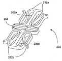
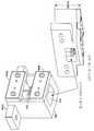
도 2A는 고성능 MEMS 스캐너(202)의 한 실시예를 도시한다. MEMS 스캐너(202)는 예컨대 고속, 고해상 LBP, 고속 바코드 스캐너, 주사 빔 디스플레이, LIDAR 시스템, 스캐너 레이저 레벨 등의 애플리케이션을 포함하여 다양한 애플리케이션들에 사용될 수 있다. MEMS 스캐너(202)는 종래기술로 알려져있는 벌크 미소기계가공(bulk micromachining)을 사용하여 단결정 실리콘으로 사진 석탄식으로 형성된다. 미러 표면을 지닌 스캔 플레이트(204)는 각자의 현가장치(suspensions)를 통해 1쌍의 토션 암(206a)(206b)에 결합되고, 이 현가장치는 현가 빔(208a),(208b),현가 중심 커넥터(218a)(218b), 및 현가 외측 커넥터(216a)(216b)(216c)(216d)로 구성된다. 토션 암(206a)(206b)은 스캔 플레이트(204)와 현가 빔(208a)(208b)이 돌아가는 회전축선(210)을 형성한다. 이 출원과 함께 양도되고 이 출원에 원용되며 2004년 5월 14일자 Randall B. Sprague 외가 발명출원한 미국 예비특허출원 제 60/571,133 호 「MEMS DEVICE HAVING SIMPLIFIED DRIVE」에 설명한 대로, 스캔 플레이트(204)의 표면에 걸쳐 토션 암(206a)(206b)에 의해 유도된 토크 부하를 분산시킴으로써 현가장치는 미러표면을 ¼파장 범위내에서 비교적 편평하게 유지시키는데 도움을 준다.2A illustrates one embodiment of a high
현가 빔들(208)은 각자의 외측(측방) 커넥터들(216a,216b,216c,216d)와 각자의 축방향 커넥터 (218a,218b)에 의해 스캔 플레이트(204)에 각각 결합된다. 모아 놓으면 현가장치 요소들(208a,216a,216b 및 218a)은 제 1 토션 암(206a)와 스캔 플 레이트(204) 사이에 제 1 현가 커플링을 형성한다. 마찬가지로 현가장치 요소들(208b,216c,216d 및 218b)는 제2 토션 암(206b)와 스캔플레이트(204) 사이에 제 2현가 커플링을 형성한다.Suspension beams 208 are coupled to scan
토션 암(206a,206b)는 각자의 "지렛대 부재"(212a,212b)로 마감된다. 지렛대 부재(212a)(212b)는 표시된 바와 같이 각자의 측방 지점들에서 각자의 마운팅 패드를(214a,214b)(214c,214d)에 연결된다. 전체적으로 보면, 지렛대 부재(212a)와 마운팅 패드를(214a,214b)는 토션 암(206a)을 지지구조물(도시안됨)에 결합시키는 제 1 마운팅 구조물을 구성한다. 마찬가지로, 지렛대 부재(212b)와 마운팅 패드들(214c,214d)는 토션 암(206b)을 지지구조물(도시안됨)에 결합시키는 제 2 마운팅 구조물을 구성한다. 대안의 실시예에서, 마운팅 구조물들은 각자의 토션 암에 직접 연결된 1쌍의 장방형 장착패드들, 스캔 플레이트(204)와 토션 암들(206a,206b)의 주변에 형성된 단일 프레임등의 다른 형태를 취할 수 있다. 도 2A의 실시예는 예컨대 웨이퍼당 더 많은 소자들을 채우거나, 동적응력을 저감시키거나, 개별 장착 패드들이 액추에이터에 결합되도록 하거나, 장착 패드들(214)이 서포에 대해 "떠있게"(float)하여 MEMS 스캐너의 잔류 응력을 저감시키는 등의 잇점을 갖게할 수 있다.The
대안의 실시예에서, 지렛대 부재들(212a,212b)이 측방지점들에서 주변의 장착프레임에 연결되고, 이 주변 프레임은 통상의 MEMS 배열에 따라 스캔 플레이트, 토션 암, 및 지렛대 부재들을 둘러싸고 있다.In an alternative embodiment, the
스캔 플레이트(204)와 그 위의 미러는(회전축선(210)에 평행한 방향의) 종방 향 길이보다 실질적으로 더 큰 (회전축선(210)에 수직한 방향의) 측방향 길이를 갖도록 구성될 수도 있다. 기타 고려사항들 중에, 이것은 회전 다각형 미러의 반사면을 흉내내도록 하는데 유리하게 사용되어, 다양한 애플리케이션들에서 스캐너(202)가 회전 다각형 스캐너 대신에 사용 될 수 있게 한다. 이와 달리, 스캔 플레이트(204)는 주어진 애플리케이션에 적합하게 더 낮은 종횡비의 장방형, 정사각형, 원형, 다원형 등으로 구성될 수 있다.The
도 2A에 표시한 대로, MEMS 스캐너(202)는 2개의 토션 암들(206a),(206b)을 포함하며, 각 토션 암은 필릿(fillet)을 포함해서 길이가 18.76mm이고, 기단부의 현가장치, 특별히 현가 빔들(208a,208b)은 400 미크론 × 200 미크론의 타원형 필릿으로 마무리 되고, 말단부의 지렛대 부재(212a,212b)는 400 미크론 × 200 미크론 타원형 필릿으로 마무리된다. 토션 암(206a,206b)의 폭은 384 미크론이다. MEMS 스캐너(202)의 나머지와 마찬가지로 토션 암들은 DRIE 프로세싱을 사용하여 전체 웨이퍼 두께 700 미크론까지 부식된다. 주어진 미러 질량에 대하여 토션 암과 지렛대 부재의 폭, 깊이 및 길이는 선택적인 공진 스캔 주파수와 각도를 생성하도록 조정될 수 잇다.As shown in FIG. 2A,
현가 빔들(208a)(208b)은 폭이 396 미크론이고, 약간 구부러져 있어 각자의 토션 암들(206a)(206b)와 91.6°의 약간 둔각을 이루며 스캔 플레이트(204)의 측방길이와 같은 정도로 측방으로 연장된다. 각자의 현가 중심 커넥터(218a)(218b)는 현가 빔(208a)(208b)의 중심선에서 스캔플레이트(204)의 중심선까지 (필릿을 포함해서) 500 미크론 정도 연장한다. 중심 커넥터(218a)(218b)는 각각 폭이 164 미크 론이고, 양끝에 100 미크론 반경의 필릿을 포함한다. 4개의 현가외측 커넥터(216a),(216b),(216c) 및 (216d)가 현가 빔(208a)(208b)의 끝에서 스캔 플레이트(204)까지 뻗어있고 도시한 대로 각 현가 빔의 끝에 하나씩 있다. 외측 커넥터(216a)(216b)(216c)(216d)는 각각 250 미크론 폭(측방향) X 400 미크론 길이(종방향)이고 필릿을 갖지 않는다. 그래서 각자의 현가장치들은 현가 빔(208), 중심현가 커넥터(218), 및 2개의 외측 현가 커넥터들(216)를 포함하며, 응력집중을 저감시키고 토크 부하를 분산기키며 작동중에 스캔 플레이트의 동적 변형을 저감시키도록 토션 암들(206a,206b)을 스캔 플레이트(204)에 연결한다. 다른 방식의 현가장치 구성도 가능하며 당업자들이 구현시킬 수도 있다.
도 2A 실시예의 스캔 플레이트는 6mm × 6mm 정사각형이다. 지렛대부재(212a,212b)는 1.8mm길이 (필릿포함 총 측방향치수) × 400 미크론 폭(종방향치수)이고, 도 2A의 실시예에서는 토션 암(206a)(206b)에 의해 형성된 축선에 수직하게 대칭적으로 뻗어있다. 지렛대 부재(212a)(212b)의 외측 단부들은 도시된 바와 같이 반경 200 미크론 필릿으로 각자의 장착패드 (214a,214b,214c,214d)에 연결된다. 장착패드들은 각각 5mm 정사각형이다.The scan plate of the Figure 2A embodiment is a 6mm x 6mm square. The
장착패드를(214a),(214b),(214c) 및 (214d)위와 (220a)와 (220b)에는 도핑된 채널들이 형성된다. 도핑 채널들 밑에있는 장착 패드들(214a)(214b)(214c) 및 (214d)에 금속이 침착되어 있다. 스캔 플레이트(204) 위에도 금속이 침착되어 있어 중심 현가 커넥터들(218a)(218b)위를 지나 도핑된 채널들(220a)(220b)과 겹치는 지점까지 뻗어있다. 후술하는 바와 같이, 도핑 채널들은 비금속 영역과 금속층 사이 에 전류가 흐를 수 있게 비교적 낮은 등급의 저항을 갖는 영역들을 형성한다. 예컨대 금이나 알루미늄과 같은 금속으로 스캔 플레이트(204)위에 미러면을 형성한다.Doped channels are formed over the mounting
지렛대 부재의 형상이 바뀔 수 있다. 마찬가지로 장착 패드의 형상, 크기, 모양, 지렛대 부재와의 연결 방향등이 애플리케이션 조건에 따라 조정될 수 있다. 부가적으로 MEMS 스캐너(202)의 지렛대 부재, 장착 패드, 기타 부품들이 애플리케이션 조건들에 따라 비대칭적으로 성형될 수 있다. 예컨대. 도 2B와 연관하여 보이듯이 두 장착패드들, 두 지렛대 부재들, 그리고 하나의 토션 암으로 된 전체 조합이 제거될 수도 있다.The shape of the lever member may change. Similarly, the shape, size, shape of the mounting pad and the direction of connection with the lever member can be adjusted according to the application conditions. Additionally, the lever members, mounting pads, and other components of the
스캔 플레이트(204), 소자들(208a,216a,216b,218a)와 (208b,216c,216d,218d)에 각각 대응하는 현가 장치들의 형상이 마찬가지로 변경될 수 있다. 예컨대, 4mm × 4mm 스캔 플레이트(204)가 도 2A의 6mm × 6mm 스캔 플레이트로 대체되면 토션 암 길이가 각각 12mm 씩 단축될 수 있지만 거의 일정한 공진주파수와 소재응력한계를 유지한다. 스캔 플레이트 동적 변형을 저감하는 잇점을 유지하면서 현가 장치들도 변경될 수 있다.The shape of the suspension devices corresponding to the
장착 패드들(214a,214b,214c 및 214d) 또는 다른 주변 프레임이 하우징에 장착될 경우, 액추에이터(도시안됨)에 주기적으로 전원을 인가하면, 토션 암들(206a,206b)이 그리는 회전축선(210)을 중심으로 스캔 플레이트(204)가 주기적으로 정회전하고 역회전한다. 한 실시예에서 (4개 액추에이터 실시예의 경우 0과 25-30 사이에서 변하는 5㎑ 정편파와 같은) 적절한 신호로 구동될 때 스캔플레이트(204)는 5㎑ 주파수에서 ±20° 기계적 주사각으로 응답한다.When the mounting
±20°의 기계적 스캔각도에서 스캐너(202)는 9변 회전다각형과 거의 동등한 스캔각을 나타낸다. 다른 다각형상과 일치 하도록 다른 스캔각이 선정될 수 있다. 5㎑의 전주기 스캔 속도에서 스캐너(202)는 10㎑의 속도로 이방향 스캔 (각 사이클당 1회의 순방향 주사와 1회의 역방향 주사)를 생성한다. 이는 66,667 RPM으로 회전하는 9변 다각형 미러와 거의 등등하다. 그래서 스캐너(202)는 비교적 정교한 회전 다각형 스캐너의 스캐닝 성능을 달성하여 고속 애플리케이션에 적합하게 된다. 대안으로 스캐너는 일방향으로 주사하는데 사용될 수 있어 33,333RPM 9변 회전 다각형 스캐너와 거의 동등하게 된다. 미러가 순방향 또는 역방향 주사 반사이클 중 어느 하나일 때만 영상 데이터를 변조하거나 영상 데이터를 포획함으로써 일방향 조작이 간단히 이루어진다. 이방향으로 사용될 때 역방향 주사중에 데이터 판독을(레이저 방향으로 또는 검출기로 부터) 역전시키는데 적절한 제어전자 장치가 사용된다.At a mechanical scan angle of ± 20 °, the
도 2B는 MEMS 스캐너(202)의 대안적 실시예를 나타낸다. 도 2A와 관련하여 설명한대로, 단일 토션 암이 현가장치를 통해 스캔 플레이트(204)를 지지한다. 다양한 모드의 공진 주파수를 적절히 제어하거나, 후술하는 바와 같이 공진 주파수나 그 주변주파수로 스캔 플레이느를 구동시킴으로써 스캔 플레이트가 축선(210)을 중심으로 회전할 수 있다.2B illustrates an alternative embodiment of the
도 3은 MEMS 스캐너(202)의 또 다른 실시예를 나타낸다. 도 3의 실시예에서, 지렛대부재(212a)(212b)는 뱀처럼 구부러진 형상으로 만들어진다. 지렛대 부재의 밑단부들은 전술한 대로 보통 장착 패드들에 연결되거나 주변 프레임 부재에 연결 된다. 아시다시피 지렛대 부재의 형상도 실질적으로 변경될 수 있다.3 shows another embodiment of a
도 4는 주기적인 구동신호가 인가될 때 도 2A의 MEMS 스캐너의 동작응답을 예시하는 그래프이다. 곡선(402)는 주기적 구동주파수(406)의 함수로서 진폭응답(404)을 나타낸다. 곡선(408)호 동일한 구동 주파수 축선(406)에 대하여 그려진 스캐너 대 구동위상(410) 예시한다. 곡선(402)을 점검해보면 회전모드에서 MEMS 스캐너의 공진 주파수에 대응하는 약 5㎑에서 피크응답치를 나타낸다. 피크값의 크기는 상대적 기준을 두고 도시되어 있지만, 허용가능한 구동력에서 ±20°기계적 스캔각의 공진 응답을 생성하도록 도시된 실시예에서는 충분히 높게 되어있다. 액추에이터 실시예에서, 0(제로) 내지 25-30 볼트 진폭을 지닌 5㎑ 정현파에 근접한 구동 파형이 ±20° 기계적 주사각을 나타낸다.4 is a graph illustrating an operation response of the MEMS scanner of FIG. 2A when a periodic driving signal is applied.
65와 70 ㎑ 사이의 2차 피크값은 압전 스택 액추에이터의 공진 특성에 대응한다.The second peak value between 65 and 70 Hz corresponds to the resonance characteristic of the piezoelectric stack actuator.
곡선(408)은 MEMS 스캐너 응답에 대한 구동 신호의 위상관계가 공진지점에서 어떻게 반전하는지를 보여준다. 5㎑ 미만에서 위상관계(구동신호 대 응답)는 0°이다. 5㎑이상이지만 2차 피크값 미만에서 위상관계는 -180°이다. 1차 공진 피크값에서 위상관계는 반전되고, 도시한 대로 -90°(응답지연 구동)를 지나간다. 2차 피크값 이상에서 시스템의 응답은 떨어지고 위상응답은 다시 반전하여, 피크값 아래서 -180°를 지나, 2차 피크값에서 -270°(+90°), 2차 공진 피크값 이상의 주파수에서 -360°(0°)를 통과한다. 효과를 극대화시키기 위하여 1차 공진 피크값이나 바로 부근에서 MEMS 스캐너를 조작하는 것이 유리하다고 밝혀졌다.
5㎑ 운전에서 MEMS 스캐너의 공진 주파수는 5㎑ 이상의 수 ㎐, 보통 실온에서 5.001 내지 5.005 범위로 조정된다. 그러한 조정은 이 출원과 함께 양도되고 이 명세서에 원용되는 미국특허 제 6,245,590 호 "FREQUENCY TUNABLE RESONANT SCANNER AND METHOD OF MAKING"에 서술된 방법들을 사용하여 달성된다. 소량의 에폭시 형태로 스캔 플레이트에 하중을 더하는 방법을 사용하여 공진주파수를 공장조정(fuctory trim) 하는 것이 유리한 것으로 알려져 있다. 공진주파수의 활성 열튜닝(active thernal tunning)을 사용하여 공진주파수를 실질적으로 5.000㎑가 되게한다.In a 5 Hz operation, the resonant frequency of the MEMS scanner is adjusted to a range of 5.001 to 5.005 at several Hz, usually at room temperature. Such adjustment is accomplished using the methods described in US Pat. No. 6,245,590, "FREQUENCY TUNABLE RESONANT SCANNER AND METHOD OF MAKING," which is assigned with this application and incorporated herein. It is known to advantageously trim the resonant frequency using a method of adding a load to the scan plate in the form of a small amount of epoxy. Active thermal tuning of the resonant frequency is used to make the resonant frequency substantially 5.000 Hz.
도 5A는 100mm 실리콘 웨이퍼(502)위에 MEMS 스캐너들(202a,202b,202c,202d, 202e 및 202f)을 표준배치한 것을 나타낸다. 도시한 대로 MEMS 스캐너들은 손바닥 모양의 장착 패드들과 미러들로 빼곡이 채워져 있다. 그러한 배치를 한 이유는 웨이퍼당 산출량을 극대화하기 위함이다. 도 5A에 도시된 스캐너(202)의 스캔 플레이트는 짧고 넓은 종횡비로 형성되어 있다.5A shows a standard arrangement of
도 5B는 100㎜ 실리콘 웨이퍼에서 제작된 MEMS 스캐너의 다른 배치도를 나타낸다. 스캐너들의 치수, 특히 토션 암의 길이는 도 5A의 배치에 비하여 더 효율적인 손가락 모양의 패킹이 되도록 조정될 수 있다. 웨이퍼가 클수록 소자들이 더 고밀도로 패킹된다.5B shows another layout of a MEMS scanner fabricated on a 100 mm silicon wafer. The dimensions of the scanners, in particular the length of the torsion arm, can be adjusted to be more efficient finger-shaped packing compared to the arrangement of FIG. 5A. The larger the wafer, the denser the elements are packed.
여기서 " 손가락 모양(interdigitated)"이란 용어는 하나이상의 인접한 반도체 소자들의 일부를 절개하지 않고서 한 반도체소자 둘레에 정사각형을 그릴 수 없다는 것을 의미한다. 즉, 하나이상의 인접하는 반도체 소자들은 다이싱 돕(dicing saw)을 사용하여 그 반도체 소자 주위에 형성될 수 있는 형상의 윤곽안으로 침입한다. 심층 반응이온부식(DRIE)와 같은 에칭단계나 다른 프로세스 단계를 사용하여 웨이터로부터 스캐너들을 거의 완벽하게 떼어낼 수 있다. 각 소자 주위에 형성된 이중선은 이 소자 주위에 형성된 "해자(moat)"의 가장자리를 나타낸다. 매우 미세한 실리콘 "브리지들(bridges)"이 일전간격을 두고 스캐너들을 웨이퍼에 연결하는 것으로 보일 수 있다. 스캐너들을 떼어내기 위해 이 브리지들을 간단히 깨뜨려 스캐너들이 튀어나오게 한다. 소자를 가로질러 균열이 퍼지지 않도록 브리지의 폭이 좁게 설정되어 있다.The term "interdigitated " herein means that a square cannot be drawn around a semiconductor device without cutting off a portion of one or more adjacent semiconductor devices. That is, one or more adjacent semiconductor devices intrude into the contour of a shape that can be formed around the semiconductor device using a dicing saw. Etching steps, such as deep reactive ion corrosion (DRIE), or other process steps can be used to almost completely remove the scanner from the waiter. Double lines formed around each device represent the edges of the "moat" formed around this device. Very fine silicon "bridges" may appear to connect the scanners to the wafer at intervals. To break the scanners, simply break these bridges so that the scanners pop out. The width of the bridge is set narrow so that cracks do not spread across the device.
다른 실시예에서, DRIE 전에 실리콘 웨이퍼의 배면에 금속층이 입혀지거나 절연체 웨이퍼가 접착된다. DRIE는 실리콘 웨이퍼를 통과해 에칭하는데 쓰인다. 그러면 금속층이나 절연체가 스캐너들을 웨이퍼에 잡아둔다. 이 금속을 잘래내어 스캐너들을 제거할 수 있다. 그와 달리, 금속이나 절연체를 부식시켜 파트들을 제거할 수도 있다. 한 실시예에서 금속 안정화층으로 알루미늄이 사용된다. 그러한 안정화층이 사용될 경우 형상을 적소에 유지시키도록 실리콘 브리지들이 사용될 수도 있다. 그와 달리 실리콘 브리지들이 제거될 수도 있다.In another embodiment, a metal layer is applied to the backside of the silicon wafer or the insulator wafer is adhered to before the DRIE. DRIE is used to etch through silicon wafers. The metal layer or insulator then holds the scanners on the wafer. This metal can be cut off to remove the scanners. Alternatively, parts can be removed by corrosion of the metal or insulator. In one embodiment aluminum is used as the metal stabilization layer. Silicon bridges may be used to keep the shape in place when such a stabilization layer is used. Alternatively, silicon bridges may be removed.
도 5A는 다른 지렛대부재(212)를 예시하며, 여기서 "T"의 단부들은 미러를 향해 치우쳐있다.5A illustrates another
몇가지 실시예들에 의하면 MEMS 스캐너(202)의 제작에는 전술한 바와 같은 도핑채널이나 전하캐리어층의 형성이 포함될 수 있다. 1-10 오옴의 벌크저항을 가진 인도핑된 실리콘 웨이퍼들이 사용된다. 인도핑처리된 실리콘 웨이퍼들에는 최대 전류4㎃에서 30KeV로 가속화된 5×10¹⁵인 31원자/㎠의 조사량이 주입된다. 인 분량은 1000℃에서 45분간 구동된다. 최종 도핑채널은 약 0.5 미크론의 깊이까지 강하게 도핑되어 갱신된 채널을 형성하고, 여기서 도핑 농도와 최종 저항은 깊이에 따라 변화한다. 이런 조건하에서 웨이퍼 표면은 약 1×10²⁰ 인 31원자/㎤의 도핑농도를 갖고 약 0.001Ω-㎝의 저항을 나타내며, 이는 0.5 미크론의 깊이에서 약 1×10¹⁵ 원자/㎤(또는 1-10 Ω-㎝)의 웨이퍼 배경이 된다.According to some embodiments, fabrication of the
도핑 처리된 채널은 전하 캐리어가 금속층에서 실리콘 안으로 들어가는 도관을 만들어낸다. 후술하는 바와 같이, MEMS 스캐너(202)에 전류가 인가되어 주울 가열을 일으킨다. 도 2A 스캐너의 실시예에서, 예컨대 히터 증폭기에 의해 장착 패드들(214a, 214b)에 양전압이 걸릴 수 있다. 히터 리드선들이 장착 어셈블리에 결합되거나 장착 패드 자체위에 있는 금속화층에 결합될 수 있다. 예시된 실시예에서, 장착패드들(214a, 214b)을 덥는 금속층을 따라 전류가 흘러, 금속 밑에 형성된 도핑 채널을 거쳐 실리콘 안으로 이동한다. 그 다음에 전류가 실리콘 내부에서 지렛대 부재(212a)와 토션 암(206a)을 통해 흘러 주로 토션 암(206a)에 국부적 가열을 형성한다. 전류흐름이 지렛대 부재(212a)의 양쪽 팔들을 따라 분할되기 때문에 지렛대 부재안의 주울 가열이 저감된다. 토션 암(206a)이 도핑채널(220a)과 만나는 곳에서, 전류가 실리콘에서 흘러나와, 도핑채널(220a)에 겹쳐져 형성된 금속층 안으로 흘러 들어간다. 전류는 중심 현가 커넥터(218a)를 지나, 스캔 플레이트(204)에 형성된 미러의 금속을 지나, 그리고 중심 현가 커넥터(215b)를 지나서 이런 구 조물안의 주울 가열을 회피한다. 금속층이 도핑채널(220b)과 겹치는 곳에서, 전류가 금속에서 흘러내려 실리콘 안으로 흐른다. 전류가 토션 암(206b)과 지렛대부재(212b)를 통해 흘러, 다시 주로 토션 암 내부에서 주울 가열을 야기한다. 전류는 장착패드들(214c, 214d)에 형성된 토핑 채널을 통해 흘러 그 위에 형성된 금속층들 안으로 흐르며, 여기서 접지 근처에 고정된 제 2 조의 히터 리드들에 의해 수집된다. 종래기술에 알려진 대로 도시된 방향으로의 정공(hole) 이동이나 반대방향으로의 전자이동이 그러한 전류흐름을 형성할 수 있다.The doped channels create a conduit through which charge carriers enter the silicon in the metal layer. As will be described later, a current is applied to the
몇가지 경우에 있어서, 도 2A, 2B, 3, 5A 및 5B에 의해 도시된 스캐너 디자인의 유리한 측면은 최소한의 프로세스 단계들이 제작에 사용될 수 있다는 것이다. 일정영역의 두께를 낮추거나 높아진 리브들(raised ribs)을 생성하는 부분적인 에칭없이 실리콘 웨이퍼의 전두께에 걸쳐 스캐너들이 형성될 수 있다. 미러에 대응하는 금속화 패턴이 웨이퍼(502)의 정면에 형성된다. 한 실시예에 의하면 미러에 금 금속화가 사용된다. 웨이퍼(502)의 배면에는 배면 금속화가 성형된다. 한 실시예에 의하면, 배면 금속화층에 알루미늄이 사용된다. 다음에 반도체 소자들과 그 사이의 비에칭 영역들에 대응하는 포토레지스트 패턴이 웨이퍼의 정면에 형성되고, 노출된 영역은 딥에칭된다. 한 실시예에서, 웨이퍼를 통해 수직벽들을 에칭하는데 DRIE가 사용된다. 에칭도중에 웨이퍼의 배면이 저온냉각되고, 알루미늄 배면 금속화층의 높은 열전도성으로 인하여 DRIE 에칭이 실리콘 웨이퍼의 배면에 도달하면 정지된다. 어떤 실시예들에서, 에칭된 윤곽선들의 배면을 잇는 알루미늄층에 의해 웨이퍼에 스캐너 형상들이 유지된다. 다른 실시예들에서 실리콘의 얇은 브리지들이 파트 들을 적소에 보지하는데 도움을 준다. 알루미늄 배면 금속화층이 에칭되어 없어지고 포토레지스가 제거된다. 이때 스캐너들이 떨어져 나오거나, 실리콘 브리지들이 사용되는 경우 딥에칭 지역을 가로질러 브리지들을 끊어버림으로써 스캐너들이 웨이퍼에서 제거되어 단일화된다. 파트들을 분리시키는데 딥에칭을 사용함으로써 다이싱(dicing)을 피할 수 있다.In some cases, an advantageous aspect of the scanner design shown by FIGS. 2A, 2B, 3, 5A, and 5B is that minimal process steps can be used for fabrication. Scanners can be formed over the entire thickness of the silicon wafer without partial etching to reduce the thickness of the region or create raised ribs. A metallization pattern corresponding to the mirror is formed on the front of the
도 6은 MEMS 스캐너의 액추에이터 배열을 예시한다. 1쌍의 사용화된 압전 스택들(602a)와 (602b)는 공동 장착베이스(604)위에 얹혀 각자의 제 1 절연체들(606a)(606b)를 거쳐 MEMS 스캐너(202)의 장착 패드들(214a)(214b)을 지지한다. 각자의 위치들에서 압전 스택들(602a)(602b)은 전기적으로 압축과 팽창을 교대적으로 받으면서, 토션 암들(206a)(206b)이 정의하는 회전축선(210)을 중심으로 장착패드들(214a)(214b)의 주기적 회전을 일으킨다. 마찬가지로, 압전 스택(602a)(602b)의 공통모드 활성화를 이용하여, 스캔 플레이트(204)의 가로 축선에 실질적으로 평행하는 가로축선을 중심으로 MEMS 스캐너(202)를 회전시킨다.6 illustrates an actuator arrangement of a MEMS scanner. A pair of used
MEMS 스캐너(202)와 압전 액추에이터 스택들(602a, 602b)사이의 접촉을 유지시키기 위하여 각각의 클램프 또는 누름 어셈블리들(608a)(608b)(608b는 도시안됨)가 장착패드들(214a, 214b)을 액추에이터 스택들에 대고 누른다. 간단히 보이도록 도 6에서 클램프(608b)가 생략되어 있다. 도시한 대로 장착패드(214)와 접촉하여 있는 어셈블리의 바닥부터 시작해서 클램프들(608)은 제 1 누름판(610), 선택적인 시리즈 디스크 스프링(612), 제 2 누름판(614), 제 2 절연체(616), 그리고 제 3 누름판(618)을 포함한다. 한 실시예에서, 제 1 누름판(610)의 가장자리가 도시한 바 와 같이 누름 어셈블리에서 밖으로 뻗어나온다. 후술하는 바와 같이, 이것은 히터선이나 리드에 대한 선택적인 접착위치를 제공한다. 시리즈 디스크 스프링(612)는 SPRINGMASTERS#D 63203과 같은 상용타입이고, 강직성은 비교적 낮지만 고유공진주파수는 높은(775㎑)것이 되도록 선택된다. 애플리케이션 조건에 따라 직렬스프링 2개, 다른 개수의 스프링이 사용되거나 아예 스프링이 전혀 사용되지 않을 수도 있다. 제 1 및 제 2 누름판(610)과 (614)는 시리즈 디스크 스프링(612)이 눌러대는 튼튼한 표면을 제공한다. 제 2 절연체(616)는 MEMS 스캐너(202)의 전기적 절연을 제공한다. 제 1 및 제 2 절연체(606)(614)는 DYREX 유리와 같이 적절한 밀도, 전기절연성 및 압축강도를 갖는 소재로 형성된다. 제 1 및 제 2 누름판(610)(614)는 적절하게 전기전도성이 있고 강철과 같이 압축강도, 조도 및 밀도를 포함한 물리적 성질을 갖는 소재로 형성된다. 제 3 누름판(618)은 제 2 절연체(616)를 위한 장착표면을 제공하고, 어셈블리를 하우징(도시안됨)에 연결시킨다. 바람직하게는 강철로 형성된 제 3 누름판(618)은 장착 및 조정 나사(도시안됨)를 수용하는 보어(620)를 포함한다. 당업자라면 알 수 있듯이 대안의 변형된 클램프들이 사용될 수도 있다.Respective clamps or
대안의 실시예에서 시리즈 디스크 스프링(612)이 누름 어셈블리(608)에서 제외될 수 있다고 알려졌다. 그러한 변형이 조립의 용이성과 비용면에서 유리하지만 어느정도 구동효율을 손상시킬 수도 있을 것이다.In alternative embodiments it is known that the
누름 어셈블리(608)의 한두개 부품들이 선택적으로 하우징에 키 고정되거나, 그렇지 않으면 실질적으로 고정된 회전관계로 보지될 수 있다. 이렇게 되면 장착 및 조정나사의 조정중에 어셈블리를 통해 전달된 토크부하를 저감시키거나 제거할 수 있을 것이다. 누름 어셈블리들(608)을 통한 토그부하를 실질적으로 저감시키거나 제거함으로써, 조립중에 MEMS 스캐너의 장착패드들(214)에 인가되는 토크부하가 사실상 제로가 되어, 장착패드들(214)이 약간 회전하여 생기는 공진주파수 및/또는 주사각 범위의 불리한 변동이 생기지 않도록 MEMS 스캐너(202)를 보호한다.One or two parts of the pressing assembly 608 may optionally be keyed to the housing or otherwise held in a substantially fixed rotational relationship. This will reduce or eliminate the torque load transmitted through the assembly during mounting and adjustment screw adjustment. By substantially reducing or eliminating the torque load through the press assemblies 608, the torque load applied to the mounting pads 214 of the MEMS scanner during assembly is virtually zero, causing the mounting pads 214 to rotate slightly. The
도 7은 압전 스택 액추에이터(602)의 도면이다. 그러한 액추에이터는 http://www.physikinstrumente.de model PICMA 885.10을 포함한 몇개의 소스들로부터 구입할 수 있다.7 is a diagram of a
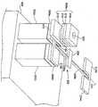
도 8과 도 9는 LBP, 바코드 스캐너, LIDAR, 스캔 레이저 레벨등에 사용할 MEMS 스캐너 하우징(802)의 도면들이다. 2개의 정면판(804a)(804b)가 장착 나사들(808a, 808b, 808c, 808d)에 의해 배면 하우징(806)에 조여진다. MEMS 스캐너(202)는 적절한 회전량만 허용되는 공동안에 보지된다. 나사홈이 있는 조정나사구멍(810a, 810b, 810c 및 810d)는 해당 조정나사 수용공(620)(도 6에 도시됨)안으로 돌출하는 조정나사(도시안됨)를 수용한다. 조립중에 조정나사를 돌려 시리즈 디스크 스프링(612)(도시안됨)에 적절한 양의 예비부하를 제공한다. 배면 하우징(806)의 맨위에 형성된 MEMS 관찰구(812)를 통해 작동중인 MEMS 스캐너의 거동을 관찰할 수 있다. MEMS 스캐너 에셈블리(802)는 하우징(806)에 형성된 장착탭(814a, 814b)를 거쳐 LBP의 노출장치에 고정된다.8 and 9 are diagrams of a
하우징(802)에 MEMS 스캐너(202)를 고정시키는데 클램프(608)를 사용하는 것은 "부동하는(float)"는 마운트가 되어 장착패드들(214)이 서로 약간씩 이동하게끔 한다. 몇 실시예들에서 조립중에 클램프들(608)을 약간 비틀면 장착패드들(214)이 동일 평면내에서 약간 비틀리게 된다. 이로써 MEMS 스캐너의 지렛대 부재 및/또는 토션 암들에 원치않는 잔류응력이 생길 수 있다. 저감된 스캔각도로 수시간동안 고정된 스캐너를 가동시키거나 "소진"(burning-in)시킴으로써 이러한 비틀림(twisting)이 제거되거나 저감될 수 있다. 예시된 실시예에서 스캐너는 거의 4시간 동안 절반의 진폭으로 가동된다. 이러한 소진 과정은 지렛대 부재들 및/또는 토션 암들의 기계적 고장과 관련된 "유치한" 고장의 발생율을 저감시킬 수 있다. 대안으로써 스캐너 어셈블리 소진의 필요성을 없애거나 줄이기 위해서 비틀림 감소 클램프 어셈블리 디자인으로 대체될 수도 있다.Using the clamp 608 to secure the
MEMS 스캐너(202)가 4개의 압전스택들(602)로 구동될 수 있고, 각 스택은 마운팅패드(214a)(214b)(214c) 및 (214d) 밑에 하나씩 설치된다. 대안으로 MEMS 스캐너의 일단부는 고정위치에 보지될 수 있다. 즉 마운팅 패드들(214c)(214d)이 견고한 마운팅 지점에 체결되고, MEMS 스캐너의 타단부는 압전 액추에이터들에 의해 구동될 수 있다. 즉 마운팅 패드들(214a)(214b)가 도 6에 도시된 대로 압전스택들에 체결될 수 있다. 세번째 대안으로서, 세개의 마운팅 패드들이 고정된 견고한 마운팅 지점에 체결되고 하나의 압전 스택 액추에이터가 사용된다. 전형적으로 비용대 액추에이터 전력 조건에 따라 선택이 갈린다. 아시다시피 도 2B 또는 도 3에 제시된 바와 같은 MEMS 스캐너(202) 디자인에 유사한 고려를 할 수도 있다.The
전술한 대로, 원하는 동작 주파수의 수 ㎐ 범위내에서 공진주파수를 갖도록 MEMS 스캐너가 조정된다. 도 4의 곡선(402)에서 알 수 있듯이, 공진주파수의 변화 가 조금만 있어도, 주어진 주기적 작동전압에 대해 회전진폭에 상당한 변동이 있게된다. 발명자들이 발견한 바에 의하면, 예시된 실시예에서 MEMS 스캐너가 외측 프레임을 갖지 않더라도 MEMS 장치의 가열을 제어하면 공진주파수와 작동진폭이 조정되었다. 다시 도 6을 참조하면, 클램프(608a)의 제 1 누름판(610)위에 뻗어있는 태브(tab)는, (도시안됨) 클램프(608b)의 해당 누름판이 그러하듯이, 히터 와이어를 수용한다. 마찬가지로, 마운팅 패드들(214c)(214d)(역시 도시되어 있지 않음)에 인접해 있는 해당 누름판들도 히터 와이어들을 수용한다. 이 히터 와이어들은 제 1 누름판의 튀어나온 금박 태브에 납땜하거나, 예컨대 마운팅 패드(214)위에 형성된 금속화 시리콘본드 패드에 납땜하거나, 당업자들에게 알려진 다른 방법들에 의해 부착될 수 있다.As described above, the MEMS scanner is adjusted to have a resonant frequency within the range of the desired frequency of operation. As can be seen from the
MEMS 스캐너의 일단부에 있는 두 마운팅 패드들 또는 클램프들에 히터 리드선들이 부착될 경우 인접한 리드선들 사이에 전류가 흐르지 않도록 리드선들의 전위가 동일하게 유지되는 것이 바람직하다. 반대로, MEMS 스캐너의 타단부에 있는 히터 리드선이나 리드선들은 토션 암들을 따라 전류흐름을 일으키도록 다른 전압으로 구동될 수도 있다.When heater leads are attached to two mounting pads or clamps at one end of the MEMS scanner, the potential of the leads is preferably kept the same so that no current flows between adjacent leads. Conversely, heater leads or leads at the other end of the MEMS scanner may be driven at different voltages to cause current flow along the torsion arms.
사용시에, 센서들이 스캔 크기를 감시하고, 스캐너(202)의 두 단부들(마운팅 패드(214a)(214b)가 일단부을 형성하고 마운팅 패드(214c)(214d)가 타단부를 형성한다)사이의 전위가 조정된다. 전류가 흐르도록 전술한 실리콘 소재 자체와 도핑채널, 특히 토션 암들(206a)(206b)의 저항에 의해 가열된다. 온도가 높을수록 토션 암들의 "연화"(softening)와 공진주파수의 대응하는 감소가 일어난다. 그래서 공진 주파수가 주기적인 구동신호 주파수 위에 있을 경우 가열이 증가되어 MEMS 스캐너의 온도가 증가되고, 그래서 이 구동신호 주파수에 일치하도록 공진주파수를 조정한다. 마찬가지로, MEMS 스캐너의 공진주파수가 구동신호 주파수 아래로 떨어질 경우 가열이 감소되어 장치를 냉각시키며 공진주파수를 구동신호 주파수에 일치하게 상승시킨다. 다른 실시예에서, 주어진 시스템 디자인에 대해 스캐너가 공진주파수에서 정확하게 작동하지 않는 경우라도 스캐크기를 변화시키기 위해 열 조정(thermal trimming)이 사용될 수 있다.In use, the sensors monitor the scan size and between the two ends of the scanner 202 (mounting
실험에 의하면 0∼1.5W의 튜닝전력이 약 8㎐의 공진주파수 튜닝범위을 제공한다고 알려졌다. 아마도 동작중에 스캐너 위로 흐르는 공기흐름이 냉각효과를 주는 결과, 위와 같은 범위는 스캐닝 주파수가 높을 수록 약간 더 낮고, 스캐닝 주파수가 더 낮을 수록 약간 더 높다.Experiments have shown that a tuning power of 0 to 1.5 W provides a resonant frequency tuning range of about 8 Hz. Perhaps the flow of air over the scanner during operation has a cooling effect, resulting in a slightly lower range at higher scanning frequencies and slightly higher at lower scanning frequencies.
도 10으로 다시 돌아가면, MEMS 스캐너를 구동시키기 위한 제어시스템(1002)를 보여주는 블록 다이어그램이다. 많은 애플리케이션들에 있어서 MEMS 스캐너의 위상과 진폭을 정학하게 제어하는 것이 유리하다. 바코드 스캐너, 레이저 카메라, 주사빔 디스플레이, 전자사진식 프린터 등을 포함하는 주사빔 애플리케이션들은 MEMS 스캐너 위상 및/또는 진폭의 정밀한 제어를 통해 이득을 볼 수 있다.Returning to FIG. 10 again, a block diagram shows a
마찬가지로, 스캐너 공진주파수의 정밀한 제어를 통해 전력소모를 최소화시킬 수 있고, 지금까지 흔히 시행되어오던 다소간의 공진 이탈이 아니라 스캐너의 동작을 바로 공진주파수에서 가능하게 함으로써 어떤 애플리케이션들이 가능하게 되었다.Similarly, precise control of the scanner's resonant frequency minimizes power consumption, and some applications have been made possible by enabling the scanner's operation directly at the resonant frequency, rather than the more or less resonant deviations commonly practiced up to now.
도 10의 제어시스템(1002)의 블록도는 MEMS 스캐너를 구동시키고 제어하는 3개의 중첩되는 서보루프들을 포함하는데, 즉 진폭제어 서보루프(1004), 위상제어 서보루프(1006), 그리고 주파수제어 서보루프(1008)이 각각 중간 쇄선, 짧은 쇄선, 긴 쇄선으로 표시되어 있다.The block diagram of the
우선 진폭제어 서보루프(1004)를 보면, 저전압 구동신호(1009)가 고전압 증폭기(1010)에 의해 증폭되어, 압전 드라이버 스택들(602) 형태로 하나이상의 액추에이터들을 구동시키는 주기적인 고전압 구동신호(1011)를 생성하여 공진 MEMS 스캔 미러(202)에 주기적인 발진을 유도한다. 아시다시피, 액추에이터의 자기, 정전기, 열 등의 타입들과 같은 다른 액추에이터 기술들이 압전 액추에이터(602)를 대신할 수 있다.Referring first to the amplitude
MEMS 스캔 미러(202)의 위상, 진폭, 위치 및/또는 속도를 모니터링하는데 다양한 기술들이 사용될 수 있다. 예시된 실시예에서 미러에 의해 편향된 광빔은 약 20% 오버스캔을 포함하며, 그래서 화상영역의 가장자리는 80% 스캔으로 끝난다. 1쌍의 인접한 센서영역들로 이루어진 광검출기(1012)는 그 중앙지점(센서 영역들 사이 영역의 중심)이 스캔범위의 85%에 있도록 위치조정된다. 한 센서 영역의 출력은 컨버터(1014)에 의해 다른 센서영역의 출력에서 차감된다. 컨버터(1014)는 빔이 스캔범위의 중심 85%를 넘는 시간양에 비례하는 부전압을 스캔진폭신호(1016)으로 출력하는 차이 및 펄스폭 대 전압 컨버터이다.Various techniques may be used to monitor the phase, amplitude, position and / or velocity of the
마이크로프로세서(1018)는 가산기(1022)에서 스캔진폭신호(1016)에 가산되는 진폭 설정점 전압신호(1020)를 설정하여 기본(raw) 진폭에러신호(1024)를 발생시킨 다. 그래서 스캔진폭이 원하는 값보다 더 크면 부 스캔진폭신호(1016)의 절대값이 설정점 신호(1020)의 절대값 보다 클 것이고 기본 진폭에러신호(1024)가 음수가 될 것이다. 역으로, 스캔진폭이 원하는 값보다 작으면 부 스캔진폭신호(1016)의 절대값이 설정점 신호(1020)의 절대값 보다 작고, 기본 진폭에러신호(1024)가 양수가 될 것이다.The
기본 진폭에러신호(1024)가 비례적분 제어장치(proportional integral controller : PIC)(1026)에 공급된다. PIC(1026)는 조정된 진폭에러신호(1028)를 발생시킨다. PIC(1026)는 스캔진폭의 변동에 의한 시스템 응답을 감쇠시키는 역할을 한다. PIC는 기본 진폭에러신호(1024)의 변동치들을 평균화시키고, 고전압 구동신호에 영향을 주도록 진폭에러의 변화를 피드백시키는 속도를 제어하는 기능을 함으로써 진폭 제어 서보루프(1004)의 안정성과 성능를 높인다.The basic amplitude error signal 1024 is supplied to a proportional integral controller (PIC) 1026.
기본 구동신호(1030)은 MEMS 스캐너를 구동시키는 명목상 위상보정 신호인 주기적 저전압 신호이다. 기본 구동신호(1030)은 이득회로(1032)에 의해 수신되고 증폭되어 저전압 구동신호(1009)를 생성한다. 그래서 MEMS 스캐너(202)의 진폭이 너무 낮다고 보이면, 이득회로(1032)의 기본 구동신호(1030)와 곱해져서 비교적 큰 진폭 저전압 구동신호(1009)를 발생시키는 조정된 진폭에러신호(1028)은 비교적 높은 전압이다. MEMS 스캐너(202)의 진폭이 너무 높다고 보이면, 이득회로(1032)의 기본구동신호(1030)과 곱해져서 비교적 낮은 저전압 구동신호(1009)를 발생시키는 조정된 진폭에러신호(1028)는 비교적 낮은 전압이다. 어느 경우이든 설정점 전압신호(1020)로서 마이크로프로세서(1018)에 의해 설정된 소망값으로 진폭크기를 되돌 려놓는 역할을 한다.The
위상 제어 서보루프(1006)는 위상고정루프로서 작동한다. 진폭제어 서보루프(1004)와 연관되어 전술한 컨버터(1014)는 수평등기화 신호(1035)로서 호스트 컨트롤러에 다시 보내지는 위상마크신호(1034)를 발생시킨다. 위상마크신호(1034)는 하나의 에지, 즉 하나의 스캔방향을 사용하여 상기 차감된 디텍터 쌍 신호들에서 발생된다. 기준신호(1036)과 위상마크신호(1024)의 유사한 에지들이 제 1 위상주파수 디텍터(1038)에 의해 비교된다. 제 1 위상주파수 디텍터(1038)는 기본 위상에러신호(1040)들 상에 주기적인 스파이크들을 발생시키고, 이 스파이크들의 폭은 위사에러에 비례하며, 스파이크들의 부호는 위상마크신호(1034)가 기준 신호(1036)에 대해 빠른지 또는 느린지를 나타낸다.The phase
제 1 로패스필터(1042)는 기본 위상에러신호(1040)상의 주기적인 스파이크들을 제 1 조정된 위상에러신호(1044)로서 dc전압으로 변환한다. 위상마크(1034)가 기준신호(1036)에 대해 빠르면 제 1 로패스필터(1042)는 제 1 조정된 위상에러신호(1044)를 비교적 낮은 값으로 설정한다. 역으로 위상마크(1034)가 기준신호(1036)에 대해 느리면 제 1 로패스필터(1042)는 제 1 조정된 위상에러신호(1044)를 비교적 높은 값으로 설정한다.The first
제 1 조절된 위상에러신호(1044)가 전압제어식 구동파형 발생기(1046)에 보내진다. 제 1 조절된 위상에러신호(1044)의 전압은 상기 전압제어식 구동파형 발생기(1046)이 출력한 기본 구동신호(1030)의 주파수를 결정한다.The first adjusted
그래서, 위상마크신호(1034)가 기준신호(1036)에 대해 빠르면 제 1 위상주파 수 디텍터(1038)가 기본위상 에러신호(1040)에 부 스파이크(negutive spike)를 출력하고, 이 스파이크의 폭은 위상마크신호(1034)와 기준신호(1036) 사이의 에러크기에 비례하고, 기본 위상에러신호(1040)에 나타난 일련의 부 스파이크들이 제 1 로패스필터(1042)를 구동시켜 제 1 조절된 위상에러신호(1044)상에 비교적 낮은 전압을 출력하고, 이 전압은 기본 위상에러신호(1040)상의 스파이크 폭들이 좁으면 적당하게 낮고 스파이크 폭들이 더 넓으면 더 많이 낮아지며, 제 1 조절된 위상에러신호(1044)에 낮은 전압이 나타나면 전압제어식 구동파형 발생기(1046)가 더 낮은 주파수 기본 구동신호(1030)을 출력하게 하고, 위상에 있어서 작은 편차(제 1 조절된 위상에러신호(1044)상에 적당히 낮은 전압)가 주파수의 적당한 감소를 일으키고, 위상에 있어서 비교적 더 큰 편차(제 1 조절된 위상에러신호(1044)상에 더 낮은 전압)가 주파수의 더 큰 감소를 일으키며; 주파수가 낮아지면 MEMS 미러의 위상을 지연시키는 역할을 해서 위상마크신호(1034)가 다소 더 늦게 출력되어 위상마크신호(1034)를 되돌려보내 기준신호(1036)에 동기화 시키며, 결국 기준신호(1036)에 위상고정시킨다.Thus, when the
위상마크신호(1034)가 기준신호(1036)에 대해 늦으면 제 1 조절된 위상에러신호(1044)의 전압이 증가되어 기본 구동신호(1030)의 구동주파수가 증가하게 되고, 마찬가지로 위상마크신호(1034)를 되돌려보내 기분신호(1036)에 동기화시킨다. 로패스 필터(1042)의 시간상수는 위상서보제어시스템(1006)에 감쇠(damping)를 제공하는 역할을 한다.If the
공진주파수 서보제어루프(1008)를 참조하면, 구동신호와 스캐너 응답의 상대 적 위상들을 사용하여 MEMS 스캐너 공진주파수를 조절한다. 도 4와 관련하여 설명했듯이, MEMS 스캐너 응답위상은 곡선(408)로 예시한 주파수를 가지고 구동위상에 대해 변화한다. 스캐너 진폭응답곡선(402)내 1차 스파이크에서, 구동신호와 스캐너 응답간의 위상관계는 1차 공진피크 아래 위상일치 (0°)에서 1차 공진피크 위 위상불일치(-180°)로 빠르게 전환되며 1차 공진피크에서 90°를 통과한다. 공진주파수 서보제어루프(1008)는 이와 같은 위상응답변화를 이용하여 MEMS 스캐너의 공진응답을 구동주파수에 일치하도록 계속 동조시킨다.Referring to the resonant frequency
공진응답의 1차 피크에서 구동신호에 대한 MEMS 소자 위상응답은 0°에서 -180°로 급속히 전환되고 공진피크에서 -90°를 통과한다. 이런 전환은 도표의 넓은 주파수 범위때문에 도 4에서 사실상 순간적으로 보이지만, 실제로는 몇 ㎐에 걸쳐 일어난다. 그래서 공진피크에서 MEMS 스캐너의 동작을 나타내면서 -90°에서 위상마크신호(1034)와 구동신호(1030)사이의 위상 오프셋을 유지시키는 것이 바람직하다.At the first peak of the resonant response, the MEMS device phase response to the drive signal quickly transitions from 0 ° to -180 ° and passes -90 ° at the resonance peak. This transition appears virtually instantaneous in FIG. 4 because of the wide frequency range of the diagram, but in practice it occurs over several kHz. Therefore, it is desirable to maintain the phase offset between the
예시된 실시예에 의하면, MEMS 스캐너 공진주파수의 시간 종속성을 이용하는 것이 유익하다. 위상마크신호(1034)는 제 2 위상주파수 디텍터(1048)에 의해 기본 구동신호(1030)에 비교되고, 디텍터(1048)은 제 2 로패스필터(1050)와 협동하여 제 2 조절된 위상에러신호(1052)를 발생시킨다. 제 2 위상주파수 디텍터(1048)은 위상마크신호(1034)와 구동신호(1030) 사이의 위상차가 -90°일때 제 2 조절된 위상에러신호에 명목전압을 출력시키고 상대위상이 -90°와 -180°사이일 때 그 전압을 증가시키고, 상대위상이 0°와 -90°사이일때 그 전압을 감소시키도록 설정되어 있 다. 이 명목전압이란 공진주파수를 구동주파수에 일치시키도록 MEMS 스캐너(202)를 통해 흐르는 전류를 설정하는데 적절한 전압이다. 전술한 실시예에 의하면, MEMS 스캐너는 실온에서 명목 동작전압보다 수 ㎐ 높게 1차 공진피크를 실온에서 명목 동작전압보다 수 ㎐ 높게 1차 공진피크를 갖도록 제작과정에서 마무리된다. 공진주파수 서보제어루프(1008)에 의해 전류가 공급되어, 도시된 바와 같이 MEMS 스캐너(202)의 공진주파수를 구동주파수(1030)에 일치하게 저감시킨다.According to the illustrated embodiment, it is advantageous to use the time dependency of the MEMS scanner resonant frequency. The
시스템이 작동중에 있을때 (시동후) 스위치(1054)는 통상적으로 닫혀있다. 그래서 제 2 조절된 위상제어신호(1052)상의 전압이 히터증폭기(1056)에 보내진다. 위상마크신호(1034)와 구동신호(1030) 사이의 위상치가 -90°와 -180°사이에 있을때 제 2 위상주파수 디텍터(1048)와 제 2 로패스 필터(1050)가 협동하여 -90°에서 벗어난 각도에 비례하여 제 2 조절된 위상에러신호(1052)상의 전압을 증가시킨다. 그래서 미러응답의 위상 구동신호의 위상보다 늦은 경우 히터 증폭기(1056)를 구동시켜 MEMS 스캐너(202) 양단에 전압을 설정한다. 이러한 조건은 구동주파수보다 더 높은 미러의 공진피크에 대응한다.The
전술한 바와 같이, 반도체성 MEMS 스캐너(202)에 걸린 전위를 높이면 스캐너 내부의 주울열이 늘어나 온도상승이 된다. MEMS 스캐너(202)의 온도가 올라가면 그 피크공진 주파수가 낮아진다. 그래서 MEMS 스캐너(202)의 피크공진 주파수가 구동신호 주파수보다 높은 경우 그 위상은 구동신호의 위상보다 약 90°아래로 늦어지는 경향이 있고, 공진주파수 서보제어루프(1008)는 스캐너의 온도를 증가시켜 위상차가 적절한 관계에 있도록 해서 MEMS 스캐너(202)의 피크공진 주파수를 구동신호 주파수와 일치하게 저감시킨다. 반대로 MEMS 스캐너(202)가 충분히 가열되어 그 피크공진주파수를 구동주파수 아래로 낮추면, 그 위상은 구동신호보다 약 90°이상 늦어지는 경향이 있고, 그러면 제어루프가 히터전류 흐름을 저감시켜 위상차가 다시 -90°로 될 때까지 피크공진주파수를 약간 올려 구동주파수와 일치하게 한다. 이러한 제어루프에 의해 스캐너는 자신의 피크공진주파수에서 작동하게 되어 액추에이터 전력조건을 최소화시킨다.As described above, when the potential applied to the
도 10을 참조하면, 마이크로프로세서(1018)는 통신장비(1058)와 주변온도센서(1060)을 포함한다. 제 2 조절된 위상에러신호(1052)와 주변온도센서(1060)을 포함한다. 제 2 조절된 위상에러신호(1052)와 위상마크신호(1034)가 마이크로프로세서(1018)에 보내지고 제어라인들(1062)(1064)이 각자 스위치(1054)와 히터 증폭기(1056)에 연결된다. 이런 특징들이 시스템 시동과정에서 사용된다.Referring to FIG. 10, the
도 11은 도 10에 도시한 시스템(1002)이 사용한 시동방법을 보여주는 흐름도이다. 프로세스(1102)에 대응하는 아이들 상태중에 파워가 켜지면, 가상조작된 피드백을 사용하여 위상제어루프(1006)와 공진주파수 제어루프(1008)이 둘다 가동된다. 무선, 마이크로프로세서(1018)가 라인(1044)상에 전압을 설정하여 전압제어방식 파형발생기(1046)에 보낸다. 그다음에 기본구동신호라인(1032)는 (도시안됨) 컨버터에 대한 입력으로 작용하고, 컨버터는 제 1 위상주파수 디텍터(1038)에 모의 위상마크신호(1034)를 출력한다. 제 1 위상주파수 디텍터(1038)은 상기 모의 위상마크신호(1034)를 기준신호(1036)과 비교하여 제 1 로패스필터(1042)에 기본위상에러신호(1040)을 출력하고, 이어서 필터는 조절된 위상에러신호(1044)에 전압을 설 정한다. 그래서 위상 서보제어루프(1006)은 MEMS 스캐너 운동과 검출에 무관하게 계속 돌아간다.11 is a flowchart showing a startup method used by the
공진주파수 서보제어루프(1008)를 돌리기 위해 마이크로프로세서(1018)는 주위온도센서(1060)에서 주위온도를 읽는다. 이 온도센서값은 디지털 값으로 변환되어 공진주파수 룩업테이블(LUT)(도시안됨)에 대한 지수(index)로서 작용한다. 최종 공진주파수 LUT값은 D/A 컨버터(DAC)를 구동시켜 합성된 공진주파수 전압신호(1064)를 구동히터증폭기(1056)에 출력시킨다.To turn the resonant frequency
동작중인 경우와 마찬가지로, 히터 증폭기(1056)가 MEMS 스캐너(202) 양단에 전압을 설정하고, 주울가열은 공진주파수 LUT값에 대응하는 온도까지 MEMS 스캐너의 온도을 상승시킨다. 몇가지 실시예에서, 스캐너 공진주파수를 목표동작주파수, 예컨대 5㎑에 마무리하는데 필요한 스캐너 온도를 결정함으로써, 각 MEMS 스캐너(202)에 대한 공진주파수 LUT가 공장계수조정단계에서 유도된다. 다른 실시예에서, LUT는 한조의 MEMS 스캐너들에 대해서 또는 모든 MEMS 스캐너들에 대해서 설정될 수 있다. 그래서 프로세스(1102)에 대응하는 아이들 상태에서 공진주파수를 기준신호(1036) 주파수에 일치시키도록 설정된 명목 동작온도에서 MEMS 스캐너(202)를 유지시키도록 공진주파수 서보제어 루프(1008)이 조작된다.As in the case of operation, the
주위온도를 감지하는 대신에, 온도센서(1060)가 MEMS 스캐너(202)에 열결합되어 그 온도를 측정할 수 있다.Instead of sensing the ambient temperature, the
파워온 아이들 프로세스(1102)에 있는 동안, 마이크로프로세서(1018)는 조건부 스텝(1104)으로 표시된 대로 시동신호가 인터페이스(1052)를 거쳐 호스트 컨트 롤러에서 수신되었는지를 판정하도록 점검한다. "아니오"라는 판단으로 표시되듯이 시동신호가 호스트 컨트롤러에서 접수될때까지 파워온 아이들 프로세스(1102)는 계속된다. 시동신호가 접수되면 임베디드 소프트웨어가 시동진폭제어프로세스(1106)로 진행한다. 시동 진폭제어 프로세스(1106)에 들어가면, 마이크로프로세서(1018)는 저전압 구동신호(1009)가 고전압 증폭기(1010)를 구동시키도록 설정하여 고전압 구동신호(1011)를 최대 진폭으로 발생키겨, 압전 스텍 액추에이터(602)를 과구동시키면 스캔진폭이 급증가하게 된다. 하나의 시동실시예에 의하면, 고전압 구동신호(1011)는 6∼60 볼트의 크기를 갖는 5㎑ 기준주파수의 정현파로 되어있다. 이 실시예에서 MEMS 스캐너는 단지 20㎳동안에 명목 스캔각도의 90%에 도달하도록 구동되어, 그 결과 약 0∼20볼트의 더 낮은 명목 정상 구동전압을 인가한 경우보다 시스템 시동이 더 빨라졌다.While in the power-on idle process 1102, the
다른 실시예에서, 고전압 구동신호는 액추에이터(602)의 유전 항복 전압(dielectric breakdown voltage) 가까이까지 훨씬 더 크게 설정될 수도 있다. 높은 시동 구동전압들은 너무 인가시간이 짧아 액추에이터의 열 한계값을 넘지 않을 정도로 비교적 짧은 시간에 걸쳐 인가되기 때문에 가능한 것이다.In other embodiments, the high voltage drive signal may be set much larger up to near the dielectric breakdown voltage of the
시동 진폭제어 프로세스(1106)동안에 시스템은 판단프로세스(1108)에 표시한 대로 안정된 위상마크신호(1034)를 구한다. 몇개의 연속적인 위상마크들을 평균하여 이들이 진폭제어 서보루프(1004) 조건에 맞다고 판정하는 회로(도시안됨)를 모니터링함으로써 안정된 위상마크신호가 판정된다. 일단 안정된 위상마크신호가 존재하면, 스캔빔이 광학 진폭 센서들(1012)를 교차하도록 비교적 일정한 주파수에서 충분한 진폭으로 MEMS 스캐너(202)가 작동하는 것이고, 프로세스가 폐쇄로프 진폭제어 프로세스(1110)으로 진행하고, 여기서 스태너 진폭이 진폭제어 서보루프(1004)에 의해 제어된다. 폐쇄루프 진폭제어 프로세스(1110)에 진입하면 PIC(1026)는 전술한 바와 같이 안정된 동작에 일치하는 속도로 구동진폭에 변화를 준다.During the start
"대기(wait)" 프로세스(1112)에서, 시스템이 시스템 안정화를 확신하도록 대기하는 동안 폐쇄루프 진폭제어 프로세스(1110)가 계속된다. 한 실시예에 의하면, 폐쇄루프 위상제어 프로세스(1114)로 진행하기 전에 시스템은 100㎳ 정도 대기하며, 여기서 컨버터(1014)에 의해 생생된 위상마크 신호(1034)가 1차 위상주파수 디텍터(1038)에 결합되고, 기본 구동신호(1030)에서 발생된 합성 위상마크신호가 분리된다. 프로세스91114)는 MEMS 스캐너(202) 주파수를 기분 신호(1036) 주파수에 교정시켜서, 전술한 대로 위상제어 서보루프(1006)를 위상잠금루프로서 사용한다.In the "wait"
폐쇄루프 위상제어 프로세스(1114)가 진행되는 동안, 프로세스(1116)에 표시한 대로 시스템은 예컨대 30㎳동안 중단된다. 대기 프로세스(1116)이 완료된 후 시스템은 폐쇄루프 진공주파수 제어 프로세스(1118)에 진입하고, 여기서 공진주파수 서보루프(1008)가 개입한다. 스위치(1062)를 닫고 그와 거의 동시에 마이크로프로세서(1018)에서 DAC신호(1064)의 출력을 중단시킴으로써 공진주파수 서보루프(1008)이 개입된다. 이로써 도 10과 연관하여 설명한 방법에 따라 제 2 조건부 위상제어신호(1052)가 히터 증폭기(1056)를 구동시킨다.While the closed loop
예시된 실시예에 의하면, 도 11의 시동 프로세스는 호스트 컨트롤러에서 시동명령을 받은 후 2초 미만의 시간내에 스캐닝 시스템의 안정된 동작을 끌어낸다.According to the illustrated embodiment, the startup process of FIG. 11 leads to stable operation of the scanning system within less than two seconds after receiving a startup command from the host controller.
전술한 본 발명의 개관, 도면의 간단한 설명, 상세한 설명은 당업자가 용이하게 이해할 수 있도록 예시적 실시예들로 설명되었지만 본 발명의 구조, 방법등은 청구항들에 의해서만 제한되며 균등한 사항은 발명의 범위는 포함된다.Although the above-described overview of the present invention, a brief description of the drawings, and a detailed description have been described by way of example embodiments so that those skilled in the art can easily understand, the structures, methods, etc. of the present invention are limited only by the claims, and the equivalents of the invention Range is included.
Claims (70)
Translated fromKoreanApplications Claiming Priority (4)
| Application Number | Priority Date | Filing Date | Title |
|---|---|---|---|
| US54289604P | 2004-02-09 | 2004-02-09 | |
| US60/542,896 | 2004-02-09 | ||
| US57113304P | 2004-05-14 | 2004-05-14 | |
| US60/571,133 | 2004-05-14 |
Publications (1)
| Publication Number | Publication Date |
|---|---|
| KR20070012649Atrue KR20070012649A (en) | 2007-01-26 |
Family
ID=34864506
Family Applications (4)
| Application Number | Title | Priority Date | Filing Date |
|---|---|---|---|
| KR1020067018623AWithdrawnKR20070012649A (en) | 2004-02-09 | 2005-02-09 | High Performance MEMS Scanner |
| KR1020067018627AExpired - LifetimeKR101088501B1 (en) | 2004-02-09 | 2005-02-09 | Improved MEMS scanning system |
| KR1020067018625AWithdrawnKR20070012650A (en) | 2004-02-09 | 2005-02-09 | Optical beam scanning method and apparatus |
| KR1020067018624AWithdrawnKR20070012364A (en) | 2004-02-09 | 2005-02-09 | MEMS scanner manufacturing method and apparatus |
Family Applications After (3)
| Application Number | Title | Priority Date | Filing Date |
|---|---|---|---|
| KR1020067018627AExpired - LifetimeKR101088501B1 (en) | 2004-02-09 | 2005-02-09 | Improved MEMS scanning system |
| KR1020067018625AWithdrawnKR20070012650A (en) | 2004-02-09 | 2005-02-09 | Optical beam scanning method and apparatus |
| KR1020067018624AWithdrawnKR20070012364A (en) | 2004-02-09 | 2005-02-09 | MEMS scanner manufacturing method and apparatus |
Country Status (6)
| Country | Link |
|---|---|
| US (3) | US7482730B2 (en) |
| EP (4) | EP1719010A2 (en) |
| JP (4) | JP2007522528A (en) |
| KR (4) | KR20070012649A (en) |
| AT (1) | ATE551293T1 (en) |
| WO (4) | WO2005078772A2 (en) |
Cited By (1)
| Publication number | Priority date | Publication date | Assignee | Title |
|---|---|---|---|---|
| KR20180007468A (en)* | 2016-07-13 | 2018-01-23 | 이화여자대학교 산학협력단 | Scanning micromirror |
Families Citing this family (158)
| Publication number | Priority date | Publication date | Assignee | Title |
|---|---|---|---|---|
| IL165212A (en) | 2004-11-15 | 2012-05-31 | Elbit Systems Electro Optics Elop Ltd | Device for scanning light |
| US7271821B2 (en)* | 2004-12-16 | 2007-09-18 | Marvell International Technology Ltd. | Laser printer with reduced banding artifacts |
| US7636101B2 (en)* | 2005-02-09 | 2009-12-22 | Microvision, Inc. | MEMS scanner adapted to a laser printer |
| KR100629488B1 (en)* | 2005-02-28 | 2006-09-28 | 삼성전자주식회사 | Resonator |
| KR100707194B1 (en)* | 2005-05-31 | 2007-04-13 | 삼성전자주식회사 | Optical scanner with reduced dynamic strain |
| US7301689B2 (en)* | 2005-10-31 | 2007-11-27 | Advanced Numicro Systems, Inc. | MEMS mirror with parallel springs and arched support for beams |
| US7361900B2 (en)* | 2005-12-14 | 2008-04-22 | Northrop Grumman Corporation | “I” beam bridge interconnection for ultra-sensitive silicon sensor |
| CN101331419A (en)* | 2005-12-15 | 2008-12-24 | 皇家飞利浦电子股份有限公司 | MEMS beam scanner system and method |
| US12089951B2 (en) | 2006-01-10 | 2024-09-17 | AccuVeiw, Inc. | Scanned laser vein contrast enhancer with scanning correlated to target distance |
| US12408865B2 (en) | 2006-01-10 | 2025-09-09 | Accuvein Inc. | Vein imaging device with differential image resolution at the center and the extremities of the vein image |
| US12295744B2 (en) | 2006-01-10 | 2025-05-13 | Accuvein, Inc. | Micro vein enhancer with two lasers and two optical detectors configured for removing surface topology |
| WO2007100690A2 (en)* | 2006-02-23 | 2007-09-07 | Microvision, Inc. | Scanned beam source and systems using a scanned beam source for producing a wavelength-compensated composite beam of light |
| JP2007322466A (en) | 2006-05-30 | 2007-12-13 | Canon Inc | Optical deflector and optical instrument using the same |
| JP4316590B2 (en) | 2006-06-23 | 2009-08-19 | 株式会社東芝 | Piezoelectric drive MEMS actuator |
| CA2651655A1 (en)* | 2006-08-03 | 2008-02-07 | Inphase Technologies, Inc. | Miniature single actuator scanner for angle multiplexing with circularizing and pitch correction capability |
| US8363296B2 (en)* | 2006-10-04 | 2013-01-29 | Ricoh Company, Ltd. | Optical scanning device, image forming apparatus, mirror, housing, mirror attaching method, mirror arrangement adjusting device, and mirror arrangement adjusting method |
| DE102006051207B4 (en) | 2006-10-30 | 2019-09-12 | Robert Bosch Gmbh | Micromechanical component with a micro-vibrating device and method for adjusting a component |
| US7411989B2 (en)* | 2006-12-13 | 2008-08-12 | Coherent, Inc. | Mechanically Q-switched CO2 laser |
| JP5092406B2 (en)* | 2007-01-10 | 2012-12-05 | セイコーエプソン株式会社 | Actuator, optical scanner and image forming apparatus |
| US20080197964A1 (en)* | 2007-02-21 | 2008-08-21 | Simpler Networks Inc. | Mems actuators and switches |
| US8553306B2 (en)* | 2007-03-15 | 2013-10-08 | Ricoh Company, Ltd. | Optical deflector and optical device |
| DE102008013098B4 (en) | 2007-04-02 | 2012-02-09 | Fraunhofer-Gesellschaft zur Förderung der angewandten Forschung e.V. | Micromechanical system with temperature stabilization |
| WO2009023635A1 (en)* | 2007-08-10 | 2009-02-19 | Board Of Regents, The University Of Texas System | Forward-imaging optical coherence tomography (oct) systems and probe |
| JP2009058616A (en)* | 2007-08-30 | 2009-03-19 | Canon Inc | Oscillator device, optical deflector, and image forming apparatus using the same |
| JP5007648B2 (en)* | 2007-10-12 | 2012-08-22 | セイコーエプソン株式会社 | Actuator, optical scanner and image forming apparatus |
| JP2009122383A (en)* | 2007-11-14 | 2009-06-04 | Canon Inc | Oscillator device manufacturing method, optical deflector and optical apparatus constituted by an oscillator device manufactured by the manufacturing method |
| TWI345381B (en)* | 2007-12-31 | 2011-07-11 | E Pin Optical Industry Co Ltd | Mems scan controller with clock frequency and method of control thereof |
| JP5554895B2 (en) | 2008-02-20 | 2014-07-23 | キヤノン株式会社 | Oscillator structure and oscillator device using the oscillator structure |
| WO2009148677A2 (en) | 2008-03-11 | 2009-12-10 | The Regents Of The University Of California | Microelectromechanical system (mems) resonant switches and applications for power converters and amplifiers |
| DE102008001056A1 (en) | 2008-04-08 | 2009-10-15 | Robert Bosch Gmbh | Deflection device for a beam of an electromagnetic wave |
| TW200947164A (en)* | 2008-05-09 | 2009-11-16 | E Pin Optical Industry Co Ltd | MEMS scan controller with inherence frequency and method of control thereof |
| DE102008001893A1 (en) | 2008-05-21 | 2009-11-26 | Robert Bosch Gmbh | Deflection device for electromagnetic radiation |
| DE102008001896B4 (en)* | 2008-05-21 | 2023-02-02 | Robert Bosch Gmbh | Micromechanical component and manufacturing method for a micromechanical component |
| JP5296424B2 (en)* | 2008-06-19 | 2013-09-25 | キヤノン電子株式会社 | Optical scanning device, image forming device, display device, and input device |
| JP5296427B2 (en)* | 2008-06-20 | 2013-09-25 | キヤノン電子株式会社 | Optical scanning device, control method therefor, image reading device, and display device |
| JP5491004B2 (en)* | 2008-06-20 | 2014-05-14 | キヤノン電子株式会社 | OPTICAL SCANNING DEVICE, IMAGE FORMING DEVICE USING THE OPTICAL SCANNING DEVICE, IMAGE READING DEVICE, AND DISPLAY DEVICE |
| KR100987779B1 (en)* | 2008-06-30 | 2010-10-13 | 경원훼라이트공업 주식회사 | Actuator for holographic information storage device |
| KR100987781B1 (en)* | 2008-09-10 | 2010-10-13 | 경원훼라이트공업 주식회사 | Actuator and Actuator Driving Method Using Piezoelectric Element |
| EP2163936B1 (en)* | 2008-09-16 | 2012-12-12 | Ziemer Holding AG | Device for deflecting a laser beam |
| US8059322B1 (en) | 2008-09-16 | 2011-11-15 | National Semiconductor Corporation | System for suppressing undesirable oscillations in a MEMS scanner |
| JP5095569B2 (en)* | 2008-09-17 | 2012-12-12 | 株式会社リコー | Optical scanning apparatus and image forming apparatus |
| US7952783B2 (en) | 2008-09-22 | 2011-05-31 | Microvision, Inc. | Scanning mirror control |
| DE102008042346A1 (en) | 2008-09-25 | 2010-04-01 | Robert Bosch Gmbh | Magnetic yoke, micromechanical component and manufacturing method for a magnetic yoke and a micromechanical component |
| DE102008049477A1 (en) | 2008-09-29 | 2010-04-08 | Osram Gesellschaft mit beschränkter Haftung | Method and device for projecting at least one light beam |
| EP2169464A1 (en) | 2008-09-29 | 2010-03-31 | Carl Zeiss SMT AG | Illumination system of a microlithographic projection exposure apparatus |
| US7907019B1 (en)* | 2008-10-01 | 2011-03-15 | National Semiconductor Corporation | Method and system for operating a MEMS scanner on a resonant mode frequency |
| US8154782B1 (en) | 2008-10-01 | 2012-04-10 | Texas Instruments Incorporated | Method and system for generating a drive signal for a MEMS scanner |
| JP5157835B2 (en)* | 2008-11-12 | 2013-03-06 | セイコーエプソン株式会社 | Image display device |
| WO2010121148A1 (en)* | 2009-04-17 | 2010-10-21 | Si-Ware Systems | Ultra wide angle mems scanner architecture |
| WO2010124229A2 (en)* | 2009-04-24 | 2010-10-28 | National Semiconductor Corporation | Method and system for providing resonant frequency change compensation in a drive signal for a mems scanner |
| US8248541B2 (en)* | 2009-07-02 | 2012-08-21 | Microvision, Inc. | Phased locked resonant scanning display projection |
| JP4569932B1 (en)* | 2009-07-16 | 2010-10-27 | シナノケンシ株式会社 | Assembly method of optical scanning device |
| JP5216715B2 (en)* | 2009-08-05 | 2013-06-19 | 日本信号株式会社 | Planar actuator |
| US20120228996A1 (en)* | 2009-11-19 | 2012-09-13 | Pioneer Corporation | Driving apparatus |
| CN102648577A (en) | 2009-11-19 | 2012-08-22 | 日本先锋公司 | Drive apparatus |
| US8305672B2 (en)* | 2010-02-23 | 2012-11-06 | Microvision, Inc. | Magnetically actuated system |
| US8624679B2 (en) | 2010-04-14 | 2014-01-07 | Analog Devices, Inc. | Method and apparatus for MEMS phase locked loop |
| US8072664B1 (en) | 2010-05-26 | 2011-12-06 | Hong Kong Applied Science & Technology Research Institute, Ltd. | Biaxial scanning mirror having resonant frequency adjustment |
| US8606410B2 (en)* | 2010-06-29 | 2013-12-10 | Headway Technologies, Inc. | Drive method for starting and operating a resonant scanning MEMS device at its resonant frequency |
| JP5585874B2 (en)* | 2010-09-13 | 2014-09-10 | 株式会社リコー | Laser radar equipment |
| JP5565270B2 (en)* | 2010-10-27 | 2014-08-06 | 株式会社リコー | Scanning method, video projection device, and image acquisition device |
| DE102010062591A1 (en)* | 2010-12-08 | 2012-06-14 | Robert Bosch Gmbh | Magnetic actuator |
| JP2013034301A (en)* | 2011-08-02 | 2013-02-14 | Nippon Signal Co Ltd:The | Planar type electromagnetic actuator |
| CN102349717B (en)* | 2011-08-25 | 2013-07-24 | 东华大学 | Non-contact type three-dimensional scanner based on micro mirror |
| JP6180074B2 (en)* | 2011-08-30 | 2017-08-16 | 日本信号株式会社 | Planar type electromagnetic actuator |
| WO2013030842A1 (en) | 2011-09-04 | 2013-03-07 | Maradin Technologies Ltd. | Apparatus and methods for locking resonating frequency of a miniature system |
| NL2007554C2 (en)* | 2011-10-10 | 2013-04-11 | Innoluce B V | Mems scanning micromirror. |
| US8854724B2 (en) | 2012-03-27 | 2014-10-07 | Ostendo Technologies, Inc. | Spatio-temporal directional light modulator |
| US8928969B2 (en) | 2011-12-06 | 2015-01-06 | Ostendo Technologies, Inc. | Spatio-optical directional light modulator |
| KR102011876B1 (en) | 2011-12-06 | 2019-10-21 | 오스텐도 테크놀로지스 인코포레이티드 | Spatio-optical and temporal spatio-optical directional light modulators |
| US9715107B2 (en) | 2012-03-22 | 2017-07-25 | Apple Inc. | Coupling schemes for gimbaled scanning mirror arrays |
| EP2828833B1 (en) | 2012-03-22 | 2017-03-08 | Apple Inc. | Gimbaled scanning mirror array |
| DE102012206280B4 (en) | 2012-04-17 | 2023-12-21 | Robert Bosch Gmbh | Micromechanical component and manufacturing process for a micromechanical component |
| WO2013168264A1 (en) | 2012-05-10 | 2013-11-14 | パイオニア株式会社 | Drive device |
| US9179126B2 (en) | 2012-06-01 | 2015-11-03 | Ostendo Technologies, Inc. | Spatio-temporal light field cameras |
| WO2014016794A1 (en)* | 2012-07-26 | 2014-01-30 | Primesense Ltd. | Dual-axis scanning mirror |
| WO2014064606A1 (en) | 2012-10-23 | 2014-05-01 | Primesense Ltd. | Production of micro-mechanical devices |
| US9876418B2 (en)* | 2013-02-08 | 2018-01-23 | Pioneer Corporation | Actuator |
| WO2014141000A1 (en)* | 2013-03-12 | 2014-09-18 | Koninklijke Philips N.V. | A horseshoe magnet for a biosensor |
| WO2014144989A1 (en) | 2013-03-15 | 2014-09-18 | Ostendo Technologies, Inc. | 3d light field displays and methods with improved viewing angle depth and resolution |
| JP2014182225A (en) | 2013-03-18 | 2014-09-29 | Seiko Epson Corp | Optical scanner, actuator, image display device, and head-mounted display |
| JP2014182226A (en) | 2013-03-18 | 2014-09-29 | Seiko Epson Corp | Optical scanner, actuator, image display device, and head-mounted display |
| DE102013206788B4 (en)* | 2013-04-16 | 2018-02-01 | Fraunhofer-Gesellschaft zur Förderung der angewandten Forschung e.V. | DEVICE WITH A VIBRATING OPTICAL ELEMENT AND METHOD OF REMOVING THE SAME |
| JP5873836B2 (en)* | 2013-05-31 | 2016-03-01 | 京セラドキュメントソリューションズ株式会社 | Optical deflector, manufacturing method thereof, and optical scanning device |
| JP6261923B2 (en)* | 2013-09-17 | 2018-01-17 | スタンレー電気株式会社 | Optical deflection mirror and optical deflector using the same |
| CN104049361A (en)* | 2014-06-06 | 2014-09-17 | 无锡微奥科技有限公司 | In-plane MEMS drive motion device |
| US9835853B1 (en) | 2014-11-26 | 2017-12-05 | Apple Inc. | MEMS scanner with mirrors of different sizes |
| US9784838B1 (en) | 2014-11-26 | 2017-10-10 | Apple Inc. | Compact scanner with gimbaled optics |
| KR20160082719A (en) | 2014-12-26 | 2016-07-11 | (주)아이엠 | Laser beam scan system |
| JP6544507B2 (en)* | 2015-02-09 | 2019-07-17 | 日本精機株式会社 | Head-up display device |
| JP2016148763A (en)* | 2015-02-12 | 2016-08-18 | スタンレー電気株式会社 | Picture projection device |
| US9798135B2 (en) | 2015-02-16 | 2017-10-24 | Apple Inc. | Hybrid MEMS scanning module |
| JP6492914B2 (en)* | 2015-04-15 | 2019-04-03 | 株式会社デンソー | Optical scanning device |
| DE102015209030B4 (en)* | 2015-05-18 | 2023-06-07 | Robert Bosch Gmbh | Micromechanical device and method of making a micromechanical device |
| US9897801B2 (en) | 2015-09-30 | 2018-02-20 | Apple Inc. | Multi-hinge mirror assembly |
| US9703096B2 (en) | 2015-09-30 | 2017-07-11 | Apple Inc. | Asymmetric MEMS mirror assembly |
| US11609427B2 (en) | 2015-10-16 | 2023-03-21 | Ostendo Technologies, Inc. | Dual-mode augmented/virtual reality (AR/VR) near-eye wearable displays |
| US11106273B2 (en) | 2015-10-30 | 2021-08-31 | Ostendo Technologies, Inc. | System and methods for on-body gestural interfaces and projection displays |
| ITUB20156009A1 (en)* | 2015-11-30 | 2017-05-30 | St Microelectronics Srl | BIASAL MEMS REFLECTOR WITH PIEZOELECTRIC ACTUATORS AND MEMS SYSTEM INCLUDING THE MEDIUM |
| US9869858B2 (en) | 2015-12-01 | 2018-01-16 | Apple Inc. | Electrical tuning of resonant scanning |
| US10345594B2 (en) | 2015-12-18 | 2019-07-09 | Ostendo Technologies, Inc. | Systems and methods for augmented near-eye wearable displays |
| LU92924B1 (en) | 2015-12-23 | 2017-08-07 | Leica Microsystems | Scanning device for scanning an object for use in a scanning microscope |
| US10168194B2 (en) | 2015-12-24 | 2019-01-01 | Analog Devices, Inc. | Method and apparatus for driving a multi-oscillator system |
| US10578882B2 (en) | 2015-12-28 | 2020-03-03 | Ostendo Technologies, Inc. | Non-telecentric emissive micro-pixel array light modulators and methods of fabrication thereof |
| US12399279B1 (en) | 2016-02-15 | 2025-08-26 | Red Creamery Llc | Enhanced hybrid LIDAR with high-speed scanning |
| US11556000B1 (en) | 2019-08-22 | 2023-01-17 | Red Creamery Llc | Distally-actuated scanning mirror |
| US12123950B2 (en) | 2016-02-15 | 2024-10-22 | Red Creamery, LLC | Hybrid LADAR with co-planar scanning and imaging field-of-view |
| US12399278B1 (en) | 2016-02-15 | 2025-08-26 | Red Creamery Llc | Hybrid LIDAR with optically enhanced scanned laser |
| US10353203B2 (en) | 2016-04-05 | 2019-07-16 | Ostendo Technologies, Inc. | Augmented/virtual reality near-eye displays with edge imaging lens comprising a plurality of display devices |
| US10453431B2 (en) | 2016-04-28 | 2019-10-22 | Ostendo Technologies, Inc. | Integrated near-far light field display systems |
| US10522106B2 (en) | 2016-05-05 | 2019-12-31 | Ostendo Technologies, Inc. | Methods and apparatus for active transparency modulation |
| DE102016009936A1 (en)* | 2016-08-08 | 2018-02-08 | Blickfeld GmbH | LIDAR system with moving light fiber |
| DE102016010236A1 (en) | 2016-08-23 | 2018-03-01 | Blickfeld GmbH | LIDAR SYSTEM WITH MOBILE FIBER |
| DE102016216938A1 (en) | 2016-09-07 | 2018-03-08 | Robert Bosch Gmbh | Micromirror device and method of operating a micromirror device |
| US10488652B2 (en) | 2016-09-21 | 2019-11-26 | Apple Inc. | Prism-based scanner |
| JP6874321B2 (en) | 2016-10-14 | 2021-05-19 | 富士通株式会社 | Distance measuring device, distance measuring method, and distance measuring program |
| JP6814892B2 (en)* | 2017-01-27 | 2021-01-20 | フラウンホーファーゲゼルシャフト ツール フォルデルング デル アンゲヴァンテン フォルシユング エー.フアー. | Methods for Providing MMS, MMS Arrays, MEMS Actuators and MMS |
| JP6726356B2 (en) | 2017-03-13 | 2020-07-22 | パイオニア株式会社 | Driving device and distance measuring device |
| JP7035358B2 (en) | 2017-07-28 | 2022-03-15 | セイコーエプソン株式会社 | Piezoelectric drive device, drive method of piezoelectric drive device, and robot |
| DE102017119038A1 (en)* | 2017-08-21 | 2019-02-21 | Jenoptik Advanced Systems Gmbh | LIDAR scanner with MEMS mirror and at least two scan angle ranges |
| US10921431B2 (en) | 2017-10-19 | 2021-02-16 | Cepton Technologies Inc. | Apparatuses for scanning a lidar system in two dimensions |
| US10578861B2 (en) | 2017-10-25 | 2020-03-03 | Microsoft Technology Licensing, Llc | Piezoelectric mirror system |
| CN107817045B (en)* | 2017-11-28 | 2023-06-23 | 吉林大学 | A magnetic coupling resonance type frequency detection device and frequency detection method |
| TWI737875B (en)* | 2017-12-25 | 2021-09-01 | 揚明光學股份有限公司 | Light path adjustment mechanism and fabrication method thereof |
| KR102177333B1 (en)* | 2018-03-08 | 2020-11-10 | 주식회사 에스오에스랩 | Lidar scanning device capable of front and rear measurement |
| WO2019135494A1 (en) | 2018-01-08 | 2019-07-11 | 주식회사 에스오에스랩 | Lidar device |
| US10591598B2 (en) | 2018-01-08 | 2020-03-17 | SOS Lab co., Ltd | Lidar device |
| JP2019154815A (en)* | 2018-03-13 | 2019-09-19 | 株式会社リコー | Device for detecting inclination position of eyeball, display device and optometry device |
| KR102155425B1 (en) | 2018-05-14 | 2020-09-11 | 주식회사 에스오에스랩 | Lidar device |
| EP3861367A2 (en)* | 2018-10-04 | 2021-08-11 | Innoviz Technologies Ltd. | Electrooptical systems having heating elements |
| CN109348104B (en)* | 2018-10-30 | 2021-01-08 | 维沃移动通信(杭州)有限公司 | Camera module, electronic equipment and shooting method |
| US10514446B1 (en)* | 2018-12-07 | 2019-12-24 | Didi Research America, Llc | System and methods for controlling micro-mirror array |
| US10484656B1 (en) | 2018-12-12 | 2019-11-19 | Microsoft Technology Licensing, Llc | Driver system resonant frequency determination |
| US11218506B2 (en) | 2018-12-17 | 2022-01-04 | Microsoft Technology Licensing, Llc | Session maturity model with trusted sources |
| US11204493B2 (en) | 2019-03-07 | 2021-12-21 | Microsoft Technology Licensing, Llc | Display device having scanning mirror system |
| WO2020191077A1 (en) | 2019-03-18 | 2020-09-24 | The Regents Of The University Of Michigan | Comb-driven mems resonant scanner with full-circumferential range and large out-of-plane translational displacement |
| US11360299B2 (en) | 2019-04-02 | 2022-06-14 | Microsoft Technology Licensing, Llc | Display device with compact scanning mirror |
| US11221478B2 (en) | 2019-04-15 | 2022-01-11 | Microsoft Technology Licensing, Llc | MEMS scanner |
| IT201900007219A1 (en)* | 2019-05-24 | 2020-11-24 | St Microelectronics Srl | PIEZOELECTRIC MEMS ACTUATOR FOR THE COMPENSATION OF UNWANTED MOVEMENTS AND RELATED MANUFACTURING PROCESS |
| WO2021034371A1 (en) | 2019-08-18 | 2021-02-25 | Apple Inc. | Force-balanced micromirror with electromagnetic actuation |
| US12313784B2 (en) | 2019-12-30 | 2025-05-27 | Cepton Technologies, Inc. | Half and quarter lissajous scan patterns for LiDAR |
| EP4111277A1 (en)* | 2020-02-24 | 2023-01-04 | Saccade Vision Ltd. | System and method for controlling automatic inspection of articles |
| EP4155760B1 (en) | 2020-06-26 | 2025-04-02 | Mitsubishi Electric Corporation | Optical scanning device and ranging apparatus |
| US11016197B1 (en)* | 2020-06-29 | 2021-05-25 | Aurora Innovation, Inc. | LIDAR system |
| US12130423B1 (en) | 2020-08-12 | 2024-10-29 | Bae Systems Space & Mission Systems Inc. | Two degree-of freedom reactionless pointing and scanning system |
| US12320466B2 (en) | 2021-03-10 | 2025-06-03 | Bae Systems Space & Mission Systems Inc. | Systems and methods for limiting rotation of a supported object |
| CN113193782B (en)* | 2021-04-19 | 2022-07-12 | 南京航空航天大学 | Piezoelectric-driven high-precision optical deflection servo device and working mode thereof |
| WO2022224573A1 (en)* | 2021-04-23 | 2022-10-27 | パナソニックIpマネジメント株式会社 | Drive element and light deflection element |
| US20230003860A1 (en)* | 2021-06-30 | 2023-01-05 | Seagate Technology Llc | Lidar with intelligent orientation |
| US12313905B1 (en) | 2022-03-15 | 2025-05-27 | Bae Systems Space & Mission Systems Inc. | Monolithic two-axis flexure with center hole feature |
| DE102022119946B3 (en)* | 2022-08-08 | 2024-02-01 | OQmented GmbH | METHOD, CONTROL DEVICE and COMPUTER PROGRAM FOR TRAJECTORY CONTROL OF A LISSAJOUS MICROSCANNER AND BEAM DEFLECTION SYSTEM WITH THE CONTROL DEVICE |
| CN115356846A (en)* | 2022-08-17 | 2022-11-18 | 山东航天电子技术研究所 | A drive control device for a MEMS vibrating mirror |
| US12366923B2 (en) | 2022-09-26 | 2025-07-22 | Pison Technology, Inc. | Systems and methods for gesture inference using ML model selection |
| US12340627B2 (en) | 2022-09-26 | 2025-06-24 | Pison Technology, Inc. | System and methods for gesture inference using computer vision |
| US12366920B2 (en) | 2022-09-26 | 2025-07-22 | Pison Technology, Inc. | Systems and methods for gesture inference using transformations |
| DE102023109108B4 (en)* | 2023-04-11 | 2024-11-14 | Tdk Electronics Ag | Microelectromechanical mirror, method for operating a microelectromechanical mirror, projection device and use of a microelectromechanical mirror |
| AT18317U3 (en)* | 2023-04-11 | 2025-02-15 | Tdk Electronics Ag | Microelectromechanical mirror, method for operating a microelectromechanical mirror, projection device and use of a microelectromechanical mirror |
| DE102023211403A1 (en) | 2023-11-16 | 2025-05-22 | Robert Bosch Gesellschaft mit beschränkter Haftung | Drive device and system for providing movement of an image sensor for image stabilization |
Family Cites Families (70)
| Publication number | Priority date | Publication date | Assignee | Title |
|---|---|---|---|---|
| US4510390A (en)* | 1982-01-11 | 1985-04-09 | Jan Rajchman | Electronic method and apparatus for distance measurement through the use of equidistant thermal fiducial markings |
| US4530138A (en)* | 1982-09-30 | 1985-07-23 | Westinghouse Electric Corp. | Method of making a transducer assembly |
| US4856858A (en)* | 1987-01-30 | 1989-08-15 | Citizen Watch Co., Ltd. | Optical scanner |
| US5109276A (en)* | 1988-05-27 | 1992-04-28 | The University Of Connecticut | Multi-dimensional multi-spectral imaging system |
| US6390370B1 (en)* | 1990-11-15 | 2002-05-21 | Symbol Technologies, Inc. | Light beam scanning pen, scan module for the device and method of utilization |
| JP3003429B2 (en)* | 1992-10-08 | 2000-01-31 | 富士電機株式会社 | Torsional vibrator and optical deflector |
| JP3123301B2 (en) | 1993-04-16 | 2001-01-09 | 株式会社村田製作所 | Angular velocity sensor |
| US5861979A (en)* | 1994-01-18 | 1999-01-19 | Daewoo Electronics Co., Ltd. | Array of thin film actuated mirrors having an improved optical efficiency and an increased performance |
| JP2657769B2 (en) | 1994-01-31 | 1997-09-24 | 正喜 江刺 | Planar type galvanometer mirror having displacement detection function and method of manufacturing the same |
| JP2987750B2 (en)* | 1995-05-26 | 1999-12-06 | 日本信号株式会社 | Planar type electromagnetic actuator |
| WO1996039643A1 (en) | 1995-06-05 | 1996-12-12 | Nihon Shingo Kabushiki Kaisha | Electromagnetic actuator |
| US5999306A (en) | 1995-12-01 | 1999-12-07 | Seiko Epson Corporation | Method of manufacturing spatial light modulator and electronic device employing it |
| JP2981600B2 (en) | 1996-01-17 | 1999-11-22 | オムロン株式会社 | Optical scanner and optical sensor device using the same |
| US6850475B1 (en) | 1996-07-30 | 2005-02-01 | Seagate Technology, Llc | Single frequency laser source for optical data storage system |
| US5694237A (en)* | 1996-09-25 | 1997-12-02 | University Of Washington | Position detection of mechanical resonant scanner mirror |
| EP1012890A1 (en)* | 1997-04-01 | 2000-06-28 | Xros, Inc. | Adjusting operating characteristics of micromachined torsional oscillators |
| US5982528A (en)* | 1998-01-20 | 1999-11-09 | University Of Washington | Optical scanner having piezoelectric drive |
| US6049407A (en) | 1997-05-05 | 2000-04-11 | University Of Washington | Piezoelectric scanner |
| WO1999036825A1 (en)* | 1998-01-16 | 1999-07-22 | Board Of Supervisors Of Louisiana State University And Agricultural And Mechanical College | Induction microscanner |
| US6053520A (en)* | 1998-07-07 | 2000-04-25 | Wu; Chun-Sheng | Bicycle pedal crank mounting arrangement |
| US6417502B1 (en)* | 1998-08-05 | 2002-07-09 | Microvision, Inc. | Millimeter wave scanning imaging system having central reflectors |
| US6140979A (en) | 1998-08-05 | 2000-10-31 | Microvision, Inc. | Scanned display with pinch, timing, and distortion correction |
| JP4776779B2 (en)* | 1998-09-02 | 2011-09-21 | カイロス・インク | Microfabricated members that are connected by torsional flexure and rotate relatively |
| US6463085B1 (en)* | 1998-09-09 | 2002-10-08 | Coretek, Inc. | Compact external cavity tunable lasers using hybrid integration with micromachined and electrooptic tunable elements |
| US6069726A (en)* | 1998-10-20 | 2000-05-30 | Lockheed Martin Corporation | Optical scanner |
| JP3552601B2 (en) | 1998-11-16 | 2004-08-11 | 日本ビクター株式会社 | Optical deflector and display device using the same |
| DE19857946C1 (en)* | 1998-12-16 | 2000-01-20 | Bosch Gmbh Robert | Micro vibrating mirror for displays, scanners and optical monitoring systems |
| JP3575373B2 (en) | 1999-04-19 | 2004-10-13 | 株式会社村田製作所 | Manufacturing method of external force detection sensor |
| JP3065611B1 (en)* | 1999-05-28 | 2000-07-17 | 三菱電機株式会社 | Micromirror device and manufacturing method thereof |
| DE19941045A1 (en)* | 1999-08-28 | 2001-04-12 | Bosch Gmbh Robert | Micro vibrating device |
| US6245590B1 (en)* | 1999-08-05 | 2001-06-12 | Microvision Inc. | Frequency tunable resonant scanner and method of making |
| US6525310B2 (en) | 1999-08-05 | 2003-02-25 | Microvision, Inc. | Frequency tunable resonant scanner |
| US6445844B1 (en)* | 1999-09-15 | 2002-09-03 | Xros, Inc. | Flexible, modular, compact fiber optic switch |
| WO2001046741A1 (en) | 1999-12-23 | 2001-06-28 | Calient Networks, Inc. | A micromachined reflective arrangement |
| US6753638B2 (en)* | 2000-02-03 | 2004-06-22 | Calient Networks, Inc. | Electrostatic actuator for micromechanical systems |
| US6963679B1 (en)* | 2000-05-24 | 2005-11-08 | Active Optical Networks, Inc. | Micro-opto-electro-mechanical switching system |
| US6388789B1 (en)* | 2000-09-19 | 2002-05-14 | The Charles Stark Draper Laboratory, Inc. | Multi-axis magnetically actuated device |
| US6431714B1 (en) | 2000-10-10 | 2002-08-13 | Nippon Telegraph And Telephone Corporation | Micro-mirror apparatus and production method therefor |
| JP2002148536A (en)* | 2000-11-09 | 2002-05-22 | Olympus Optical Co Ltd | Actuator and its driving method |
| JP4602542B2 (en) | 2000-12-18 | 2010-12-22 | オリンパス株式会社 | Mirror oscillator for optical deflector |
| US7423787B2 (en)* | 2001-03-01 | 2008-09-09 | Ricoh Company, Ltd. | Optical scanning module, device, and method, and imaging apparatus |
| US6912078B2 (en)* | 2001-03-16 | 2005-06-28 | Corning Incorporated | Electrostatically actuated micro-electro-mechanical devices and method of manufacture |
| JP2002307396A (en)* | 2001-04-13 | 2002-10-23 | Olympus Optical Co Ltd | Actuator |
| JP3740444B2 (en) | 2001-07-11 | 2006-02-01 | キヤノン株式会社 | Optical deflector, optical equipment using the same, torsional oscillator |
| US6632698B2 (en) | 2001-08-07 | 2003-10-14 | Hewlett-Packard Development Company, L.P. | Microelectromechanical device having a stiffened support beam, and methods of forming stiffened support beams in MEMS |
| US7068296B2 (en) | 2001-09-14 | 2006-06-27 | Ricoh Company, Ltd. | Optical scanning device for reducing a dot position displacement at a joint of scanning lines |
| US6882455B2 (en) | 2001-09-19 | 2005-04-19 | Olympus Corporation | Movable structure, and deflection mirror element, optical switch element and shape variable mirror including the movable structure |
| US6760144B2 (en) | 2001-12-05 | 2004-07-06 | Jds Uniphase Corporation | Articulated MEMS electrostatic rotary actuator |
| US6573156B1 (en)* | 2001-12-13 | 2003-06-03 | Omm, Inc. | Low defect method for die singulation and for structural support for handling thin film devices |
| US6897990B2 (en)* | 2001-12-28 | 2005-05-24 | Canon Kabushiki Kaisha | Rocking member apparatus |
| CN1620626A (en) | 2002-01-21 | 2005-05-25 | 松下电器产业株式会社 | Optical switch, manufacturing method thereof, and information transmission device using same |
| US6838661B2 (en)* | 2002-03-08 | 2005-01-04 | Lexmark International, Inc. | Torsion oscillator stabilization including maintaining the amplitude of the oscillator without changing its drive frequency |
| US20030209073A1 (en)* | 2002-04-17 | 2003-11-13 | Raymond Carroll | Tuned flexure accelerometer |
| WO2003098918A1 (en)* | 2002-05-17 | 2003-11-27 | Microvision, Inc. | Apparatus and method for sweeping an image beam in one dimension and bidirectionally sweeping an image beam in a second dimension |
| CA2429508C (en) | 2002-05-28 | 2013-01-08 | Jds Uniphase Inc. | Piano mems micromirror |
| SG108298A1 (en)* | 2002-06-10 | 2005-01-28 | Agency Science Tech & Res | Method for forming a released microstructure suitable for a microelectromechanical device |
| JP4003552B2 (en)* | 2002-06-26 | 2007-11-07 | 株式会社デンソー | Optical scanner and display device |
| US6964196B2 (en) | 2002-07-08 | 2005-11-15 | Texas Instruments Incorporated | Resonant pivoting surface with inertially coupled activation |
| JP4172627B2 (en) | 2002-08-01 | 2008-10-29 | 株式会社リコー | Vibration mirror, optical writing device, and image forming apparatus |
| US6872319B2 (en)* | 2002-09-30 | 2005-03-29 | Rockwell Scientific Licensing, Llc | Process for high yield fabrication of MEMS devices |
| JP4102158B2 (en) | 2002-10-24 | 2008-06-18 | 富士通株式会社 | Manufacturing method of microstructure |
| US6999215B2 (en)* | 2002-11-08 | 2006-02-14 | Texas Instruments Incorporated | Multilayered oscillating functional surface |
| US7050211B2 (en)* | 2002-11-08 | 2006-05-23 | Texas Instruments Incorporated | Torsional hinged mirror assembly with central spines and perimeter ridges to reduce flexing |
| US6769616B2 (en)* | 2002-11-22 | 2004-08-03 | Advanced Nano Systems | Bidirectional MEMS scanning mirror with tunable natural frequency |
| US20050018322A1 (en)* | 2003-05-28 | 2005-01-27 | Terraop Ltd. | Magnetically actuated fast MEMS mirrors and microscanners |
| US6965177B2 (en)* | 2003-06-18 | 2005-11-15 | Texas Instruments Incorporated | Pulse drive of resonant MEMS devices |
| US7053520B2 (en)* | 2003-07-18 | 2006-05-30 | The Regents Of The University Of California | Rotational actuator or motor based on carbon nanotubes |
| JP4222895B2 (en)* | 2003-07-23 | 2009-02-12 | オリンパス株式会社 | Optical deflector and scanning optical microscope using the optical deflector |
| US7014115B2 (en)* | 2003-08-25 | 2006-03-21 | Advanced Nano Systems, Inc. | MEMS scanning mirror with distributed hinges and multiple support attachments |
| US6839172B1 (en)* | 2003-11-15 | 2005-01-04 | Manouchehr E. Motamedi | Enhanced sampling rate in time domain imaging using MOEMS scanning optical delay line |
- 2004
- 2004-11-12USUS10/986,640patent/US7482730B2/ennot_activeExpired - Lifetime
- 2004-11-12USUS10/986,635patent/US7485485B2/ennot_activeExpired - Lifetime
- 2004-11-12USUS10/988,155patent/US20050280879A1/ennot_activeAbandoned
- 2005
- 2005-02-09WOPCT/US2005/004068patent/WO2005078772A2/enactiveApplication Filing
- 2005-02-09KRKR1020067018623Apatent/KR20070012649A/ennot_activeWithdrawn
- 2005-02-09KRKR1020067018627Apatent/KR101088501B1/ennot_activeExpired - Lifetime
- 2005-02-09JPJP2006553201Apatent/JP2007522528A/ennot_activeWithdrawn
- 2005-02-09JPJP2006552358Apatent/JP2007525025A/ennot_activeWithdrawn
- 2005-02-09EPEP05713178Apatent/EP1719010A2/ennot_activeWithdrawn
- 2005-02-09JPJP2006553203Apatent/JP2007522529A/enactivePending
- 2005-02-09ATAT05722864Tpatent/ATE551293T1/enactive
- 2005-02-09WOPCT/US2005/004071patent/WO2005078509A2/enactiveApplication Filing
- 2005-02-09JPJP2006552357Apatent/JP2007527551A/ennot_activeWithdrawn
- 2005-02-09WOPCT/US2005/004067patent/WO2005078508A2/enactiveApplication Filing
- 2005-02-09EPEP05722862Apatent/EP1719011A2/ennot_activeWithdrawn
- 2005-02-09EPEP05722864Apatent/EP1719012B9/ennot_activeExpired - Lifetime
- 2005-02-09KRKR1020067018625Apatent/KR20070012650A/ennot_activeWithdrawn
- 2005-02-09EPEP05713180Apatent/EP1719154A2/enactivePending
- 2005-02-09WOPCT/US2005/004065patent/WO2005078506A2/enactiveApplication Filing
- 2005-02-09KRKR1020067018624Apatent/KR20070012364A/ennot_activeWithdrawn
Cited By (2)
| Publication number | Priority date | Publication date | Assignee | Title |
|---|---|---|---|---|
| KR20180007468A (en)* | 2016-07-13 | 2018-01-23 | 이화여자대학교 산학협력단 | Scanning micromirror |
| US10551612B2 (en) | 2016-07-13 | 2020-02-04 | Senplus Inc. | Scanning apparatus |
Also Published As
| Publication number | Publication date |
|---|---|
| JP2007527551A (en) | 2007-09-27 |
| US7482730B2 (en) | 2009-01-27 |
| EP1719012B1 (en) | 2012-03-28 |
| US20050280879A1 (en) | 2005-12-22 |
| EP1719011A2 (en) | 2006-11-08 |
| EP1719154A2 (en) | 2006-11-08 |
| KR20070012651A (en) | 2007-01-26 |
| WO2005078506A2 (en) | 2005-08-25 |
| WO2005078509A3 (en) | 2006-02-16 |
| KR101088501B1 (en) | 2011-12-01 |
| WO2005078508A3 (en) | 2006-04-27 |
| WO2005078772A8 (en) | 2006-02-09 |
| EP1719010A2 (en) | 2006-11-08 |
| JP2007525025A (en) | 2007-08-30 |
| US20050173770A1 (en) | 2005-08-11 |
| US7485485B2 (en) | 2009-02-03 |
| WO2005078508A2 (en) | 2005-08-25 |
| KR20070012364A (en) | 2007-01-25 |
| EP1719012A2 (en) | 2006-11-08 |
| EP1719012B9 (en) | 2012-06-27 |
| JP2007522528A (en) | 2007-08-09 |
| WO2005078772A2 (en) | 2005-08-25 |
| ATE551293T1 (en) | 2012-04-15 |
| WO2005078772A3 (en) | 2009-03-05 |
| US20050179976A1 (en) | 2005-08-18 |
| JP2007522529A (en) | 2007-08-09 |
| WO2005078509A2 (en) | 2005-08-25 |
| WO2005078506A3 (en) | 2006-04-27 |
| KR20070012650A (en) | 2007-01-26 |
Similar Documents
| Publication | Publication Date | Title |
|---|---|---|
| KR20070012649A (en) | High Performance MEMS Scanner | |
| US6222302B1 (en) | Piezoelectric actuator, infrared sensor and piezoelectric light deflector | |
| US7466474B2 (en) | Micromechanical device with tilted electrodes | |
| US9097897B2 (en) | Optical deflector including narrow piezoelectric sensor element between torsion bar and piezoelectric actuator | |
| US7880365B2 (en) | Actuator capable of driving with large rotational angle or large deflection angle | |
| JP6447683B2 (en) | Scanning microelectromechanical reflector system, light detection and ranging (LIDAR) device, and method of operating scanning microelectromechanical reflector system | |
| US7161275B2 (en) | Actuator | |
| KR20230158625A (en) | Microscanner with a projection system for projecting Lissajous shapes and a coupled oscillator | |
| US10534170B2 (en) | MEMS device with piezoelectric actuation, a projective MEMS system including the MEMS device and related driving method | |
| US8325407B2 (en) | Oscillating device, optical scanning device using the same, image display apparatus, and control method of the oscillating device | |
| US7474165B2 (en) | Oscillating device, optical deflector and optical instrument using the same | |
| CN103038694A (en) | Optical scanning device and image display device | |
| JP2006195290A (en) | Image reading apparatus and image forming apparatus | |
| Gessner et al. | Micromirrors and micromirror arrays for scanning applications | |
| KR100708086B1 (en) | Micromirror devices | |
| KR19980054837A (en) | Thin film type optical path control device having a large driving angle and its manufacturing method | |
| HK1140321A (en) | Oscillating device, light scanning device using the former device, image display apparatus, and control method for the oscillating device | |
| KR19990034636A (en) | Manufacturing method of thin film type optical path control device |
Legal Events
| Date | Code | Title | Description |
|---|---|---|---|
| PA0105 | International application | Patent event date:20060911 Patent event code:PA01051R01D Comment text:International Patent Application | |
| PG1501 | Laying open of application | ||
| PC1203 | Withdrawal of no request for examination | ||
| WITN | Application deemed withdrawn, e.g. because no request for examination was filed or no examination fee was paid |