KR20070007151A - Land grid array packaged device and method of forming the same - Google Patents
Land grid array packaged device and method of forming the sameDownload PDFInfo
- Publication number
- KR20070007151A KR20070007151AKR1020067021940AKR20067021940AKR20070007151AKR 20070007151 AKR20070007151 AKR 20070007151AKR 1020067021940 AKR1020067021940 AKR 1020067021940AKR 20067021940 AKR20067021940 AKR 20067021940AKR 20070007151 AKR20070007151 AKR 20070007151A
- Authority
- KR
- South Korea
- Prior art keywords
- die
- foil film
- solder
- integrated circuit
- wires
- Prior art date
- Legal status (The legal status is an assumption and is not a legal conclusion. Google has not performed a legal analysis and makes no representation as to the accuracy of the status listed.)
- Withdrawn
Links
Images


Classifications
- H—ELECTRICITY
- H01—ELECTRIC ELEMENTS
- H01L—SEMICONDUCTOR DEVICES NOT COVERED BY CLASS H10
- H01L21/00—Processes or apparatus adapted for the manufacture or treatment of semiconductor or solid state devices or of parts thereof
- H01L21/02—Manufacture or treatment of semiconductor devices or of parts thereof
- H01L21/04—Manufacture or treatment of semiconductor devices or of parts thereof the devices having potential barriers, e.g. a PN junction, depletion layer or carrier concentration layer
- H01L21/50—Assembly of semiconductor devices using processes or apparatus not provided for in a single one of the groups H01L21/18 - H01L21/326 or H10D48/04 - H10D48/07 e.g. sealing of a cap to a base of a container
- H01L21/56—Encapsulations, e.g. encapsulation layers, coatings
- H01L21/568—Temporary substrate used as encapsulation process aid
- H—ELECTRICITY
- H01—ELECTRIC ELEMENTS
- H01L—SEMICONDUCTOR DEVICES NOT COVERED BY CLASS H10
- H01L21/00—Processes or apparatus adapted for the manufacture or treatment of semiconductor or solid state devices or of parts thereof
- H01L21/02—Manufacture or treatment of semiconductor devices or of parts thereof
- H01L21/04—Manufacture or treatment of semiconductor devices or of parts thereof the devices having potential barriers, e.g. a PN junction, depletion layer or carrier concentration layer
- H01L21/34—Manufacture or treatment of semiconductor devices or of parts thereof the devices having potential barriers, e.g. a PN junction, depletion layer or carrier concentration layer the devices having semiconductor bodies not provided for in groups H01L21/18, H10D48/04 and H10D48/07, with or without impurities, e.g. doping materials
- H01L21/44—Manufacture of electrodes on semiconductor bodies using processes or apparatus not provided for in groups H01L21/38 - H01L21/428
- H—ELECTRICITY
- H01—ELECTRIC ELEMENTS
- H01L—SEMICONDUCTOR DEVICES NOT COVERED BY CLASS H10
- H01L21/00—Processes or apparatus adapted for the manufacture or treatment of semiconductor or solid state devices or of parts thereof
- H01L21/02—Manufacture or treatment of semiconductor devices or of parts thereof
- H01L21/04—Manufacture or treatment of semiconductor devices or of parts thereof the devices having potential barriers, e.g. a PN junction, depletion layer or carrier concentration layer
- H01L21/50—Assembly of semiconductor devices using processes or apparatus not provided for in a single one of the groups H01L21/18 - H01L21/326 or H10D48/04 - H10D48/07 e.g. sealing of a cap to a base of a container
- H01L21/56—Encapsulations, e.g. encapsulation layers, coatings
- H—ELECTRICITY
- H01—ELECTRIC ELEMENTS
- H01L—SEMICONDUCTOR DEVICES NOT COVERED BY CLASS H10
- H01L23/00—Details of semiconductor or other solid state devices
- H01L23/28—Encapsulations, e.g. encapsulating layers, coatings, e.g. for protection
- H01L23/31—Encapsulations, e.g. encapsulating layers, coatings, e.g. for protection characterised by the arrangement or shape
- H01L23/3107—Encapsulations, e.g. encapsulating layers, coatings, e.g. for protection characterised by the arrangement or shape the device being completely enclosed
- H—ELECTRICITY
- H01—ELECTRIC ELEMENTS
- H01L—SEMICONDUCTOR DEVICES NOT COVERED BY CLASS H10
- H01L24/00—Arrangements for connecting or disconnecting semiconductor or solid-state bodies; Methods or apparatus related thereto
- H01L24/93—Batch processes
- H01L24/95—Batch processes at chip-level, i.e. with connecting carried out on a plurality of singulated devices, i.e. on diced chips
- H01L24/97—Batch processes at chip-level, i.e. with connecting carried out on a plurality of singulated devices, i.e. on diced chips the devices being connected to a common substrate, e.g. interposer, said common substrate being separable into individual assemblies after connecting
- H—ELECTRICITY
- H01—ELECTRIC ELEMENTS
- H01L—SEMICONDUCTOR DEVICES NOT COVERED BY CLASS H10
- H01L2224/00—Indexing scheme for arrangements for connecting or disconnecting semiconductor or solid-state bodies and methods related thereto as covered by H01L24/00
- H01L2224/01—Means for bonding being attached to, or being formed on, the surface to be connected, e.g. chip-to-package, die-attach, "first-level" interconnects; Manufacturing methods related thereto
- H01L2224/42—Wire connectors; Manufacturing methods related thereto
- H01L2224/47—Structure, shape, material or disposition of the wire connectors after the connecting process
- H01L2224/48—Structure, shape, material or disposition of the wire connectors after the connecting process of an individual wire connector
- H01L2224/4805—Shape
- H01L2224/4809—Loop shape
- H01L2224/48091—Arched
- H—ELECTRICITY
- H01—ELECTRIC ELEMENTS
- H01L—SEMICONDUCTOR DEVICES NOT COVERED BY CLASS H10
- H01L2224/00—Indexing scheme for arrangements for connecting or disconnecting semiconductor or solid-state bodies and methods related thereto as covered by H01L24/00
- H01L2224/01—Means for bonding being attached to, or being formed on, the surface to be connected, e.g. chip-to-package, die-attach, "first-level" interconnects; Manufacturing methods related thereto
- H01L2224/42—Wire connectors; Manufacturing methods related thereto
- H01L2224/47—Structure, shape, material or disposition of the wire connectors after the connecting process
- H01L2224/48—Structure, shape, material or disposition of the wire connectors after the connecting process of an individual wire connector
- H01L2224/481—Disposition
- H01L2224/48135—Connecting between different semiconductor or solid-state bodies, i.e. chip-to-chip
- H01L2224/48137—Connecting between different semiconductor or solid-state bodies, i.e. chip-to-chip the bodies being arranged next to each other, e.g. on a common substrate
- H—ELECTRICITY
- H01—ELECTRIC ELEMENTS
- H01L—SEMICONDUCTOR DEVICES NOT COVERED BY CLASS H10
- H01L2224/00—Indexing scheme for arrangements for connecting or disconnecting semiconductor or solid-state bodies and methods related thereto as covered by H01L24/00
- H01L2224/73—Means for bonding being of different types provided for in two or more of groups H01L2224/10, H01L2224/18, H01L2224/26, H01L2224/34, H01L2224/42, H01L2224/50, H01L2224/63, H01L2224/71
- H01L2224/732—Location after the connecting process
- H01L2224/73251—Location after the connecting process on different surfaces
- H01L2224/73265—Layer and wire connectors
- H—ELECTRICITY
- H01—ELECTRIC ELEMENTS
- H01L—SEMICONDUCTOR DEVICES NOT COVERED BY CLASS H10
- H01L2224/00—Indexing scheme for arrangements for connecting or disconnecting semiconductor or solid-state bodies and methods related thereto as covered by H01L24/00
- H01L2224/91—Methods for connecting semiconductor or solid state bodies including different methods provided for in two or more of groups H01L2224/80 - H01L2224/90
- H01L2224/92—Specific sequence of method steps
- H01L2224/922—Connecting different surfaces of the semiconductor or solid-state body with connectors of different types
- H01L2224/9222—Sequential connecting processes
- H01L2224/92242—Sequential connecting processes the first connecting process involving a layer connector
- H01L2224/92247—Sequential connecting processes the first connecting process involving a layer connector the second connecting process involving a wire connector
- H—ELECTRICITY
- H01—ELECTRIC ELEMENTS
- H01L—SEMICONDUCTOR DEVICES NOT COVERED BY CLASS H10
- H01L24/00—Arrangements for connecting or disconnecting semiconductor or solid-state bodies; Methods or apparatus related thereto
- H01L24/01—Means for bonding being attached to, or being formed on, the surface to be connected, e.g. chip-to-package, die-attach, "first-level" interconnects; Manufacturing methods related thereto
- H01L24/42—Wire connectors; Manufacturing methods related thereto
- H01L24/47—Structure, shape, material or disposition of the wire connectors after the connecting process
- H01L24/48—Structure, shape, material or disposition of the wire connectors after the connecting process of an individual wire connector
- H—ELECTRICITY
- H01—ELECTRIC ELEMENTS
- H01L—SEMICONDUCTOR DEVICES NOT COVERED BY CLASS H10
- H01L2924/00—Indexing scheme for arrangements or methods for connecting or disconnecting semiconductor or solid-state bodies as covered by H01L24/00
- H01L2924/0001—Technical content checked by a classifier
- H01L2924/00014—Technical content checked by a classifier the subject-matter covered by the group, the symbol of which is combined with the symbol of this group, being disclosed without further technical details
- H—ELECTRICITY
- H01—ELECTRIC ELEMENTS
- H01L—SEMICONDUCTOR DEVICES NOT COVERED BY CLASS H10
- H01L2924/00—Indexing scheme for arrangements or methods for connecting or disconnecting semiconductor or solid-state bodies as covered by H01L24/00
- H01L2924/01—Chemical elements
- H01L2924/01079—Gold [Au]
- H—ELECTRICITY
- H01—ELECTRIC ELEMENTS
- H01L—SEMICONDUCTOR DEVICES NOT COVERED BY CLASS H10
- H01L2924/00—Indexing scheme for arrangements or methods for connecting or disconnecting semiconductor or solid-state bodies as covered by H01L24/00
- H01L2924/10—Details of semiconductor or other solid state devices to be connected
- H01L2924/102—Material of the semiconductor or solid state bodies
- H01L2924/1025—Semiconducting materials
- H01L2924/10251—Elemental semiconductors, i.e. Group IV
- H01L2924/10253—Silicon [Si]
- H—ELECTRICITY
- H01—ELECTRIC ELEMENTS
- H01L—SEMICONDUCTOR DEVICES NOT COVERED BY CLASS H10
- H01L2924/00—Indexing scheme for arrangements or methods for connecting or disconnecting semiconductor or solid-state bodies as covered by H01L24/00
- H01L2924/10—Details of semiconductor or other solid state devices to be connected
- H01L2924/11—Device type
- H01L2924/14—Integrated circuits
- H—ELECTRICITY
- H01—ELECTRIC ELEMENTS
- H01L—SEMICONDUCTOR DEVICES NOT COVERED BY CLASS H10
- H01L2924/00—Indexing scheme for arrangements or methods for connecting or disconnecting semiconductor or solid-state bodies as covered by H01L24/00
- H01L2924/15—Details of package parts other than the semiconductor or other solid state devices to be connected
- H01L2924/181—Encapsulation
- H01L2924/1815—Shape
- H01L2924/1816—Exposing the passive side of the semiconductor or solid-state body
- H01L2924/18165—Exposing the passive side of the semiconductor or solid-state body of a wire bonded chip
Landscapes
- Engineering & Computer Science (AREA)
- Computer Hardware Design (AREA)
- Microelectronics & Electronic Packaging (AREA)
- Power Engineering (AREA)
- Physics & Mathematics (AREA)
- Condensed Matter Physics & Semiconductors (AREA)
- General Physics & Mathematics (AREA)
- Manufacturing & Machinery (AREA)
- Wire Bonding (AREA)
- Lead Frames For Integrated Circuits (AREA)
- Encapsulation Of And Coatings For Semiconductor Or Solid State Devices (AREA)
Abstract
Translated fromKoreanDescription
Translated fromKorean본 발명은 집적 회로 패키징에 관한 것으로, 특히 LGA(Land Grid Array) 패키지형 디바이스를 제조하는 개선된 프로세스에 관한 것이다.TECHNICAL FIELD The present invention relates to integrated circuit packaging and, more particularly, to an improved process for manufacturing land grid array (LGA) packaged devices.
집적 회로(IC)는 실리콘 웨이퍼와 같은 반도체 웨이퍼 상에 형성된 소형 디바이스이다. 리드프레임은 웨이퍼로부터 절단된 IC 다이를 지지하는 패들(paddle)을 통상 포함하는 금속 프레임이다. 리드프레임은 또한 외부 전기 접속을 제공하는 리드 핑거(finger)를 구비한다. 즉, 다이는 패들에 부착되고, 그 후 다이의 본딩 패드는 와이어 본딩 또는 플립칩 범핑(bumping)을 통해 리드 핑거에 연결되어 외부 전기 접속을 제공한다. 다이 및 와이어 본드 또는 플립 칩 범프를 보호재로 캡슐화하여 패키지를 형성한다. 패키지 타입에 따라, 외부 전기 접속은 TSOP(Thin Small Outline Package)에서 사용될 수 있거나, 또는 BGA(Ball Grid Array)용 구형 땜납 볼을 부착함에 의해 더 처리된다. 이들 단자 지점에 의해 다이는 인쇄 회로 기판과 같은 다른 회로와 전기적으로 접속하는 것이 가능하게 된다. 그러나, 화학 에칭 및 에치백(etch back)과 같은 단계들이 요구된다면, 리드프레임을 형성하며 디바이스를 패키징하는데 비용 및 시간이 많이 들게 될 수 있다.Integrated circuits (ICs) are small devices formed on semiconductor wafers, such as silicon wafers. The leadframe is a metal frame that typically includes a paddle supporting an IC die cut from the wafer. The leadframe also has a lead finger that provides an external electrical connection. That is, the die is attached to the paddle, and then the bonding pads of the die are connected to the lead fingers via wire bonding or flip chip bumping to provide an external electrical connection. The die and wire bond or flip chip bumps are encapsulated with a protective material to form a package. Depending on the package type, external electrical connections can be used in Thin Small Outline Packages (TSOPs) or further processed by attaching spherical solder balls for Ball Grid Arrays (BGAs). These terminal points allow the die to be electrically connected to other circuits, such as a printed circuit board. However, if steps such as chemical etching and etch back are required, it can be costly and time consuming to form a leadframe and package the device.
실제로, 모든 전자 디바이스는 패키지형 IC를 사용하며, 보다 소형의 보다 강력한 디바이스에 대한 현재의 요구로 인해, 패키지 크기의 감소는 더욱더 바람직하게 되었다. LGA 패키지는 BGA 패키지의 일부인 땜납 볼을 제거함에 의해 감소된 크기를 제공한다. 패키지형 디바이스를 땜납 볼을 구비한 PCB(Printed Circuit Board)에 부착하지 않고, LGA 패키지는 소켓을 통해 PCB에 부착된다. 더 최근에는, LGA 패키지가 PCB에 적용되는 땜납을 이용하여 리플로우-장착된다. 신뢰성이 줄어들지 않으면서 패키지 크기를 줄이면, 셀룰러 전화, 디지털 카메라, PDA(Personal Digital Assistants) 등과 같은 많은 수의 전자 디바이스에서 LGA 패키지를 대중적이게 한다. 더욱이, LGA 패키지는 소형 패키지로 많은 수의 핀 카운트를 달성할 수 있다. 동시에, IC로부터 패키지 패드로의 전기 경로가 짧아지게 된다.Indeed, all electronic devices use packaged ICs, and due to the current demand for smaller, more powerful devices, the reduction in package size has become even more desirable. The LGA package provides a reduced size by eliminating the solder balls that are part of the BGA package. Instead of attaching the packaged device to a printed circuit board (PCB) with solder balls, the LGA package is attached to the PCB via a socket. More recently, LGA packages are reflow-mounted using solder applied to the PCB. Reducing the package size without reducing reliability makes the LGA package popular in many electronic devices such as cellular phones, digital cameras, personal digital assistants (PDAs), and the like. Moreover, the LGA package can achieve a large number of pin counts in a small package. At the same time, the electrical path from the IC to the package pad is shortened.
따라서, LGA 패키지형 디바이스를 제조하는 값싼 방법이 요구된다.Thus, there is a need for an inexpensive method of manufacturing LGA packaged devices.
본 발명의 바람직한 실시예에 대한 다음의 상세한 설명은 첨부된 도면을 참고로 보다 잘 이해될 것이다. 본 발명은 단지 일례로서 유사한 도면부호는 유사한 구성요소를 나타내는 첨부된 도면에 의해 제한되지 않는다.The following detailed description of the preferred embodiment of the present invention will be better understood with reference to the accompanying drawings. The present invention is merely an example, and like reference numerals are not limited by the accompanying drawings which represent like elements.
도 1은 본 발명의 일 실시예에 따라는 패키지형 집적 회로의 확대 단면도이다.1 is an enlarged cross-sectional view of a packaged integrated circuit according to an embodiment of the present invention.
도 2A-2E는 본 발명의 일 실시예에 따르는 복수의 패키지형 집적 회로를 형 성하는 프로세스를 도시한 확대 단면도이다.2A-2E are enlarged cross-sectional views illustrating a process of forming a plurality of packaged integrated circuits according to one embodiment of the present invention.
도 3은 본 발명의 일 실시예에 따르는 패키지형 집적 회로를 형성하는 프로세스의 플로우챠트이다.3 is a flow chart of a process for forming a packaged integrated circuit according to one embodiment of the present invention.
도 4는 본 발명의 일 실시예에 따르는 패키지형 집적 회로의 저면을 도시한 확대 사시도이다.4 is an enlarged perspective view illustrating a bottom surface of a packaged integrated circuit according to an exemplary embodiment of the present invention.
도 5는 본 발명의 일 실시예에 따르는 멀티 칩 모듈의 확대 단면도이다.5 is an enlarged cross-sectional view of a multi-chip module according to an embodiment of the present invention.
첨부된 도면과 결합돼서 개시된 본 발명의 상세한 설명은 본 발명의 현재 바람직한 실시예의 설명으로서, 본 발명이 실시되는 유일한 형태를 나타내고자 하는 것이 아니다. 동일한 또는 균등한 기능이, 본 발명의 정신 및 범위 내에서 다른 실시예에 의해 달성될 수 있는 것을 이해해야 한다.The detailed description of the invention disclosed in conjunction with the accompanying drawings is a description of the presently preferred embodiments of the invention and is not intended to represent the only form of the invention. It should be understood that the same or equivalent functions may be achieved by other embodiments within the spirit and scope of the present invention.
본 발명은 집적 회로를 패키징하는 방법으로서,The present invention is a method of packaging an integrated circuit,
포일막을 제공하는 단계와,Providing a foil membrane,
상기 포일막의 제1 측면 상에 땜납의 층을 형성하는 단계와,Forming a layer of solder on the first side of the foil film;
상기 포일막 상에서 상기 땜납에 집적 회로의 제1 측면을 부착하는 단계로서, 상기 다이의 제1 측면이 금속층을 포함하며, 상기 다이의 제2의 대향 측면이 복수의 본딩 패드를 포함하는 단계와,Attaching a first side of an integrated circuit to the solder on the foil film, the first side of the die comprising a metal layer and the second opposite side of the die comprising a plurality of bonding pads;
상기 본딩 패드를 복수의 와이어를 갖는 상기 포일막 상에서 상기 땜납에 전기적으로 접속하는 단계와,Electrically connecting the bonding pads to the solder on the foil film having a plurality of wires;
상기 다이, 상기 전기 접속, 및 상기 포일막의 제1 측면을 몰드 화합물로 캡 슐화하는 단계와,Encapsulating the die, the electrical connection, and the first side of the foil film with a mold compound;
상기 다이 및 상기 복수의 와이어로부터 상기 포일막을 분리하여 패키지형 집적 회로를 형성하는 단계를 포함한다.Separating the foil film from the die and the plurality of wires to form a packaged integrated circuit.
본 발명의 다른 실시예에서, 복수의 패키지형 집적 회로는, 전술한 방법을 이용하여, 다수의 다이를 포일막 상의 땜납에 부착하며, 다수의 다이를 땜납에 전기적으로 접속하고, 모든 다이를 캡슐화하며, 캡슐화된 다이를 서로 그리고 포일막으로부터 분리함에 의해, 실질적으로 동시에 형성된다.In another embodiment of the present invention, a plurality of packaged integrated circuits, using the method described above, attach a plurality of dies to the solder on the foil film, electrically connect the plurality of dies to the solder, and encapsulate all the dies. And by separating the encapsulated dies from each other and from the foil film, they are formed substantially simultaneously.
본 발명의 또 다른 실시예에서, 멀티 칩 모듈은 전술한 방법을 이용하여 형성된다.In another embodiment of the present invention, the multi-chip module is formed using the method described above.
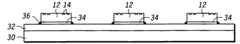
도 1을 참고하면, 본 발명의 일 실시예에 따라 형성된 패키지형 반도체 디바이스(10)의 확대 단면도가 도시된다. 패키지형 디바이스(10)는 복수의 본딩 패드(14)를 갖는 상측면을 구비한, 실리콘 웨이퍼로부터의 일 절단(one cut)과 같은 집적 회로 다이(12)를 포함한다. 본딩 패드(14)는 이에 부착된 와이어(16)를 가진다. 더욱 특히, 와이어(16)의 제1 단은 본딩 패드들(14) 각각에 접속되며, 제2 단은 볼(18)이 형성되는 공통면(패키지 저면)에 연장된다. 이하 후술되는 바와 같이, 볼(18)은 와이어본딩 프로세스의 일부로서 형성된다. 다이(12), 전기 접속, 와이어(16), 및 볼(18)의 적어도 상부는 몰드 화합물(20)로 커버 또는 캡슐화된다. 다이(12) 및 볼(18)의 하측면은 다이(12) 및 볼(18)이 인쇄 회로 기판(도시 안됨)에 접속되게 하는 땜납(22)의 박막으로 코팅된다. 와이어(16)가 접속된 볼(18)은 데이터, 파워 및 접지 신호를, 당업자에게 공지된 바와 같이, 다이(12) 및 기판 또 는 인쇄 회로 기판으로부터/에 통과시키는데 사용된다. 다이(12)가 부착되는 땜납(22)은 다이(12)로부터 열을 전도시킬 수 있으며(즉, 열 관리), 기판 레벨 땜납 조인트 강도를 강화시킨다.Referring to FIG. 1, an enlarged cross-sectional view of a packaged
집적 회로 다이(12)는 디지털 신호 프로세서, 특정 목적 회로 등과 같은 소정 타입의 회로일 수 있다. 이런 회로는 당업자에게 공지되어 있다. 와이어(16)는 패키지형 집적 회로에 공통 타입으로서 당업자에게 공지되어 있다. 와이어(16)는 전기 신호가 통과할 수 있는 전기 도전성 재료로 이루어진다. 도전성 재료는 구비, 금 또는 이들의 합금과 같은 금속일 수 있으며, 약 50 내지 100μm의 직경을 가진다. 다른 재료 및 다른 직경으로 이루어진 와이어도 또한 적합할 수 있다.Integrated circuit die 12 may be any type of circuit, such as a digital signal processor, special purpose circuits, or the like. Such circuits are known to those skilled in the art. Wire 16 is known to those skilled in the art as a type common to packaged integrated circuits. The
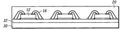
도 2A-2E 및 도 3을 참고하여, 패키지형 디바이스(10)를 형성하는 방법을 후술한다. 도 2A는 포일막(30)으로서 그 제1 측면 상에 배치된 땜납(32)의 층을 갖는 포일막(30)을 도시한 확대 단면도이다. 포일막(30)은 구리 알루미늄과 같은 비교적 평탄한 베어막(bare sheet)이다. 이런 포일막은 상용가능하며, 당업자에게 공지되어 있다. 땜납 층(32)은 포일막(30) 상에서 고온 땜납 페이스트의 층을 스크린 인쇄함에 의해 포일막(30) 상에 형성된다. 땜납(32)의 층은 약 0.1mm의 두께를 가진다. 땜납(32)은 바람직하게 약 250℃에서 300℃의 범위에서 리플로우 온도를 갖는 고온 땜납 페이스, 예컨대 약 310℃의 리플로우 온도의 97%/2%/1%Pb/Ag/Sn 땜납이다. 스테인리스 스틸 스텐실과 같은 스텐실(stencil)을 이용하여, 땜납(32)의 층은 포일막(30)의 소정 영역에 형성된다. 패키지형 집적 회로 디바이스를 형성하기 위한 프로세스의 플로우챠트인 도 3에서, 단계 50은 포일막(30)의 제공을 나타내며, 단계 52는 포일막(30) 상에서 땜납(32)의 층의 형성을 나타낸다.2A-2E and 3, a method of forming the packaged
하나 이상의 집적 회로 다이(12)는 땜납(32)에 의해 포일막(30)에 부착된다. 더욱 특히, 집적 회로 다이(12)의 제1 측면은 땜납(32)의 층에 배치된다. 땜납이 응고되기 전에 다이(12)가 땜납(32)에 배치된다면, 표준 픽 및 배치 설비(standard pick and place equipment)는 다이(12)를 포일막(30)에 부착하는데 사용될 수 있다. 다이(12)를 포일막(30) 상에서 땜납(32)에 부착하는 것을 용이하게 하기 위하여, 다이(12)의 하부 측면은 금속(34)의 층을 포함한다. 금속층(34)은 웨이퍼의 후측면이 압력하에서 웨트 연마재를 이용하여 하향 접지되는 백래핑(backlapping)을 통해, 다이(12)에 적용된다. 그 후, 금과 같은 금속은 스퍼터링을 통해 웨이퍼의 후면 상에 배치된다. 이런 후측면 금속화는 다이 부착을 용이하게 하는 것으로 공지되어 있다. 다이(12)의 상측면은 복수의 본딩 패드(14)를 포함한다.One or more integrated
도 3에서, 다이 부착은 단계 54에서 표시된다. 다음으로, 단계 56에서, 포일막(30)이 리플로우 오븐을 통과하는 제1 리플로우 프로세스가 수행된다. 오븐 내의 열은 땜납 페이스트(32)를 녹이고, 땜납은 필렛(fillet)(36)을 형성하는 다이(12)의 측면으로 조금씩 이동하여, 다이(12)를 포일막(30)에 고정시킨다.In FIG. 3, die attach is indicated in
도 3 및 2B를 참고하면, 제1 리플로우 프로세스(56) 이후, 본딩 패드(14)를 포일막(30)에 접속시키는 와이어(16)가 부착되는 와이어 본딩 단계 58가 수행된다. 와이어(16)는 본딩 패드(14)를 포일막(30) 상의 땜납(32)에 접속시킨다. 당업자가 이해할 수 있는 바와 같이, 땜납(32)은 포일막(30)의 소정 위치, 예컨대, 다이(12)를 수용하도록 결정된 위치, 및 패키지형 디바이스(10) 입력 및 출력에 대해 정의 된 위치로서, 본 예에서는 랜드 그리드 어레이(land grid array)(도 4 참조)에 대해 형성된다. 와이어 본딩 프로세스는 바람직하게 볼 본딩 프로세스이다. 공지된 볼 본딩 프로세스에서, 와이어는 캐필러리(capillary)에 유지되며, EFO(elctrical spark)는 와이어의 팁에서 매우 작은 볼을 형성하는데 사용된다. 본 발명에서, 와이어(16)의 가열된 팁은 포일막(30) 상에 땜납(32)에 가압된다. 와이어(16)의 팁이 뜨겁기 때문에, 소프트해져서, 스쿼시드(squashed) 볼(38)은 포일막(30) 상에 형성된다. 각종 게이지 와이어는 다이(12)의 전기적 요건에 따라 사용될 수 있다. 전형적인 와이어 크기는 약 50μm 내지 100μm 사이에 있다. 75μm 게이지 와이어에서, 스쿼시드 볼 본드는 약 0.25mm의 직경을 가진다. 더욱이, 평편한 포일막이 사용되기 때문에, 볼(38)은 실질적으로 평편한 저면을 가진다. 회로 I/O의 수는 와이어(16) 및 볼(38)의 수를 결정하는데 사용된다.3 and 2B, after the
와이어본딩 프로세스(58)가 수행된 후, 다이(12), 전기 접속, 와이어(16) 및 볼(38)의 일부는 바람직하게 집적 회로를 패키징하는 분야에서 공지된 플라스틱 재료로 캡슐화된다. 도 2C 및 3에서 단계 60은 다이(12), 와이어(16), 및 땜납(32) 층 및 포일막(30)의 상부들 상에 몰드 화합물(20)이 형성되는 단계를 예시한다. 바람직한 몰드 화합물(20)은 반도체 패키징에서 사용되는 일반적으로 상용가능한 에폭시 몰딩 화합물이다. 도 2C는 캡슐재(20)를 갖는 포일막을 도시한다. 이런 스테이지에서, 캡슐재(20)는 포일막(30)의 일 측면 전체를 커버한다.After the
캡슐화 단계(60) 이후, 제2 리플로우 프로세스(62)는 다이(12) 및 와이어(16)로부터 포일막(30)을 분리하도록 수행된다. 도 2D는 캡슐화된 다이(12) 및 와이어(16)로부터 분리된 땜납(32) 층의 일부 및 포일막(30)을 도시한다. 제2 리플로우 프로세스(62)는 금속 포일(30) 상에서 땜납(32)을 평활화하며, 에폭시 몰드 화합물(20)과 금속 포일(30) 사이의 인터페이스를 약하게 하여, 몰드 화합물(20)로부터 포일막(30)의 탈착을 용이하게 한다. 와이어(16) 및 다이(12)로부터 분리된 후 땜납(32)의 일부가 포일막(30)에 부착된 채 유지됨에 유의해야 한다.After
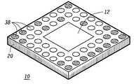
전형적인 패키징 프로세스가 다수의 디바이스를 실질적으로 동시에 패키징할 때, 포일막(30)이 탈착된 후, 캡슐화된 다이(12), 및 각 다이에 접속된 와이어(16)는 서로 분리되어, 다수의 패키지형 디바이스(10)는 싱귤레이션(singulation) 단계 64에 있게 한다. 도 2E는 싱귤레이션 이후 3개의 개별 디바이스(10)를 도시한다. 공지된 쏘 싱귤레이션(saw singulation) 프로세스가 바람직하다. 도 4는 본 발명의 방법에 따라 형성된 패키지형 디바이스(10)의 확대 저부 사시도이다.When a typical packaging process packages multiple devices substantially simultaneously, after the
쏘 싱귤레이션 프로세스(64) 이전에, 선택적인 전기 기능 테스트가 수행된다. 캡슐화된 디바이스의 모든 I/O 단자가 패키징 프로세스를 통해 분리되기 때문에, 스트립 형태의 전기 테스트는 가능하여, 부가 프로세스 또는 비용 없이도 테스터 활용을 개선하고 병렬 테스팅을 가능하게 한다.Prior to the
패키지형 디바이스(10)는 IC(12)로부터 기판까지의 신호 경로가 짧기 때문에 개선된 고 주파수 전기 성능을 가진다. 더욱이, 시스템 신뢰도는 시스템 기판의 열화에 의해 야기된 스트레스 고장에 대한 땜납 조인트 내성을 증가시킴에 의해 개선된다. 개선된 RF 성능 및 기계적 스트레스 고장에 대한 내성은 셀룰러 전화 핸드셋 제작자에게는 매우 중요한 문제가 된다.Packaged
본 발명은 또한 MCM(multi-chip module), SIP(system in a package), 및 스택형(stacked) 다이 디바이스를 형성하는데 사용될 수 있다. 도 5는 전술한 방법에 따라 형성된 수동 디바이스(44) 및 2개의 집적 회로(42)를 구비한 멀티 칩 디바이스(40)를 도시한다. 회로(42) 및 수동 디바이스(44)는 와이어(46)와 접속된다. 회로(42 및 44) 및 와이어(46)는 몰드 화합물(48)로 캡슐화된다. 전술한 바와 같이, 땜납의 소량이 와이어(46)의 단부 및 회로(42 및 44)의 아래에 형성된 스쿼시드 볼 상에 남는다.The invention may also be used to form multi-chip modules (MCMs), system in a package (SIP), and stacked die devices. 5 shows a
비록 실시예에 패키지형 디바이스가 노출된 다이형 디바이스로 도시되었다 할지라도, 본 발명은 히트 싱크를 갖추고 히트 싱크가 노출된 패키지형 디바이스에 적용될 수 있다. 이 경우, 다이(12)는 구리와 같은 금속으로 이루어진 다이 패들의 일 측면에 부착되며, 다이 패들의 다른 측면은 포일막에 부착된다.Although the packaged device in the embodiment is shown as an exposed die type device, the present invention can be applied to a packaged device having a heat sink and having a heat sink exposed. In this case, the
본 발명은 집적 회로를 패키징하는 용이하고 값싼 방법을 제공한다. 디바이스 비용은 기판 또는 종단(외부 핀 또는 볼) 모두가 요구되지 않기 때문에, 낮게 된다. 금속 리드프레임이 없기 때문에, 싱귤레이션 단계에서 사용되는 쏘 블레이드는 금속을 절단할 필요가 없으며, 이에 따라 쏘 블레이드는 더 긴 수명을 가진다. 또한, 리드프레임이 요구되지 않기 때문에, 기판 트레이스 라우팅을 수행할 필요가 없다. 패키징 프로세스는 값비싼 어떤 화학적 에치-백을 요구하지 않는다. 패키징 프로세스는 현재 이용가능한 설비를 이용하여 수행될 수 있다. 패키지는 또한 0.4mm로 낮춘 매우 낮은 프로파일을 가진다. 랜드 그리드 어레이는 고 상호접속 밀도를 제공한다. 예컨대, 200+I/O가 가능하다.The present invention provides an easy and inexpensive method of packaging an integrated circuit. Device cost is low because neither the substrate nor the termination (outer pin or ball) is required. Since there is no metal leadframe, the saw blade used in the singulation step does not need to cut metal, so the saw blade has a longer life. In addition, since no leadframe is required, there is no need to perform substrate trace routing. The packaging process does not require any expensive chemical etch-back. The packaging process can be performed using the equipment currently available. The package also has a very low profile down to 0.4mm. Land grid arrays provide high interconnect density. For example, 200 + I / O is possible.
본 발명의 바람직한 실시예가 예시되고 설명되었다 할지라도, 본 발명은 이들 실시예에만 제한되지 않는다. 수많은 수정, 변화, 변형, 대체 및 균등물이 당업자에게는 첨부된 특허청구범위의 정신 및 범위를 벗어남이 없이 자명하게 이해될 것이다.Although the preferred embodiments of the invention have been illustrated and described, the invention is not limited to these embodiments. Numerous modifications, changes, variations, substitutions and equivalents will be apparent to those skilled in the art without departing from the spirit and scope of the appended claims.
Claims (20)
Translated fromKoreanApplications Claiming Priority (2)
| Application Number | Priority Date | Filing Date | Title |
|---|---|---|---|
| US10/807,527US7205178B2 (en) | 2004-03-24 | 2004-03-24 | Land grid array packaged device and method of forming same |
| US10/807,527 | 2004-03-24 |
Publications (1)
| Publication Number | Publication Date |
|---|---|
| KR20070007151Atrue KR20070007151A (en) | 2007-01-12 |
Family
ID=34990515
Family Applications (1)
| Application Number | Title | Priority Date | Filing Date |
|---|---|---|---|
| KR1020067021940AWithdrawnKR20070007151A (en) | 2004-03-24 | 2005-02-10 | Land grid array packaged device and method of forming the same |
Country Status (6)
| Country | Link |
|---|---|
| US (1) | US7205178B2 (en) |
| JP (1) | JP5079493B2 (en) |
| KR (1) | KR20070007151A (en) |
| CN (1) | CN100499052C (en) |
| TW (1) | TWI349985B (en) |
| WO (1) | WO2005104211A2 (en) |
Cited By (1)
| Publication number | Priority date | Publication date | Assignee | Title |
|---|---|---|---|---|
| KR20150079592A (en)* | 2012-09-07 | 2015-07-08 | 이오플렉스 리미티드 | Lead carrier with print-formed terminal pads |
Families Citing this family (46)
| Publication number | Priority date | Publication date | Assignee | Title |
|---|---|---|---|---|
| TWI231578B (en)* | 2003-12-01 | 2005-04-21 | Advanced Semiconductor Eng | Anti-warpage package and method for making the same |
| US20060134828A1 (en)* | 2004-12-17 | 2006-06-22 | Texas Instruments Incorporated | Package that integrates passive and active devices with or without a lead frame |
| US20060170081A1 (en)* | 2005-02-03 | 2006-08-03 | Gerber Mark A | Method and apparatus for packaging an electronic chip |
| JP5001542B2 (en)* | 2005-03-17 | 2012-08-15 | 日立電線株式会社 | Electronic device substrate, method for manufacturing the same, and method for manufacturing the electronic device |
| US20070216033A1 (en)* | 2006-03-20 | 2007-09-20 | Corisis David J | Carrierless chip package for integrated circuit devices, and methods of making same |
| US8461694B1 (en) | 2006-04-28 | 2013-06-11 | Utac Thai Limited | Lead frame ball grid array with traces under die having interlocking features |
| US8310060B1 (en) | 2006-04-28 | 2012-11-13 | Utac Thai Limited | Lead frame land grid array |
| US8460970B1 (en) | 2006-04-28 | 2013-06-11 | Utac Thai Limited | Lead frame ball grid array with traces under die having interlocking features |
| US8492906B2 (en)* | 2006-04-28 | 2013-07-23 | Utac Thai Limited | Lead frame ball grid array with traces under die |
| US8487451B2 (en)* | 2006-04-28 | 2013-07-16 | Utac Thai Limited | Lead frame land grid array with routing connector trace under unit |
| US8125077B2 (en)* | 2006-09-26 | 2012-02-28 | Utac Thai Limited | Package with heat transfer |
| US8013437B1 (en) | 2006-09-26 | 2011-09-06 | Utac Thai Limited | Package with heat transfer |
| US9761435B1 (en) | 2006-12-14 | 2017-09-12 | Utac Thai Limited | Flip chip cavity package |
| US9082607B1 (en) | 2006-12-14 | 2015-07-14 | Utac Thai Limited | Molded leadframe substrate semiconductor package |
| US8188596B2 (en) | 2007-02-09 | 2012-05-29 | Infineon Technologies Ag | Multi-chip module |
| JP2008282853A (en)* | 2007-05-08 | 2008-11-20 | Spansion Llc | Semiconductor device and its manufacturing process |
| US7790512B1 (en) | 2007-11-06 | 2010-09-07 | Utac Thai Limited | Molded leadframe substrate semiconductor package |
| US8063470B1 (en)* | 2008-05-22 | 2011-11-22 | Utac Thai Limited | Method and apparatus for no lead semiconductor package |
| US9947605B2 (en)* | 2008-09-04 | 2018-04-17 | UTAC Headquarters Pte. Ltd. | Flip chip cavity package |
| JP5588150B2 (en)* | 2009-02-06 | 2014-09-10 | セイコーインスツル株式会社 | Resin-sealed semiconductor device |
| US8569877B2 (en)* | 2009-03-12 | 2013-10-29 | Utac Thai Limited | Metallic solderability preservation coating on metal part of semiconductor package to prevent oxide |
| US8097956B2 (en)* | 2009-03-12 | 2012-01-17 | Apple Inc. | Flexible packaging for chip-on-chip and package-on-package technologies |
| US9449900B2 (en) | 2009-07-23 | 2016-09-20 | UTAC Headquarters Pte. Ltd. | Leadframe feature to minimize flip-chip semiconductor die collapse during flip-chip reflow |
| US9355940B1 (en) | 2009-12-04 | 2016-05-31 | Utac Thai Limited | Auxiliary leadframe member for stabilizing the bond wire process |
| US8368189B2 (en)* | 2009-12-04 | 2013-02-05 | Utac Thai Limited | Auxiliary leadframe member for stabilizing the bond wire process |
| TWI392066B (en)* | 2009-12-28 | 2013-04-01 | 矽品精密工業股份有限公司 | Package structure and fabrication method thereof |
| US8575732B2 (en) | 2010-03-11 | 2013-11-05 | Utac Thai Limited | Leadframe based multi terminal IC package |
| US8871571B2 (en) | 2010-04-02 | 2014-10-28 | Utac Thai Limited | Apparatus for and methods of attaching heat slugs to package tops |
| JP5642473B2 (en)* | 2010-09-22 | 2014-12-17 | セイコーインスツル株式会社 | BGA semiconductor package and manufacturing method thereof |
| US9029198B2 (en) | 2012-05-10 | 2015-05-12 | Utac Thai Limited | Methods of manufacturing semiconductor devices including terminals with internal routing interconnections |
| US9449905B2 (en) | 2012-05-10 | 2016-09-20 | Utac Thai Limited | Plated terminals with routing interconnections semiconductor device |
| US9006034B1 (en) | 2012-06-11 | 2015-04-14 | Utac Thai Limited | Post-mold for semiconductor package having exposed traces |
| CN102832141A (en)* | 2012-08-18 | 2012-12-19 | 孙青秀 | Manufacturing process of carrier-free package based on framework |
| TWI476879B (en)* | 2012-11-21 | 2015-03-11 | Powertech Technology Inc | Land grid array package and its substrate |
| US9437458B2 (en) | 2013-11-12 | 2016-09-06 | Infineon Technologies Ag | Method of electrically isolating leads of a lead frame strip |
| US9324642B2 (en)* | 2013-11-12 | 2016-04-26 | Infineon Technologies Ag | Method of electrically isolating shared leads of a lead frame strip |
| US9287238B2 (en) | 2013-12-02 | 2016-03-15 | Infineon Technologies Ag | Leadless semiconductor package with optical inspection feature |
| US10242953B1 (en) | 2015-05-27 | 2019-03-26 | Utac Headquarters PTE. Ltd | Semiconductor package with plated metal shielding and a method thereof |
| US10242934B1 (en) | 2014-05-07 | 2019-03-26 | Utac Headquarters Pte Ltd. | Semiconductor package with full plating on contact side surfaces and methods thereof |
| US9252063B2 (en) | 2014-07-07 | 2016-02-02 | Infineon Technologies Ag | Extended contact area for leadframe strip testing |
| US20180047588A1 (en)* | 2015-05-04 | 2018-02-15 | Eoplex Limited | Lead carrier structure and packages formed therefrom without die attach pads |
| US9842831B2 (en)* | 2015-05-14 | 2017-12-12 | Mediatek Inc. | Semiconductor package and fabrication method thereof |
| US10685943B2 (en) | 2015-05-14 | 2020-06-16 | Mediatek Inc. | Semiconductor chip package with resilient conductive paste post and fabrication method thereof |
| US9917038B1 (en) | 2015-11-10 | 2018-03-13 | Utac Headquarters Pte Ltd | Semiconductor package with multiple molding routing layers and a method of manufacturing the same |
| US10276477B1 (en) | 2016-05-20 | 2019-04-30 | UTAC Headquarters Pte. Ltd. | Semiconductor package with multiple stacked leadframes and a method of manufacturing the same |
| IT201700073501A1 (en)* | 2017-06-30 | 2018-12-30 | St Microelectronics Srl | SEMICONDUCTOR PRODUCT AND CORRESPONDENT PROCEDURE |
Family Cites Families (18)
| Publication number | Priority date | Publication date | Assignee | Title |
|---|---|---|---|---|
| JPS59208756A (en)* | 1983-05-12 | 1984-11-27 | Sony Corp | Manufacture of semiconductor device package |
| US5200362A (en)* | 1989-09-06 | 1993-04-06 | Motorola, Inc. | Method of attaching conductive traces to an encapsulated semiconductor die using a removable transfer film |
| KR930024126A (en)* | 1992-05-12 | 1993-12-22 | 아키라 기타하라 | Surface Mount Devices and Their Semifinished Products |
| JP2595909B2 (en)* | 1994-09-14 | 1997-04-02 | 日本電気株式会社 | Semiconductor device |
| US6376921B1 (en)* | 1995-11-08 | 2002-04-23 | Fujitsu Limited | Semiconductor device, method for fabricating the semiconductor device, lead frame and method for producing the lead frame |
| JP3207738B2 (en)* | 1996-01-15 | 2001-09-10 | 株式会社東芝 | Resin-sealed semiconductor device and method of manufacturing the same |
| JP3639390B2 (en)* | 1996-10-17 | 2005-04-20 | 三洋電機株式会社 | Semiconductor device |
| US6498099B1 (en)* | 1998-06-10 | 2002-12-24 | Asat Ltd. | Leadless plastic chip carrier with etch back pad singulation |
| JP2000332150A (en)* | 1999-05-20 | 2000-11-30 | Fujitsu Ltd | Method for manufacturing semiconductor device |
| JP3883784B2 (en)* | 2000-05-24 | 2007-02-21 | 三洋電機株式会社 | Plate-shaped body and method for manufacturing semiconductor device |
| US6528892B2 (en)* | 2001-06-05 | 2003-03-04 | International Business Machines Corporation | Land grid array stiffener use with flexible chip carriers |
| JP4014912B2 (en)* | 2001-09-28 | 2007-11-28 | 株式会社ルネサステクノロジ | Semiconductor device |
| US6711026B2 (en)* | 2001-11-13 | 2004-03-23 | International Business Machines Corporation | Sash for land grid arrays |
| US7323767B2 (en)* | 2002-04-25 | 2008-01-29 | Micron Technology, Inc. | Standoffs for centralizing internals in packaging process |
| US6965160B2 (en)* | 2002-08-15 | 2005-11-15 | Micron Technology, Inc. | Semiconductor dice packages employing at least one redistribution layer |
| JP2004119726A (en)* | 2002-09-26 | 2004-04-15 | Sanyo Electric Co Ltd | Method of manufacturing circuit device |
| US6917090B2 (en)* | 2003-04-07 | 2005-07-12 | Micron Technology, Inc. | Chip scale image sensor package |
| JP2005203497A (en)* | 2004-01-14 | 2005-07-28 | Toshiba Corp | Semiconductor device and manufacturing method thereof |
- 2004
- 2004-03-24USUS10/807,527patent/US7205178B2/ennot_activeExpired - Fee Related
- 2005
- 2005-01-28TWTW094102718Apatent/TWI349985B/ennot_activeIP Right Cessation
- 2005-02-10WOPCT/US2005/004006patent/WO2005104211A2/enactiveApplication Filing
- 2005-02-10KRKR1020067021940Apatent/KR20070007151A/ennot_activeWithdrawn
- 2005-02-10CNCNB2005800092962Apatent/CN100499052C/ennot_activeExpired - Fee Related
- 2005-02-10JPJP2007504955Apatent/JP5079493B2/ennot_activeExpired - Fee Related
Cited By (1)
| Publication number | Priority date | Publication date | Assignee | Title |
|---|---|---|---|---|
| KR20150079592A (en)* | 2012-09-07 | 2015-07-08 | 이오플렉스 리미티드 | Lead carrier with print-formed terminal pads |
Also Published As
| Publication number | Publication date |
|---|---|
| US20050214980A1 (en) | 2005-09-29 |
| CN101006570A (en) | 2007-07-25 |
| WO2005104211A2 (en) | 2005-11-03 |
| JP2007531270A (en) | 2007-11-01 |
| CN100499052C (en) | 2009-06-10 |
| TWI349985B (en) | 2011-10-01 |
| US7205178B2 (en) | 2007-04-17 |
| WO2005104211A3 (en) | 2006-01-19 |
| TW200537672A (en) | 2005-11-16 |
| JP5079493B2 (en) | 2012-11-21 |
Similar Documents
| Publication | Publication Date | Title |
|---|---|---|
| CN100499052C (en) | Planar grid array packaging device and manufacturing method thereof | |
| US6406938B2 (en) | Semiconductor and flip chip packages and method having a back-side connection | |
| US7915077B2 (en) | Methods of making metal core foldover package structures | |
| US7704800B2 (en) | Semiconductor assembly with one metal layer after base metal removal | |
| US7285855B2 (en) | Packaged device and method of forming same | |
| US9269695B2 (en) | Semiconductor device assemblies including face-to-face semiconductor dice and related methods | |
| TWI482261B (en) | Three-dimensional system-in-package package-on-package structure | |
| US7378298B2 (en) | Method of making stacked die package | |
| KR101119708B1 (en) | Land grid array packaged device and method of forming same | |
| US6841884B2 (en) | Semiconductor device | |
| US7696618B2 (en) | POP (package-on-package) semiconductor device | |
| US20100289145A1 (en) | Wafer chip scale package with center conductive mass | |
| CN101266966B (en) | Multi-chip package module and manufacturing method thereof | |
| US7179682B2 (en) | Packaged device and method of forming same | |
| US20070281393A1 (en) | Method of forming a trace embedded package | |
| JP2002261192A (en) | Wafer level csp | |
| KR100737217B1 (en) | Substrateless flip chip package and manufacturing method thereof | |
| Lin et al. | 3D stackable packages with bumpless interconnect technology | |
| JPH1167985A (en) | Semiconductor device | |
| KR20010060879A (en) | Ball grid array package and manufacturing method thereof | |
| TW201005914A (en) | Semiconductor package structure |
Legal Events
| Date | Code | Title | Description |
|---|---|---|---|
| PA0105 | International application | Patent event date:20061023 Patent event code:PA01051R01D Comment text:International Patent Application | |
| PG1501 | Laying open of application | ||
| PC1203 | Withdrawal of no request for examination | ||
| WITN | Application deemed withdrawn, e.g. because no request for examination was filed or no examination fee was paid |