KR20060124532A - Semiconductor device and manufacturing method thereof - Google Patents
Semiconductor device and manufacturing method thereofDownload PDFInfo
- Publication number
- KR20060124532A KR20060124532AKR1020050083036AKR20050083036AKR20060124532AKR 20060124532 AKR20060124532 AKR 20060124532AKR 1020050083036 AKR1020050083036 AKR 1020050083036AKR 20050083036 AKR20050083036 AKR 20050083036AKR 20060124532 AKR20060124532 AKR 20060124532A
- Authority
- KR
- South Korea
- Prior art keywords
- conductor layer
- layer
- semiconductor element
- columnar
- frame member
- Prior art date
- Legal status (The legal status is an assumption and is not a legal conclusion. Google has not performed a legal analysis and makes no representation as to the accuracy of the status listed.)
- Granted
Links
Images


Classifications
- H—ELECTRICITY
- H01—ELECTRIC ELEMENTS
- H01L—SEMICONDUCTOR DEVICES NOT COVERED BY CLASS H10
- H01L24/00—Arrangements for connecting or disconnecting semiconductor or solid-state bodies; Methods or apparatus related thereto
- H01L24/01—Means for bonding being attached to, or being formed on, the surface to be connected, e.g. chip-to-package, die-attach, "first-level" interconnects; Manufacturing methods related thereto
- H01L24/02—Bonding areas ; Manufacturing methods related thereto
- H01L24/04—Structure, shape, material or disposition of the bonding areas prior to the connecting process
- H01L24/05—Structure, shape, material or disposition of the bonding areas prior to the connecting process of an individual bonding area
- H—ELECTRICITY
- H01—ELECTRIC ELEMENTS
- H01L—SEMICONDUCTOR DEVICES NOT COVERED BY CLASS H10
- H01L24/00—Arrangements for connecting or disconnecting semiconductor or solid-state bodies; Methods or apparatus related thereto
- H01L24/01—Means for bonding being attached to, or being formed on, the surface to be connected, e.g. chip-to-package, die-attach, "first-level" interconnects; Manufacturing methods related thereto
- H01L24/02—Bonding areas ; Manufacturing methods related thereto
- H01L24/03—Manufacturing methods
- H—ELECTRICITY
- H01—ELECTRIC ELEMENTS
- H01L—SEMICONDUCTOR DEVICES NOT COVERED BY CLASS H10
- H01L24/00—Arrangements for connecting or disconnecting semiconductor or solid-state bodies; Methods or apparatus related thereto
- H01L24/01—Means for bonding being attached to, or being formed on, the surface to be connected, e.g. chip-to-package, die-attach, "first-level" interconnects; Manufacturing methods related thereto
- H01L24/42—Wire connectors; Manufacturing methods related thereto
- H01L24/47—Structure, shape, material or disposition of the wire connectors after the connecting process
- H01L24/48—Structure, shape, material or disposition of the wire connectors after the connecting process of an individual wire connector
- H—ELECTRICITY
- H01—ELECTRIC ELEMENTS
- H01L—SEMICONDUCTOR DEVICES NOT COVERED BY CLASS H10
- H01L2224/00—Indexing scheme for arrangements for connecting or disconnecting semiconductor or solid-state bodies and methods related thereto as covered by H01L24/00
- H01L2224/01—Means for bonding being attached to, or being formed on, the surface to be connected, e.g. chip-to-package, die-attach, "first-level" interconnects; Manufacturing methods related thereto
- H01L2224/02—Bonding areas; Manufacturing methods related thereto
- H01L2224/0212—Auxiliary members for bonding areas, e.g. spacers
- H01L2224/02122—Auxiliary members for bonding areas, e.g. spacers being formed on the semiconductor or solid-state body
- H01L2224/02163—Auxiliary members for bonding areas, e.g. spacers being formed on the semiconductor or solid-state body on the bonding area
- H01L2224/02165—Reinforcing structures
- H01L2224/02166—Collar structures
- H—ELECTRICITY
- H01—ELECTRIC ELEMENTS
- H01L—SEMICONDUCTOR DEVICES NOT COVERED BY CLASS H10
- H01L2224/00—Indexing scheme for arrangements for connecting or disconnecting semiconductor or solid-state bodies and methods related thereto as covered by H01L24/00
- H01L2224/01—Means for bonding being attached to, or being formed on, the surface to be connected, e.g. chip-to-package, die-attach, "first-level" interconnects; Manufacturing methods related thereto
- H01L2224/02—Bonding areas; Manufacturing methods related thereto
- H01L2224/04—Structure, shape, material or disposition of the bonding areas prior to the connecting process
- H01L2224/04042—Bonding areas specifically adapted for wire connectors, e.g. wirebond pads
- H—ELECTRICITY
- H01—ELECTRIC ELEMENTS
- H01L—SEMICONDUCTOR DEVICES NOT COVERED BY CLASS H10
- H01L2224/00—Indexing scheme for arrangements for connecting or disconnecting semiconductor or solid-state bodies and methods related thereto as covered by H01L24/00
- H01L2224/01—Means for bonding being attached to, or being formed on, the surface to be connected, e.g. chip-to-package, die-attach, "first-level" interconnects; Manufacturing methods related thereto
- H01L2224/02—Bonding areas; Manufacturing methods related thereto
- H01L2224/04—Structure, shape, material or disposition of the bonding areas prior to the connecting process
- H01L2224/05—Structure, shape, material or disposition of the bonding areas prior to the connecting process of an individual bonding area
- H01L2224/05001—Internal layers
- H01L2224/05075—Plural internal layers
- H01L2224/0508—Plural internal layers being stacked
- H01L2224/05085—Plural internal layers being stacked with additional elements, e.g. vias arrays, interposed between the stacked layers
- H01L2224/05089—Disposition of the additional element
- H01L2224/05093—Disposition of the additional element of a plurality of vias
- H01L2224/05095—Disposition of the additional element of a plurality of vias at the periphery of the internal layers
- H—ELECTRICITY
- H01—ELECTRIC ELEMENTS
- H01L—SEMICONDUCTOR DEVICES NOT COVERED BY CLASS H10
- H01L2224/00—Indexing scheme for arrangements for connecting or disconnecting semiconductor or solid-state bodies and methods related thereto as covered by H01L24/00
- H01L2224/01—Means for bonding being attached to, or being formed on, the surface to be connected, e.g. chip-to-package, die-attach, "first-level" interconnects; Manufacturing methods related thereto
- H01L2224/02—Bonding areas; Manufacturing methods related thereto
- H01L2224/04—Structure, shape, material or disposition of the bonding areas prior to the connecting process
- H01L2224/05—Structure, shape, material or disposition of the bonding areas prior to the connecting process of an individual bonding area
- H01L2224/05001—Internal layers
- H01L2224/05075—Plural internal layers
- H01L2224/0508—Plural internal layers being stacked
- H01L2224/05085—Plural internal layers being stacked with additional elements, e.g. vias arrays, interposed between the stacked layers
- H01L2224/05089—Disposition of the additional element
- H01L2224/05093—Disposition of the additional element of a plurality of vias
- H01L2224/05096—Uniform arrangement, i.e. array
- H—ELECTRICITY
- H01—ELECTRIC ELEMENTS
- H01L—SEMICONDUCTOR DEVICES NOT COVERED BY CLASS H10
- H01L2224/00—Indexing scheme for arrangements for connecting or disconnecting semiconductor or solid-state bodies and methods related thereto as covered by H01L24/00
- H01L2224/01—Means for bonding being attached to, or being formed on, the surface to be connected, e.g. chip-to-package, die-attach, "first-level" interconnects; Manufacturing methods related thereto
- H01L2224/02—Bonding areas; Manufacturing methods related thereto
- H01L2224/04—Structure, shape, material or disposition of the bonding areas prior to the connecting process
- H01L2224/05—Structure, shape, material or disposition of the bonding areas prior to the connecting process of an individual bonding area
- H01L2224/0554—External layer
- H01L2224/0555—Shape
- H01L2224/05552—Shape in top view
- H01L2224/05554—Shape in top view being square
- H—ELECTRICITY
- H01—ELECTRIC ELEMENTS
- H01L—SEMICONDUCTOR DEVICES NOT COVERED BY CLASS H10
- H01L2224/00—Indexing scheme for arrangements for connecting or disconnecting semiconductor or solid-state bodies and methods related thereto as covered by H01L24/00
- H01L2224/01—Means for bonding being attached to, or being formed on, the surface to be connected, e.g. chip-to-package, die-attach, "first-level" interconnects; Manufacturing methods related thereto
- H01L2224/02—Bonding areas; Manufacturing methods related thereto
- H01L2224/04—Structure, shape, material or disposition of the bonding areas prior to the connecting process
- H01L2224/05—Structure, shape, material or disposition of the bonding areas prior to the connecting process of an individual bonding area
- H01L2224/0554—External layer
- H01L2224/05599—Material
- H01L2224/056—Material with a principal constituent of the material being a metal or a metalloid, e.g. boron [B], silicon [Si], germanium [Ge], arsenic [As], antimony [Sb], tellurium [Te] and polonium [Po], and alloys thereof
- H01L2224/05617—Material with a principal constituent of the material being a metal or a metalloid, e.g. boron [B], silicon [Si], germanium [Ge], arsenic [As], antimony [Sb], tellurium [Te] and polonium [Po], and alloys thereof the principal constituent melting at a temperature of greater than or equal to 400°C and less than 950°C
- H01L2224/05624—Aluminium [Al] as principal constituent
- H—ELECTRICITY
- H01—ELECTRIC ELEMENTS
- H01L—SEMICONDUCTOR DEVICES NOT COVERED BY CLASS H10
- H01L2224/00—Indexing scheme for arrangements for connecting or disconnecting semiconductor or solid-state bodies and methods related thereto as covered by H01L24/00
- H01L2224/01—Means for bonding being attached to, or being formed on, the surface to be connected, e.g. chip-to-package, die-attach, "first-level" interconnects; Manufacturing methods related thereto
- H01L2224/42—Wire connectors; Manufacturing methods related thereto
- H01L2224/47—Structure, shape, material or disposition of the wire connectors after the connecting process
- H01L2224/48—Structure, shape, material or disposition of the wire connectors after the connecting process of an individual wire connector
- H01L2224/484—Connecting portions
- H01L2224/48463—Connecting portions the connecting portion on the bonding area of the semiconductor or solid-state body being a ball bond
- H—ELECTRICITY
- H01—ELECTRIC ELEMENTS
- H01L—SEMICONDUCTOR DEVICES NOT COVERED BY CLASS H10
- H01L2224/00—Indexing scheme for arrangements for connecting or disconnecting semiconductor or solid-state bodies and methods related thereto as covered by H01L24/00
- H01L2224/01—Means for bonding being attached to, or being formed on, the surface to be connected, e.g. chip-to-package, die-attach, "first-level" interconnects; Manufacturing methods related thereto
- H01L2224/42—Wire connectors; Manufacturing methods related thereto
- H01L2224/47—Structure, shape, material or disposition of the wire connectors after the connecting process
- H01L2224/49—Structure, shape, material or disposition of the wire connectors after the connecting process of a plurality of wire connectors
- H01L2224/491—Disposition
- H01L2224/4912—Layout
- H01L2224/49171—Fan-out arrangements
- H—ELECTRICITY
- H01—ELECTRIC ELEMENTS
- H01L—SEMICONDUCTOR DEVICES NOT COVERED BY CLASS H10
- H01L2224/00—Indexing scheme for arrangements for connecting or disconnecting semiconductor or solid-state bodies and methods related thereto as covered by H01L24/00
- H01L2224/80—Methods for connecting semiconductor or other solid state bodies using means for bonding being attached to, or being formed on, the surface to be connected
- H01L2224/85—Methods for connecting semiconductor or other solid state bodies using means for bonding being attached to, or being formed on, the surface to be connected using a wire connector
- H01L2224/8538—Bonding interfaces outside the semiconductor or solid-state body
- H01L2224/85399—Material
- H—ELECTRICITY
- H01—ELECTRIC ELEMENTS
- H01L—SEMICONDUCTOR DEVICES NOT COVERED BY CLASS H10
- H01L24/00—Arrangements for connecting or disconnecting semiconductor or solid-state bodies; Methods or apparatus related thereto
- H01L24/01—Means for bonding being attached to, or being formed on, the surface to be connected, e.g. chip-to-package, die-attach, "first-level" interconnects; Manufacturing methods related thereto
- H01L24/42—Wire connectors; Manufacturing methods related thereto
- H01L24/47—Structure, shape, material or disposition of the wire connectors after the connecting process
- H01L24/49—Structure, shape, material or disposition of the wire connectors after the connecting process of a plurality of wire connectors
- H—ELECTRICITY
- H01—ELECTRIC ELEMENTS
- H01L—SEMICONDUCTOR DEVICES NOT COVERED BY CLASS H10
- H01L2924/00—Indexing scheme for arrangements or methods for connecting or disconnecting semiconductor or solid-state bodies as covered by H01L24/00
- H01L2924/0001—Technical content checked by a classifier
- H01L2924/00014—Technical content checked by a classifier the subject-matter covered by the group, the symbol of which is combined with the symbol of this group, being disclosed without further technical details
- H—ELECTRICITY
- H01—ELECTRIC ELEMENTS
- H01L—SEMICONDUCTOR DEVICES NOT COVERED BY CLASS H10
- H01L2924/00—Indexing scheme for arrangements or methods for connecting or disconnecting semiconductor or solid-state bodies as covered by H01L24/00
- H01L2924/01—Chemical elements
- H01L2924/01004—Beryllium [Be]
- H—ELECTRICITY
- H01—ELECTRIC ELEMENTS
- H01L—SEMICONDUCTOR DEVICES NOT COVERED BY CLASS H10
- H01L2924/00—Indexing scheme for arrangements or methods for connecting or disconnecting semiconductor or solid-state bodies as covered by H01L24/00
- H01L2924/01—Chemical elements
- H01L2924/01006—Carbon [C]
- H—ELECTRICITY
- H01—ELECTRIC ELEMENTS
- H01L—SEMICONDUCTOR DEVICES NOT COVERED BY CLASS H10
- H01L2924/00—Indexing scheme for arrangements or methods for connecting or disconnecting semiconductor or solid-state bodies as covered by H01L24/00
- H01L2924/01—Chemical elements
- H01L2924/01013—Aluminum [Al]
- H—ELECTRICITY
- H01—ELECTRIC ELEMENTS
- H01L—SEMICONDUCTOR DEVICES NOT COVERED BY CLASS H10
- H01L2924/00—Indexing scheme for arrangements or methods for connecting or disconnecting semiconductor or solid-state bodies as covered by H01L24/00
- H01L2924/01—Chemical elements
- H01L2924/01014—Silicon [Si]
- H—ELECTRICITY
- H01—ELECTRIC ELEMENTS
- H01L—SEMICONDUCTOR DEVICES NOT COVERED BY CLASS H10
- H01L2924/00—Indexing scheme for arrangements or methods for connecting or disconnecting semiconductor or solid-state bodies as covered by H01L24/00
- H01L2924/01—Chemical elements
- H01L2924/01019—Potassium [K]
- H—ELECTRICITY
- H01—ELECTRIC ELEMENTS
- H01L—SEMICONDUCTOR DEVICES NOT COVERED BY CLASS H10
- H01L2924/00—Indexing scheme for arrangements or methods for connecting or disconnecting semiconductor or solid-state bodies as covered by H01L24/00
- H01L2924/01—Chemical elements
- H01L2924/01022—Titanium [Ti]
- H—ELECTRICITY
- H01—ELECTRIC ELEMENTS
- H01L—SEMICONDUCTOR DEVICES NOT COVERED BY CLASS H10
- H01L2924/00—Indexing scheme for arrangements or methods for connecting or disconnecting semiconductor or solid-state bodies as covered by H01L24/00
- H01L2924/01—Chemical elements
- H01L2924/01029—Copper [Cu]
- H—ELECTRICITY
- H01—ELECTRIC ELEMENTS
- H01L—SEMICONDUCTOR DEVICES NOT COVERED BY CLASS H10
- H01L2924/00—Indexing scheme for arrangements or methods for connecting or disconnecting semiconductor or solid-state bodies as covered by H01L24/00
- H01L2924/01—Chemical elements
- H01L2924/01033—Arsenic [As]
- H—ELECTRICITY
- H01—ELECTRIC ELEMENTS
- H01L—SEMICONDUCTOR DEVICES NOT COVERED BY CLASS H10
- H01L2924/00—Indexing scheme for arrangements or methods for connecting or disconnecting semiconductor or solid-state bodies as covered by H01L24/00
- H01L2924/01—Chemical elements
- H01L2924/01074—Tungsten [W]
- H—ELECTRICITY
- H01—ELECTRIC ELEMENTS
- H01L—SEMICONDUCTOR DEVICES NOT COVERED BY CLASS H10
- H01L2924/00—Indexing scheme for arrangements or methods for connecting or disconnecting semiconductor or solid-state bodies as covered by H01L24/00
- H01L2924/01—Chemical elements
- H01L2924/01082—Lead [Pb]
- H—ELECTRICITY
- H01—ELECTRIC ELEMENTS
- H01L—SEMICONDUCTOR DEVICES NOT COVERED BY CLASS H10
- H01L2924/00—Indexing scheme for arrangements or methods for connecting or disconnecting semiconductor or solid-state bodies as covered by H01L24/00
- H01L2924/01—Chemical elements
- H01L2924/01087—Francium [Fr]
- H—ELECTRICITY
- H01—ELECTRIC ELEMENTS
- H01L—SEMICONDUCTOR DEVICES NOT COVERED BY CLASS H10
- H01L2924/00—Indexing scheme for arrangements or methods for connecting or disconnecting semiconductor or solid-state bodies as covered by H01L24/00
- H01L2924/049—Nitrides composed of metals from groups of the periodic table
- H01L2924/0494—4th Group
- H01L2924/04941—TiN
- H—ELECTRICITY
- H01—ELECTRIC ELEMENTS
- H01L—SEMICONDUCTOR DEVICES NOT COVERED BY CLASS H10
- H01L2924/00—Indexing scheme for arrangements or methods for connecting or disconnecting semiconductor or solid-state bodies as covered by H01L24/00
- H01L2924/10—Details of semiconductor or other solid state devices to be connected
- H01L2924/11—Device type
- H01L2924/14—Integrated circuits
- H—ELECTRICITY
- H01—ELECTRIC ELEMENTS
- H01L—SEMICONDUCTOR DEVICES NOT COVERED BY CLASS H10
- H01L2924/00—Indexing scheme for arrangements or methods for connecting or disconnecting semiconductor or solid-state bodies as covered by H01L24/00
- H01L2924/15—Details of package parts other than the semiconductor or other solid state devices to be connected
- H01L2924/181—Encapsulation
Landscapes
- Engineering & Computer Science (AREA)
- Computer Hardware Design (AREA)
- Microelectronics & Electronic Packaging (AREA)
- Power Engineering (AREA)
- Manufacturing & Machinery (AREA)
- Internal Circuitry In Semiconductor Integrated Circuit Devices (AREA)
- Wire Bonding (AREA)
Abstract
Translated fromKoreanDescription
Translated fromKorean도 1은 복수 개의 본딩 패드를 갖는 반도체 소자가 일체로 구비된 반도체 장치의 일부를 나타내는 사시도.1 is a perspective view showing a part of a semiconductor device in which a semiconductor element having a plurality of bonding pads is integrally provided.
도 2는 도 1에 나타내는 종래의 본딩 패드의 일례를 나타내는 평면도.FIG. 2 is a plan view showing an example of a conventional bonding pad shown in FIG. 1. FIG.
도 3은 도 2에서의 Ⅲ-Ⅲ선에 따른 단면도.3 is a cross-sectional view taken along line III-III in FIG. 2;
도 4는 도 2에서의 Ⅳ-Ⅳ선에 따른 단면도.4 is a cross-sectional view taken along line IV-IV in FIG. 2;
도 5는 종래의 본딩 패드의 다른 예를 나타내는 평면도.5 is a plan view showing another example of a conventional bonding pad.
도 6은 도 5에서의 Ⅵ-Ⅵ선에 따른 단면도.6 is a cross-sectional view taken along line VI-VI in FIG. 5.
도 7은 도 5에 나타내는 절연층의 상태를 나타내는 모식도.FIG. 7 is a schematic diagram illustrating a state of the insulating layer shown in FIG. 5. FIG.
도 8은 도 5에 나타내는 격자 모양 부재의 일부를 나타내는 모식도.FIG. 8 is a schematic diagram illustrating a part of the lattice member shown in FIG. 5. FIG.
도 9는 본 발명의 일 실시형태에 의한 본딩 패드의 평면도.9 is a plan view of a bonding pad according to an embodiment of the present invention.
도 10은 도 9에서의 Ⅹ-Ⅹ선에 따른 단면도.10 is a cross-sectional view taken along the line VII-VII of FIG. 9.
도 11은 도 9에서의 XI-XI선에 따른 단면도.11 is a cross-sectional view taken along the line XI-XI in FIG. 9.
*도면의 주요 부분에 대한 부호의 설명** Description of the symbols for the main parts of the drawings *
8 : 본딩 와이어8: bonding wire
10 : 반도체 기판10: semiconductor substrate
12 : 층간 절연막12: interlayer insulation film
14 : 하부 배선층14: lower wiring layer
16 : 도전성 플러그16: conductive plug
18 : 상부 도전체층18: upper conductor layer
20 : 절연층20: insulation layer
22 : 커버막22: cover film
40 : 본딩 패드40: bonding pad
42 : 중간 도전체층42: intermediate conductor layer
44 : 틀 형상 부재44: frame shape member
본 발명은 반도체 소자 및 그 제조 방법에 관한 것으로, 특히 반도체 장치 내의 반도체 소자의 접속 단자로서 기능하는 본딩 패드와 범프 패드 및 프로빙 패드를 갖는 반도체 소자 및 그 제조 방법에 관한 것이다.BACKGROUND OF THE INVENTION 1. Field of the Invention The present invention relates to a semiconductor device and a method for manufacturing the same, and more particularly, to a semiconductor device having a bonding pad, a bump pad, and a probing pad serving as a connection terminal of a semiconductor device in a semiconductor device.
반도체 장치 내에 설치되는 반도체 소자에는 외부와의 전기적 접속을 하기 위해 복수의 전극을 갖고 있다. 예를 들면, 전극이 본딩 와이어의 접속용 패드로서 기능하는 경우, 이들 전극은 본딩 패드라고 불린다. 전극이 범프의 접속용 패드로서 기능하는 경우, 이들 전극은 범프 패드라 불린다. 또한, 전극이 탐침용 패드로서 기능하는 경우, 이들 전극은 프로빙 패드라 불린다. 이하, 본딩 패드, 범 프 패드, 프로빙 패드를 대표하여 본딩 패드를 예로 들어 기재한다.The semiconductor element provided in the semiconductor device has a plurality of electrodes for electrical connection with the outside. For example, when an electrode functions as a pad for connection of a bonding wire, these electrodes are called a bonding pad. When the electrodes function as pads for connecting bumps, these electrodes are called bump pads. In addition, when an electrode functions as a probe pad, these electrodes are called a probing pad. Hereinafter, a bonding pad will be described as an example of the bonding pad, the bump pad, and the probing pad.
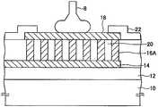
도 1은 복수 개의 본딩 패드를 갖는 반도체 소자가 일체로 구비된 집적 회로 패키지(반도체 장치)의 일부를 나타내는 사시도이다. 도 1에 나타낸 바와 같이, 반도체 장치 내에서 리드 프레임(2)의 다이 스테이지(4) 위에 탑재된 반도체 소자(6)의 본딩 패드(6a)는 본딩 와이어(8)에 의해, 리드 프레임(2)의 인너(inner) 리드(2a)에 접속되어 있다.1 is a perspective view showing a part of an integrated circuit package (semiconductor device) in which a semiconductor element having a plurality of bonding pads is integrally provided. As shown in FIG. 1, the
도 2는 도 1의 본딩 패드의 평면도이다. 또한, 도 3은 도 2에서의 Ⅲ-Ⅲ선에 따른 단면도이다.FIG. 2 is a plan view of the bonding pad of FIG. 1. 3 is sectional drawing along the III-III line | wire in FIG.
도 2 및 도 3에 나타낸 바와 같이, 일반적으로 반도체 소자 내에 형성되는 본딩 패드(6a)는 알루미늄 등으로 이루어지는 하부 배선층(14) 위에 매트릭스 모양으로 정렬된 다수의 텅스텐 등으로 이루어지는 도전성 플러그(16)를 형성하고, 그 위에 알루미늄 등으로 이루어지는 상부 도전체층(18)이 형성된 구조를 갖는다. 하부 배선층(14)과 상부 도전체층(18) 사이에서 도전성 플러그(16)의 주위에는 절연층(20)이 형성되어 있다.As shown in Figs. 2 and 3, a
또한, 하부 배선층(14)은 반도체 기판(10) 위에 형성된 층간 절연막(12) 위에 형성되어 있으며, 반도체 소자의 내부 배선이다. 또한, 상부 도전체층(18)의 외주 부분은 커버막(22)에 의해 덮이고, 커버막(22)의 개구부에서 상부 도전체층(18)이 노출되어 있다.The
상기한 구성의 본딩 패드(6a)에서, 상부 도전체층(18)의 노출된 부분에 본딩 와이어(8)가 접합된다.In the
여기에서, 반도체 소자를 형성하는 공정에 있어서, 예를 들면 전기적 시험을 행하여 반도체 소자의 양부(良否)를 판정하는 전기 특성 시험이 행하여진다. 이 경우, 반도체 소자에 전기 신호를 보내기 위해서 본딩 패드(6a)(상부 도전체층(18))에 테스트 프로브 핀을 접촉시킬 필요가 있다. 테스트 프로브 핀이 상부 도전체층(18)에 압압(押壓)되면, 상부 알루미늄층이나 도전성 플러그(16)와 비교하여 딱딱하고 부서지기 쉬운 절연층(20)에 응력이 집중한다. 이 응력에 기인하여, 도 3에 나타낸 바와 같이, 도전성 플러그(16) 사이의 절연층(20)에 균열(30)이 발생해 버리는 경우가 있다.Here, in the process of forming a semiconductor element, the electrical characteristic test which performs an electrical test, and determines the quality of a semiconductor element is performed, for example. In this case, it is necessary to bring the test probe pins into contact with the
이러한 균열은 비교적 유연한 도전성 플러그(16)까지 퍼지지 않고, 균열이 도전성 플러그(16)까지 도달한 시점에서 종결한다. 그러나, 도전성 플러그(16)는 매트릭스 모양으로 배열되어 있고, 도 4에 나타내는 단면에서는 균열이 도전성 플러그(16)와 만나지 않고, 절연층(20) 안으로 전파되는 경우가 있다.These cracks do not spread to the relatively flexible
또한, 테스트 프로브 핀을 압압함으로써 상부 도전체층(18)에 흠집이 생기고, 이 흠집이 내부의 절연층(20) 안으로 전파되는 경우가 있다. 그리고, 이 흡집 안에 수분이 침입하면, 반도체 소자 내부에 수분이 침입하여 내습성(耐濕性) 불량이 발생할 우려가 있다.Further, by pressing the test probe pins, scratches may occur in the
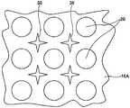
그래서, 상술한 문제를 해결하기 위해 도 5 및 도 6에 나타낸 바와 같이, 도전성 플러그와 절연층의 부분을 교체하여 격자 모양 도전부(16A)와 섬 모양의 절연층(20)으로 한 구성의 본딩 패드가 제안되어 있다(예를 들면, 특허문헌 1 참조). 또한, 도 5는 격자 모양 도전부(16A)를 갖는 본딩 패드(6Aa)의 평면도이며, 도 6은 도 5의 Ⅵ-Ⅵ선에 따른 단면도이다.Therefore, in order to solve the above-mentioned problem, as shown in Figs. 5 and 6, the bonding of the configuration in which the conductive plug and the portion of the insulating layer are replaced with the grid-shaped
즉, 상부 도전체층(18)과 하부 배선층(14) 사이에서, 도전성 플러그에 상당하는 격자 모양 도전부(16A)를 텅스텐 등으로 형성하고, 격자 모양 도전부(16A)의 내부의 각 격자에 절연재를 충전해서 절연층(20)을 형성한 구성으로 한다. 이러한 구성이면, 균열이 발생하기 쉬운 절연층(20)은 격자 모양 도전부(16A)의 벽면으로 둘러싸이게 된다. 따라서, 한개의 격자에 상당하는 절연층(20)에 균열이 발생하여도, 이 균열이 다른 격자의 절연층(20)이나, 격자 모양 도전부(16A)의 외측의 절연층(20)까지 전파하는 경우는 없다.That is, between the
[특허문헌 1] 일본국 특허 공개 2002-208610호 공보[Patent Document 1] Japanese Unexamined Patent Publication No. 2002-208610
[특허문헌 2] 일본국 특허 공개평 10-64945호 공보[Patent Document 2] Japanese Patent Application Laid-Open No. 10-64945
상술한 격자 모양 도전부(16A)는 격자 모양의 개구에 상당하는 부분(즉, 섬 모양의 절연층(20))을 형성하고, 형성된 섬 모양의 절연층(20) 사이에 텅스텐 등을 매립함으로써 형성한다. 그런데, 절연층(20)을 형성하는 절연체는 기둥 형상이며, 하부 배선층(14)과의 접촉 면적이 작기 때문에, 절연층(20)의 형성 공정에서의 에칭, 애싱, 후처리, 세정, 건조 또는 다음 공정의 세정, 건조 등의 경우에 도 7에 나타낸 바와 같이, 기둥 형상의 절연층(20)이 하부 배선층(14)으로부터 분리되어 누락되어 버리는 문제가 발생할 우려가 있다. 또한, 도 7에서 섬 모양의 절연층(20)은 사각 기둥이 아닌 원기둥으로 나타내고 있다. 도 4 및 도 5에서는 사각형 모양으로 그려져 있지만 실제로 형성하면, 원기둥에 가까운 형상이 되는 경우도 있 다.The grid-shaped
또한, 섬 모양의 절연층(20)의 주위에 텅스텐 등의 도전재를 충전할 때에, 도 8 중에서 부호 38로 나타내는 부분에 도전재가 잘 충전되지 않았거나 오목부가 생기는 등, 양호한 커버리지(coverage)를 확보할 수 없다고 하는 문제가 발생할 우려가 있다. 또한, 도 8에서도 섬 모양의 절연층(20)을 원기둥 형상으로 나타내고 있다.In addition, when the conductive material such as tungsten is filled around the island-shaped insulating
본 발명은 상술한 문제에 감안하여 이루어진 것으로서, 본딩 패드의 내부에 균열이 발생하여도, 그 균열이 반도체 소자의 내부에 전파되지 않는 구조의 반도체 소자를 제공하는 것을 목적으로 한다.This invention is made | formed in view of the above-mentioned problem, Comprising: Even if a crack generate | occur | produces inside a bonding pad, it aims at providing the semiconductor element of the structure which the crack does not propagate in a semiconductor element.
상술한 목적을 달성하기 위하여, 본 발명에 의하면 전극을 가지는 반도체 소자로서, 반도체 소자의 내부에 형성된 배선층과, 상기 배선층과 이간하여 형성되며 상기 전극의 표면을 형성하는 도전체층과, 상기 배선층과 상기 도전체층 사이에 연장되며 도전성 재료로 형성되고 서로 근접하여 배치된 복수의 주상 부재와, 상기 복수의 주상 부재 사이에 충전된 절연 재료로 이루어지는 절연층과, 상기 배선층과 상기 도전체층 사이에 연장하고, 상기 복수의 주상 부재와 상기 절연층과의 주위를 포위하도록 틀 형상으로 형성된 틀 형상 부재를 갖는 것을 특징으로 하는 반도체 소자가 제공된다.In order to achieve the above object, according to the present invention, there is provided a semiconductor device having an electrode, comprising: a wiring layer formed inside the semiconductor element, a conductor layer formed apart from the wiring layer, and forming a surface of the electrode; Extends between the conductor layers and is formed of a conductive material and is disposed adjacent to each other, an insulating layer made of an insulating material filled between the plurality of columnar members, extending between the wiring layer and the conductor layer, There is provided a semiconductor element having a frame-shaped member formed in a frame shape so as to surround the circumference between the plurality of columnar members and the insulating layer.
상술한 반도체 소자에서, 상기 틀 형상 부재는 상기 주상 부재를 형성하는 상기 도전성 재료에 의해 형성되어 있는 것이 바람직하다. 상기 틀 형상 부재는 상기 절연층을 형성하는 상기 절연 재료보다 높은 유연성을 갖는 재료로 형성되어 있는 것으로 하여도 좋다. 또한, 상기 틀 형상 부재의 외형은 상기 도전체층의 외형과 실질적으로 등동한 것이 바람직하다. 또한, 상기 주상 부재는 매트릭스 형상으로 배열되어 있는 것으로 하여도 좋다.In the above-mentioned semiconductor element, it is preferable that the said frame member is formed of the said electroconductive material which forms the said columnar member. The frame member may be made of a material having a higher flexibility than the insulating material forming the insulating layer. Moreover, it is preferable that the external shape of the said frame-shaped member is substantially equivalent to the external shape of the said conductor layer. The columnar members may be arranged in a matrix.
상술한 반도체 소자에서, 상기 배선층과 상기 도전체층 사이에 중간 도전체층이 설치되고, 상기 주상 부재는 상기 배선층과 상기 중간 도전체층 사이에 연장하는 제 1 주상 부재와, 상기 중간 도전체층과 상기 도전체층 사이에 연장하는 제 2 주상 부재를 포함하고, 상기 틀 형상 부재는 상기 배선층과 상기 중간 도전체층 사이에 연장하는 제 1 틀 형상 부재와, 상기 중간 도전체층과 상기 도전체층 사이에 연장하는 제 2 틀 형상 부재를 포함하는 것으로 하여도 좋다. 상기 제 1 및 제 2 틀 형상 부재는 상기 제 1 및 제 2 주상 부재를 형성하는 상기 도전성 재료에 의해 형성되어 있는 것이 바람직하다.In the above-described semiconductor device, an intermediate conductor layer is provided between the wiring layer and the conductor layer, and the columnar member includes a first columnar member extending between the wiring layer and the intermediate conductor layer, the intermediate conductor layer and the conductor layer. And a second columnar member extending therebetween, wherein the frame-shaped member includes a first frame-shaped member extending between the wiring layer and the intermediate conductor layer, and a second frame extending between the intermediate conductor layer and the conductor layer. A shape member may be included. It is preferable that the said 1st and 2nd frame-like member is formed of the said electroconductive material which forms the said 1st and 2nd columnar member.
또한, 본 발명에 의하면 전극을 갖는 반도체 소자의 제조 방법으로서, 반도체 소자의 내부에서의 배선층 위에, 복수의 주상 부재와 상기 복수의 주상 부재를 포위하는 틀 형상 부재를 도전성 재료에 의해 형성하고, 상기 주상 부재 사이에 절연 재료를 충전하여 절연층을 형성하며, 상기 복수의 주상 부재와 상기 절연층과 상기 틀 형상 부재의 위에 도전체층을 형성함으로써, 상기 도전체층의 표면을 상기 전극의 표면으로 하는 것을 특징으로 하는 반도체 소자의 제조 방법이 제공된다. 상기 틀 형상 부재는 상기 주상 부재와 같은 재료로 형성되는 것이 바람직하다.Moreover, according to this invention, as a manufacturing method of the semiconductor element which has an electrode, on the wiring layer inside a semiconductor element, the several columnar member and the frame-shaped member which surrounds the said several columnar member are formed with electroconductive material, Forming an insulating layer by filling an insulating material between columnar members, and forming a conductor layer on the plurality of columnar members, the insulating layer and the frame-shaped member, thereby making the surface of the conductor layer the surface of the electrode. There is provided a method of manufacturing a semiconductor device. It is preferable that the said frame member is formed of the same material as the said columnar member.
본 발명의 일 실시형태에 대하여 도면을 참조하면서 설명한다.EMBODIMENT OF THE INVENTION One Embodiment of this invention is described, referring drawings.
도 9는 본 발명의 일 실시형태에 의한 본딩 패드 부분의 평면도이다. 도 10은 도 9에서의 Ⅹ-Ⅹ선에 따른 단면도이며, 도 11은 도 9에서의 XI-XI선에 따른 단면도이다. 또한, 도 9 내지 도 11에서 도 2 및 도 3에 나타내는 부품과 동등한 부품에는 동일한 부호를 붙인다.9 is a plan view of a bonding pad portion according to an embodiment of the present invention. FIG. 10 is a cross-sectional view taken along the line VII-VII of FIG. 9, and FIG. 11 is a cross-sectional view taken along the line XI-XI of FIG. 9. In addition, in FIGS. 9-11, the same code | symbol is attached | subjected to the component equivalent to the component shown in FIG. 2 and FIG.
본 실시형태에서는 본딩 패드(40)는 2단 구조로 되어 있고, 도 10에 나타낸 바와 같이, 상하의 도전성 플러그(16)의 중간에 알루미늄 등으로 이루어지는 중간 도전체층(42)이 설치되어 있다. 본 실시형태에서는 텅스텐 등의 도전성 재료로 형성된 주상 부재인 도전성 플러그(16)에 의해 상부 도전체층(18)과 중간 도전체층(42)이 전기적으로 접속되고, 중간 도전체층(42)과 하부 배선층(14)이 전기적으로 접속되어 있다. 상부 도전체층(18)의 외부 노출면은 본딩 와이어(8)가 접합되는 본딩면으로서 기능한다.In the present embodiment, the bonding pad 40 has a two-stage structure. As shown in FIG. 10, an
이와 같이, 본 실시형태에서는 본딩 패드(40)를 2단 구조로 하고 있지만, 도 3에 나타낸 바와 같은 1단 구조여도 좋고, 3단 이상의 구조여도 좋다. 본딩 패드의 단수는 반도체 기판(10) 위에 형성된 층간 절연막(12)으로부터 상부 도전체층(18)까지의 거리에 따라 결정하면 좋다.As described above, in the present embodiment, the bonding pad 40 has a two-stage structure, but may be a single-stage structure as shown in FIG. 3 or a three-stage or more structure. The number of steps of the bonding pad may be determined according to the distance from the
본 실시형태에서는 도 9에 나타낸 바와 같이, 매트릭스 모양으로 배열된 도전성 플러그(16)의 최외주 부분이 전체 둘레에 걸쳐 연속하여 형성된 틀 형상 부재(44)로서 형성되어 있다. 본 실시형태에서는 틀 형상 부재(44)는 도전성 플러그(16)와 같은 재료, 예를 들면 텅스텐으로 형성되어 있어, 도전성 플러그(16)를 형성하는 공정에서 동시에 형성할 수 있다. 따라서, 도전성 플러그(16)와 마찬가지 로, 틀 형상 부재(44)도 하부 배선층(14)과 상부 도전체층(18)을 전기적으로 접속하는 부재로서 기능한다.In this embodiment, as shown in FIG. 9, the outermost peripheral part of the
또한, 도전성 플러그(16) 및 틀 형상 부재(44)를 형성하는 도전성 재료로서, 텅스텐(W), 구리(Cu), 알루미늄(Al) 등을 사용하는 것이 바람직하다. 또한, 절연층(20)을 형성하는 절연재로서는 산화 실리콘(SixOy), NSG, Silk, 저유전율재(Low-k) 등을 들 수 있다.In addition, it is preferable to use tungsten (W), copper (Cu), aluminum (Al), or the like as the conductive material for forming the
틀 형상 부재(44)의 폭은 1개의 도전성 플러그(16)의 폭과 같은 정도로 하는 것이 바람직하다. 예를 들면, 반도체 소자의 디자인 룰로서 0.35㎛ 룰이 적용되고 있는 경우, 틀 형상 부재(44)의 폭은 0.45㎛ 정도로 설정하는 것이 바람직하다. 또한, 0.18㎛ 룰이 적용되고 있는 경우는 0.25㎛ 정도로, 0.09㎛ 룰이 적용되고 있는 경우에는 0.15㎛ 정도로 설정한다.It is preferable that the width of the
또한, 틀 형상 부재(44)의 외형은 틀 형상 부재(44)의 내측에 다수의 도전성 플러그(16)를 배치할 수 있도록, 본딩면을 형성하는 상부 도전체층(18)의 외형과 실질적으로 동등한 것이 바람직하다.In addition, the outline of the
상술한 구성에서, 도전성 플러그(16) 및 그들 사이에 설치되는 절연 재료로 이루어지는 절연층(20)은 틀 형상 부재(44)에 의해 포위된 상태가 된다. 따라서, 도전성 플러그(16) 사이에 설치된 절연층(20)에 균열이 발생했을 경우에도, 도 11에 나타낸 바와 같이, 균열은 틀 형상 부재(44)보다 외측으로 전파하는 일이 없다. 종래의 구조를 나타내는 도 3에서, 절연층(20)에 발생한 균열(30)이 반도체 소자의 내부까지 전파하는 것에 대해, 도 11에 나타내는 본 실시형태에 의한 구조에서는 균열(30)이 틀 형상 부재(44)에 의해 멈춰 있는 것을 알 수 있다.In the above-described configuration, the insulating
이상과 같이, 본 실시형태에 의하면 테스트 프로브 핀의 접촉 시나 와이어 본딩 시에 기계적 스트레스가 본딩 패드에 가해져서, 본딩 패드 내의 절연층에 균열이 발생했다고 하여도, 균열이 반도체 소자의 내부에 전파되는 일이 없고, 균열을 따라 수분이 반도체 소자의 내부에 침입하여 내습성 불량이 발생하는 것이 방지된다. 또한, 본딩 패드 구조 내의 절연층(20)은 섬 모양이 아닌 서로 연결된 형상이 되어, 절연층(20)의 일부가 누락될 일도 없다.As described above, according to the present embodiment, even when a mechanical stress is applied to the bonding pad when the test probe pin is in contact or during wire bonding, even if a crack occurs in the insulating layer in the bonding pad, the crack propagates inside the semiconductor element. There is no work, and moisture is prevented from entering the interior of the semiconductor element along the crack and generating a moisture resistance defect. In addition, the insulating
또한, 본 실시예에 의하면 틀 형상 부재(44)에 의해 도전성 플러그(16)의 주위를 포위할 뿐만아니라, 하부 배선층(14), 중간 도전체층(42) 및 상부 도전체층(18)과 틀 형상 부재(44)에 의하여, 도전성 플러그(16) 및 그 주위의 절연층(20)을 상하 방향 및 좌우 방향으로 완전히 포위한 상태가 된다. 이에 따라, 균열이 상하 방향으로 전파하여도, 본딩 패드 구조의 외부까지 전파하는 일이 없이, 균열을 본딩 패드 구조 내(틀 형상 부재의 내측)에 봉쇄할 수 있다.In addition, according to the present embodiment, the
또한, 본 실시형태에서는 틀 형상 부재(44)를 도전성 플러그와 같은 도전성 재료로 형성하였다. 도전성 재료는 예를 들면 금속이며, 절연층(20)을 형성하는 절연 재료보다 유연한 재료이기 때문에, 균열을 멈추기 위한 재료로서 적합하며 또한 틀 형상 부재(44)를 도전성 플러그(16)와 같은 공정에서 동시에 형성할 수 있다는 이점이 있다. 그러나, 틀 형상 부재(44)는 반드시 도전성 재료로 형성할 필요는 없고, 틀 형상 부재(44)를 비교적 유연성을 갖는 절연재에 의해 형성하는 것으 로 하여도 좋다. 그러한 절연 재로서, 예를 들면 산화알루미늄(AlxOy)이나 질화 티탄 알루미늄(TixAlyNz) 등이 있다.In addition, in the present embodiment, the
상술한 본딩 패드 구조를 형성하기 위해서는, 우선 반도체 소자의 내부에서의 하부 배선층(14) 위에 복수의 도전성 플러그(16) 및 도전성 플러그(16)를 포위하도록 틀 형상 부재(44)를 하부 배선층(14) 위에 형성한 후, 도전성 플러그(16) 사이에 절연 재료를 충전하여 절연층(20)을 형성하고, 그 후 도전성 플러그(16)와 절연층(20)과 틀 형상 부재(44) 위에 상부 도전체층(18)을 형성한다. 이에 따라, 상부 도전체층(18)의 표면을 본딩 패드의 본딩면으로 할 수 있다.In order to form the above-described bonding pad structure, first, the
상술한 발명에 의하면, 테스트 프로브 핀의 접촉 시나 와이어 본딩 시나 범프 형성 시에 기계적 스트레스가 전극에 가해져서, 전극 하층의 절연층에 균열이 발생했다고 하여도, 틀 형상 부재에 의해 균열의 전파가 저지되어 균열이 반도체 소자의 내부에 전파되는 경우가 없다. 따라서, 균열을 따라 수분이 반도체 소자의 내부에 침입하여 내습성 불량이 발생하는 것이 방지된다. 또한, 전극 구조 내의 절연층은 섬 모양이 아닌 서로 연결된 형상이 되어, 제조 공정에서 절연층의 일부가 누락될 일도 없다.According to the above-described invention, even when mechanical stress is applied to the electrode at the time of contact of the test probe pin, at the time of wire bonding, or at the formation of the bump, the crack propagation is prevented by the frame member even if a crack occurs in the insulating layer under the electrode. As a result, cracks do not propagate inside the semiconductor device. Therefore, moisture is prevented from invading the inside of the semiconductor element along the cracks and the occurrence of poor moisture resistance. In addition, the insulating layers in the electrode structure are connected to each other instead of islands, so that a part of the insulating layers may not be missed in the manufacturing process.
또한, 본 발명에 의하면, 틀 형상 부재에 의해 주상 부재의 주위를 포위할 뿐만아니라, 배선층, 중간 도전체층 및 도전체층과 틀 형상 부재에 의해, 주상 부재 및 그 주위의 절연층이 상하 방향, 좌우 방향으로 완전히 포위된 상태가 된다. 이에 따라, 균열이 상하 방향으로 전파하여도 전극 구조의 외부까지 전파하는 일이 없이, 균열을 전극 구조 내에 봉쇄할 수 있다.In addition, according to the present invention, not only the frame member is surrounded by the columnar member, but also the wiring layer, the intermediate conductor layer and the conductor layer, and the frame member form the columnar member and the insulating layer around the columnar member. It is completely surrounded in the direction. Thereby, even if a crack propagates to an up-down direction, a crack can be sealed in an electrode structure, without propagating to the exterior of an electrode structure.
Claims (9)
Translated fromKoreanApplications Claiming Priority (2)
| Application Number | Priority Date | Filing Date | Title |
|---|---|---|---|
| JP2005157538AJP2006332533A (en) | 2005-05-30 | 2005-05-30 | Semiconductor device and manufacturing method thereof |
| JPJP-P-2005-00157538 | 2005-05-30 |
Publications (2)
| Publication Number | Publication Date |
|---|---|
| KR20060124532Atrue KR20060124532A (en) | 2006-12-05 |
| KR100666907B1 KR100666907B1 (en) | 2007-01-11 |
Family
ID=37462346
Family Applications (1)
| Application Number | Title | Priority Date | Filing Date |
|---|---|---|---|
| KR1020050083036AExpired - Fee RelatedKR100666907B1 (en) | 2005-05-30 | 2005-09-07 | Semiconductor device and manufacturing method thereof |
Country Status (5)
| Country | Link |
|---|---|
| US (2) | US7298051B2 (en) |
| JP (1) | JP2006332533A (en) |
| KR (1) | KR100666907B1 (en) |
| CN (1) | CN100587947C (en) |
| TW (1) | TWI278050B (en) |
Cited By (2)
| Publication number | Priority date | Publication date | Assignee | Title |
|---|---|---|---|---|
| KR101397228B1 (en)* | 2011-12-16 | 2014-05-20 | 후지쯔 가부시끼가이샤 | Semiconductor device, semiconductor device manufacturing method, and electronic device |
| KR101678162B1 (en)* | 2015-07-01 | 2016-11-21 | 서울대학교산학협력단 | Interconnection structure for flexible devices and method of manufacturing the same |
Families Citing this family (13)
| Publication number | Priority date | Publication date | Assignee | Title |
|---|---|---|---|---|
| JP2007042817A (en)* | 2005-08-02 | 2007-02-15 | Sanyo Electric Co Ltd | Insulated gate semiconductor device and manufacturing method thereof |
| JP5066836B2 (en)* | 2005-08-11 | 2012-11-07 | セイコーエプソン株式会社 | Electro-optical device and electronic apparatus |
| CN100413066C (en)* | 2005-11-30 | 2008-08-20 | 中芯国际集成电路制造(上海)有限公司 | Jointing welding plate of low-k dielectric material and method for making semiconductor device |
| US7679180B2 (en)* | 2006-11-07 | 2010-03-16 | Taiwan Semiconductor Manufacturing Co., Ltd. | Bond pad design to minimize dielectric cracking |
| US7749778B2 (en)* | 2007-01-03 | 2010-07-06 | International Business Machines Corporation | Addressable hierarchical metal wire test methodology |
| JP5034740B2 (en)* | 2007-07-23 | 2012-09-26 | ルネサスエレクトロニクス株式会社 | Semiconductor device and manufacturing method thereof |
| JP4799542B2 (en)* | 2007-12-27 | 2011-10-26 | 株式会社東芝 | Semiconductor package |
| US8178980B2 (en)* | 2008-02-05 | 2012-05-15 | Taiwan Semiconductor Manufacturing Company, Ltd. | Bond pad structure |
| JP2011146563A (en)* | 2010-01-15 | 2011-07-28 | Panasonic Corp | Semiconductor device |
| US8659170B2 (en)* | 2010-01-20 | 2014-02-25 | Taiwan Semiconductor Manufacturing Company, Ltd. | Semiconductor device having conductive pads and a method of manufacturing the same |
| US8614508B2 (en)* | 2011-09-21 | 2013-12-24 | Stats Chippac Ltd. | Integrated circuit system with test pads and method of manufacture thereof |
| JP2015103776A (en)* | 2013-11-28 | 2015-06-04 | 日本電信電話株式会社 | Pad structure for multilayer wiring |
| JP7459490B2 (en) | 2019-11-28 | 2024-04-02 | 株式会社ソシオネクスト | Semiconductor wafers and semiconductor devices |
Family Cites Families (11)
| Publication number | Priority date | Publication date | Assignee | Title |
|---|---|---|---|---|
| JPH08293523A (en)* | 1995-02-21 | 1996-11-05 | Seiko Epson Corp | Semiconductor device and manufacturing method thereof |
| JP3482779B2 (en)* | 1996-08-20 | 2004-01-06 | セイコーエプソン株式会社 | Semiconductor device and manufacturing method thereof |
| JP3149914B2 (en)* | 1997-09-11 | 2001-03-26 | 日本電気株式会社 | Method for manufacturing semiconductor device |
| US5986343A (en)* | 1998-05-04 | 1999-11-16 | Lucent Technologies Inc. | Bond pad design for integrated circuits |
| US6448650B1 (en)* | 1998-05-18 | 2002-09-10 | Texas Instruments Incorporated | Fine pitch system and method for reinforcing bond pads in semiconductor devices |
| US6552438B2 (en)* | 1998-06-24 | 2003-04-22 | Samsung Electronics Co. | Integrated circuit bonding pads including conductive layers with arrays of unaligned spaced apart insulating islands therein and methods of forming same |
| JP2001358169A (en) | 2000-06-15 | 2001-12-26 | Nec Corp | Semiconductor device |
| KR100421043B1 (en) | 2000-12-21 | 2004-03-04 | 삼성전자주식회사 | Integrated circuit bonding pads including conductive layers with arrays of unaligned spaced apart insulating islands therein |
| KR100437460B1 (en)* | 2001-12-03 | 2004-06-23 | 삼성전자주식회사 | Semiconductor device having bonding pads and fabrication method thereof |
| JP2005079288A (en)* | 2003-08-29 | 2005-03-24 | Seiko Epson Corp | Method for forming multilayer wiring and electronic device |
| JP4528035B2 (en)* | 2004-06-18 | 2010-08-18 | ルネサスエレクトロニクス株式会社 | Semiconductor device |
- 2005
- 2005-05-30JPJP2005157538Apatent/JP2006332533A/enactivePending
- 2005-08-23USUS11/208,549patent/US7298051B2/ennot_activeExpired - Lifetime
- 2005-08-23TWTW094128726Apatent/TWI278050B/ennot_activeIP Right Cessation
- 2005-09-07KRKR1020050083036Apatent/KR100666907B1/ennot_activeExpired - Fee Related
- 2005-09-09CNCN200510099898Apatent/CN100587947C/ennot_activeExpired - Fee Related
- 2007
- 2007-10-10USUS11/907,160patent/US7446029B2/ennot_activeExpired - Lifetime
Cited By (4)
| Publication number | Priority date | Publication date | Assignee | Title |
|---|---|---|---|---|
| KR101397228B1 (en)* | 2011-12-16 | 2014-05-20 | 후지쯔 가부시끼가이샤 | Semiconductor device, semiconductor device manufacturing method, and electronic device |
| US8860211B2 (en) | 2011-12-16 | 2014-10-14 | Fujitsu Limited | Semiconductor device, semiconductor device manufacturing method, and electronic device |
| KR101460938B1 (en)* | 2011-12-16 | 2014-11-12 | 후지쯔 가부시끼가이샤 | Semiconductor device, semiconductor device manufacturing method, and electronic device |
| KR101678162B1 (en)* | 2015-07-01 | 2016-11-21 | 서울대학교산학협력단 | Interconnection structure for flexible devices and method of manufacturing the same |
Also Published As
| Publication number | Publication date |
|---|---|
| US20080038914A1 (en) | 2008-02-14 |
| CN100587947C (en) | 2010-02-03 |
| TWI278050B (en) | 2007-04-01 |
| KR100666907B1 (en) | 2007-01-11 |
| US7298051B2 (en) | 2007-11-20 |
| JP2006332533A (en) | 2006-12-07 |
| TW200642017A (en) | 2006-12-01 |
| US7446029B2 (en) | 2008-11-04 |
| CN1873962A (en) | 2006-12-06 |
| US20060267222A1 (en) | 2006-11-30 |
Similar Documents
| Publication | Publication Date | Title |
|---|---|---|
| KR100329407B1 (en) | Electrode structure of semiconductor element | |
| KR100666907B1 (en) | Semiconductor device and manufacturing method thereof | |
| JP5205066B2 (en) | Semiconductor device and manufacturing method thereof | |
| JP5443827B2 (en) | Semiconductor device | |
| CN101911284B (en) | Semiconductor device and manufacturing method thereof | |
| JPH0817859A (en) | Semiconductor device | |
| CN101179057B (en) | bonding pad structure and manufacturing method thereof | |
| US20090176124A1 (en) | Bonding pad structure and semiconductor device including the bonding pad structure | |
| JP2010050177A (en) | Semiconductor device | |
| KR101349373B1 (en) | Semiconductor device and method of manufacturing a semiconductor device | |
| TWI316741B (en) | Method for forming an integrated cricuit, method for forming a bonding pad in an integrated circuit and an integrated circuit structure | |
| US6710448B2 (en) | Bonding pad structure | |
| US7429795B2 (en) | Bond pad structure | |
| JP5702844B2 (en) | Semiconductor device | |
| JP4759229B2 (en) | Semiconductor device | |
| KR20100070633A (en) | Structure for bonding pad and manufacturing method used the same | |
| CN1988144A (en) | Semiconductor device | |
| JP2015002234A (en) | Semiconductor device and method of manufacturing the same | |
| KR100971211B1 (en) | Semiconductor chip package and its manufacturing method for crack prevention | |
| WO2004093191A1 (en) | Semiconductor device | |
| JP2021150307A (en) | Semiconductor device, manufacturing method of the semiconductor device, and electronic apparatus | |
| KR20000009043A (en) | Semiconductor device having a multi-layer pad and manufacturing method thereof | |
| US20070090526A1 (en) | Semiconductor device that attains a high integration | |
| CN112951789B (en) | Lead welding structure, lead welding method and semiconductor device | |
| JP2003282574A (en) | Semiconductor device |
Legal Events
| Date | Code | Title | Description |
|---|---|---|---|
| A201 | Request for examination | ||
| PA0109 | Patent application | St.27 status event code:A-0-1-A10-A12-nap-PA0109 | |
| PA0201 | Request for examination | St.27 status event code:A-1-2-D10-D11-exm-PA0201 | |
| E701 | Decision to grant or registration of patent right | ||
| PE0701 | Decision of registration | St.27 status event code:A-1-2-D10-D22-exm-PE0701 | |
| PG1501 | Laying open of application | St.27 status event code:A-1-1-Q10-Q12-nap-PG1501 | |
| GRNT | Written decision to grant | ||
| PR0701 | Registration of establishment | St.27 status event code:A-2-4-F10-F11-exm-PR0701 | |
| PR1002 | Payment of registration fee | St.27 status event code:A-2-2-U10-U11-oth-PR1002 Fee payment year number:1 | |
| PG1601 | Publication of registration | St.27 status event code:A-4-4-Q10-Q13-nap-PG1601 | |
| PN2301 | Change of applicant | St.27 status event code:A-5-5-R10-R11-asn-PN2301 | |
| PN2301 | Change of applicant | St.27 status event code:A-5-5-R10-R14-asn-PN2301 | |
| PR1001 | Payment of annual fee | St.27 status event code:A-4-4-U10-U11-oth-PR1001 Fee payment year number:4 | |
| R18-X000 | Changes to party contact information recorded | St.27 status event code:A-5-5-R10-R18-oth-X000 | |
| PN2301 | Change of applicant | St.27 status event code:A-5-5-R10-R13-asn-PN2301 St.27 status event code:A-5-5-R10-R11-asn-PN2301 | |
| PR1001 | Payment of annual fee | St.27 status event code:A-4-4-U10-U11-oth-PR1001 Fee payment year number:5 | |
| PR1001 | Payment of annual fee | St.27 status event code:A-4-4-U10-U11-oth-PR1001 Fee payment year number:6 | |
| FPAY | Annual fee payment | Payment date:20121227 Year of fee payment:7 | |
| PR1001 | Payment of annual fee | St.27 status event code:A-4-4-U10-U11-oth-PR1001 Fee payment year number:7 | |
| FPAY | Annual fee payment | Payment date:20131218 Year of fee payment:8 | |
| PR1001 | Payment of annual fee | St.27 status event code:A-4-4-U10-U11-oth-PR1001 Fee payment year number:8 | |
| FPAY | Annual fee payment | Payment date:20141230 Year of fee payment:9 | |
| PR1001 | Payment of annual fee | St.27 status event code:A-4-4-U10-U11-oth-PR1001 Fee payment year number:9 | |
| R18-X000 | Changes to party contact information recorded | St.27 status event code:A-5-5-R10-R18-oth-X000 | |
| FPAY | Annual fee payment | Payment date:20151217 Year of fee payment:10 | |
| PR1001 | Payment of annual fee | St.27 status event code:A-4-4-U10-U11-oth-PR1001 Fee payment year number:10 | |
| FPAY | Annual fee payment | Payment date:20161220 Year of fee payment:11 | |
| PR1001 | Payment of annual fee | St.27 status event code:A-4-4-U10-U11-oth-PR1001 Fee payment year number:11 | |
| PR1001 | Payment of annual fee | St.27 status event code:A-4-4-U10-U11-oth-PR1001 Fee payment year number:12 | |
| FPAY | Annual fee payment | Payment date:20181226 Year of fee payment:13 | |
| PR1001 | Payment of annual fee | St.27 status event code:A-4-4-U10-U11-oth-PR1001 Fee payment year number:13 | |
| PR1001 | Payment of annual fee | St.27 status event code:A-4-4-U10-U11-oth-PR1001 Fee payment year number:14 | |
| PN2301 | Change of applicant | St.27 status event code:A-5-5-R10-R11-asn-PN2301 | |
| PN2301 | Change of applicant | St.27 status event code:A-5-5-R10-R14-asn-PN2301 | |
| PC1903 | Unpaid annual fee | St.27 status event code:A-4-4-U10-U13-oth-PC1903 Not in force date:20210105 Payment event data comment text:Termination Category : DEFAULT_OF_REGISTRATION_FEE | |
| PC1903 | Unpaid annual fee | St.27 status event code:N-4-6-H10-H13-oth-PC1903 Ip right cessation event data comment text:Termination Category : DEFAULT_OF_REGISTRATION_FEE Not in force date:20210105 |