KR20060120231A - Adaptive Deterministic Grouping of Blocks into Multiple Block Units - Google Patents
Adaptive Deterministic Grouping of Blocks into Multiple Block UnitsDownload PDFInfo
- Publication number
- KR20060120231A KR20060120231AKR1020067013306AKR20067013306AKR20060120231AKR 20060120231 AKR20060120231 AKR 20060120231AKR 1020067013306 AKR1020067013306 AKR 1020067013306AKR 20067013306 AKR20067013306 AKR 20067013306AKR 20060120231 AKR20060120231 AKR 20060120231A
- Authority
- KR
- South Korea
- Prior art keywords
- metablock
- block
- blocks
- memory
- linking
- Prior art date
- Legal status (The legal status is an assumption and is not a legal conclusion. Google has not performed a legal analysis and makes no representation as to the accuracy of the status listed.)
- Withdrawn
Links
Images


Classifications
- G—PHYSICS
- G06—COMPUTING OR CALCULATING; COUNTING
- G06F—ELECTRIC DIGITAL DATA PROCESSING
- G06F12/00—Accessing, addressing or allocating within memory systems or architectures
- G06F12/02—Addressing or allocation; Relocation
- G—PHYSICS
- G11—INFORMATION STORAGE
- G11C—STATIC STORES
- G11C29/00—Checking stores for correct operation ; Subsequent repair; Testing stores during standby or offline operation
- G11C29/70—Masking faults in memories by using spares or by reconfiguring
- G11C29/76—Masking faults in memories by using spares or by reconfiguring using address translation or modifications
- G—PHYSICS
- G06—COMPUTING OR CALCULATING; COUNTING
- G06F—ELECTRIC DIGITAL DATA PROCESSING
- G06F12/00—Accessing, addressing or allocating within memory systems or architectures
- G—PHYSICS
- G06—COMPUTING OR CALCULATING; COUNTING
- G06F—ELECTRIC DIGITAL DATA PROCESSING
- G06F12/00—Accessing, addressing or allocating within memory systems or architectures
- G06F12/02—Addressing or allocation; Relocation
- G06F12/0223—User address space allocation, e.g. contiguous or non contiguous base addressing
- G06F12/023—Free address space management
- G06F12/0238—Memory management in non-volatile memory, e.g. resistive RAM or ferroelectric memory
- G06F12/0246—Memory management in non-volatile memory, e.g. resistive RAM or ferroelectric memory in block erasable memory, e.g. flash memory
- G—PHYSICS
- G06—COMPUTING OR CALCULATING; COUNTING
- G06F—ELECTRIC DIGITAL DATA PROCESSING
- G06F3/00—Input arrangements for transferring data to be processed into a form capable of being handled by the computer; Output arrangements for transferring data from processing unit to output unit, e.g. interface arrangements
- G06F3/06—Digital input from, or digital output to, record carriers, e.g. RAID, emulated record carriers or networked record carriers
- G—PHYSICS
- G11—INFORMATION STORAGE
- G11C—STATIC STORES
- G11C29/00—Checking stores for correct operation ; Subsequent repair; Testing stores during standby or offline operation
- G—PHYSICS
- G11—INFORMATION STORAGE
- G11C—STATIC STORES
- G11C29/00—Checking stores for correct operation ; Subsequent repair; Testing stores during standby or offline operation
- G11C29/70—Masking faults in memories by using spares or by reconfiguring
- G11C29/78—Masking faults in memories by using spares or by reconfiguring using programmable devices
- G11C29/80—Masking faults in memories by using spares or by reconfiguring using programmable devices with improved layout
- G11C29/808—Masking faults in memories by using spares or by reconfiguring using programmable devices with improved layout using a flexible replacement scheme
- G—PHYSICS
- G06—COMPUTING OR CALCULATING; COUNTING
- G06F—ELECTRIC DIGITAL DATA PROCESSING
- G06F2212/00—Indexing scheme relating to accessing, addressing or allocation within memory systems or architectures
- G06F2212/72—Details relating to flash memory management
- G06F2212/7201—Logical to physical mapping or translation of blocks or pages
- G—PHYSICS
- G06—COMPUTING OR CALCULATING; COUNTING
- G06F—ELECTRIC DIGITAL DATA PROCESSING
- G06F2212/00—Indexing scheme relating to accessing, addressing or allocation within memory systems or architectures
- G06F2212/72—Details relating to flash memory management
- G06F2212/7208—Multiple device management, e.g. distributing data over multiple flash devices
Landscapes
- Engineering & Computer Science (AREA)
- Theoretical Computer Science (AREA)
- Physics & Mathematics (AREA)
- General Engineering & Computer Science (AREA)
- General Physics & Mathematics (AREA)
- Human Computer Interaction (AREA)
- Techniques For Improving Reliability Of Storages (AREA)
- Read Only Memory (AREA)
- For Increasing The Reliability Of Semiconductor Memories (AREA)
- Error Detection And Correction (AREA)
- Compression Or Coding Systems Of Tv Signals (AREA)
- Compression, Expansion, Code Conversion, And Decoders (AREA)
Abstract
Translated fromKoreanDescription
Translated fromKorean본 발명은 일반적으로, 반도체 비휘발성 데이터 저장 시스템들에 관한 것이며, 특히 비휘발성 데이터 저장 시스템들에서 결함들을 수용하는 더 큰 논리적 구조들로 물리적 블록들을 형성하는 시스템 및 방법에 관한 것이다.The present invention relates generally to semiconductor nonvolatile data storage systems, and more particularly to systems and methods of forming physical blocks into larger logical structures that accommodate defects in nonvolatile data storage systems.
플래시 메모리들과 같은 비휘발성 메모리 장치들은 통상 대량 데이터 저장 서브시스템들로서 사용된다. 이와 같은 비휘발성 메모리 장치들은 전형적으로, 호스트 시스템과 제거가능하게 접속되는 인클로우즈된 카드에 패키징되고, 호스트 시스템 내에서 비제거가능한 임베드된 저장장치로서 패키징될 수 있다. 전형적인 구현방식에서, 서브시스템은 하나 이상의 플래시 장치들과 종종 서브시스템 컨트롤러를 포함한다.Nonvolatile memory devices, such as flash memories, are commonly used as mass data storage subsystems. Such nonvolatile memory devices are typically packaged in an enclosed card that is removably connected to the host system and can be packaged as non-removable embedded storage within the host system. In a typical implementation, a subsystem includes one or more flash devices and often a subsystem controller.
현재 상업용 메모리 카드 포맷들은 개인용 컴퓨터 메모리 카드 국제 협회(PCMCIA)의, 컴팩트플래시(CF), 멀티미디어카드(MMC), 보안 디지털(SD), 메모리스틱, 및 메모리스틱-프로를 포함한다. 이들 카드들의 하나의 공급자는 본 출원의 양수인인 SanDisk Corporation이다. 이와 같은 카드들이 사용되는 호스트 시스템들은 디지털 카메라들, 셀룰러 전화들, 개인용 컴퓨터들, 노트북 컴퓨터들, 휴대용 컴퓨팅 장치들, 오디오 재생 장치들 등을 포함한다.Current commercial memory card formats include the Personal Computer Memory Card International Association (PCMCIA), CompactFlash (CF), Multimedia Card (MMC), Secure Digital (SD), Memory Stick, and Memory Stick-Pro. One supplier of these cards is SanDisk Corporation, the assignee of the present application. Host systems where such cards are used include digital cameras, cellular phones, personal computers, notebook computers, portable computing devices, audio playback devices, and the like.
비휘발성 메모리 장치들은 비휘발성 저장 소자들의 하나 이상의 어레이들로 이루어진다. 각 저장 소자는 하나 이상의 데이터 비트들을 저장할 수 있다. 비휘발성 메모리 어레이의 한 가지 중요한 특성은, 전력이 메모리 어레이에 더 이상 인가되지 않을 때조차도 프로그램된 데이터를 유지하는 것이다. 대조적으로, 휘발성 메모리 장치는 휘발성 메모리 어레이에 포함된 데이터를 유지하기 위해 어레이로 전력을 주기적으로 공급하여야 한다. 비휘발성 메모리의 또 다른 특성은 비휘발성 메모리 어레이 내에 포함되는 셀이 프로그램되면 이 셀은 새로운 데이터 값으로 재프로그램되기 전 소거되어야 한다는 것이다.Nonvolatile memory devices consist of one or more arrays of nonvolatile storage elements. Each storage element may store one or more data bits. One important characteristic of a nonvolatile memory array is to maintain programmed data even when power is no longer applied to the memory array. In contrast, volatile memory devices must periodically supply power to the array to maintain data contained in the volatile memory array. Another characteristic of nonvolatile memory is that once a cell contained within the nonvolatile memory array is programmed, the cell must be erased before being reprogrammed with a new data value.
메모리 셀에 전하를 저장하는 물리적 수단은 전기적으로 소거가능한 프로그램가능 판독 전용 메모리(EEPROM)와 같은 플로우팅 게이트 트랜지스터를 이용함으로써 구현될 수 있다는 것이다. EEPROMs과 같은 플로우팅 게이트 장치들이 지닌 한 가지 공지된 문제는, 매우 많은 횟수 기록, 프로그램 및 소거 사이크들 후 플로우팅 게이트가 결국 마모되어 파괴된다는 것이다. 이것이 발생될 때, 셀은 더 이상 사용될 수 없고 어레이 내의 이용가능한 메모리 셀들의 리스트를 끄집어내어야 한다. 이런 부류의 결함을 "성장된(grown)" 결함이라 칭한다. 한 가지 상업적으로 이용가능한 구현방식에서, 결함있는 셀들 밖에서 맵핑되고 새롭게 검출된 결함있는 메모리 셀들을 양호한 메모리 셀들의 물리적 어드레스들로 대체함으로써, 이들 결함들을 처리하는 것이다. 결함있는 셀들 또는 섹터들 밖에서 맵핑되고 대체 구현방식들의 예들이 1997년 8월 19일에 Mehrotra 등에게 허여된 미국 특허 5,659,550; 1997년 9월 23일에 Harari 등에게 허여된 미국 특허 5,671,229; 1999년 1월 19일에 Harari 등에게 허여된 미국 특허 5,862,080에 서술되어 있으며, 이 출원들은 본원에 전반적으로 참조되어 있다.The physical means of storing charge in a memory cell is that it can be implemented by using a floating gate transistor, such as an electrically erasable programmable read only memory (EEPROM). One known problem with floating gate devices such as EEPROMs is that after a very large number of write, program and erase cycles, the floating gate eventually wears out and breaks down. When this happens, the cell can no longer be used and must pull out a list of available memory cells in the array. This class of defects is referred to as "grown" defects. In one commercially available implementation, these defects are addressed by replacing defective memory cells mapped and newly detected outside of the defective cells with physical addresses of good memory cells. US Pat. No. 5,659,550, which maps out of defective cells or sectors and examples of alternative implementations are issued to Mehrotra et al. On August 19, 1997; U.S. Patent 5,671,229 to Harari et al. On September 23, 1997; US Patent 5,862,080 to Harari et al. On January 19, 1999, which is incorporated herein by reference in its entirety.
비휘발성 메모리 셀들의 어레이들은 전형적으로, 효율적인 수행을 위하여 판독, 프로그램, 및 소거 기능들의 그룹들로 세분화된다. 예를 들어, 많은 비휘발성 메모리 아키텍쳐들에서, 메모리 셀들은 소거 단위라 칭하는 더 큰 그룹으로 배열된다. 이 소거 단위는 한번에 소거가능한 최소수의 메모리 셀들이다.Arrays of nonvolatile memory cells are typically subdivided into groups of read, program, and erase functions for efficient performance. For example, in many nonvolatile memory architectures, memory cells are arranged in larger groups called erase units. This erase unit is the minimum number of memory cells that can be erased at one time.
소거 단위의 크기는 구현되는 메모리 아키텍쳐에 좌우된다. 초창기 비휘발성 메모리들에서, 소거 단위는 표준 512-바이트 디스크 드라이브 섹터와 동일한 크기인 블록이었다. 한 가지 상업적인 형태에서, 각 블록은 사용자 데이터의 한 섹터와 더불어 사용자 데이터 및/또는 이를 저장하는 블록과 관련된 일부 오버헤드 데이터 를 저장할 정도로 충분한 셀들을 포함한다. 셀들의 블록들이 개별적으로 소거될 수 있도록 하기 위하여, 블록들은 충분히 서로로부터 격리되어야 한다.The size of the erase unit depends on the memory architecture implemented. In early nonvolatile memories, the erase unit was a block the same size as a standard 512-byte disk drive sector. In one commercial form, each block contains enough cells to store one sector of user data and some overhead data associated with the user data and / or the block that stores it. In order for the blocks of cells to be individually erased, the blocks must be sufficiently isolated from each other.
이 격리(isolation)가 집적 회로 칩상에서 귀중한 공간을 차지하기 때문에, 이와 같은 격리를 위하여 필요로 되는 공간을 덜 차지하도록 소거 단위를 더욱 크게한 또 다른 메모리 아키텍쳐가 개발되었다. 이 대형 블록 시스템 아키텍쳐의 예는 2002년 7월 30일에 허여된 미국 특허 6,426,893의 연속 출원인 2003년 6월 17일에 Conley 등에게 허여된 미국 특허 6,580,638에 서술되어 있다. 이들 특허 둘 다는 본원에 전반적으로 참조되어 있다. 대형 블록 시스템에서, 소거 유닛은 종종 사용자 데이터를 판독하고 프로그램하는 기본 단위(프로그래밍 및/또는 판독 단위)인 개별적으로 어드레스가능한 페이지들로 더욱 세분화된다. 한 가지 상업적인 구현방식에서, 소거 단위는 메타블록이다. 메타블록은 다수의 물리적 소거 단위들로 이루어진 가상 소거 단위이다. 이들 다수의 물리적 소거 단위들은 병렬 프로그램 및 소거 동작들에 사용될 수 있지만 단일 논리적 블록으로서 어드레스된다.Because this isolation takes up valuable space on the integrated circuit chip, another memory architecture has been developed with larger erase units to take up less space needed for such isolation. An example of this large block system architecture is described in US Pat. No. 6,580,638 to Conley et al. On June 17, 2003, a serial application of US Pat. No. 6,426,893, issued July 30, 2002. Both of these patents are incorporated herein by reference in their entirety. In large block systems, the erase unit is often further subdivided into individually addressable pages, which are the basic units (programming and / or reading units) for reading and programming user data. In one commercial implementation, the erasure unit is a metablock. A metablock is a virtual erase unit made up of a plurality of physical erase units. These multiple physical erase units can be used for parallel program and erase operations but are addressed as a single logical block.
메타블록들 또는 "슈퍼" 블록들을 형성하는 한 가지 방법은 본원에 전반적으로 참조된 미국 특허 6,034,897에 서술된다. 본원에 서술된 바와 같은, 다수의 장치들을 갖는 메모리에 대해서, 각 장치들에서 동일한 물리적 블록이 메타블록 내로 그룹화된다. 이는 메타블록들 및 동일한 어드레스, 즉 장치들 중 제1 장치 내의 블록의 어드레스에 의해 어드레스될 소정 메타블록 내의 모든 블록들의 형성을 고려하지만, 이는 여러가지 제한들을 갖는다. 예를 들어, 메타블록들로 블록들의 링킹은 이 고정된 형태에서 사전 결정되기 때문에, 블록이 불량이 될 때, 메타블록 내의 다른 블록들이 여전히 기능함에도 불구하고 이 불량 블록을 포함하는 메타블록은 불량이 된다. 따라서, 바람직한 목적은 필요로 될 때마다 새로운 링킹을 설정하는 동작적인 오버헤드 없이 적응가능한 메타블록 배열을 위한 시스템 및 방법을 제공하는 것이다.One method of forming metablocks or “super” blocks is described in US Pat. No. 6,034,897, which is incorporated herein by reference in its entirety. As described herein, for a memory having multiple devices, the same physical block in each device is grouped into metablocks. This takes into account the formation of metablocks and all blocks within a given metablock to be addressed by the same address, i. For example, since the linking of blocks into metablocks is predetermined in this fixed form, when a block goes bad, the metablock containing this bad block is bad even though the other blocks in the metablock still function. Becomes Accordingly, it is a desirable object to provide a system and method for an adaptive metablock arrangement without the operational overhead of establishing a new linking whenever needed.
본 발명의 각종 양상들은 복합 논리적인 구조들로 물리적 메모리 구조들의 링킹을 위하여 종래 기술에서 발견되는 이들 및 그외 다른 제한들을 극복하는 것이다. 본 발명의 주 실시예에서, 플래시 메모리들에 메타블록 구조의 형성을 위한 기술이 제공된다. 본 발명의 제1 양상을 따르면, 메타블록으로 블록의 링킹은 메모리의 결함있는 부분들을 수용하도록 갱신된다. 결함 맵을 유지하는 시스템은 결함 맵 구조를 포함하여, 메타블록들로 조직된 비휘발성 메모리 시스템에서 공장 및 성장된 결함들(factory and grown defects)의 존재를 추적한다. 결함 맵을 유지하는 방법은 결함 맵 구조 및 메타블록의 특성들을 이용한다. 일 실시예에서, 결함 맵 구조의 크기는 비휘발성 메모리 시스템의 병렬화와 동일하다. 또 다른 실시예에서, 메타블록에 할당될 수 없는 나머지 소거 유닛들은 나중 사용을 위하여 스페어 소거 유닛들의 리스트에 유지될 것이다.Various aspects of the present invention are to overcome these and other limitations found in the prior art for linking physical memory structures into complex logical structures. In a main embodiment of the present invention, a technique for forming a metablock structure in flash memories is provided. According to a first aspect of the invention, the linking of a block into a metablock is updated to accommodate defective portions of the memory. The system maintaining the defect map tracks the presence of factory and grown defects in a nonvolatile memory system organized into metablocks, including a defect map structure. The method of maintaining the defect map uses the defect map structure and the properties of the metablock. In one embodiment, the size of the defect map structure is the same as the parallelism of the nonvolatile memory system. In another embodiment, the remaining erase units that cannot be assigned to the metablock will be kept in the list of spare erase units for later use.
본 발명의 또 다른 양상을 따르면, 메타블록들로 블록들의 링킹의 레코드는 비휘발성 메모리에 유지된다. 그 후, 컨트롤러는 필요에 따라서 자신의 휘발성 메모리로의 링킹을 판독 출력할 수 있다. 이 레코드는 결함들로부터 발생되는 재링킹들에 응답하여 갱신된다. 완전한 링킹 레코드는 예를 들어 특정 위치에서 비휘발성 메모리에 유지될 수 있거나, 단지 부분적인 링킹 레코드가 유지될 수 있다. 본 발명의 또 다른 양상에서, 메타블록들로 블록들의 초기 링킹은 예를 들어 펌웨어 기반으로 한 구현방식을 이용하는 알고리즘에 의해 결정론적으로 형성된다. 이 경우에, 비휘발성 메모리에 저장되는 링킹 레코드는 표준 알고리즘으로부터의 편차들 만을 포함할 필요가 있다.According to another aspect of the invention, a record of linking of blocks into metablocks is maintained in nonvolatile memory. The controller can then read out the linking to its volatile memory as needed. This record is updated in response to relinkings resulting from the defects. The complete linking record may be maintained in nonvolatile memory at a specific location, for example, or only a partial linking record may be maintained. In another aspect of the invention, the initial linking of blocks into metablocks is deterministically formed by an algorithm using a firmware-based implementation, for example. In this case, the linking record stored in the nonvolatile memory only needs to contain deviations from the standard algorithm.
본 발명의 부가적인 양상들, 특징들 및 장점들이 첨부 도면과 관련한 전형적인 실시예들과 관련하여 이하에서 상세히 설명된다.Additional aspects, features and advantages of the invention are described in detail below in connection with typical embodiments in conjunction with the accompanying drawings.
도 1은 비휘발성 메모리 어레이 및 메모리 컨트롤러가 호스트 시스템과 제거 가능하게 접속되는 인클로우즈된 카드에 패키징되는 기존의 비휘발성 메모리 시스템의 블록도.1 is a block diagram of an existing nonvolatile memory system packaged in an enclosed card in which a nonvolatile memory array and a memory controller are removably connected with a host system.
도2는 비휘발성 메모리 어레이가 호스트 시스템과 제거가능하게 접속된 인클로우즈된 카드에 패키징되는 기존의 비휘발성 메모리 시스템의 블록도.Figure 2 is a block diagram of an existing nonvolatile memory system in which a nonvolatile memory array is packaged in an enclosed card removably connected with a host system.
도3은 비휘발성 메모리 어레이가 호스트 시스템 내에 비-제거가능하게 임베드된 저장장치로서 임베드된 기존의 비휘발성 메모리 시스템의 블록도.Figure 3 is a block diagram of an existing nonvolatile memory system in which a nonvolatile memory array is embedded as non-removably embedded storage in a host system.
도4a는 플레인들, 존들 및 스페어들을 도시한 일 예의 칩 포맷을 도시한 도면.4A illustrates an example chip format showing planes, zones and spares.
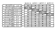
도4b-d는 메타블록들로 물리적 블록들의 각종 링킹들을 도시한 도면.4B-D illustrate various linkings of physical blocks into metablocks.
도5-10은 시스템이 메모리 어레이의 일부상에서 발생되는 일련의 성장된 결함들에 응답할 수 있는 방법을 도시한 도면.5-10 illustrate how a system can respond to a series of grown defects occurring on a portion of a memory array.
도11은 소거 유닛으로 성장된 결함의 검출에 응답하여 메타블록의 가상 구조 요소들의 맵핑의 예를 도시한 도면.FIG. 11 illustrates an example of mapping of virtual structural elements of a metablock in response to detection of a defect grown with an erase unit. FIG.
도12는 스페어 소거 유닛이 소거 유닛과 동일한 플레인에서 이용될 수 없는 결함 맵을 유지하기 위한 시스템의 예를 도시한 도면.Figure 12 shows an example of a system for maintaining a defect map in which a spare erase unit cannot be used in the same plane as the erase unit.
도13은 결함 맵을 유지하는 방법의 일 예를 도시한 도면.Figure 13 illustrates an example of a method of maintaining a defect map.
도14는 도11 내지 도13의 데이터 구조를 사용하여 결함 맵을 유지하는 방법의 예를 도시한 도면.14 illustrates an example of a method of maintaining a defect map using the data structure of FIGS. 11-13.
도15 내지 도18은 물리적 블록들의 알고리즘적으로 기반으로 한 링킹을 도시한 도면.15-18 illustrate algorithmically based linking of physical blocks.
도19, 20 및 22는 물리적 블록들의 재링킹을 도시한 도면.19, 20 and 22 illustrate relinking of physical blocks.
도21은 2차원적 경우에서 재링킹의 예를 도시한 도면.Figure 21 shows an example of relinking in the two-dimensional case.
일반적으로, 본 발명의 메모리 시스템은 다중 블록 메타블록 구조들로 블록들의 링킹의 레코드를 자신의 주 비휘발성 메모리에 유지하는 것이다. 이 레코드는 주문형 비휘발성 메모리로 판독될 수 있는 맵 테이블에서 공장 및 성장된 결함들의 결함 맵을 포함한다. 성장된 결함들에 부닥치고(encounter) 블록들이 새로운 위치들에 할당될 때 이 맵은 갱신된다. 메타블록들은 여러 서브어레이들 또는 플레인들 각각에 한 블록씩 형성되는 것이 바람직하고, 이 경우에, 그룹화는, 불량으로 표시되어 맵에 배치되는 블록들을 제외하면, 각 플레인에서 동일한 번호가매겨진 블록들로 행해지는 것이 바람직하다. 일 실시예에서, 블록들은 대체 블록들로 직접 맵핑된다. 그 후, 결함있는 블록들을 포함하는 메타블록들은 대응하는 플레인에서 대체 블록으로 재형성된다. 비휘발성 메모리 내에서 메타블록들로 블록들의 링킹의 완전한 레코드를 유지하는 것이 아니라, "표준" 링킹은 예를 들어, 시스템의 펌웨어의 알고리즘을 기반으로 할 수 있는데, 이 알고리즘으로부터의 결함들로 인한 편차들만이 저장될 필요가 있다. 현재 결함들을 갖지 않는 이들 표준 메타블록들을 사용가능한 표준 메타블록들이라 칭할 것이다. 나머지 메타블록들을 사용될 수 없는 표준 메타블록들이라 칭하고, 컴포넌트 물리적 블록들을 스페어 블록들이라 칭할 것이다.In general, the memory system of the present invention maintains a record of linking of blocks in its main non-volatile memory with multi-block metablock structures. This record contains a defect map of defects factory and grown in a map table that can be read into non-volatile memory on demand. This map is updated when grown defects are encountered and blocks are allocated to new locations. The metablocks are preferably formed one block in each of several subarrays or planes, in which case the grouping is the same numbered blocks in each plane, except for blocks that are marked as bad and placed on the map. It is preferable to carry out. In one embodiment, blocks are mapped directly to replacement blocks. Thereafter, the metablocks containing the defective blocks are reformed into replacement blocks in the corresponding plane. Rather than maintaining a complete record of the linking of blocks into metablocks in non-volatile memory, "standard" linking can be based, for example, on the algorithm of the system's firmware, due to defects from this algorithm. Only deviations need to be stored. These standard metablocks that do not currently have defects will be referred to as usable standard metablocks. The remaining metablocks will be referred to as standard metablocks that cannot be used, and the component physical blocks will be referred to as spare blocks.
도1-3은 호스트(102, 202, 302), 컨트롤러(104, 204, 304) 및 비휘발성 메모 리 어레이 또는 다수의 어레이들(103, 203, 303)을 포함하는 전형적인 기존의 비휘발성 메모리 시스템들의 블록도이다. 도1에서, 비휘발성 메모리 어레이(103) 및 메모리 컨트롤러(104)는 호스트 시스템(102)과 제거가능하게 접속되는 인클로우즈된 카드에 패키징된 것으로서 도시된다. 도2에서, 컨트롤러(204)는 호스트 시스템(202)의 부분으로서 도시되고 비휘발성 메모리 어레이(203)는 호스트 시스템과 제거가능하게 접속되는 인클로우즈된 카드에 패키징된 것으로서 도시된다. 도3에서, 비휘발성 메모리 어레이(303)는 호스트 시스템(302) 내에 비제거가능한 임베드된 저장장치로서 패키징되는 것으로서 도시된다.1-3 illustrate a typical conventional nonvolatile memory system including a
전형적으로, 비휘발성 메모리 어레이는 저장 소자들로서 하나 이상의 도전성 플로우팅 게이트들을 포함하는 메모리 셀들을 포함한다. 메모리 어레이들은 예를 들어 전하 트랩핑 유전체 대신에 다른 장기간 전자 전하 저장 소자들을 포함할 수 있다. 비휘발성 다중-상태 저장 소자들, Flash/EEPROM/플로우팅 게이트인 저장 소자들, NROM, MNOS, MRAM/FRAM, NAND, NOR와 같은 비휘발성 저장 소자들 및 소거 유닛들로 조직되는 비휘발성 저장 소자들을 포함한 각종 비휘발성 저장 소자들이 사용될 수 있다. 디지털 정보, 아날로그 정보 또는 이들 둘 다의 조합을 저장하는 비휘발성 저장 소자들이 사용될 수 있다.Typically, a nonvolatile memory array includes memory cells that include one or more conductive floating gates as storage elements. Memory arrays may include other long term electronic charge storage elements instead of, for example, a charge trapping dielectric. Nonvolatile multi-state storage devices, storage devices that are Flash / EEPROM / floating gates, nonvolatile storage devices such as NROM, MNOS, MRAM / FRAM, NAND, NOR and nonvolatile storage devices organized into erase units Various nonvolatile storage elements can be used, including. Nonvolatile storage elements may be used that store digital information, analog information, or a combination of both.
메모리 셀 어레이는 각 저장 소자를 위하여 규정된 2개의 전하 레벨들로 동작되어 각 소자에 하나의 데이터 비트를 저장한다. 대안적으로, 2가지 이상의 저장 상태들은 각 저장 소자를 위하여 규정될 수 있는데, 이 경우에 하나 이상의 데이터 비트는 각 저장 소자에 저장된다.The memory cell array is operated at two charge levels defined for each storage element to store one data bit in each element. Alternatively, two or more storage states can be defined for each storage element, in which case one or more data bits are stored in each storage element.
도4a는 메모리 칩이 소거 유닛들(또는 블록들)의 그룹들로 포맷화될 수 있는데, 이 블록들은 물리적 플레인들 및 논리적 존들에 따라서 배열된다. 이 방식에서 칩을 분할하는 몇 가지 이유들은, 각 그룹내에서 양호한 소거 유닛들의 수를 동일하게 하고 메모리 칩의 특수용 섹션들을 제외하는 것을 포함한다. 예를 들어, 특수한 "예약된" 섹션은 시스템 및 장치 파라미터들과 같은 정보 및 존 얼라인먼트(zone alignment)에 관한 정보를 저장하기 위하여 제외될 수 있다. 섹션은 또한 스페어들 또는 스페어 블록들로서 공지된 스페어 소거 유닛들을 저장하기 위하여 제외될 수 있다. 스페어들, 예를 들어, 스페어들의 물리적 어드레스들과 관련되는 정보는 필요한 경우 검색을 위하여 스페어 리스트에 유지될 수 있다. 예를 들어, 결함이 N개의 존들 중 한 존에 포함된 소거 유닛들 중 한 유닛에서 검출될 때, 스페어는 결함있는 소거 유닛을 이용가능한 스페어 소거 유닛들 중 한 유닛에 재맵핑함으로써 발견될 수 있다.4A shows that a memory chip may be formatted into groups of erase units (or blocks), which are arranged in accordance with physical planes and logical zones. Some reasons for dividing the chip in this manner include equalizing the number of good erase units in each group and excluding special sections of the memory chip. For example, a special "reserved" section may be excluded to store information such as system and device parameters and information about zone alignment. The section may also be excluded to store spare erase units known as spares or spare blocks. Spares, for example information related to the physical addresses of the spares, may be maintained in the spare list for retrieval if necessary. For example, when a defect is detected in one of the erase units included in one of the N zones, the spare can be found by remapping the defective erase unit to one of the available spare erase units. .
호스트로부터의 데이터는 전형적으로, 논리적 섹터들로서 식별되는 메모리 시스템에만 제공된다. 예를 들어, 호스트는 시작 논리적 섹터 및 총 섹터수와 관련하여 나타낸 데이터를 전송할 것이다. 호스트 내에서, 이들 논리적 섹터들은 더 큰 유닛들로 구조화될 수 있지만, 이 정보는 전형적으로 메모리의 컨트롤러로 통과되지 않는다. (이들 호스트 구조들에 대한 지식은 메모리 또는 컨트롤러 구성들에서 물리적 구조들을 알도록 하는데 사용되지만, 이들 구성들은 호스트가 데이터를 전송하는 방법을 반영하기 때문에 이들 호스트 구조들을 반영한다: 예를 들어, 메모리들은 전형적으로 논리적 섹터와 동일한 크기인 물리적 섹터를 토대로 사용자 데 이터를 저장하도록 구조화된다). 컨트롤러는 논리적 구성들로 호스트 구조들을 조직하는데, 이 논리적 구성들은 물리적 메모리에 이들을 더욱 효율적으로 저장하기 위한 물리적 구조를 모방한다. 예를 들어, 통상적인 배열에서, 메모리 시스템 컨트롤러는 논리적 섹터들(호스트에 의해 규정됨)을 블록의 물리적 구조에 크기면에서 대응하는 논리적 블록들로 그룹화하는데, 이는 플래시 형 메모리용 물리적 소거 유닛이다. 그 후, 컨트롤러는 예를 들어 섹터 어드레스 테이블(SAT)의 형태로 논리적 구성들에 대한 물리적 구조의 관계를 유지시키고 논리적 대 물리적 관계 변화들에 따라서 이 대응성을 갱신한다.Data from the host is typically provided only to a memory system identified as logical sectors. For example, the host will send the indicated data in relation to the starting logical sector and the total number of sectors. Within the host, these logical sectors can be structured into larger units, but this information is typically not passed to the controller of the memory. (Knowledge of these host structures is used to know the physical structures in memory or controller configurations, but these configurations reflect these host structures because they reflect how the host transmits data: for example, memory. Are typically structured to store user data based on physical sectors that are the same size as the logical sectors). The controller organizes the host structures into logical configurations, which mimic the physical structures for storing them more efficiently in physical memory. For example, in a typical arrangement, the memory system controller groups logical sectors (defined by the host) into logical blocks that correspond in size to the physical structure of the block, which is a physical erase unit for flash type memory. . The controller then maintains the relationship of the physical structure to the logical configurations, for example in the form of a sector address table (SAT), and updates this correspondence in accordance with logical to physical relationship changes.
더 큰 효율을 위하여, 메모리 시스템들은 종종 더 큰 구조들을 도입함으로써 병렬화를 개선시킨다. 예를 들어, 기록, 판독 또는 이들 둘 다를 동시에 할 수 있는 다수의 반자동 어레이들을 갖는 메모리 시스템에서, 여러 어레이들로부터 블록들은 "메타블록" 구조들로 그룹화되고 컨트롤러는 데이터의 논리적 블록들을 대응하는 논리적 메타블록들로 형성하여, 다수의 블록들이 동시에 동작되도록 한다. 메타블록은 단일 메모리 칩을 갖는 플레인들 또는 여러 메모리 칩들에 걸쳐서 분포되는 하나 이상의 플레인들로부터 형성될 수 있다. 이 방식으로, (논리적으로) 순차적인 섹터들이 병렬로 판독/프로그램/소거될 수 있는 다수의 물리적 블록들에 걸쳐있도록 함으로써, 이 그룹은 최소수의 비동시 판독, 프로그램, 또는 소거 동작들과 동시에 판독/프로그램/소거될 수 있다. 이 배열은 상대적으로 많은 량의 데이터의 논리적으로 연속한 섹터들을 순차적으로 판독 및 기록하는데 유용하다.For greater efficiency, memory systems often improve parallelism by introducing larger structures. For example, in a memory system with multiple semi-automatic arrays capable of writing, reading, or both at the same time, blocks from multiple arrays are grouped into "metablock" structures and the controller is a logical grouping of the corresponding logical blocks of data. Formed with metablocks, multiple blocks can be operated simultaneously. The metablock may be formed from planes with a single memory chip or one or more planes distributed across several memory chips. In this way, by allowing (logically) sequential sectors to span multiple physical blocks that can be read / programmed / erased in parallel, this group is concurrent with the minimum number of asynchronous read, program, or erase operations. Can be read / programmed / erased. This arrangement is useful for sequentially reading and writing logically contiguous sectors of a relatively large amount of data.
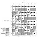
도5 내지 도10의 구조가 우선 논의되고 나서 각 도면에 도시된 동작들이 개 별적으로 설명될 것이다. 도5-10은 도1-3의 메모리 어레이의 예로서 총 24개의 소거 유닛들에 대해서 4개의 플레인들에서 6개의 블록들의 배열을 도시한다. 간편성을 위하여, 소거 유닛들은 블록이 일종의 소거 유닛이기 때문에 블록이라 칭할 것이다. 이 6×4 블록 구조의 크기는 후술되는 바와 같이 설명을 간편하게 하기 위하여 선택된다. 전형적인 메모리 어레이는 본원에 도시된 것보다 훨씬 많은 블록들을 포함하고(훨씬 많은 로우들을 갖는다) 비휘발성 메모리 시스템의 병렬화가 4개보다 큰 경우 도시된 것보다 더 많은 플레인들을 가질 수 있다.The structure of Figs. 5 to 10 will be discussed first and then the operations shown in each figure will be described separately. 5-10 show an arrangement of six blocks in four planes for a total of 24 erase units as an example of the memory array of FIGS. 1-3. For simplicity, erase units will be called blocks because the block is a type of erase unit. The size of this 6x4 block structure is chosen for simplicity of explanation as will be described later. A typical memory array may contain much more blocks (have much more rows) than shown here and may have more planes than shown when the parallelism of a nonvolatile memory system is greater than four.
각 플레인은 전형적으로, 자체 데이터 레지스터들 및 프로그래밍 회로들을 갖는다. 이는 플레인들 각각의 메모리 셀들의 블록들로 동시 프로그램을 허용한다. 각 플레인은 다른 플레인들과 반독립적으로 동작될 수 있다. 도시를 간단히 하기 위하여, 도5-10에 도시된 플레인들은 6개의 물리적 블록들(0-5)을 갖도록 도시된다. 임의의 소정 형태에서 실제 블록들의 수는 더 작을 수 있지만, 통상적으로 훨씬 더 많다.Each plane typically has its own data registers and programming circuits. This allows simultaneous programming with blocks of memory cells in each of the planes. Each plane can operate semi-independently from the other planes. For simplicity of illustration, the planes shown in FIGS. 5-10 are shown having six physical blocks 0-5. In any given form the number of actual blocks may be smaller, but typically much more.
많은 수의 블록들이 존재하는 시스템에서, 플레인들은 도4a에 도시된 바와 같이 존들로 논리적으로 분할될 수 있다. 이 존들은 다수의 플레인들에 걸쳐서 확장된다. 플레인을 더욱 소형의 더 많은 관리가능한 세그먼트들로 분할하기 위해선 플레인들을 존들로의 분할이 행해진다. 존 내의 각 플레인에서 블록들은 동일한 연속적인 세트의 물리적 블록 어드레스들을 차지할 수 있다. 존들의 수는 특히 제한되지 않지만, 실제 설계 판정들은 특정 메모리 시스템에서 구현되는 존들의 수에 영향을 미칠 수 있다. 본 발명의 각종 양상들은 존 구조를 갖거나 갖지 않는 메모 리에서 구현될 수 있고, 존 구조를 갖는 메모리들에 대해선 전체적으로 또는 개별적인 존들을 갖는 플레인들 내에서 구현될 수 있다.In a system with a large number of blocks, the planes can be logically divided into zones as shown in FIG. 4A. These zones extend across multiple planes. To divide the plane into smaller, more manageable segments, the plane is divided into zones. Blocks in each plane in the zone may occupy the same contiguous set of physical block addresses. The number of zones is not particularly limited, but actual design decisions may affect the number of zones implemented in a particular memory system. Various aspects of the present invention may be implemented in memory with or without a zone structure, and may be implemented in planes having entirely or separate zones for memories having a zone structure.
도5-10에서 시나리오들에 적용되는 바와 같은 메모리 시스템에 의해 사용되는 동작 유닛은 바람직하게는 메타블록이다. 메타블록은 플레인들에 걸쳐서 다수의 물리적 블록들의 가상 링킹을 나타낸다. 메타블록의 선택적인 이용들은 메타블록 내의 모든 블록들의 파이프라인 소거, 및 메타블록의 각 블록으로부터 하나 이상의 페이지들의 파이프라인 프로그래밍 및 판독을 포함한다.The operating unit used by the memory system as applied to the scenarios in Figures 5-10 is preferably a metablock. Metablocks represent virtual linking of multiple physical blocks across planes. Optional uses of the metablock include pipeline erasure of all blocks within the metablock, and pipeline programming and reading of one or more pages from each block of the metablock.
메타블록은 다수의 플레인들에 걸쳐서 확장되고 전형적으로 도5-10에 도시된 연결된 화살표들의 세트들 각각에서 화살표들로 도시된 바와 같은 이들 플레인들 각각으로부터 하나의 블록을 포함한다. 도5는 가장 간단한 형태의 메타블록을 도시하는데, 모든 메타블록의 각 물리적 블록은 동일한 블록 오프셋을 갖고 모두 4개의 플레인들(0-3)에 걸쳐서 확장된다. 도10은 2개 이상의 복잡한 메타블록들을 도시한다. 이들 메타블록들의 생성은 도5-10의 설명에서 논의되는데, 메타블록에 포함되는 컴포넌트 블록들은 결함들에 부닥칠 때 갱신된다.The metablock extends over multiple planes and typically includes one block from each of these planes as shown by the arrows in each of the connected sets of arrows shown in FIGS. 5-10. Figure 5 shows the simplest form of metablock, where each physical block of all metablocks has the same block offset and extends across all four planes 0-3. 10 shows two or more complex metablocks. The generation of these metablocks is discussed in the description of FIGS. 5-10, wherein the component blocks included in the metablock are updated when encountering defects.
블록들을 메타블록들로 링킹하기 위한 더욱 일반적인 상황이 도4b에 도시된다. 시스템의 메모리 부분(도1-3 각각의 103, 203, 303)은 칩(0-Z)으로 이루어지며, 각 칩은 칩(0)DP 대해서 플레인들(00 내지 0W)과 같은 다수의 플레인들을 갖는다. x로 표시된 플레인에서 각 링크된 물리적 유닛은 도4c에 도시된 바와 같이 단일 물리적 블록 또는 도4d에 도시된 바와 같이 다수의 물리적 블록들로 이루어질 수 있다. 플레인들 및 칩들에 걸쳐서뿐만 아니라 깊이에서 블록들을 링크하는 도4d 에 도시된 2차원 메타블록들의 정렬은 특히 물리적 블록들이 작을 때 간편하게 될 수 있다. 그러나, 간편성이 도4d의 배열에 대한 주 이유일 수는 없다. 통상적으로 1차원 링킹의 주요 동기는 상이한 칩들/플레인에서 다수의 블록들에 기록될 수 있는 데이터를 동시에 취급하기 위한 메커니즘을 제공하는 것이다. 유사하게, 메모리 디자인이 병렬의 플레인 내의 하나 이상의 위치에 병렬 액세스(판독 및 프로그램)을 허용하면, 이는 동일한 플레인 내에서 다수의 블록들을 링크하는 것을 의미할 수 있다.A more general situation for linking blocks into metablocks is shown in FIG. 4B. The memory portion of the system (103, 203 and 303 in Figures 1-3 respectively) consists of chips (0-Z), each chip having a number of planes such as planes (00 to 0W) for chip (0) DP. Have Each linked physical unit in the plane labeled x may consist of a single physical block as shown in FIG. 4C or multiple physical blocks as shown in FIG. 4D. The alignment of the two-dimensional metablocks shown in FIG. 4D linking blocks in depth as well as across planes and chips can be simplified, especially when the physical blocks are small. However, simplicity may not be the main reason for the arrangement of FIG. 4D. Typically the main motivation for one-dimensional linking is to provide a mechanism for simultaneously handling data that can be written to multiple blocks on different chips / planes. Similarly, if the memory design allows parallel access (read and program) to one or more locations in the parallel plane, this may mean linking multiple blocks within the same plane.
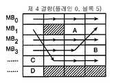
여러 메타블록 링킹들이 도시되어 있으며, 각 메타블록(MB)은 링킹에서 제1 블록의 제1 로우에 따라서 번호가 매겨지는데, 예를 들어, 블록 0으로 시작하는 메타블록은 MB0로 라벨링, 등등으로 된다. 도4b가 소정 링킹에서 그리고 여러 플레인들에 걸쳐서실행되는 링킹에서 블록(및 단지 하나의 블록)을 갖는 각 플레인을 도시하지만, 이 상황들중 어느 것도 항상 이 경우가 될 필요가 있다. 예를 들어, 도5-10에서와 같이 4개의 블록들의 링킹은 단일 칩상에서 4개의 플레인들 또는 4개의 플레인들로부터 하나의 플레인으로 이루어질 수 있다.Several metablock linkings are shown, where each metablock MB is numbered according to the first row of the first block in the linking, for example, a metablock beginning with block0 is labeled MB0 , etc. Becomes Figure 4b is in some linking and across several planes While each plane has a block (and only one block) in the linking executed, none of these situations always need to be the case. For example, as shown in Figs. 5-10, the linking of four blocks may be made of one plane from four planes or four planes on a single chip.
도4b에 도시된 바와 같이, 링킹(MBO)은 동일한 로우로부터의 모든 블록들을 가지며, MB1은 동일한 로우로부터의 대부분의 블록들을 갖고, MB2는 선행 블록보다 적은 로우로부터의 각 블록을 갖는다. 도5-10에 설명은, 이 설명을 간편하게 하기 위하여 동일한 로우로부터의 모든 블록들을 갖는 MB0경우를 취하는데, 더욱 일반적 인 경우가 후술된다. 이들 각종 링킹 방법들은 고정되거나, 이하에 더욱 상세하게 설명되는 본 발명의 양상을 따르면, 알고리즘을 토대로 결정된다. (대안적으로, 초기 결정은 랜덤 할당을 토대로 할 수 있다). 더욱 일반적인 내용에서, 본 발명의 각종 양상들은 일반적으로 물리적 구조들이 더 큰 논리적 컨글로메이트들(logical conglomerates)로 형성되고 이들 컨글로메이트들이 관리되는 방법에 적용될 수 있다.As shown in FIG. 4B, linking MBO has all the blocks from the same row, MB1 has most of the blocks from the same row, and MB2 has each block from fewer rows than the preceding block. . The description in Figures 5-10 shows MB0 with all blocks from the same row to simplify this description. Take the case, a more general case is described below. These various linking methods are fixed or determined based on an algorithm, according to aspects of the present invention described in more detail below. (Alternatively, the initial decision may be based on random allocation). In a more general context, various aspects of the present invention are generally applicable to the way in which physical structures are formed of larger logical conglomerates and how these conglomates are managed.
도10에 도시된 바와 같은 제1 메타블록은 4개의 플레인들(0-3) 각각에서 블록(0)을 포함하고, 제2 메타블록은 플레인(0)에서 블록(1),플레인(1)에서 블록(4), 플레인(3)에서 블록(5) 및 플레인(3)에서 블록(4)를 포함한다. 제3 메타블록은 4개의 플레인들(0-3) 각각에서 블록(2)을 포함한다. 제4 메타블록은 플레인(0)에서 블록(3), 플레인(1)에서 블록(3), 플레인(2)에서 블록(3), 및 플레인(3)에서 블록(1)을 포함한다.The first metablock as shown in FIG. 10 includes
대안적으로, 메타블록은 단일 존 내에 포함되는 플레인들의 수의 서브셋 만을 포함한다. 이 예는 도시되지 않았지만 가변 병렬화 정도가 바람직한 경우 유용하게 될 수 있다. 가변 병렬화 정도를 갖는 시스템은 블록들을 상이한 병렬화를 갖는 에어리어들 간에서 이동시킬 수 있다. 예를 들어, 4개 대신에 2개의 블록들을 포함하는 메타블록은 병렬화가 2(2개의 플레인들)인 에어리어에서부터 (예를 들어 4-플레인에서처럼) 병렬화가 4인 에어리어로 이동할 수 있다. 2개의 멤버들을 각각 포함하는 2개의 메타블록들이 이와 같은 시스템에 존재하면, 이들은 하나의 4-멤버 메타블록에 결합될 수 있다. 이와 같은 혼합된 병렬화 시스템을 이용하기 위한 한 가지 방법은, 결함 맵이 가변하는 병렬화를 고려하도록 조정되어야 한다는 것이다.Alternatively, the metablock contains only a subset of the number of planes contained within a single zone. This example is not shown but may be useful if variable degree of parallelism is desired. Systems with varying degrees of parallelism can move blocks between areas with different parallelisms. For example, a metablock containing two blocks instead of four may move from an area with parallelism of two (two planes) to an area with four parallelisms (as in, for example, four planes). If two metablocks, each containing two members, exist in such a system, they can be combined into one 4-member metablock. One way to use such a mixed parallelization system is that the defect map must be adjusted to account for varying parallelism.
일반적으로, 메타블록들을 이용하면, 더 많은 블록들이 병렬로 한번에 처리되도록 함으로써 메모리 시스템의 병렬화를 증가시킨다. 이 증가된 병렬화는 메모리 시스템의 수행성능을 크게 증가시킨다. 메모리 시스템은 각종 메타블록들 내에서 개별적인 블록들의 아이덴터티를 유지한다. 예를 들어, 각종 메타블록들 내의 개별적인 블록들의 아이덴터티는 시스템 내의 어떤 간편한 위치에서 링크된 리스트로서 유지될 수 있다.In general, using metablocks increases the parallelism of the memory system by allowing more blocks to be processed in parallel at one time. This increased parallelism greatly increases the performance of the memory system. The memory system maintains the identity of individual blocks within various metablocks. For example, the identity of individual blocks in various metablocks may be maintained as a linked list at any convenient location in the system.
통상적으로, 각 페이지의 사용자 데이터와 함께 저장된 오버헤드 데이터는 플레인, 존 및 페이지들이 상주하는 블록을 식별하는데 충분한 논리적 및/또는 물리적 어드레스뿐만 아니라 이 블록 내 페이지의 오프셋을 포함할 것이다. 그 후, 어드레스 맵은 페이지 오버헤드 데이터의 이들 어드레스 필드들을 판독하는 컨트롤러에 의해 컨트롤러의 메모리 내에서 생성된다. 이는 통상적으로, 이 메모리의 파트에 관한 프로그래밍, 판독 또는 소거 동작에 앞서 한번에 메모리의 파트에 대해서 행해진다.Typically, the overhead data stored with the user data of each page will include an offset of the page within this block as well as a logical and / or physical address sufficient to identify the block in which the plane, zone and page reside. The address map is then generated in the controller's memory by the controller reading these address fields of page overhead data. This is typically done for parts of the memory at one time prior to programming, reading or erasing operations on those parts of the memory.
도5-10은 시스템이 메모리 어레이의 물리적 블록들에서 결함들의 검출에 응답하는 방법을 도시한 것이다. 이들 결함들은 공장 또는 성장된 결함들일 수 있다. 이 일련의 도면들은, 새로운 결함에 부닥칠 때마다 발생되는 것을 나타내고자 하는 것이다. 도시를 위하여, (1-5)로 번호가 매겨진 물리적 블록들은 결함들을 포함한다.5-10 illustrate how the system responds to detection of defects in physical blocks of a memory array. These defects can be factory or grown defects. This series of drawings is intended to show what happens whenever a new defect is encountered. For illustration purposes, the physical blocks numbered 1-5 contain defects.
제1 도면, 즉 도5는 결함들이 없는 메모리 어레이의 일부분을 도시한 것이 다. 다수의 메타블록들은 모두 4개의 플레인들을 가로질러 진행하는 6개의 수평 화살표들로 도시된다. 각 메타블록은 규정된 수의 물리적 블록들을 포함한다. 도5-10에서, 규정된 수의 물리적 블록들은 모든 메타블록들에 대해서 4개인데, 이는 플레인들의 수에 대응한다.5 shows a portion of a memory array without defects. Multiple metablocks are shown with six horizontal arrows running across all four planes. Each metablock contains a prescribed number of physical blocks. In Figures 5-10, the prescribed number of physical blocks is four for all metablocks, which corresponds to the number of planes.
도5는 공장 또는 성장된 결함들이 발견되지 않는 메모리 어레이의 일부분을 도시한 것이다. 이 도면을 가로질러 수평으로 진행하는 블랙 화살표들은 6개의 선형 표준 메타블록들을 도시한다. 선형 표준 메타블록은 도5에 도시된 바와 같은 정합하는 오프셋들을 갖는 물리적 블록들을 포함하는 메타블록이다. 초기 링킹들은 후술되는 바와 같이 알고리즘에 따라서 설정되거나 이용가능한 양호한 블록들의 소거 풀(pool)로부터 형성될 수 있다.Figure 5 illustrates a portion of a memory array in which no factory or grown defects are found. The black arrows running horizontally across this figure show six linear standard metablocks. The linear standard metablock is a metablock that includes physical blocks with matching offsets as shown in FIG. Initial linkings may be formed from an erase pool of good blocks that are set or available according to an algorithm as described below.
본 발명의 일 실시예에서, 메타블록의 특징은, (제1 물리적 블록 어드레스와 관련되는) 제1 가상 블록 어드레스가 특정 메타블록과 관련된 나머지 물리적 블록들의 위치들을 결정하는데 필요로 되는 유일한 정보라는 것인데, 링킹된 메타블록들의 나머지는 링킹 알고리즘에 의해 결정된다. 이는 메타블록들을 저장하는데 필요로 되는 데이터의 크기를 감소시킨다. 결함이 제1 물리적 블록에서 부닥치면, 전체 메타블록은 무효하게 되고 이용가능한 플레인들 또는 플레인들 각각에 걸쳐서 위치되는 메타블록의 나머지 멤버들을 가리키는 어떠한 메커니즘이 더이상 존재하지 않기 때문에 어드레스 공간 밖에서 맵핑된다. 이의 예는 이하의 도9의 논의에서 도시될 것이다.In one embodiment of the invention, a feature of the metablock is that the first virtual block address (associated with the first physical block address) is the only information needed to determine the locations of the remaining physical blocks associated with the particular metablock. The remainder of the linked metablocks is determined by a linking algorithm. This reduces the size of data needed to store the metablocks. If a defect is encountered in the first physical block, the entire metablock is invalidated and mapped out of the address space because there is no longer any mechanism pointing to the available planes or remaining members of the metablock located across each of the planes. An example of this will be shown in the discussion of FIG. 9 below.
도6은 제1 새로운 결함이 부닥친 후 어레이의 상태를 도시한 것이다. 새로운 결함이 플레인(2) 상의 블록(1)에 위치되는 "A"로 라벨된 물리적 블록의 MB1에 위치된다. 메타블록 내의 물리적 블록이 불량일 때, 메타블록은 그 대로 더이상 사용될 수 없다. 한 가지 간단한 해결책은, 어드레스 공간 밖에서 메타블록을 맵핑하고 이를 다시 결코 사용하지 않는 것이다. 이는 시스템이 단지 하나의 단일 불량 물리적 블록만을 갖고 스페어 블록들이 이용될 수 없는 경우에 이용할 수 있는 유일한 해결책이다. 그러나, 다수의 불량 물리적 블록들이 나타나는 경우, 이 해결책은 불량 메타블록과 관련된 나머지 물리적 블록들이 다른 양호한 메타블록들을 생성하는데 사용될 수 있기 때문에 빠르게 무용하게 된다. 도6에서 발견된 결함("A"로 라벨됨)에 따라서, 나머지 3개의 양호한 물리적 블록들(해치 마크로 도시)은 스페어들이 된다.Figure 6 shows the state of the array after a first new defect is encountered. The new defect is located in MB1 of the physical block labeled "A" which is located in
도7은 제2의 새로운 결함에 부닥친 후 어레이의 상태를 도시한 것이다. 새로운 결함은 플레인(3) 상의 블록(3)에서 MB2에 위치되는 "B"로 라벨된 물리적 블록에 있다. 도11에 도시된 맵과 같은 결함 맵을 유지하기 위한 방법에서, 결함이 발생된플레인(플레인 3)이 임의의 이용가능한 스페어 블록들에 대해서 탐색될 것이다. 여기서, 물리적 블록(1)(도6에서 해치로 도시되어 있다)은 플레인(3)에서 이용될 수 있다. 블록(1)이 플레인(3)에서 이용될 수 있기 때문에, 메타블록은 블록(1)을 가리키도록 갱신되어 메타블록의 결함있는 부분을 대체한다. 즉, 플레인(3)에서 MB3 의 결함있는 블록은 MB1의 플레인(2)에서 블록 "A"의 불량으로 인해 여분인 MB1의 플레인(3)에서 양호한 블록으로 링킹에서 대체된다. 불량한 물리적 블록에 부닥칠 때, 스페어 물리적 블록은 메타블록에 링킹되어, 불량 물리적 블록의 위치를 취한다.Figure 7 shows the state of the array after encountering a second new defect. The new defect is in a physical block labeled "B" located at MB2 in
(사용된 명칭 협약하에서, 도6 및 도7의 지점에서 메타블록(MB1)이 존재하지 않는데, 그 이유는 전체 메타블록이 플레인(0)에서 블록 번호를 토대로 명명되기 때문이다. 명명된 MB1은 플레인(0)에서 블록(1)이 도8에서 발생되는 바와 같이 새로운 링킹에서 리턴되지 않는 한 철회(retire)된다).(Under the naming convention used, there is no metablock MB1 at the points in Figs. 6 and 7 because the entire metablock is named based on the block number in
도8은 제3의 새로운 결함에 부닥친 후 어레이의 상태를 도시한 것이다. 새로운 결함은 플레인(0) 상의 블록(4)에 위치되는 "C"로 라벨된 물리적 블록에 위치된다. 이 메타블록은 결함있는 블록이 플레인(0) 상에 위치되기 때문에 재링킹된다. 플레인(0) 상에 위치되는 블록은 메타블록의 멤버들의 나머지에 대한 참조 정보를 포함하고 플레인(0) 상에 블록이 없다면, 채택된 협약하에서 메타블록을 참조할 방법은 없다. 그러므로, 스페어 블록이 플레인(0) 상의 블록(1)에서 이용될 수 있을 지라도, 이는 이 메타블록을 완성하기 위하여 사용될 수 없다. 대신에, 플레인(0) 상의 블록(1)은 가상 어드레스 공간으로 재맵핑되고 새로운 메타블록에서 제1 블록으로서 사용되어 이전 메타블록(MB4)의 플레인들(1, 2 및 3)에서 새로운 용장 블록들을 이용한다. 따라서, 결함있는 블록 "A"은 플레인(2)의 블록(4)로 대체될 수 있다. 플레인(3)의 블록(1)이 도7에서 재맵핑될 때, 이는 또한 대체될 필요가 있다. 결국, 재링크된(MB1)은 플레인들(2 및 3)로부터 블록(4)에서 스페어들을 이용하여 형성될 수 있다. 플레인(1)에 대해서, 블록은 블록(1) 및 블록(4)에서 이용될 수 있다. 이 블록중 어느 한 블록이 재링크된 MB1을 완성하기 위하여 선택될 수 있을 지라도, MB4에서 이전 블록이 이 예에서 사용된다. 결국, 재링크된 MB1은 플레인(0) 상의 블록(1), 플레인(1) 상의 블록(4), 플레인(2) 상의 블록(4), 및 플레인(3) 블록(4)를 포함한다. 이 때에, 단지 하나의 스페어 블록이 플레인(1) 상의 블록(1)에 남아있다.8 shows the state of the array after encountering a third new defect. The new defect is located in a physical block labeled "C" which is located in
도9는 제4의 새로운 결함에 부닥친 후 어레이의 상태를 도시한 것이다. 새로운 결함은 플레인(0) 상의 블록(5)에서 위치되는 "D"로 라벨되는 물리적 블록에 위치된다. 이 때에 플레인(0)에 위치되는 스페어 블록들이 존재하지 않기 때문에, 이 메타블록은 재링크될 수 없다. 따라서, 남아있는 물리적 블록들은 스페어 물리적 블록 풀에 부가된다. 이는 플레인(1) 상의 블록(5), 플레인(2) 상의 블록(5) 및 플레인(3) 상의 블록(5)를 포함한다. 이 때에, 4개의 스페어 블록들은 도시된 메모리 어레이에서 이용될 수 있다.9 shows the state of the array after encountering a fourth new defect. The new defect is located in a physical block labeled "D" which is located in
도10은 제5의 새로운 결함에 부닥친 후 어레이의 상태를 도시한 것이다. 이 새로운 결함은 플레인(2) 상의 블록(4)에 위치되는 "E"로 라벨된 물리적 블록에 위치된다. 스페어 블록이 동일한 플레인(플레인(2) 상의 블록(5)) 상에서 이용될 수 있기 때문에, 메타블록(MB1)은 이 스페어 블록을 이용하여 재링크된다.10 shows the state of the array after encountering a fifth new defect. This new defect is located in a physical block labeled "E" which is located in
도10에서, 로우들(1, 3, 4 및 5)에 대응하는 6개의 원래 메타블록들 중 4개가 불량 블록들을 갖지만, 재링킹은 4개의 양호한 메타블록들을 발생시킨다. 배경 부에 서술된 미국 특허 6,034,897호에 서술된 바와 같은 고정된 링킹하에서, 이들 결함들은 6개의 도시된 메타 블록들중 4개의 손실을 발생시킨다. 이 방식으로, 더 큰 데이터 용량이 메모리에 의해 유지되는데, 그 이유는 노후화되고 결함들이 발생되기 때문이다.In FIG. 10, four of the six original metablocks corresponding to
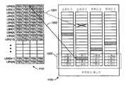
도11은 메타블록의 컴포넌트 멤버들이 논리적 대 물리적 맵핑 테이블(1101)을 이용하여 맵핑될 수 있는 방법을 도시한 것이다. LBN[0]과 관련되는 메모리(1103)내의 메타블록(또는 이 구조를 이용하는 실시예에서 메모리 존) 은 해시 로 표시되는 블록들로 도시된다. (이 예에서) 메모리의 4개의 플레인들은 또 다시 하나 이상의 칩에 걸쳐서 분포될 수 있다. LBN[0] 내에 포함되는 PNB 엔트리들은 해시로 표시되고 메타블록의 부분들인 블록들 각각의 물리적 어드레스들에 관한 것이다. 플레인(0)에 포함되는 메타블록의 제1 멤버는 다른 메타블록 멤버들에 액세스하도록 사용된다. 도5 내지 도10과 관련하여 서술된 바와 같이, 플레인(0)에서 메타블록 멤버는 결함이 있는 것으로 밝혀지면, 전체 메타블록은 결함이 있는 것으로서 표시되는데, 그 이유는 이들이 플레인(0) 상의 멤버를 통해서 메타블록의 나머지에 링크되기 때문이다.11 illustrates how component members of a metablock can be mapped using a logical to physical mapping table 1101. Metablocks (or memory zones in embodiments using this structure) in
맵핑 테이블(1101)은 메타블록들을 형성하기 위한 블록들의 링킹의 레코드의 일 예이다. 메타블록 컴포지션의 적응성을 고려하는 한 가지 기술은, 메타블록이 기록 프로세스에 필요로 될 때마다 이용가능한 양호한 블록들의 풀로부터 메타블록을 동적으로 형성하는 것이다. 이 기술이 메타블록 구조에 대한 적응성을 고려하지만, 블록이 필요로 될 때마다 링킹이 재설정될 필요가 있다. 게다가, 각 플레인은 이 풀을 결정하기 위하여 액세스될 필요가 있다. 본 발명의 주 양상들 중 한 가지 양상을 따르면, 이 레코드는 비휘발성 메모리 내의 위치에 저장된다. 그 후, 이 레코드는 어드레스 변환시 사용하기 위하여 주문형 컨트롤러 상의 플래시 메모리로부터 휘발성 메모리(또는 대안적인 비휘발성 메모리)까지 판독될 수 있다.The mapping table 1101 is an example of a record of linking of blocks to form metablocks. One technique that takes into account the adaptability of the metablock composition is to dynamically form the metablock from a pool of good blocks available whenever the metablock is needed for the recording process. Although this technique considers the adaptability to the metablock structure, the linking needs to be reset whenever a block is needed. In addition, each plane needs to be accessed to determine this pool. According to one of the main aspects of the invention, this record is stored in a location in non-volatile memory. This record can then be read from flash memory on demand controller to volatile memory (or alternative nonvolatile memory) for use in address translation.
한 세트의 실시예들에서, 링킹 정보의 레코드는 사용자 데이터가 저장되는 정상 물리적 블록들 밖의 어느 곳에서와 같이 특수한 비휘발성 메모리 장소에서 유지될 수 있다. 예를 들어, 이 레코드는 도4a의 플레인(0)에서 예약된 에어리어들 중 한 에어리어에 유지되거나 본원에 참조된 미국 특허 공개 2003/0065899에 서술된 바와 같은 배열 내의 시스템 존들 중 임의의 존에서 유지될 수 있다. 또 다른 세트의 실시예들에서, 링킹 정보는 기록된 또는 부분적으로 기록된 블록들을 위한 사용자 데이터 섹터들/제어 데이터 섹터들의 헤더 에어리어에 유지될 수 있다. 소거된 상태에서 블록들에 대해서, 링킹 정보는 비휘발성 메모리 내의 특수한 제어 데이터 에어리어에 저장될 수 있다.In one set of embodiments, a record of linking information may be maintained in a special nonvolatile memory location, such as anywhere outside the normal physical blocks in which user data is stored. For example, this record may be maintained in one of the reserved areas in
이와 같은 테이블을 이용함으로써, 메타블록들로 블록들의 링킹은 결함들을 수용하도록 갱신될 수 있고, 비휘발성 메모리에 레코드를 유지함으로써, 필요로 되는 경우 손쉽게 액세스됨으로써, 배경부에 논의된 종래 기술의 제한을 극복한다.By using such a table, the linking of blocks into metablocks can be updated to accommodate defects, and by keeping a record in non-volatile memory, which is easily accessed if necessary, thereby limiting the prior art discussed in the background. To overcome.
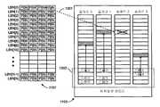
본 발명의 양상의 결함 맵은 플레인(1) 상의 불량 블록을 도시하는 도12에 도시된다. 불량 블록은 "X"로 표시된다. 블록이 결함이 있다라고 밝혀지기 전에, 이 블록을 가리키는 메타블록 LBN[0]의 제2 멤버는 점선의 화살표(1201)로 도시된다. 스페어 블록들(1203)의 콜렉션은 해치로 도시된 동일한 플레인 상에서 이용될 수 있는 스페어를 갖는다. (대안적으로, 스페어가 도5 내지 도10의 프로세스에서 처럼 에러를 발생시키는 또 다른 링킹으로부터 플레인(1)에서 이용될 수 있다면, 이는 스페어들(1203)의 콜렉션으로부터 블록 대신에 사용될 수 있다). 스페어(PBN')의 물리적 블록 번호(PBN)는 불량 블록의 PBN을 대체할 것이다. 따라서, 이 스페어는 화살표(1202)로 도시된 바와 같이 메타블록의 부분이 된다.A defect map of aspects of the present invention is shown in FIG. 12 showing a bad block on
도13은 도11의 맵 구조와 유사한 맵 구조의 예를 도시한 것이다. 도13의 맵 구조는 플레인(2) 상에서 "X"로 표시된 블록상에 도시된 바와 같이 불량 블록, 가능한 성장된 결함을 도시한다. 스페어는 플레인(2) 상의 소거 풀(1302)에서 스페어 블록들의 콜렉션이 스페어들을 갖지 않는 것으로 도시된 바와 같이 불량 블록과 동일한 플레인 상에서 이용될 수 없다. 그러므로, 스페어를 가리키도록 플레인(2) 상의 불량 블록을 재지향시키는 대신에, 메타블록의 나머지와 관련된 물리적 블록들(플레인 0, 1 및 3 상의 블록들)은 3개의 하향 포인팅 화살표들로 도시된 바와 같이 스페어 풀에 부가된다.FIG. 13 shows an example of a map structure similar to that of FIG. The map structure of FIG. 13 shows a bad block, possible grown defects, as shown on a block marked with "X" on
도14는 도11-도13의 데이터 구조를 이용하여 결함 맵을 유지하는 방법의 예를 도시한 것이다. 결함이 검출되거나 부닥치게 되면, 결함의 위치는 물리적 위치 또는 물리적 블록 번호(PBN)를 조사함으로써 결정된다. 스페어 블록이 결함 블록의 물리적 위치와 동일한 플레인에서 이용될 수 있다면, 결함과 관련된 메타블록은 결함있는 블록을 대체하기 위하여 스페어로 지정되는데, 이 후 결함 맵은 갱신된다. 이 시나리오는 도12에 도시되어 있다. 그렇치 않다면, 결함있는 블록과 동일한 플레인에서 남아있는 스페어 블록들이 존재하지 않는다면, 메타블록으로부터 남아있 는 양호한 블록들은 스페어 풀로 지향된다. 이 시나리오는 도13에 도시되어 있다.14 shows an example of a method of maintaining a defect map using the data structure of FIGS. 11-13. If a defect is detected or encountered, the location of the defect is determined by examining the physical location or physical block number (PBN). If a spare block is available in the same plane as the physical location of the defective block, the metablock associated with the defect is designated as a spare to replace the defective block, after which the defect map is updated. This scenario is shown in FIG. Otherwise, if there are no spare blocks remaining in the same plane as the defective block, the good blocks remaining from the metablock are directed to the spare pool. This scenario is shown in FIG.
상술된 바와 같이, 본 발명의 원리적인 양상들 중 한 양상은 컨트롤러가 비휘발성 메모리에서 링킹 테이블의 레코드를 유지하는 것이다. 이 레코드는 도11 내지 도13의 논리적 대 물리적 맵핑 테이블(1101)과 같은 소정의 물리적 어드레스에 대응하는 각 메타블록을 형성하는 블록들의 완전한 리스팅일 수 있다. 대안적으로, 메타블록들로 물리적 블록들의 표준 링킹은 결정론적 알고리즘을 토대로 하며, 비휘발성 메모리에 유지되는 레코드는 링킹 룰로부터의의 임의의 편차들 만을 포함할 필요가 있다. 링킹이 결함들로 인해 갱신되어 결국 표준 링킹으로부터 벗어날 때, 레코드는 이에 대응하여 갱신된다.As mentioned above, one of the principal aspects of the present invention is that the controller maintains a record of the linking table in non-volatile memory. This record may be a complete listing of the blocks that form each metablock corresponding to a given physical address, such as the logical-to-physical mapping table 1101 of Figures 11-13. Alternatively, the standard linking of physical blocks into metablocks is based on a deterministic algorithm, and the record maintained in nonvolatile memory needs to contain only any deviations from the linking rule. When the linking is updated due to defects and eventually deviates from the standard linking, the record is updated correspondingly.
메타블록들로 물리적 블록들을 링킹하기 위하여 사용되는 서술된 메커니즘들은 불량 물리적 블록들의 임의의 분포를 위한 메타블록들의 수를 최대화하여 물리적 블록들이 시스템의 수명 동안 불량일 때 새로운 메타블록들이 생성되도록 한다. 상기와 같이, 메타블록 수는 메타블록에 포함되는 제1 플레인에서 물리적 블록의 어드레스로부터 규정된다.The described mechanisms used to link physical blocks into metablocks maximize the number of metablocks for any distribution of bad physical blocks so that new metablocks are created when the physical blocks are bad for the life of the system. As above, the metablock number is defined from the address of the physical block in the first plane included in the metablock.
"표준" 메타블록은 물리적 블록 어드레스들이 메타블록 수의 결정론적 함수인 물리적 블록들을 포함한다. 예를 들어, 이는 도5-10의 예를 위하여 사용되는 도4b에서 메타블록(MB0)의 배열일 수 있는데, 여기서 표준 메타블록의 모든 블록들은 동일한 로우에 있다. 이 배열은 MBi=(i, i, i, i)로 표시되는데, 괄호안의 n번째 엔트리는 n번째 플레인 내의 블록이 속하는 로우를 표시한다.A "standard" metablock includes physical blocks where the physical block addresses are a deterministic function of the metablock number. For example, this may be an arrangement of metablocks MB0 in FIG. 4B used for the example of FIGS. 5-10, where all blocks of the standard metablock are in the same row. This array is represented by MBi = (i, i, i, i), where the nth entry in parentheses indicates the row to which the block in the nth plane belongs.
또 다른 예에서, 도4b의 메타블록(MB2)의 배열에서 처럼, 물리적 블록 어드레스는 메타블록 수 더하기 물리적 블록이 속하는 플레인의 순차적인 번호와 동일한 오프셋에 의해 제공된다. 즉, 메타블록(i)은 블록들 i+(플레인 수)로 이루어진다. 4개의 블록들의 메타블록에 대해서, 이는 MBi=(i, i+1, i+2, i+3)으로 표시될 수 있다. 이 구조는 도15에 도시되고, 알고리즘 기반으로 한 링킹 테이블을 논의하기 위하여 사용될 것이다. 더욱 일반적으로, 이 알고리즘 기반으로 한 결정론적 링킹은 명백한 방식으로 다음의 다른 수들에 대해 확장을 지닌, 4개의 블록 메타블록의 경우에 대해서 다음과 같이 서술될 것이다.In another example, as in the arrangement of metablock MB2 of FIG. 4B, the physical block address is provided by an offset equal to the number of metablocks plus the sequential number of the plane to which the physical block belongs. That is, metablock i consists of blocks i + (plane number). For a metablock of four blocks, this may be indicated as MBi = (i, i + 1, i + 2, i + 3). This structure is shown in Figure 15 and will be used to discuss the algorithm-based linking table. More generally, this algorithm-based deterministic linking will be described as follows for the case of four block metablocks, with an extension to the following other numbers in an obvious manner.
MBi=(i, f1(i, 플레인 수), f2i, 플레인 수), f3i, 플레인 수))MBi = (i, f1 (i, number of planes), f2 i, number of planes), f3 i, number of planes))
이 표현식에서, i는 로우 수이며, f1, f2 및 f3는 로우 및 플레인 수의 일부 함수들이다. 메타블록 수가 플레인(0)의 로우 수와 동일하다는 협약에 따라서, MB1에서 제1 엔트리는 i가 된다. 도5-10의 예들에 대해서, f1=f2=f3=i인 반면에, 도15에 대해선, f1=f2=f3=i+(플레인 수)이다. 알고리즘 기반으로 한 링킹을 위한 재링킹 프로세스의 논의는 주로 도5-10의 프로세스에서 생략된 버전을 통해서 행해지지만 도15의 표준 링킹을 토대로 행해질 것이다. 컨트롤러는 표준 링킹을 결정하기 위한 펌웨어-기반으로 한 구현방식을 이용할 수 있다.In this expression, i is the number of rows and f1 , f2 and f3 are some functions of the number of rows and planes. In accordance with the convention that the number of metablocks is equal to the number of rows in
물리적 블록들은 가능한 수의 표준 메타블록들을 최대화하는 룰에 따라서 메타블록들로 링크된다. 메타블록이 링크될 때, 표준 블록은 필요로 되는 물리적 블 록이 이용될 수 있는 경우에 생성된다. 표준 메타블록의 형성을 위하여 필요로 되는 임의의 물리적 블록이 불량이면, 메타블록 수는 비사용되는 것으로서 분류된다. 표준 메타블록을 형성하는데 필요로 되는 임의의 물리적 블록이 불량이면, 메타블록 수는 비사용되는 것으로서 분류된다. 이 경우에, 결국 링크되지 않은 채 있는 다른 사용가능한 물리적 블록들은 도15에서 메타블록 n+1에 대해서 도시된 바와 같은 스페어로서 분류된다.Physical blocks are linked into metablocks according to a rule that maximizes the possible number of standard metablocks. When metablocks are linked, standard blocks are created if the required physical blocks are available. If any physical block needed for the formation of a standard metablock is bad, the metablock number is classified as unused. If any physical block needed to form a standard metablock is bad, the metablock number is classified as unused. In this case, other usable physical blocks that eventually remain unlinked are classified as spares as shown for metablock n + 1 in FIG.
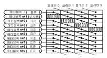
본 발명의 또 다른 양상은 카드상에 결함들의 패턴을 토대로 표준 링킹 패턴을 최적화하거나 그렇치 않다면 사용가능한 표준 메타블록들의 수를 최대화하기 위한 것이다. 카드가 포맷(또는 재포맷화)될 때, 불량 블록들의 패턴은 스캐닝되고 "표준" 링킹 패턴에 관한 판정이 행해져, 이들이 가능한 서로 정합하도록 한다. 많은 경우들에서, 불량 블록 패턴으로의 표준 링킹을 위한 알고리즘의 정합은 필요로 되는 재링크된 메타블록 및 메타 대 물리적 어드레스 변환 오버헤드를 감소시켜, (적어도 초기에) 링킹을 최적화한다. 이의 일 예가 도16 및 도17에 도시된다.Another aspect of the invention is to optimize the standard linking pattern based on the pattern of defects on the card or to maximize the number of standard metablocks available otherwise. When the card is formatted (or reformatted), the pattern of bad blocks is scanned and a determination is made regarding the "standard" linking pattern, so that they match each other as possible. In many cases, matching of algorithms for standard linking to bad block patterns reduces the relinked metablock and meta to physical address translation overhead needed to optimize (at least initially) linking. An example of this is shown in FIGS. 16 and 17.
도16 및 도17은 4개의 불량 물리적 블록들, 즉 각 플레인들(0-3)로부터 하나가 대각선으로 진행하는 예를 고려하자. 불량 블록들의 대각선 패턴의 경우에, 표준 블록들을 위한 최적의 패턴은 또한 도16에 도시된 바와 같이 대각선이 될 것이다. 따라서, 이 예에서, 링크된 블록들이 전혀 존재하지 않음으로, 결국 메타블록들 중 어떤것도 링킹 테이블을 통해서 변환을 필요로 하지 않고 사용가능한 메타블록들의 수는 증가된다. 도17은 표준 링킹이 불량 블록 패턴에 정합하는 것이 아니라 직접 가로지를 때 등가의 상황을 도시한 것이다. 표준 방법이 직접 가로지르는 예에서, 3개의 메타블록들(n+2, n+3 및 n+4)이 재링크될 필요가 있다.16 and 17 consider an example in which four bad physical blocks, i.e., one from each plane (0-3) run diagonally. In the case of a diagonal pattern of bad blocks, the optimal pattern for standard blocks will also be diagonal as shown in FIG. Thus, in this example, since there are no linked blocks at all, none of the metablocks require translation through the linking table and the number of available metablocks is increased. Figure 17 illustrates an equivalent situation when standard linking does not match a bad block pattern but crosses directly. In the example where the standard method crosses directly, three metablocks n + 2, n + 3 and n + 4 need to be relinked.
표준 블록 패턴은 매 카드에 대해서, 매 재포맷팅에 대해서 또는 이들 둘 다에 대해서 특정될 수 있다. 이는 여분의 데이터 보안 레벨을 제공할 수 있는데, 여기서 매 카드는 상이한 블록들을 가로질러 데이터를 스크램블하는 특정 방법을 갖는다. 결국, 표준 메타블록들은 반드시 동일한 구성을 가질 필요는 없지만, 이들은 동일한 룰을 이용하여 형성될 것이다. 또 다른 실시예에서, 호스트는 룰 및 메타블록 링킹 룰을 위한 코드를 제공하길 원함으로, 알고리즘은 시스템 특정되지 않는다.The standard block pattern can be specified for every card, every reformat, or both. This may provide an extra level of data security, where each card has a specific way to scramble data across different blocks. After all, standard metablocks do not necessarily have the same configuration, but they will be formed using the same rules. In another embodiment, the host wants to provide code for rules and metablock linking rules, such that the algorithm is not system specific.
메타블록들이 초기 포맷팅 프로세스 동안 링크될 때, 블록 어드레스 공간의 시작 근처 또는 칩 또는 다이 경계들 근처의 일부 물리적 블록들은 도20에 도시된 바와 같이 표준 메타블록들로 링크될 수 없다. 이들 물리적 블록들은 스페어로서 분류된다. 스페어 물리적 블록들은 스페어 물리적 블록 리스트에 기록된 후, 도9에 서술된 바와 같이 재링크된 메타블록들을 형성하는데 사용될 수 있다.When metablocks are linked during the initial formatting process, some physical blocks near the beginning of the block address space or near chip or die boundaries cannot be linked to standard metablocks as shown in FIG. These physical blocks are classified as spares. The spare physical blocks can be written to the spare physical block list and then used to form relinked metablocks as described in FIG.
표준 블록들로서 존재할 수 없는 메타블록들은 재링크된 메타블록들로서 구조화될 수 있다. 재링크된 메타블록들은 메모리 시스템의 초기 포맷화 프로세스 동안 또는 기존의 메타블록 내에서 물리적 블록의 불량에 응답하여 형성될 수 있다. 도19의 메타블록(n+4)은 표준 메타블록으로서 링크될 수 없는데, 그 이유는 플레인(2)에서 필요로 되는 물리적 블록이 불량이기 때문이다. 이 경우에, 재링크된 메타블록은 플레인(2)에서 스페어 물리적 블록을 대체함으로써 생성된다. 불량 물리적 블록 대신에 재링크되는 스페어 물리적 블록은 불량 블록과 동일한 플레인 에 바람직하게 위치되어 메타블록 내에서 프로그래밍 병렬화를 유지한다.Metablocks that cannot exist as standard blocks may be structured as relinked metablocks. Relinked metablocks may be formed in response to a failure of a physical block during the initial formatting process of the memory system or within an existing metablock. The metablock (n + 4) in Fig. 19 cannot be linked as a standard metablock because the physical block required in the
바람직한 실시예에서, 또 다른 다이 또는 칩으로 가로질러 진행하는 재링킹이 부가적인 다이/칩 판독들 또는 프로그램들을 트리거 할 수 있을 때 동일한 다이 또는 칩 내에서만 블록들을 재링크하는 것이 바람직하다. 예를 들어, 메타-블록이 2개의 플레인들 각각을 갖는 2개의 칩들에 걸쳐있는 4-플레인 메타-블록의 전형적인 경우에, 데이터는 모두 4개의 플레인들(또는 이 플레인들로부터 판독)로 프로그램될 수 있는데, 이는 병렬로 2칩 판독/프로그램을 필요로 한다. (이는 100% 병렬이 아니라 파이프라인이 아님으로, 페이지 판독, 블록 프로그램 및 소거는 병렬로 행해질 수 있지만, 데이터 전달이 병렬이 되지 않도록 데이터 버스는 공유된다). 이 경우에, 메타블록이 재링크되어 물리적 블록이 다른 2개와 동시에 액세스할 수 없는 또 다른 제3 칩으로부터 취해지도록 하고 동작 시간이 2배가 될 수 있도록 한다.In a preferred embodiment, it is desirable to relink blocks only within the same die or chip when relinking that proceeds across another die or chip can trigger additional die / chip reads or programs. For example, in a typical case of a four-plane meta-block in which the meta-block spans two chips with two planes each, the data will be programmed in all four planes (or read from these planes). This requires two chip read / program in parallel. (This is not a 100% parallel, but a pipeline, so page reads, block programs, and erases can be done in parallel, but the data bus is shared so that data transfers are not parallel). In this case, the metablock is relinked so that the physical block is taken from another third chip that cannot be accessed simultaneously with the other two and the operation time can be doubled.
플레인(0)에서 불량 물리적 블록이 플레인(0)으로부터 스페어 블록으로 대체되면, 메타블록 수는 도20의 메타블록에 대해서 도시된 바와 같이 스페어 블록의 수로 규정된다. 재링크된 메타블록들은 다음의 물리적 블록 불량의 이벤트에서 부가적으로 재링크될 수 있다. 표준 메타블록들로서 링크될 수 없는 어드레스 공간의 최상부에 근접한 메타블록들은 재링크된 메타블록들의 형태를 취할 수 있다.If the bad physical block in
도4d와 관련하여 상술된 바와 같이, 블록 플레인들 및 칩들에 걸쳐서 뿐만 아니라 소정 플레인 내의 깊이에서 블록을 링크하는 2차원 메타-블록들을 이용하는 구성들이 또한 존재한다. 도21은 2차원 경우에서 재링킹의 예를 도시한 것이다. 도21에서, "2-D 메타블록"은 2*4 메타블록의 예이다. 수행면에서 최대 이점은 모두 8개의 블록들이 병렬로 액세스될 수 있을 때 성취될 수 있다. 1-D 링킹 방법들의 주 링킹 및 재-링킹 원리들은 또한 적용되지만 어떤 확장들을 갖는다. 도면에서 알 수 있는 바와 같이, 플레인 내의 물리적 블록들 중 임의의 블록에서 불량 물리적 블록은 메타블록(n)에 대해서 도시된 바와 같이 비사용되는 메타블록을 발생시킨다. 2-D 메타블록이 재링크될 때, 플레인(2)에서 메타블록 (n+2)의 상부 블록에 대해서, 소정 플레인에서 불량 물리적 블록만이 대체될 필요가 있다. 예를 들어, 플레인(2)에서 메타블록 (n+2)의 상부 블록에 대해서, 재링크되는 반면, 플레인(2)에서 메타블록(n+2)의 하부 블록은 존재하지 않는다.As described above with respect to FIG. 4D, there are also configurations that use two-dimensional meta-blocks that link the block at depths within a given plane as well as across block planes and chips. Figure 21 shows an example of relinking in the two-dimensional case. In Fig. 21, "2-D metablock" is an example of a 2 * 4 metablock. The maximum benefit in terms of performance can be achieved when all eight blocks can be accessed in parallel. The main linking and re-linking principles of 1-D linking methods also apply but have some extensions. As can be seen in the figure, a bad physical block in any of the physical blocks in the plane generates an unused metablock as shown for metablock n. When the 2-D metablock is relinked, for the upper block of metablock (n + 2) in
표준 링킹으로부터의 편차들만이 비휘발성 메모리 내의 레코드에 유지되는 실시예에서, 메타블록 링킹을 위한 관리 데이터 구조들은 플래시 메모리 내의 하나 이상의 전용 블록 링키지 관리 블록들 내의 2가지 유형들의 섹터들 내에 포함될 수 있다. 이 배열은 완전한 링킹을 세이브하는 것과 관련하여 더 적은 정보의 저장을 필요로 한다는 이점을 갖는다. 메모리 시스템에서 매 재링크되는 메타블록의 메타블록 수들은 링크 테이블 섹터들의 세트 내의 링크 테이블에 포함된다. 표준 메타블록들에 대한 엔트리들이 링크 테이블에 저장될 필요가 없는데, 그 이유는 이들의 물리적 블록 어드레스들이 메타블록 수로부터 결정론적으로 발생되기 때문이다. RF(재링크된) 플래그는 메타-블록의 속성으로서 사용되어, 블록이 표준이고, 모든 블록들이 표준 방식으로 링크되는지를 나타내거나, 이것이 재링크되고 링크 테이블(LT)를 통해서 부가적인 블록 어드레스 변환을 필요로 하는지를 나타낸다. RF 플래그는 LT를 분석함으로써 결정될 수 있고, 그 후, SRAM에 저장되거나, 그 밖에 메타-블록에 대한 속성으로서 주 비휘발성 메모리 내의 제어 데이터 구조에 저장될 수 있다. 대안적으로, 재링크된 섹터들의 리스트는 어느 메타-블록들이 재링크되는지를 결정하기 위하여 탐색될 수 있는 리스트에 유지될 수 있다. 링크 테이블 내의 엔트리들은 메타블록 수로 순서화될 수 있고, 각 엔트리는 메타블록 수에 대한 필드들 및 각 링크된 물리적 블록의 블록 어드레스를 갖는다.In an embodiment where only deviations from standard linking are maintained in a record in nonvolatile memory, management data structures for metablock linking may be included in two types of sectors in one or more dedicated block linkage management blocks in flash memory. . This arrangement has the advantage of requiring less storage of information with respect to saving complete linking. The metablock numbers of metablocks that are relinked every time in the memory system are included in the link table in the set of link table sectors. Entries for standard metablocks need not be stored in the link table because their physical block addresses are deterministically derived from the metablock number. The RF (relinked) flag is used as an attribute of the meta-block, indicating whether the block is standard and whether all blocks are linked in a standard way, or is it relinked and additional block address translation through the link table (LT) Indicates if it needs The RF flag may be determined by analyzing the LT and then stored in the SRAM, or else stored in the control data structure in the main nonvolatile memory as an attribute for the meta-block. Alternatively, the list of relinked sectors may be maintained in a list that can be searched to determine which meta-blocks are relinked. Entries in the link table may be ordered by the number of metablocks, each entry having fields for the number of metablocks and the block address of each linked physical block.
이 링크 테이블 구조의 확장에서, 표준 링킹을 설정하는 기본 알고리즘으로부터의 편차들 자체는 한 세트의 룰들을 토대로 할 수 있는데, 예를 들어, 비표준 링킹은 단일 플레인으로 제한될 수 있거나 블록이 원래의 로우로부터 얼마나 멀리 재링크될 수 있는지를 제한할 수 있다. 재링킹이 모든 알고리즘들에 대해서 예외적일 때에만, 명백히 이는 비휘발성 메모리에 유지될 필요가 있다.In this extension of the link table structure, the deviations from the basic algorithm that sets up the standard linking itself may be based on a set of rules, for example, the non-standard linking may be limited to a single plane or the block may be intact. You can limit how far you can relink from. Only when relinking is exceptional for all algorithms, obviously it needs to be kept in nonvolatile memory.
링크 테이블의 특정 예 및 포함되는 정보가 압출될 수 있는 방법이 도22 및 표1과 관련하여 서술된다. 링크 테이블 섹터는 카드 내에서 재링크되는 블록들에 관한 정보를 유지한다. 카드의 크기 및 각 다이 내의 불량 블록들의 수에 따라서, 하나 이상의 테이블 섹터가 존재할 수 있는데, 이는 부트 블록(Boot Block)에 저장될 수 있다. 상술된 바와 같이, 메타-블록들은 링킹을 위한 표준 방법을 갖고 블록들 중 한 블록이 불량이면, 메타-블록은 동일한 플레인에서 스페어 물리적 블록과 재링크될 수 있다. 링크 테이블들 섹터들은 정보를 저장하는데, 이 정보에 관한 블록들이 재링킹에 사용된다. 도22는 메타-블록들의 재링킹의 또 다른 예이다.Specific examples of link tables and how the information included can be extruded are described with reference to FIGS. 22 and 1. The link table sector maintains information about blocks that are relinked within the card. Depending on the size of the card and the number of bad blocks in each die, there may be one or more table sectors, which may be stored in a boot block. As mentioned above, if the meta-blocks have a standard method for linking and one of the blocks is bad, the meta-block can be relinked with the spare physical block in the same plane. Link tables sectors store information, which blocks are used for relinking. 22 is another example of relinking of meta-blocks.
도22에 도시된 메타블록들 중, 단지 메타블록 (0) 만이 8개의 플레인들을 가 로질러 직선으로 취해지는 표준 링킹을 갖는다. 이 도면은 여러 블록 링킹 상황들을 도시한다.Of the metablocks shown in FIG. 22, only metablock (0) has a standard linking that is taken straight across the eight planes. This figure illustrates several block linking situations.
A. 메타블록 0은 재링키이 없는 표준 메타블록임으로 링크 테이블 섹터에서 나타나지 않는다.
B. 메타블록 1은 플레인들 0* 및 1에서 2개의 불량 블록들을 갖는다.
C. 메타블록 4는 플레인들 0* 및 5에서 2개의 불량 블록들을 갖는다.
D. 메타블록 5는 플레인들 1, 3 및 4에서 3개의 불량 블록들을 갖는다.
E. 메타블록 7은 플레인 0*에서 하나의 불량 블록을 갖는다.
F. 메타블록 9는 기존의 스페어 물리적 블록들로부터 완전히 재링크되지만, 플레인들 0 및 7내의 블록들이 원래 메타-블록으로부터 나온다.
이 경우들에서, 재링킹이 플레인 0에서 불량 블록으로 인한 것인 경우에 *로 표시된다. 이 경우에, 물리적 어드레스는 원래 메타블록이 존재하는 위치에 관한 것이다. 도22의 예에서 많은 수의 불량 블록들로 인해, 메타블록들 (2, 3, 6 또는 7)은 존재하지 않는다.In these cases, it is marked with * when the relinking is due to bad blocks in plane zero. In this case, the physical address relates to the location where the original metablock exists. Due to the large number of bad blocks in the example of Fig. 22,
도22에 도시된 블록 재링킹을 위하여 사용되는 압축 알고리즘이 표1에서 처럼 규정된다.The compression algorithm used for block relinking shown in Fig. 22 is defined as in Table 1.

표 1Table 1
임의의 링크 테이블 엔트리의 크기는 다음과 같이 규정될 수 있다.The size of any link table entry may be defined as follows.
바이트의 수 = 3+(3 * 재링크된 블록의 수)Number of bytes = 3+ (3 * number of relinked blocks)
예를 들어, 메타블록(1)에 대해서, 제1의 3개의 바이트들은 메타블록(1)을 식별하고 이는 2개의 재링킹들을 갖는데, 3바이트는 이들 재링킹들 각각을 규정하기 위하여 할당된다. 이 재링킹들은 재링크된 블록이 (1바이트)에 대응하는 8개의 플레인들 중 어느 플레인 및 재링크되는 로우 수에 의해 특정된다.For example, for
링크 테이블 내의 엔트리들의 전체 세트는 다수의 링크 테이블 섹터들에 걸쳐서 확산될 수 있다. 링크 테이블 섹터는 블록 링키지 관리 블록에서 다음 이용가능한 섹터 위치에 이를 기록함으로써 생성되거나 수정될 수 있다. 그러므로, 링크 테이블 섹터의 다수의 복제들이 존재하는데, 단지 최근의 버전만이 유효하다. 블록 링키지 관리 블록에서 유효 링크 테이블 섹터들의 위치들로의 인덱스는 후술되는 블록 링키지 관리 블록에서 스페어 물리적 블록 리스트 섹터 내의 필드에 포함될 수 있다. 각 유효 링크 테이블 섹터 내의 제1 엔트리에 관계하는 메타블록 수는 컨트롤러 RAM 내의 리스트에 유지되어, 임의의 메타블록 수에 대한 관련 링크 테이블 섹터의 식별을 용이하게 한다. 부가적인 엔트리가 최대 엔트리들의 수를 이미 포함하는 링크 테이블 섹터에 부가되어야만 하면, 이 섹터는 엔트리들의 절반을 각각 갖는 2개의 새로운 섹터들로 분리되고 새로운 엔트리는 적절한 새로운 색터에 삽입된다.The entire set of entries in the link table can be spread across multiple link table sectors. The link table sector can be created or modified by writing it to the next available sector location in the block linkage management block. Therefore, there are multiple copies of the link table sector, only the latest version is valid. The index to locations of valid link table sectors in the block linkage management block may be included in a field in the spare physical block list sector in the block linkage management block described below. The number of metablocks associated with the first entry in each valid link table sector is maintained in a list in the controller RAM to facilitate the identification of the associated link table sectors for any number of metablocks. If an additional entry must be added to a link table sector that already contains the maximum number of entries, this sector is split into two new sectors each having half of the entries and the new entry is inserted into the appropriate new sector.
모든 스페어 물리적 블록들의 블록 어드레스들은 스페어 물리적 블록 리스트 섹터 내의 순서화되지 않은 리스트에서 엔트리들로서 유지된다. 일부 실시예들에서, 칩 당 플레인 당 최대 스페어 블록들의 수를 제한하는 것이 간편할 수 있다. 전형적인 실시예에서, 이는 16으로 제한되는데, 대부분의 경우들에 이는 충분히 크게되어야 한다. 플레인에서 16개 이상의 스페어 블록들이 존재하면, 이들은 "상실"될 것이다.The block addresses of all spare physical blocks are maintained as entries in an unordered list in the spare physical block list sector. In some embodiments, it may be convenient to limit the maximum number of spare blocks per plane per chip. In a typical embodiment, this is limited to 16, which in most cases should be large enough. If there are more than 16 spare blocks in the plane, they will be "lost".
표준 메타블록이 메타블록들 내로의 플래시 메모리의 초기 구성동안 생성될 수 없기 때문에 또는 표준 또는 재링크된 메타블록으로 링크되는 물리적 블록이 불량이기 때문에, 스페어가 되는 블록들은 스페어 물리적 블록 리스트의 끝에 새로운 엔트리들로서 부가된다. 스페어 블록이 재링크된 메타블록의 생성을 위하여 필요로 될 때, 스페어 물리적 블록 리스트의 시초에 가장근접한 관련 플레인 내의 제1 블록이 사용될 수 있다. 스페어 물리적 블록 리스트 섹터는 또한 유효한 링크 테이블 섹터 위치들에 대한 인덱스를 갖는 필드를 포함한다.Because the standard metablock cannot be created during the initial configuration of flash memory into metablocks or because the physical block that is linked to the standard or relinked metablock is bad, the blocks becoming spares are new at the end of the spare physical block list. Added as entries. When a spare block is needed for the generation of a relinked metablock, the first block in the relevant plane closest to the beginning of the spare physical block list may be used. The spare physical block list sector also includes a field with an index to valid link table sector locations.
메타블록 재링크 동작이 발생되고 링크 테이블 섹터들이 생성되거나 수정될 때, 스페어 물리적 블록 리스트 및 링크 테이블 섹터 인덱스 필드들 둘 다는 스페어 물리적 블록 리스트 섹터에서 수정될 수 있다. 그러므로, 유효 스페어 물리적 블록 리스트 섹터는 블록 링키지 관리 블록에서 최종 기록된 섹터이다. 블록 링키지 관리 블록이 채워질 때, 이는 모든 유효 섹터들을 새로운 블록 위치로 재기록함으로써 제어 기록 동작 동안 콤팩트하게 될 수 있고 전체 블록은 다음에 소거될 수 있다.When a metablock relink operation occurs and link table sectors are created or modified, both the spare physical block list and the link table sector index fields can be modified in the spare physical block list sector. Therefore, the valid spare physical block list sector is the last recorded sector in the block linkage management block. When the block linkage management block is filled, it can be made compact during the control write operation by rewriting all valid sectors to a new block position and the entire block can be erased next.
스페어 물리적 블록 섹터들의 세이브를 간단히 하고 대체 블록을 찾을 때 필요로 되는 탐색 량을 제한하기 위하여, 스페어 물리적 블록 리스트는 칩, 다이, 및 플레인에 의해 저장될 수 있다. 필요로 되는 실제 섹터들의 수는 메모리 장치의 크기, 장치들의 수 및 사용되는 인터리빙 방법에 좌우된다. 상술된 바와 같이, 플레인 당 단지 특정 수의 물리적 블록들을 저장하는 것이 간편하게 될 수 있다. 유지되는 이 수는 플레인 당 블록들의 수 및 블록들의 예측된 불량 레이트에 좌우될 것이다. 이는 각 스페어 물리적 블록 리스트 섹터가 여러 플레인들에 대해서 스페어 물리적 블록들을 유지한다는 것을 의미한다. 펌웨어는 로딩하기 위하여 정확한 섹터를 계산하고 나서 이 정확한 값들을 로딩하기 위하여 섹터 내로 인덱스할 것이다.In order to simplify the save of spare physical block sectors and limit the amount of search required to find replacement blocks, the spare physical block list may be stored by chips, dies, and planes. The actual number of sectors required depends on the size of the memory device, the number of devices and the interleaving method used. As mentioned above, it may be convenient to store only a certain number of physical blocks per plane. This number maintained will depend on the number of blocks per plane and the predicted failure rate of the blocks. This means that each spare physical block list sector holds spare physical blocks for several planes. The firmware will calculate the correct sector to load and then index into the sector to load these correct values.
스페어 물리적 블록 리스트들의 수가 재링킹으로 인해 변화되거나 또 다른 불량 블록이 발견될 때, 새로운 스페어 물리적 블록 리스트 섹터가 기록될 것이다.이는 동일한 물리적 에어리어를 커버하는 2개의 스페어 물리적 블록 리스트 섹터들을 의미할 수 있다. 부트 섹터는 유효 섹터의 인덱스를 포함하는 스페어 물리적 블 록 리스트 인덱스들을 유지한다. 스페어 물리적 블록들이 스페어 물리적 블록 리스트에 의해 커버되는 에어리어에 존재하면, 이 섹터는 부트 블록에 존재하지 않을 것이다.When the number of spare physical block lists changes due to relinking or another bad block is found, a new spare physical block list sector will be written. This may mean two spare physical block list sectors covering the same physical area. have. The boot sector maintains spare physical block list indices, including the index of the valid sector. If the spare physical blocks are in an area covered by the spare physical block list, this sector will not be in the boot block.
도22를 다시 참조하면, 이는 8 웨이 인터리빙된 카드와 관계한다. 그러므로, 모든 스페어 물리적 블록 리스트 정보를 유지하기 위해선 적어도 8개의 어레이들이 존재하여야 만 할 것이다. 카드상의 모든 다음 다이에 대해서, 부가적인 8개의 어레이들이 필요로 될 것이다. 도22에 대응하는 스페어 물리적 블록 리스트는 표2에 나타나 있다.Referring again to Figure 22, this relates to an 8 way interleaved card. Therefore, at least eight arrays must be present to maintain all spare physical block list information. For every next die on the card, an additional eight arrays will be needed. The spare physical block list corresponding to FIG. 22 is shown in Table 2.

표 2TABLE 2
링킹 테이블에 따라서, 스페어 물리적 블록 리스트는 주문형 휘발성 RAM내로 캐쉬될 수 있는 비휘발성 메모리에 테이블로서 저장될 수 있다.Depending on the linking table, the spare physical block list can be stored as a table in nonvolatile memory that can be cached into on-demand volatile RAM.
본 발명의 각종 양상들이 펌웨어 기반으로 한 구현방식과 관련하여 서술되었지만, 이들은 또한 하드웨어 기반으로 한 구현방식으로 구현될 수 있다. 컨트롤러 상의 또는 바람직하게는 메모리 칩 자체상의 하드웨어 엔진은 재링킹을 행할 수 있다. 이 재링킹 정보는 칩 차제상에 특수용 메모리 위치에 저장될 수 있다. 그 후, 이 컨트롤러는 표준으로서 모든 블록들을 처리할 수 있고, 엔진은 블록 어드레스들 을 실제 내부 어드레스들로 변환될 것이다. 더 작은 블록 구조들 또는 임의의 재링킹 상세사항들 중 어느 하나에 관해서 인지함이 없이도 메모리는 단지 표준 블록들을 지닌 메모리서 또는 큰 물리적 호스트들을 갖는 메모리로서 호스트(또는 컨트롤러)에 나타날 것이다.Although various aspects of the invention have been described with reference to firmware-based implementations, they can also be implemented with hardware-based implementations. The hardware engine on the controller or preferably on the memory chip itself can perform relinking. This relinking information can be stored in a special memory location on the chip breakdown. The controller can then process all blocks as a standard, and the engine will translate the block addresses into actual internal addresses. Without knowing about either the smaller block structures or any relinking details, the memory will only appear to the host (or controller) in memory with standard blocks or as memory with large physical hosts.
본 발명의 각종 양상들의 특정 예들이 서술되었지만, 본 발명은 첨부된 청구범위 내에서 보호된다는 것을 이해할 것이다.While specific examples of various aspects of the invention have been described, it will be understood that the invention is protected within the scope of the appended claims.
Claims (43)
Translated fromKoreanApplications Claiming Priority (2)
| Application Number | Priority Date | Filing Date | Title |
|---|---|---|---|
| US10/750,157US20050144516A1 (en) | 2003-12-30 | 2003-12-30 | Adaptive deterministic grouping of blocks into multi-block units |
| US10/750,157 | 2003-12-30 |
Publications (1)
| Publication Number | Publication Date |
|---|---|
| KR20060120231Atrue KR20060120231A (en) | 2006-11-24 |
Family
ID=34701162
Family Applications (1)
| Application Number | Title | Priority Date | Filing Date |
|---|---|---|---|
| KR1020067013306AWithdrawnKR20060120231A (en) | 2003-12-30 | 2004-12-15 | Adaptive Deterministic Grouping of Blocks into Multiple Block Units |
Country Status (9)
| Country | Link |
|---|---|
| US (3) | US20050144516A1 (en) |
| EP (1) | EP1700313B1 (en) |
| JP (1) | JP4960705B2 (en) |
| KR (1) | KR20060120231A (en) |
| CN (1) | CN1930635B (en) |
| AT (1) | ATE451694T1 (en) |
| DE (1) | DE602004024582D1 (en) |
| TW (1) | TWI294081B (en) |
| WO (1) | WO2005066974A1 (en) |
Cited By (9)
| Publication number | Priority date | Publication date | Assignee | Title |
|---|---|---|---|---|
| KR101269557B1 (en)* | 2011-05-20 | 2013-06-04 | 연세대학교 산학협력단 | A semiconductor memory reparing device and a repairing method thereof |
| KR101372245B1 (en)* | 2007-08-30 | 2014-03-10 | 삼성전자주식회사 | Architecture of memory cell array, non-volatile memory device having the same, and method of constructing a memory cell array |
| KR101399549B1 (en)* | 2007-09-04 | 2014-05-28 | 삼성전자주식회사 | Semiconductor memory devices and block management method thereof |
| US8904088B2 (en) | 2008-09-30 | 2014-12-02 | Samsung Electronics Co., Ltd. | Method of managing a solid state drive, associated systems and implementations |
| KR20180047329A (en)* | 2016-10-31 | 2018-05-10 | 에스케이하이닉스 주식회사 | Memory system and opration method for the same |
| US10628067B2 (en) | 2017-12-15 | 2020-04-21 | SK Hynix Inc. | Memory system and operating method thereof |
| KR20200048978A (en)* | 2018-10-31 | 2020-05-08 | 에스케이하이닉스 주식회사 | Data storage device and operating method thereof |
| KR20200060053A (en)* | 2018-11-22 | 2020-05-29 | 에스케이하이닉스 주식회사 | Memory system and operation method thereof |
| US11537483B2 (en) | 2019-08-08 | 2022-12-27 | SK Hynix Inc. | Controller for managing superblocks and operation method thereof |
Families Citing this family (207)
| Publication number | Priority date | Publication date | Assignee | Title |
|---|---|---|---|---|
| US8027194B2 (en) | 1988-06-13 | 2011-09-27 | Samsung Electronics Co., Ltd. | Memory system and method of accessing a semiconductor memory device |
| JP4284200B2 (en)* | 2004-01-28 | 2009-06-24 | 株式会社東芝 | Nonvolatile semiconductor memory system |
| US7464306B1 (en) | 2004-08-27 | 2008-12-09 | Lexar Media, Inc. | Status of overall health of nonvolatile memory |
| EP1630657A1 (en)* | 2004-08-30 | 2006-03-01 | STMicroelectronics S.r.l. | Embedded storage device with integrated data-management functions and storage system incorporating it |
| US7315917B2 (en)* | 2005-01-20 | 2008-01-01 | Sandisk Corporation | Scheduling of housekeeping operations in flash memory systems |
| EP1712985A1 (en)* | 2005-04-15 | 2006-10-18 | Deutsche Thomson-Brandt Gmbh | Method and system for storing logical data blocks into flash-blocks in multiple non-volatile memories which are connected to at least one common data I/O bus |
| US7552271B2 (en)* | 2005-08-03 | 2009-06-23 | Sandisk Corporation | Nonvolatile memory with block management |
| DE602006019263D1 (en)* | 2005-08-03 | 2011-02-10 | Sandisk Corp | NON-VOLATILE MEMORY WITH BLOCK ADMINISTRATION |
| US7558906B2 (en)* | 2005-08-03 | 2009-07-07 | Sandisk Corporation | Methods of managing blocks in nonvolatile memory |
| US7984084B2 (en)* | 2005-08-03 | 2011-07-19 | SanDisk Technologies, Inc. | Non-volatile memory with scheduled reclaim operations |
| US7536627B2 (en) | 2005-12-27 | 2009-05-19 | Sandisk Corporation | Storing downloadable firmware on bulk media |
| US7546515B2 (en) | 2005-12-27 | 2009-06-09 | Sandisk Corporation | Method of storing downloadable firmware on bulk media |
| WO2007077595A1 (en)* | 2005-12-28 | 2007-07-12 | Fujitsu Limited | Method, program, and apparatus for controlling memory |
| US7441068B2 (en) | 2006-01-06 | 2008-10-21 | Phison Electronics Corp. | Flash memory and method for utilizing the same |
| US7774643B2 (en)* | 2006-01-06 | 2010-08-10 | Dot Hill Systems Corporation | Method and apparatus for preventing permanent data loss due to single failure of a fault tolerant array |
| GB2434460B (en)* | 2006-01-24 | 2007-12-05 | Phison Electronics Corp | Flash memory and method for utilizing the same |
| KR100703807B1 (en)* | 2006-02-17 | 2007-04-09 | 삼성전자주식회사 | Method and apparatus for managing blocks according to change type of data in block type memory |
| KR100675015B1 (en)* | 2006-02-24 | 2007-01-29 | 삼성전자주식회사 | Built-in memory device with scan function and column redundancy, redundancy repair and scanning method |
| JP4171749B2 (en)* | 2006-04-17 | 2008-10-29 | Tdk株式会社 | Memory controller and flash memory system |
| US20080010510A1 (en)* | 2006-06-19 | 2008-01-10 | Tony Turner | Method and system for using multiple memory regions for redundant remapping |
| US20080052446A1 (en)* | 2006-08-28 | 2008-02-28 | Sandisk Il Ltd. | Logical super block mapping for NAND flash memory |
| KR100784007B1 (en)* | 2006-10-31 | 2007-12-10 | 주식회사 하이닉스반도체 | Nonvolatile Memory Device and Erasing Method |
| KR100809069B1 (en)* | 2006-11-03 | 2008-03-03 | 삼성전자주식회사 | Optical media drive having nonvolatile memory and its driving method |
| US20080162787A1 (en)* | 2006-12-28 | 2008-07-03 | Andrew Tomlin | System for block relinking |
| US20080162612A1 (en)* | 2006-12-28 | 2008-07-03 | Andrew Tomlin | Method for block relinking |
| WO2008082950A1 (en)* | 2006-12-28 | 2008-07-10 | Sandisk Corporation | System for block relinking |
| US7468920B2 (en) | 2006-12-30 | 2008-12-23 | Sandisk Corporation | Applying adaptive body bias to non-volatile storage |
| US7669092B2 (en)* | 2007-02-26 | 2010-02-23 | Micron Technology, Inc. | Apparatus, method, and system of NAND defect management |
| DE112007003388T5 (en)* | 2007-03-21 | 2009-12-24 | Intel Corporation, Santa Clara | Method for managing sectors of a non-volatile memory |
| US7535764B2 (en)* | 2007-03-21 | 2009-05-19 | Sandisk Corporation | Adjusting resistance of non-volatile memory using dummy memory cells |
| US20090006436A1 (en)* | 2007-06-29 | 2009-01-01 | Alqudah Yazan A | Automated yield analysis system |
| US20090013148A1 (en)* | 2007-07-03 | 2009-01-08 | Micron Technology, Inc. | Block addressing for parallel memory arrays |
| US9373362B2 (en)* | 2007-08-14 | 2016-06-21 | Dell Products L.P. | System and method for implementing a memory defect map |
| KR20090021476A (en)* | 2007-08-27 | 2009-03-04 | 삼성전자주식회사 | Memory cell array, non-volatile memory device comprising same and method of configuring memory cell array |
| US7818493B2 (en)* | 2007-09-07 | 2010-10-19 | Sandisk Corporation | Adaptive block list management |
| KR20090026941A (en)* | 2007-09-11 | 2009-03-16 | 삼성전자주식회사 | Method and apparatus for performing address mapping in a virtual file system of a storage device having a plurality of nonvolatile data storage media |
| US8566504B2 (en)* | 2007-09-28 | 2013-10-22 | Sandisk Technologies Inc. | Dynamic metablocks |
| US8762620B2 (en)* | 2007-12-27 | 2014-06-24 | Sandisk Enterprise Ip Llc | Multiprocessor storage controller |
| TW200931425A (en)* | 2008-01-11 | 2009-07-16 | Phison Electronics Corp | Method for managing flash memory blocks and controller using the same |
| JP5032371B2 (en) | 2008-03-01 | 2012-09-26 | 株式会社東芝 | Memory system |
| JP5010505B2 (en)* | 2008-03-01 | 2012-08-29 | 株式会社東芝 | Memory system |
| WO2009140157A2 (en)* | 2008-05-15 | 2009-11-19 | Board Of Governors Of Higher Education, State Of Rhode Island And Providence Plantations | Systems and methods for recovering information from nand gate array memory systems |
| US8074023B2 (en)* | 2008-05-22 | 2011-12-06 | Nuvoton Technology Corporation | In-system programming to switch memory access from one area to another in memory cards |
| US7971007B2 (en)* | 2008-07-08 | 2011-06-28 | Silicon Motion, Inc. | Downgrade memory apparatus, and method for accessing a downgrade memory |
| KR101103061B1 (en)* | 2008-07-28 | 2012-01-06 | 주식회사 팍스디스크 | Semiconductor storage system and its control method |
| JP4632180B2 (en) | 2008-10-15 | 2011-02-16 | Tdk株式会社 | MEMORY CONTROLLER, FLASH MEMORY SYSTEM HAVING MEMORY CONTROLLER, AND FLASH MEMORY CONTROL METHOD |
| JP4720891B2 (en)* | 2008-09-30 | 2011-07-13 | Tdk株式会社 | MEMORY CONTROLLER, FLASH MEMORY SYSTEM HAVING MEMORY CONTROLLER, AND FLASH MEMORY CONTROL METHOD |
| US8214579B2 (en) | 2008-09-30 | 2012-07-03 | Tdk Corporation | Memory controller, flash memory system with memory controller, and method of controlling flash memory |
| JP4582232B2 (en)* | 2008-09-30 | 2010-11-17 | Tdk株式会社 | MEMORY CONTROLLER, FLASH MEMORY SYSTEM HAVING MEMORY CONTROLLER, AND FLASH MEMORY CONTROL METHOD |
| JP2010092200A (en)* | 2008-10-07 | 2010-04-22 | Tdk Corp | Memory controller, flash memory system equipped with memory controller and method of controlling flash memory |
| US7962801B2 (en)* | 2008-10-15 | 2011-06-14 | Silicon Motion, Inc. | Link table recovery method |
| US8244960B2 (en)* | 2009-01-05 | 2012-08-14 | Sandisk Technologies Inc. | Non-volatile memory and method with write cache partition management methods |
| US8700840B2 (en)* | 2009-01-05 | 2014-04-15 | SanDisk Technologies, Inc. | Nonvolatile memory with write cache having flush/eviction methods |
| US8040744B2 (en)* | 2009-01-05 | 2011-10-18 | Sandisk Technologies Inc. | Spare block management of non-volatile memories |
| US20100174845A1 (en)* | 2009-01-05 | 2010-07-08 | Sergey Anatolievich Gorobets | Wear Leveling for Non-Volatile Memories: Maintenance of Experience Count and Passive Techniques |
| US8094500B2 (en)* | 2009-01-05 | 2012-01-10 | Sandisk Technologies Inc. | Non-volatile memory and method with write cache partitioning |
| US8261174B2 (en) | 2009-01-13 | 2012-09-04 | International Business Machines Corporation | Protecting and migrating memory lines |
| JP4762323B2 (en) | 2009-03-03 | 2011-08-31 | 富士通株式会社 | Access control apparatus, information processing apparatus, access control program, and access control method |
| US8095765B2 (en) | 2009-03-04 | 2012-01-10 | Micron Technology, Inc. | Memory block management |
| US8239614B2 (en) | 2009-03-04 | 2012-08-07 | Micron Technology, Inc. | Memory super block allocation |
| US8868809B2 (en)* | 2009-11-30 | 2014-10-21 | Lsi Corporation | Interrupt queuing in a media controller architecture |
| US8321639B2 (en)* | 2009-12-30 | 2012-11-27 | Lsi Corporation | Command tracking for direct access block storage devices |
| US8245112B2 (en)* | 2009-06-04 | 2012-08-14 | Lsi Corporation | Flash memory organization |
| US20100306451A1 (en)* | 2009-06-01 | 2010-12-02 | Joshua Johnson | Architecture for nand flash constraint enforcement |
| US8555141B2 (en)* | 2009-06-04 | 2013-10-08 | Lsi Corporation | Flash memory organization |
| US8166258B2 (en)* | 2009-07-24 | 2012-04-24 | Lsi Corporation | Skip operations for solid state disks |
| US8219776B2 (en)* | 2009-09-23 | 2012-07-10 | Lsi Corporation | Logical-to-physical address translation for solid state disks |
| US8516264B2 (en)* | 2009-10-09 | 2013-08-20 | Lsi Corporation | Interlocking plain text passwords to data encryption keys |
| KR101600951B1 (en)* | 2009-05-18 | 2016-03-08 | 삼성전자주식회사 | Solid state drive device |
| US7856528B1 (en) | 2009-08-11 | 2010-12-21 | Texas Memory Systems, Inc. | Method and apparatus for protecting data using variable size page stripes in a FLASH-based storage system |
| US8688894B2 (en)* | 2009-09-03 | 2014-04-01 | Pioneer Chip Technology Ltd. | Page based management of flash storage |
| US8285946B2 (en)* | 2009-12-15 | 2012-10-09 | International Business Machines Corporation | Reducing access contention in flash-based memory systems |
| CN101819821B (en)* | 2010-03-25 | 2012-08-29 | 清华大学深圳研究生院 | Dynamic loss balancing method for solid state disk |
| TWI547872B (en)* | 2010-04-01 | 2016-09-01 | 鴻海精密工業股份有限公司 | Media data playback device and reboot method thereof |
| JP5559616B2 (en)* | 2010-06-17 | 2014-07-23 | ラピスセミコンダクタ株式会社 | Semiconductor memory device |
| KR20120003283A (en)* | 2010-07-02 | 2012-01-10 | 삼성전자주식회사 | Data storage device and its bad block management method |
| TWI425357B (en) | 2010-09-27 | 2014-02-01 | Silicon Motion Inc | Method for performing block management, and associated memory device and controller thereof |
| TWI435216B (en)* | 2010-09-27 | 2014-04-21 | Silicon Motion Inc | Method for performing meta block management, and associated memory device and controller thereof |
| CN102456401B (en)* | 2010-10-26 | 2015-04-22 | 群联电子股份有限公司 | Block management method, memory controller and memory storage device |
| CN102479156B (en)* | 2010-11-22 | 2015-03-11 | 慧荣科技股份有限公司 | Method for block management, memory device and controller thereof |
| CN102479154B (en)* | 2010-11-30 | 2015-03-11 | 慧荣科技股份有限公司 | Method, storage device and controller for super block management |
| TWI446345B (en) | 2010-12-31 | 2014-07-21 | Silicon Motion Inc | Method for performing block management, and associated memory device and controller thereof |
| US8578208B2 (en)* | 2011-01-13 | 2013-11-05 | Micron Technology, Inc. | Determining location of error detection data |
| JP5319723B2 (en)* | 2011-03-24 | 2013-10-16 | 株式会社東芝 | Memory system and program |
| US20120262815A1 (en)* | 2011-04-15 | 2012-10-18 | Lsi Corporation | Method and system for dynamically expandable software based bad block management |
| KR20120124285A (en)* | 2011-05-03 | 2012-11-13 | 삼성전자주식회사 | Memory system and method for bad block management |
| US9176864B2 (en) | 2011-05-17 | 2015-11-03 | SanDisk Technologies, Inc. | Non-volatile memory and method having block management with hot/cold data sorting |
| US9141528B2 (en) | 2011-05-17 | 2015-09-22 | Sandisk Technologies Inc. | Tracking and handling of super-hot data in non-volatile memory systems |
| EP2710475A1 (en) | 2011-05-17 | 2014-03-26 | SanDisk Technologies Inc. | Non-volatile memory and method with small logical groups distributed among active slc and mlc memory partitions |
| US8543758B2 (en) | 2011-05-31 | 2013-09-24 | Micron Technology, Inc. | Apparatus including memory channel control circuit and related methods for relaying commands to logical units |
| US9098399B2 (en) | 2011-08-31 | 2015-08-04 | SMART Storage Systems, Inc. | Electronic system with storage management mechanism and method of operation thereof |
| US9063844B2 (en) | 2011-09-02 | 2015-06-23 | SMART Storage Systems, Inc. | Non-volatile memory management system with time measure mechanism and method of operation thereof |
| US9021319B2 (en) | 2011-09-02 | 2015-04-28 | SMART Storage Systems, Inc. | Non-volatile memory management system with load leveling and method of operation thereof |
| US8700961B2 (en) | 2011-12-20 | 2014-04-15 | Sandisk Technologies Inc. | Controller and method for virtual LUN assignment for improved memory bank mapping |
| US9239781B2 (en)* | 2012-02-07 | 2016-01-19 | SMART Storage Systems, Inc. | Storage control system with erase block mechanism and method of operation thereof |
| US8924636B2 (en)* | 2012-02-23 | 2014-12-30 | Kabushiki Kaisha Toshiba | Management information generating method, logical block constructing method, and semiconductor memory device |
| JP5956791B2 (en)* | 2012-03-13 | 2016-07-27 | 株式会社メガチップス | Semiconductor memory reuse processing apparatus and semiconductor memory |
| JP5952036B2 (en)* | 2012-03-13 | 2016-07-13 | 株式会社メガチップス | Semiconductor memory reuse processing apparatus and semiconductor memory |
| US9355929B2 (en) | 2012-04-25 | 2016-05-31 | Sandisk Technologies Inc. | Data storage based upon temperature considerations |
| US9699263B1 (en) | 2012-08-17 | 2017-07-04 | Sandisk Technologies Llc. | Automatic read and write acceleration of data accessed by virtual machines |
| US8891305B2 (en) | 2012-08-21 | 2014-11-18 | Micron Technology, Inc. | Apparatuses and methods involving accessing distributed sub-blocks of memory cells |
| US8902670B2 (en)* | 2012-08-31 | 2014-12-02 | Kabushiki Kaisha Toshiba | Semiconductor memory device |
| US9507523B1 (en)* | 2012-10-12 | 2016-11-29 | Western Digital Technologies, Inc. | Methods, devices and systems for variable size logical page management in a solid state drive |
| US9032244B2 (en)* | 2012-11-16 | 2015-05-12 | Microsoft Technology Licensing, Llc | Memory segment remapping to address fragmentation |
| US9671962B2 (en) | 2012-11-30 | 2017-06-06 | Sandisk Technologies Llc | Storage control system with data management mechanism of parity and method of operation thereof |
| US20140181621A1 (en)* | 2012-12-26 | 2014-06-26 | Skymedi Corporation | Method of arranging data in a non-volatile memory and a memory control system thereof |
| US9612948B2 (en) | 2012-12-27 | 2017-04-04 | Sandisk Technologies Llc | Reads and writes between a contiguous data block and noncontiguous sets of logical address blocks in a persistent storage device |
| US9454420B1 (en) | 2012-12-31 | 2016-09-27 | Sandisk Technologies Llc | Method and system of reading threshold voltage equalization |
| WO2014109756A1 (en)* | 2013-01-11 | 2014-07-17 | Empire Technology Development Llc | Page allocation for flash memories |
| US9123445B2 (en) | 2013-01-22 | 2015-09-01 | SMART Storage Systems, Inc. | Storage control system with data management mechanism and method of operation thereof |
| US9329928B2 (en) | 2013-02-20 | 2016-05-03 | Sandisk Enterprise IP LLC. | Bandwidth optimization in a non-volatile memory system |
| US9214965B2 (en) | 2013-02-20 | 2015-12-15 | Sandisk Enterprise Ip Llc | Method and system for improving data integrity in non-volatile storage |
| US9183137B2 (en) | 2013-02-27 | 2015-11-10 | SMART Storage Systems, Inc. | Storage control system with data management mechanism and method of operation thereof |
| US9870830B1 (en) | 2013-03-14 | 2018-01-16 | Sandisk Technologies Llc | Optimal multilevel sensing for reading data from a storage medium |
| US9170941B2 (en) | 2013-04-05 | 2015-10-27 | Sandisk Enterprises IP LLC | Data hardening in a storage system |
| US10049037B2 (en) | 2013-04-05 | 2018-08-14 | Sandisk Enterprise Ip Llc | Data management in a storage system |
| US9543025B2 (en) | 2013-04-11 | 2017-01-10 | Sandisk Technologies Llc | Storage control system with power-off time estimation mechanism and method of operation thereof |
| US10546648B2 (en) | 2013-04-12 | 2020-01-28 | Sandisk Technologies Llc | Storage control system with data management mechanism and method of operation thereof |
| US9406362B2 (en) | 2013-06-17 | 2016-08-02 | Micron Technology, Inc. | Memory tile access and selection patterns |
| US9367353B1 (en) | 2013-06-25 | 2016-06-14 | Sandisk Technologies Inc. | Storage control system with power throttling mechanism and method of operation thereof |
| US9244519B1 (en) | 2013-06-25 | 2016-01-26 | Smart Storage Systems. Inc. | Storage system with data transfer rate adjustment for power throttling |
| US9524235B1 (en) | 2013-07-25 | 2016-12-20 | Sandisk Technologies Llc | Local hash value generation in non-volatile data storage systems |
| US9146850B2 (en) | 2013-08-01 | 2015-09-29 | SMART Storage Systems, Inc. | Data storage system with dynamic read threshold mechanism and method of operation thereof |
| US9448946B2 (en) | 2013-08-07 | 2016-09-20 | Sandisk Technologies Llc | Data storage system with stale data mechanism and method of operation thereof |
| US9431113B2 (en) | 2013-08-07 | 2016-08-30 | Sandisk Technologies Llc | Data storage system with dynamic erase block grouping mechanism and method of operation thereof |
| US9361222B2 (en) | 2013-08-07 | 2016-06-07 | SMART Storage Systems, Inc. | Electronic system with storage drive life estimation mechanism and method of operation thereof |
| US9639463B1 (en) | 2013-08-26 | 2017-05-02 | Sandisk Technologies Llc | Heuristic aware garbage collection scheme in storage systems |
| US9442662B2 (en) | 2013-10-18 | 2016-09-13 | Sandisk Technologies Llc | Device and method for managing die groups |
| US9436831B2 (en) | 2013-10-30 | 2016-09-06 | Sandisk Technologies Llc | Secure erase in a memory device |
| US9152555B2 (en) | 2013-11-15 | 2015-10-06 | Sandisk Enterprise IP LLC. | Data management with modular erase in a data storage system |
| US9703816B2 (en) | 2013-11-19 | 2017-07-11 | Sandisk Technologies Llc | Method and system for forward reference logging in a persistent datastore |
| US9520197B2 (en) | 2013-11-22 | 2016-12-13 | Sandisk Technologies Llc | Adaptive erase of a storage device |
| US9520162B2 (en) | 2013-11-27 | 2016-12-13 | Sandisk Technologies Llc | DIMM device controller supervisor |
| US9582058B2 (en) | 2013-11-29 | 2017-02-28 | Sandisk Technologies Llc | Power inrush management of storage devices |
| US9703636B2 (en) | 2014-03-01 | 2017-07-11 | Sandisk Technologies Llc | Firmware reversion trigger and control |
| KR102225989B1 (en)* | 2014-03-04 | 2021-03-10 | 삼성전자주식회사 | Nonvolatile memory system and operation method thereof |
| US9595352B2 (en)* | 2014-03-17 | 2017-03-14 | Seagate Technology Llc | Manufacturer self-test for solid-state drives |
| US9454448B2 (en) | 2014-03-19 | 2016-09-27 | Sandisk Technologies Llc | Fault testing in storage devices |
| US9448876B2 (en) | 2014-03-19 | 2016-09-20 | Sandisk Technologies Llc | Fault detection and prediction in storage devices |
| US9626400B2 (en) | 2014-03-31 | 2017-04-18 | Sandisk Technologies Llc | Compaction of information in tiered data structure |
| US9626399B2 (en) | 2014-03-31 | 2017-04-18 | Sandisk Technologies Llc | Conditional updates for reducing frequency of data modification operations |
| US9697267B2 (en) | 2014-04-03 | 2017-07-04 | Sandisk Technologies Llc | Methods and systems for performing efficient snapshots in tiered data structures |
| US20150339223A1 (en)* | 2014-05-22 | 2015-11-26 | Kabushiki Kaisha Toshiba | Memory system and method |
| US10656842B2 (en) | 2014-05-30 | 2020-05-19 | Sandisk Technologies Llc | Using history of I/O sizes and I/O sequences to trigger coalesced writes in a non-volatile storage device |
| US10114557B2 (en) | 2014-05-30 | 2018-10-30 | Sandisk Technologies Llc | Identification of hot regions to enhance performance and endurance of a non-volatile storage device |
| US9703491B2 (en) | 2014-05-30 | 2017-07-11 | Sandisk Technologies Llc | Using history of unaligned writes to cache data and avoid read-modify-writes in a non-volatile storage device |
| US10372613B2 (en) | 2014-05-30 | 2019-08-06 | Sandisk Technologies Llc | Using sub-region I/O history to cache repeatedly accessed sub-regions in a non-volatile storage device |
| US10656840B2 (en) | 2014-05-30 | 2020-05-19 | Sandisk Technologies Llc | Real-time I/O pattern recognition to enhance performance and endurance of a storage device |
| US10146448B2 (en) | 2014-05-30 | 2018-12-04 | Sandisk Technologies Llc | Using history of I/O sequences to trigger cached read ahead in a non-volatile storage device |
| US10162748B2 (en) | 2014-05-30 | 2018-12-25 | Sandisk Technologies Llc | Prioritizing garbage collection and block allocation based on I/O history for logical address regions |
| US9652381B2 (en) | 2014-06-19 | 2017-05-16 | Sandisk Technologies Llc | Sub-block garbage collection |
| US9632712B2 (en) | 2014-07-02 | 2017-04-25 | Sandisk Technologies Llc | System and method of updating metablocks associated with multiple memory dies |
| US9626289B2 (en) | 2014-08-28 | 2017-04-18 | Sandisk Technologies Llc | Metalblock relinking to physical blocks of semiconductor memory in adaptive wear leveling based on health |
| US9443601B2 (en) | 2014-09-08 | 2016-09-13 | Sandisk Technologies Llc | Holdup capacitor energy harvesting |
| KR102257031B1 (en) | 2015-03-13 | 2021-05-27 | 삼성전자주식회사 | Method for designing a semiconductor integrated circuit |
| US9875053B2 (en) | 2015-06-05 | 2018-01-23 | Western Digital Technologies, Inc. | Scheduling scheme(s) for a multi-die storage device |
| US10289327B2 (en) | 2015-06-05 | 2019-05-14 | Western Digital Technologies, Inc. | Scheduling scheme(s) for a multi-die storage device |
| CN105488722B (en)* | 2015-11-30 | 2019-11-26 | 布比(北京)网络技术有限公司 | Asset data processing method and processing device based on derivative chain |
| US10126970B2 (en)* | 2015-12-11 | 2018-11-13 | Sandisk Technologies Llc | Paired metablocks in non-volatile storage device |
| US20190036702A1 (en)* | 2016-03-31 | 2019-01-31 | bitFlyer, Inc | Private node, processing method for private node, and program for same |
| CN106372533B (en)* | 2016-09-14 | 2020-04-21 | 中国银联股份有限公司 | Content storage method based on blockchain technology |
| CN106529924A (en)* | 2016-09-29 | 2017-03-22 | 马龙 | Color block chain management method and management system |
| KR102717098B1 (en) | 2016-11-01 | 2024-10-15 | 삼성전자주식회사 | Memory device with stepwise low power states |
| CN106844523B (en)* | 2016-12-29 | 2020-05-08 | 北京瑞卓喜投科技发展有限公司 | Generation method and system of sequential multi-dimensional expanded block chain |
| US10725933B2 (en)* | 2016-12-30 | 2020-07-28 | Intel Corporation | Method and apparatus for redirecting memory access commands sent to unusable memory partitions |
| US10223022B2 (en)* | 2017-01-27 | 2019-03-05 | Western Digital Technologies, Inc. | System and method for implementing super word line zones in a memory device |
| CN106874440B (en)* | 2017-02-07 | 2019-11-12 | 杭州秘猿科技有限公司 | A kind of block chain state storage method based on SQL database |
| KR102409760B1 (en)* | 2017-03-17 | 2022-06-17 | 에스케이하이닉스 주식회사 | Memory system |
| KR102395434B1 (en) | 2017-03-20 | 2022-05-09 | 삼성전자주식회사 | Nonvolatile memory device and memory system including the same |
| CN107451011B (en)* | 2017-03-24 | 2020-12-25 | 北京瑞卓喜投科技发展有限公司 | Error correction method and system for block chain of parallel added blocks |
| TWI646554B (en)* | 2017-03-28 | 2019-01-01 | 慧榮科技股份有限公司 | Data storage device and operating method therefor |
| US10229751B2 (en) | 2017-05-01 | 2019-03-12 | Western Digital Technologies, Inc. | Storage system and method for bad block recycling |
| DE102017209381A1 (en)* | 2017-06-02 | 2018-12-06 | Bundesdruckerei Gmbh | Bidirectionally linked blockchain structure |
| US10649661B2 (en)* | 2017-06-26 | 2020-05-12 | Western Digital Technologies, Inc. | Dynamically resizing logical storage blocks |
| TWI641988B (en)* | 2017-07-21 | 2018-11-21 | 慧榮科技股份有限公司 | Method for programming management in a memory device, and memory device and controller thereof |
| TWI617917B (en)* | 2017-08-28 | 2018-03-11 | 慧榮科技股份有限公司 | Data storage method for optimizing data storage device and its data storage device |
| US11436154B2 (en) | 2017-12-01 | 2022-09-06 | Micron Technology, Inc. | Logical block mapping based on an offset |
| US10977182B2 (en)* | 2017-12-01 | 2021-04-13 | Micron Technology, Inc. | Logical block mapping based on an offset |
| US10635515B2 (en) | 2017-12-06 | 2020-04-28 | Sandisk Technologies Llc | Recovery of partial memory die |
| US10445230B2 (en)* | 2017-12-08 | 2019-10-15 | Macronix International Co., Ltd. | Managing block arrangement of super blocks |
| KR20190073125A (en)* | 2017-12-18 | 2019-06-26 | 에스케이하이닉스 주식회사 | Memory system and operating method thereof |
| US10372355B2 (en)* | 2017-12-29 | 2019-08-06 | Micron Technology, Inc. | Managing partial superblocks in a NAND device |
| CN108196795B (en)* | 2017-12-30 | 2020-09-04 | 惠龙易通国际物流股份有限公司 | Data storage method and device and computer storage medium |
| JP7051484B2 (en) | 2018-02-22 | 2022-04-11 | キオクシア株式会社 | Semiconductor memory |
| CN108846749B (en)* | 2018-05-31 | 2021-09-07 | 杭州溪塔科技有限公司 | Partitioned transaction execution system and method based on block chain technology |
| TWI664528B (en)* | 2018-06-06 | 2019-07-01 | 群聯電子股份有限公司 | Memory management method, memory control circuit unit and memory storage apparatus |
| CN110609795B (en)* | 2018-06-14 | 2022-11-22 | 群联电子股份有限公司 | Memory management method, memory control circuit unit and memory storage device |
| CN108984645B (en)* | 2018-06-25 | 2021-02-02 | 百度在线网络技术(北京)有限公司 | Block chain processing method, device, equipment and storage medium |
| CN109032802A (en)* | 2018-07-26 | 2018-12-18 | 国信优易数据有限公司 | A kind of block catenary system and management method |
| KR20200042791A (en)* | 2018-10-16 | 2020-04-24 | 에스케이하이닉스 주식회사 | Data storage device and operating method thereof |
| US11416161B2 (en) | 2019-06-28 | 2022-08-16 | Western Digital Technologies, Inc. | Zone formation for zoned namespaces |
| US20210055878A1 (en)* | 2019-08-20 | 2021-02-25 | Micron Technology, Inc. | Data compaction within the same plane of a memory component |
| US11281578B2 (en) | 2019-08-20 | 2022-03-22 | Micron Technology, Inc. | Garbage collection in a memory sub-system during a low battery state |
| US11726869B2 (en) | 2019-08-20 | 2023-08-15 | Micron Technology, Inc. | Performing error control operation on memory component for garbage collection |
| US11282567B2 (en) | 2019-08-20 | 2022-03-22 | Micron Technology, Inc. | Sequential SLC read optimization |
| US11281392B2 (en) | 2019-08-28 | 2022-03-22 | Micron Technology, Inc. | Garbage collection in a memory component using an adjusted parameter |
| CN112530494B (en)* | 2019-09-17 | 2024-06-25 | 硅存储技术股份有限公司 | Nonvolatile memory device with stored index information |
| US11640259B2 (en)* | 2020-05-21 | 2023-05-02 | Western Digital Technologies, Inc. | Use of surplus erase block pairs in super block formation |
| CN113268519B (en)* | 2020-12-28 | 2024-11-29 | 上海零数众合信息科技有限公司 | Block chain-based data sharing method |
| CN114691016A (en)* | 2020-12-29 | 2022-07-01 | 深圳市江波龙电子股份有限公司 | Equipment capacity configuration method and device, terminal equipment and storage medium |
| KR20220165074A (en)* | 2021-06-07 | 2022-12-14 | 에스케이하이닉스 주식회사 | Memory system and operating method thereof |
| US20230044991A1 (en)* | 2021-08-04 | 2023-02-09 | Intel Corporation | Page map renumbering to reduce error correction failures and improve program time uniformity |
| CN114080596B (en)* | 2021-09-29 | 2025-05-23 | 长江存储科技有限责任公司 | Data protection method for memory and memory device thereof |
| CN115687171B (en)* | 2022-10-26 | 2023-06-06 | 深圳三地一芯电子股份有限公司 | Flash memory block binding method, device, equipment and storage medium |
| US12424295B2 (en) | 2023-06-28 | 2025-09-23 | SanDisk Technologies, Inc. | Evolving bad block detection in non-volatile memory |
| US12124708B1 (en) | 2023-08-01 | 2024-10-22 | Western Digital Technologies, Inc. | Read only mode handling in storage devices |
| CN119473931B (en)* | 2025-01-16 | 2025-04-08 | 广东匠芯创科技有限公司 | Cache garbage recycling method and storage medium thereof |
Family Cites Families (27)
| Publication number | Priority date | Publication date | Assignee | Title |
|---|---|---|---|---|
| EP0935255A2 (en)* | 1989-04-13 | 1999-08-11 | SanDisk Corporation | Flash EEPROM system |
| US5428621A (en)* | 1992-09-21 | 1995-06-27 | Sundisk Corporation | Latent defect handling in EEPROM devices |
| JP3105092B2 (en)* | 1992-10-06 | 2000-10-30 | 株式会社東芝 | Semiconductor memory device |
| US5835935A (en)* | 1995-09-13 | 1998-11-10 | Lexar Media, Inc. | Method of and architecture for controlling system data with automatic wear leveling in a semiconductor non-volatile mass storage memory |
| US5978808A (en)* | 1995-12-27 | 1999-11-02 | Intel Corporation | Virtual small block file manager for flash memory array |
| US6034897A (en)* | 1999-04-01 | 2000-03-07 | Lexar Media, Inc. | Space management for managing high capacity nonvolatile memory |
| CN1249585C (en)* | 1997-12-16 | 2006-04-05 | Tdk株式会社 | Flash memory system |
| WO1999032977A1 (en)* | 1997-12-22 | 1999-07-01 | Tdk Corporation | Flash memory system |
| JP3734620B2 (en)* | 1998-06-24 | 2006-01-11 | 沖電気工業株式会社 | Semiconductor disk device |
| US6260156B1 (en)* | 1998-12-04 | 2001-07-10 | Datalight, Inc. | Method and system for managing bad areas in flash memory |
| GB9903490D0 (en) | 1999-02-17 | 1999-04-07 | Memory Corp Plc | Memory system |
| KR100330164B1 (en)* | 1999-04-27 | 2002-03-28 | 윤종용 | A method for simultaneously programming plural flash memories having invalid blocks |
| US6742078B1 (en)* | 1999-10-05 | 2004-05-25 | Feiya Technology Corp. | Management, data link structure and calculating method for flash memory |
| US6426893B1 (en)* | 2000-02-17 | 2002-07-30 | Sandisk Corporation | Flash eeprom system with simultaneous multiple data sector programming and storage of physical block characteristics in other designated blocks |
| DE10134229A1 (en)* | 2000-08-17 | 2002-02-28 | Ibm | Computer supported method for automatic determination of differences in a data table comprising a large number of records and columns without having to have prior knowledge of the contents of the database table |
| JP3699890B2 (en)* | 2000-08-30 | 2005-09-28 | シャープ株式会社 | Nonvolatile semiconductor memory device |
| US6574705B1 (en)* | 2000-11-16 | 2003-06-03 | International Business Machines Corporation | Data processing system and method including a logical volume manager for storing logical volume data |
| US6763424B2 (en)* | 2001-01-19 | 2004-07-13 | Sandisk Corporation | Partial block data programming and reading operations in a non-volatile memory |
| JP4248772B2 (en)* | 2001-07-05 | 2009-04-02 | Tdk株式会社 | MEMORY CONTROLLER, FLASH MEMORY SYSTEM PROVIDED WITH MEMORY CONTROLLER, AND FLASH MEMORY CONTROL METHOD |
| JP4220690B2 (en)* | 2001-07-05 | 2009-02-04 | Tdk株式会社 | MEMORY CONTROLLER, FLASH MEMORY SYSTEM PROVIDED WITH MEMORY CONTROLLER, AND FLASH MEMORY CONTROL METHOD |
| JP2003058417A (en)* | 2001-08-21 | 2003-02-28 | Matsushita Electric Ind Co Ltd | Storage device |
| GB0123412D0 (en) | 2001-09-28 | 2001-11-21 | Memquest Ltd | Memory system sectors |
| DE10236796B4 (en)* | 2002-08-08 | 2004-12-02 | Christian Dr. Scheideler | Method and arrangement for randomized data storage in storage networks and / or an intranet and / or the Internet as well as a corresponding computer program product and a corresponding computer-readable storage medium |
| US6901498B2 (en)* | 2002-12-09 | 2005-05-31 | Sandisk Corporation | Zone boundary adjustment for defects in non-volatile memories |
| US7478096B2 (en)* | 2003-02-26 | 2009-01-13 | Burnside Acquisition, Llc | History preservation in a computer storage system |
| JP2004265162A (en)* | 2003-03-03 | 2004-09-24 | Renesas Technology Corp | Storage device and address management method |
| US7012835B2 (en)* | 2003-10-03 | 2006-03-14 | Sandisk Corporation | Flash memory data correction and scrub techniques |
- 2003
- 2003-12-30USUS10/750,157patent/US20050144516A1/ennot_activeAbandoned
- 2004
- 2004-12-15EPEP04814563Apatent/EP1700313B1/ennot_activeExpired - Lifetime
- 2004-12-15KRKR1020067013306Apatent/KR20060120231A/ennot_activeWithdrawn
- 2004-12-15JPJP2006547154Apatent/JP4960705B2/ennot_activeExpired - Lifetime
- 2004-12-15CNCN2004800416810Apatent/CN1930635B/ennot_activeExpired - Fee Related
- 2004-12-15WOPCT/US2004/042400patent/WO2005066974A1/enactiveApplication Filing
- 2004-12-15DEDE602004024582Tpatent/DE602004024582D1/ennot_activeExpired - Lifetime
- 2004-12-15ATAT04814563Tpatent/ATE451694T1/ennot_activeIP Right Cessation
- 2004-12-27TWTW093140796Apatent/TWI294081B/ennot_activeIP Right Cessation
- 2009
- 2009-07-30USUS12/512,282patent/US7970985B2/ennot_activeExpired - Fee Related
- 2011
- 2011-04-11USUS13/084,396patent/US8117381B2/ennot_activeExpired - Fee Related
Cited By (10)
| Publication number | Priority date | Publication date | Assignee | Title |
|---|---|---|---|---|
| KR101372245B1 (en)* | 2007-08-30 | 2014-03-10 | 삼성전자주식회사 | Architecture of memory cell array, non-volatile memory device having the same, and method of constructing a memory cell array |
| KR101399549B1 (en)* | 2007-09-04 | 2014-05-28 | 삼성전자주식회사 | Semiconductor memory devices and block management method thereof |
| US8904088B2 (en) | 2008-09-30 | 2014-12-02 | Samsung Electronics Co., Ltd. | Method of managing a solid state drive, associated systems and implementations |
| US9542199B2 (en) | 2008-09-30 | 2017-01-10 | Samsung Electronics Co., Ltd. | Method of managing a solid state drive, associated systems and implementations |
| KR101269557B1 (en)* | 2011-05-20 | 2013-06-04 | 연세대학교 산학협력단 | A semiconductor memory reparing device and a repairing method thereof |
| KR20180047329A (en)* | 2016-10-31 | 2018-05-10 | 에스케이하이닉스 주식회사 | Memory system and opration method for the same |
| US10628067B2 (en) | 2017-12-15 | 2020-04-21 | SK Hynix Inc. | Memory system and operating method thereof |
| KR20200048978A (en)* | 2018-10-31 | 2020-05-08 | 에스케이하이닉스 주식회사 | Data storage device and operating method thereof |
| KR20200060053A (en)* | 2018-11-22 | 2020-05-29 | 에스케이하이닉스 주식회사 | Memory system and operation method thereof |
| US11537483B2 (en) | 2019-08-08 | 2022-12-27 | SK Hynix Inc. | Controller for managing superblocks and operation method thereof |
Also Published As
| Publication number | Publication date |
|---|---|
| WO2005066974A1 (en) | 2005-07-21 |
| TWI294081B (en) | 2008-03-01 |
| CN1930635B (en) | 2012-10-10 |
| US20110191530A1 (en) | 2011-08-04 |
| US7970985B2 (en) | 2011-06-28 |
| JP4960705B2 (en) | 2012-06-27 |
| EP1700313A1 (en) | 2006-09-13 |
| DE602004024582D1 (en) | 2010-01-21 |
| US20090292944A1 (en) | 2009-11-26 |
| US8117381B2 (en) | 2012-02-14 |
| TW200540621A (en) | 2005-12-16 |
| ATE451694T1 (en) | 2009-12-15 |
| JP2007520842A (en) | 2007-07-26 |
| EP1700313B1 (en) | 2009-12-09 |
| CN1930635A (en) | 2007-03-14 |
| US20050144516A1 (en) | 2005-06-30 |
Similar Documents
| Publication | Publication Date | Title |
|---|---|---|
| KR20060120231A (en) | Adaptive Deterministic Grouping of Blocks into Multiple Block Units | |
| US8285916B2 (en) | Storage device | |
| US8566504B2 (en) | Dynamic metablocks | |
| US7509471B2 (en) | Methods for adaptively handling data writes in non-volatile memories | |
| US7386655B2 (en) | Non-volatile memory and method with improved indexing for scratch pad and update blocks | |
| US7366826B2 (en) | Non-volatile memory and method with multi-stream update tracking | |
| US7631162B2 (en) | Non-volatile memory with adaptive handling of data writes | |
| US8151035B2 (en) | Non-volatile memory and method with multi-stream updating | |
| US6725321B1 (en) | Memory system | |
| US7032065B2 (en) | Techniques for operating non-volatile memory systems with data sectors having different sizes than the sizes of the pages and/or blocks of the memory | |
| CN1918552B (en) | Adaptive mode switching of flash memory address mapping based on host usage characteristics | |
| US20090271562A1 (en) | Method and system for storage address re-mapping for a multi-bank memory device | |
| US20080270680A1 (en) | Controller for Non-Volatile Memories and Methods of Operating the Memory Controller | |
| JP2008524705A (en) | Scratch pad block | |
| CN1924831A (en) | Non-volatile memory system and method for operating the same | |
| JP5617873B2 (en) | Storage device |
Legal Events
| Date | Code | Title | Description |
|---|---|---|---|
| PA0105 | International application | Patent event date:20060630 Patent event code:PA01051R01D Comment text:International Patent Application | |
| PG1501 | Laying open of application | ||
| PC1203 | Withdrawal of no request for examination | ||
| WITN | Application deemed withdrawn, e.g. because no request for examination was filed or no examination fee was paid |