Movatterモバイル変換


[0]ホーム

URL:


KR20060118321A - Power supply controller method and structure - Google Patents

Power supply controller method and structure
Download PDF

Info

Publication number
KR20060118321A
KR20060118321AKR1020057020374AKR20057020374AKR20060118321AKR 20060118321 AKR20060118321 AKR 20060118321AKR 1020057020374 AKR1020057020374 AKR 1020057020374AKR 20057020374 AKR20057020374 AKR 20057020374AKR 20060118321 AKR20060118321 AKR 20060118321A
Authority
KR
South Korea
Prior art keywords
power
signal
controller
input
voltage
Prior art date
Legal status (The legal status is an assumption and is not a legal conclusion. Google has not performed a legal analysis and makes no representation as to the accuracy of the status listed.)
Granted
Application number
KR1020057020374A
Other languages
Korean (ko)
Other versions
KR101045196B1 (en
Inventor
프란코이스 레르마이트
조엘 투치
Original Assignee
세미컨덕터 콤포넨츠 인더스트리즈 엘엘씨
Priority date (The priority date is an assumption and is not a legal conclusion. Google has not performed a legal analysis and makes no representation as to the accuracy of the date listed.)
Filing date
Publication date
Application filed by 세미컨덕터 콤포넨츠 인더스트리즈 엘엘씨filedCritical세미컨덕터 콤포넨츠 인더스트리즈 엘엘씨
Priority to KR1020057020374ApriorityCriticalpatent/KR101045196B1/en
Publication of KR20060118321ApublicationCriticalpatent/KR20060118321A/en
Application grantedgrantedCritical
Publication of KR101045196B1publicationCriticalpatent/KR101045196B1/en
Anticipated expirationlegal-statusCritical
Expired - Lifetimelegal-statusCriticalCurrent

Links

Images

Classifications

Landscapes

Abstract

Translated fromKorean

전원 제어기는 입력 전력 값을 결정하고 출력 전압 값을 조정하기 위해 상기 입력 전력 값을 사용한다.The power controller uses the input power value to determine the input power value and to adjust the output voltage value.

Description

Translated fromKorean
전원 제어기의 방법 및 구조{POWER SUPPLY CONTROLLER METHOD AND STRUCTURE}POWER SUPPLY CONTROLLER METHOD AND STRUCTURE}

본 발명은 일반적으로는 전자, 보다 상세하게는 반도체 디바이스 및 구조를 형성하는 방법들에 관한 것이다.The present invention relates generally to electronics, and more particularly to semiconductor devices and methods of forming structures.

과거, 반도체 산업은 전원 제어기들을 생성하기 위해 다양한 방법들 및 구조들을 이용하였다. 일반적으로, 전원 제어기는 출력 전압 값을 조정하기 위해 전압 모드 또는 전류 모드 조정 기술을 사용하였다. 전압 모드 제어기는 출력 전압 값을 조정하기 위해 피드백 신호로서 출력 전압 값을 사용하였다. 전류 모드 제어기는 출력 전압의 값을 조정하기 위해 출력 전압과 스위칭 트랜지스터를 통해 흐르는 스위치 전류의 값 두 가지를 사용하였다. 이러한 전류 모드 제어기의 일 예가 Dong-Young Huh에 의해 2001년 6월 26일 발행된 US 특허 제6,252,783호에 개시되어 있다.In the past, the semiconductor industry used various methods and structures to create power controllers. In general, the power controller used a voltage mode or current mode adjustment technique to adjust the output voltage value. The voltage mode controller used the output voltage value as a feedback signal to adjust the output voltage value. The current mode controller used two values of the output voltage and the switch current flowing through the switching transistor to adjust the value of the output voltage. An example of such a current mode controller is disclosed in US Pat. No. 6,252,783, issued June 26, 2001 by Dong-Young Huh.

부하 전류에서의 증가로 인한 것과 같이, 출력 전압 값이 감소했을 때, 제어기는 부하 전류를 증가시키기 위해 스위치 전류를 증가시킨다. 예를 들어, 출력이 단락된 경우와 같은 몇몇 경우에서는, 제어기는 부하 전류를 제어기와 전원 시스템에 손상을 초래하는 값까지 증가시켰다.As with the increase in load current, when the output voltage value decreases, the controller increases the switch current to increase the load current. In some cases, for example when the output is shorted, the controller has increased the load current to a value that causes damage to the controller and the power system.

따라서, 대규모 부하 상태에서 제어기를 손상시키는 것을 방지하는 전원 제어기를 갖는 것이 바람직하다.Therefore, it is desirable to have a power supply controller that prevents damaging the controller under heavy load conditions.

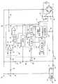
도 1은 본 발명에 따른 전원 제어기의 일 실시예를 갖는 전원 시스템의 일 실시예의 일부를 개략적으로 도시하는 도면.1 shows schematically a part of one embodiment of a power supply system with one embodiment of a power controller according to the invention;

도 2는 본 발명에 따라 도 1의 전원 제어기의 대안적 실시예를 갖는 또 다른 전원 시스템의 일 실시예의 일부를 개략적으로 도시하는 도면.2 is a schematic illustration of a portion of one embodiment of another power supply system with an alternative embodiment of the power controller of FIG. 1 in accordance with the present invention;

도 3은 본 발명에 따른 전원 제어기를 내장한 반도체 디바이스의 일 실시예에 대해 확대된 평면도를 개략적으로 도시하는 도면.3 schematically illustrates an enlarged plan view of an embodiment of a semiconductor device incorporating a power controller according to the present invention;

도면의 간결성과 명료성을 위해, 도면의 구성요소들은 스케일 할 필요성이 없으며, 다른 도면에서 동일한 참조 부호들은 동일한 구성요소들임을 나타낸다. 또한, 잘 알려진 스텝들과 구성요소들의 기재들 및 상세들은 기재의 간결성을 위해 생략한다.For the sake of brevity and clarity of the drawings, the components of the drawings need not be scaled, and like reference numerals in different drawings indicate that the same components. In addition, descriptions and details of well-known steps and components are omitted for brevity of the description.

도 1은 시스템(10)의 출력 전압을 조정하고 제어기(40)와 시스템(10) 양측의 손상을 방지하기 위해 시스템(10)에 대한 입력 전력을 사용하는 전원 제어기(40)의 실시예를 포함하는 전원 시스템(10)의 일 실시예의 일부를 개략적으로 도시한다. 다른 구성요소들은 일반적으로 시스템(10)에 대해 기능성을 제공하기 위해 외부에서 제어기(40)에 접속된다. 예를 들어, 가정용 본선과 같이 AC 전원으로부터 전압 원을 받는 브리지 정류기(11), 에너지 저장 커패시터(17 및 70)와 직렬로 접속되고 정류기(11)와 교차하여 결합된 레지스터들(14 및 15)을 포함하는 분압기, 트랜스포머(18), 블로킹 다이오드(19), 출력 저장 커패시터(21), 출력 트랜지스터 또는 스위치 트랜지스터(26), 피드백 네트워크(29), 및 전류 센스 레지스터(27)가 일반적으로 제어기(40)에 외부적으로 접속된다. 정류기(11)는 실질적으로 dc 파형으로 커패시터(70)에 의해 일반적으로 필터링되는 정류기(11)의 접속점들(12, 13) 사이에서 벌크 전압을 형성한다. 레지스터들(14 및 15)은 접속점들(12 및 13) 사이에서 형성된 벌크전압을 제어기(40)에 의해 사용될 수 있는 입력전압으로 나눈다. 입력단(41)상에 수신된 입력전압은 일반적으로 시스템(10)에 대한 벌크 입력전압을 나타낸다. 제어기(40)는 입력 전압을 수신하고 제어기(40)에 의해 수행된 제어 기능을 위해 사용한다. 레지스터들(14 및 15)의 값은 일반적으로 원하는 기능을 제공하기 위해 선택되고 후술하는 바와 같이 브라운-아웃 검출(brown-out detection)을 위한 전압 레벨로 세트하기 위해 선택될 수도 있다. 제어기(40)는 인가 입력(50)과 전압 복귀(42) 사이의 인가 전압으로서 벌크 입력 전압을 수신하고, 시스템(10)은 출력들(22 및 23) 사이의 출력 전압을 제공한다. 제어기(40)는 제어기(40)에 대한 내부 동작 전압을 제공하기 위해 인가 입력(50)과 복귀(42)를 사용한다. 전형적으로 부하(24)는 출력 전압 외에 시스템(10)으로부터의 부하 전류를 수신하기 위해 출력들(22 및 23) 사이에 접속된다.1 includes an embodiment of apower controller 40 that adjusts the output voltage of thesystem 10 and uses input power to thesystem 10 to prevent damage to both thecontroller 40 and thesystem 10. A schematic diagram of a portion of one embodiment of apower supply system 10 is shown. Other components are generally externally connected to thecontroller 40 to provide functionality for thesystem 10. For example, theresistors 14 and 15 connected in series with therectifier 11 and connected in series with thebridge rectifier 11, theenergy storage capacitors 17 and 70, which receive a voltage source from an AC power source, such as a home mains. A voltage divider, atransformer 18, ablocking diode 19, anoutput storage capacitor 21, an output transistor or aswitch transistor 26, afeedback network 29, and acurrent sense resistor 27 are generally included in the controller ( Is connected externally to 40). Therectifier 11 forms a bulk voltage between thejunctions 12, 13 of therectifier 11, which is generally filtered by thecapacitor 70 in a substantially dc waveform.Registers 14 and 15 divide the bulk voltage formed betweenconnection points 12 and 13 by an input voltage that can be used bycontroller 40. The input voltage received oninput 41 generally represents the bulk input voltage forsystem 10. Thecontroller 40 receives the input voltage and uses it for the control function performed by thecontroller 40. The value of theregisters 14 and 15 is generally selected to provide the desired function and may be selected to set the voltage level for brown-out detection as described below. Thecontroller 40 receives the bulk input voltage as the applied voltage between the appliedinput 50 and thevoltage return 42, and thesystem 10 provides an output voltage between theoutputs 22 and 23.Controller 40 uses anapplication input 50 and return 42 to provide an internal operating voltage forcontroller 40. Typically theload 24 is connected between theoutputs 22 and 23 to receive the load current from thesystem 10 in addition to the output voltage.

전형적으로 트랜지스터(26)는 주 트랜스포머(18)의 한 다리(leg)와 레지스터(27) 사이에 직렬로 접속된 스위칭 전력 트랜지스터이다. 제어기(40)는 드라이브 트랜지스터(26)와 접속된 출력(46)을 갖는다. 전류 센스 레지스터(27)는 노드(28)에서 전류 센스(CS) 신호를 제공하기 위해 트랜지스터(26)와 복귀(42) 사이에 직렬로 접속된다. CS 신호는 트랜지스터(26)를 통해 흐르는 스위치 전류(68)를 나타나는 전압이며, 따라서, 시스템(10)에 대해 입력 전류를 나타낸다. 전류 센스(CS) 신호는 전류 센스(CS) 입력(43) 상의 제어기(40)에 의해 수신된다. 전형적으로 피드백 네트워크(29)는 출력들(22 및 23) 사이의 출력 전압을 나타내는 피드백(FB) 전류(33)를 제공하는 광 커플러이다. 광 커플러는 전형적으로 출력(22)과 기준 접속점(30) 사이에 접속된 발광 다이오드를 갖는다. 기준 전압은 일반적으로 접속점(30)에 인가되어 네트워크(29)의 발광 다이오드에 걸친 전압강하를 더한 기준 전압의 값은 대략 출력들(22 및 23) 사이의 원하는 출력 전압과 동등하다. 예를 들어, 제너 다이오드는 원하는 기준 전압을 제공하기 위해 접속점(30)과 출력(23) 사이에서 접속될 수 있다. 광 커플러는 또한 제어기(40)의 피드백(FB) 입력(44)에 접속된 에미터와 제어기(40)의 전압 단자에 접속된 콜렉터를 갖는 광 트랜지스터를 갖는다. 피드백 네트워크(29)는 또한 직렬 레지스터들을 포함하는 잘 알려진 피드백 회로들 중 하나일 수 있다. 트랜스포머(18), 커패시터(21), 커패시터(70), 다이오드(19), 정류기(11), 및 레지스터들(14 및 15)이 제어기(40)의 동작을 설명하는 것을 돕기 위해 도시된다. 몇몇 실시시예에 있어서, 트랜지스터(26)와 레지스터(27) 중 어느 하나 또는 모두가 제어기(40) 내에 포함될 수 있으나, 가장 바람직한 실시예에 있어서는, 네트워크(29), 트랜지스터(26), 트랜스포머(18), 커패시터(21) 및 다이오드(19)는 제어기(40)가 형성된 반도체 다이 외부에 있다.Transistor 26 is typically a switching power transistor connected in series between a leg ofmain transformer 18 and aresistor 27. Thecontroller 40 has anoutput 46 connected with thedrive transistor 26.Current sense resistor 27 is connected in series betweentransistor 26 and return 42 to provide a current sense (CS) signal atnode 28. The CS signal is the voltage representing theswitch current 68 flowing through thetransistor 26 and therefore represents the input current to thesystem 10. The current sense (CS) signal is received by thecontroller 40 on the current sense (CS)input 43. Typically thefeedback network 29 is an optocoupler providing a feedback (FB) current 33 representing the output voltage between theoutputs 22 and 23. The optocoupler typically has a light emitting diode connected between theoutput 22 and the reference junction 30. The reference voltage is generally applied to the junction 30 so that the value of the reference voltage plus the voltage drop across the light emitting diodes of thenetwork 29 is approximately equal to the desired output voltage between theoutputs 22 and 23. For example, a zener diode can be connected between the junction 30 and theoutput 23 to provide a desired reference voltage. The optocoupler also has a phototransistor with an emitter connected to the feedback (FB)input 44 of thecontroller 40 and a collector connected to the voltage terminal of thecontroller 40.Feedback network 29 may also be one of the well known feedback circuits including serial registers.Transformer 18,capacitor 21,capacitor 70,diode 19,rectifier 11, andresistors 14 and 15 are shown to help explain the operation ofcontroller 40. In some embodiments, either or both of thetransistor 26 and theresistor 27 may be included in thecontroller 40, but in the most preferred embodiment, thenetwork 29, thetransistor 26, the transformer ( 18, thecapacitor 21 and thediode 19 are outside the semiconductor die in which thecontroller 40 is formed.

제어기(40)는 펄스 폭 변조(PWM) 제어기 또는 PWM(61), 기준 발생기 또는 기준(47), 내부 레귤레이터(45), 승산기(51), 및 에러 승산기(52)와 전류 센스(CS) 비교기(56)를 포함하는 에러 블록을 포함한다. 제어기(40)는 전형적으로 드라이버(66)를 포함하며 또한 브라운-아웃 검출기(48)와 같은 그리고 전압저하 로크아웃(under-voltage lock-out; UVLO), 리딩 에지 블랭킹(leading edge blanking), 소프트-스타트(soft-start), 과전압 방지와 같은 도시하지 않은 알려진 또 다른 회로소자와 같은 제어기(40)에 부가적 기능성을 제공하는 또 다른 회로를 포함할 수 있다. 레귤레이터(45)는 인가 입력(50)으로부터 인가 전압을 수신하고 기준(47), 검출기(48), PWM(61), 승산기(51), 증폭기(52) 및 비교기(56)를 포함하는 제어기(40) 내의 구성요소에 대해 내부 동작 전압을 제공한다. 도면의 간결성을 위해 도시하지는 않았지만, 레귤레이터(45)는 입력(50)에 인가된 전압을 수신하기 위해 입력단(50)과 복귀단(42) 사이에 접속된다. 레귤레이터(45)는 또한 제어기(40)와 제어기(40)의 외부 회로를 위한 내부 동작 전압을 제공하기 위해 전압 단자(16)에 접속된 전압 출력을 갖는다. 기준(47)은 증폭기(52)에 의해 이용되고 그리고 제어기(40) 내 어딘가에서 이용되는 전압 기준 신호 Vref1을 생성한다. PWM(61)은 클럭 발생기 또는 주기속도로 클럭 신호를 제공하는 클럭(62), 리세트 우선 RS/래치(63), 및 검출기(48)와 같은 다른 제어 로직에 근거한 변조된 PWM 드라이브 신호에 전형적으로 사용되는 제어 로직(64)을 포함한다. 바람직한 실시예에 있어서, 증폭기(52)와 비교기(56)는 PWM(61)의 일부로 간주된다. 클럭(62)은 래치(63)를 세트하기 위해 사용되고 트랜지스터(26)를 턴-온 또는 활성화하기 위해 트랜지스터(26)의 게이트에 인가되는 드라이브 펄스의 리딩 에지를 형성하는 주기 클럭 펄스를 출력(60) 상에 제공한다. 트랜지스터를 작동시킴으로써 트랜지스터(26)와 레지스터(27)를 통해 흐르는 전류(68)를 형성하고 부하(24)와 충전 커패시터(21)로의 부하 전류를 형성한다. 래치(63)는 비교기(56)의 출력에 의해 로직 하이(high)로 구동될 드라이브 펄스의 후방 에지를 형성하기 위해 리세트된다.Thecontroller 40 is a pulse width modulation (PWM) controller orPWM 61, a reference generator orreference 47, aninternal regulator 45, amultiplier 51, and an error multiplier 52 and a current sense (CS) comparator. And an error block comprising 56. Thecontroller 40 typically includes adriver 66 and is also the same as the brown-out detector 48 and under-voltage lock-out (UVLO), leading edge blanking, soft Other circuitry that provides additional functionality to thecontroller 40, such as another known circuitry not shown, such as soft-start, overvoltage protection. Theregulator 45 receives the applied voltage from theapplication input 50 and includes a controller comprising areference 47, a detector 48, aPWM 61, amultiplier 51, anamplifier 52 and a comparator 56 ( Provide an internal operating voltage for the components in 40). Although not shown for the sake of brevity, theregulator 45 is connected between theinput terminal 50 and thereturn terminal 42 to receive a voltage applied to theinput 50. Theregulator 45 also has a voltage output connected to thevoltage terminal 16 to provide an internal operating voltage for thecontroller 40 and an external circuit of thecontroller 40.Reference 47 generates a voltage reference signal Vref1 that is used byamplifier 52 and used somewhere withincontroller 40. PWM 61 is typical for modulated PWM drive signals based on other control logic such asclock 62, reset priority RS /latch 63, and detector 48, which provide clock signals at a clock generator or periodic rate.Control logic 64 to be used. In the preferred embodiment, theamplifier 52 and thecomparator 56 are considered part of thePWM 61.Clock 62 outputs a periodic clock pulse that is used to setlatch 63 and forms a leading edge of a drive pulse applied to the gate oftransistor 26 to turn on or activate transistor 26 (60). Provide on. Operating the transistor forms a current 68 flowing through thetransistor 26 andresistor 27 and forms a load current to theload 24 and thecharging capacitor 21. Thelatch 63 is reset to form the rear edge of the drive pulse to be driven logic high by the output of thecomparator 56.

제어기(40)는 시스템(10)에 대한 입력 전력의 순시값(instantaneous value)을 계산하기 위한 입력(41)상의 입력 전압과 입력단(43)상의 CS 신호를 사용하기 위해 형성되고, 원하는 동작 값에 대한 출력상의 출력 전압 값을 조정하기 위한 FB 신호와 시스템 입력 전력의 평균 값을 사용하기 위해 형성된다. 예를 들어, 원하는 정규 동작 값이 3.5 볼트라면, 제어기(40)는 대략 3.5볼트까지 출력 전압을 조정하기 위해 입력 전력을 사용한다. 일반적으로 출력 전압 값은 원하는 값의 ±10% 내로 조정된다. 후술하는 바와 같이, 제어기(40)는 PWM(61)에 의해 형성되고 드라이브 트랜지스터(26)에 사용되는 드라이브 펄스의 듀티 사이클을 돕기 위해 입력 전력을 사용한다. 클럭(62)으로부터의 클럭 에지가 래치(63)를 세트할 때, 제어기(40)는 트랜지스터(26)를 작동시키고 전류(68)는 트랜지스터(26)와 레지스터(27) 양측을 통해 흐르고 CS신호를 형성한다. 승산기(51)는 입력 전압과 CS 신호를 수신하고 이에 응답하여 시스템에 대한 순시 입력 전력을 나타내는 전류로서 전력 센스 신호를 형성하기 위해 두 개의 신호를 함께 승산한다. 피드백 네트워크(29)는 FB 전류(33)를 생성한다. 전류들(33 및 67)은 레지스터(31)와 커패시터(32)에 의해 전력 FB 제어 전압으로 변환되는 전력 FB 제어 전류(34)를 형성하기 위해 노드(55)에 서 함께 더해진다. 레지스터(31)를 통과한 전력 FB 제어 전압은 원하는 출력 전압과 실제 출력 전압과의 차이를 나타내는 분량에 더해진 입력 전력을 나타내는 신호의 합을 나타낸다. 전력 FB 제어 전압은 응답하여 출력(59)상에 에러 신호를 생성하는 에러 증폭기(52)에 의해 수신된다. 결과적으로, 에러 신호의 값은 또한 출력 전압을 실질적으로 일정하게 유지하기 위해 요구되는 입력 전력의 총량을 나타낸다. 레지스터들(53 및 54)은 증폭기(52)의 이득을 세트하기 위해 사용된다. 비교기(56)는 에러 전압과 CS 신호를 수신하고 이에 응답하여 래치(63)를 리세트하는 위치에서 전류의 적절한 값을 결정하기 위해 에러 신호에 대해 CS 신호를 비교한다. 래치(63)를 리세트함으로써 트랜지스터(26)에 대한 전류 드라이브 펄스를 종결한다. 이후로 시스템(10)은 삼각파형을 갖는 불연속 전류 동작으로 전형적으로 언급되는 모드로 동작할 것이라는 것을 당업자는 인식할 것이다. 다른 실시예에서 시스템(10)은 사다리꼴 파형을 갖는 연속 전류 모드로 전형적으로 언급되는 모드로 동작한다. 불연속 및 연속 전류 동작 모드는 당업자에게 잘 알려져 있다. 레지스터(31)와 커패시터(32)의 필터는 전류에 의해 나타낸 전력 평균값을 제공하기 위해 전류(67)의 삼각 파형을 통합한다. 필터는 또한 전류(33)에 의해 나타낸 전압 평균값을 제공하기 위해 전류내의 순시적 변화를 통합한다. 필터의 시간 상수는 전형적으로 10 내지 100 (10-100)마이크로 세컨드 범위이다.Thecontroller 40 is configured to use an input voltage on theinput 41 and a CS signal on theinput 43 to calculate an instantaneous value of the input power for thesystem 10 and to a desired operating value. It is formed to use the average value of the FB signal and the system input power to adjust the output voltage value on the output. For example, if the desired normal operating value is 3.5 volts,controller 40 uses the input power to regulate the output voltage to approximately 3.5 volts. Typically, the output voltage value is adjusted to within ± 10% of the desired value. As discussed below, thecontroller 40 uses the input power to assist the duty cycle of the drive pulses formed by thePWM 61 and used in thedrive transistor 26. When the clock edge fromclock 62sets latch 63,controller 40 activatestransistor 26 and current 68 flows through bothtransistor 26 andresistor 27 and the CS signal. To form.Multiplier 51 receives the input voltage and the CS signal and in response multiplies the two signals together to form a power sense signal as a current representing instantaneous input power to the system.Feedback network 29 generatesFB current 33.Currents 33 and 67 are added together atnode 55 to form a power FB control current 34 which is converted by theresistor 31 andcapacitor 32 into a power FB control voltage. The power FB control voltage passing through theregister 31 represents the sum of the signals representing the input power added to the amount representing the difference between the desired output voltage and the actual output voltage. The power FB control voltage is received by theerror amplifier 52 which in response generates an error signal on theoutput 59. As a result, the value of the error signal also represents the total amount of input power required to keep the output voltage substantially constant.Registers 53 and 54 are used to set the gain ofamplifier 52.Comparator 56 compares the CS signal against the error signal to determine the appropriate value of the current at the location that receives the error voltage and the CS signal and in response resets latch 63. The reset of thelatch 63 terminates the current drive pulse for thetransistor 26. Those skilled in the art will then recognize thatsystem 10 will operate in the mode typically referred to as discrete current operation with triangular waveforms. In another embodiment,system 10 operates in a mode typically referred to as a continuous current mode with a trapezoidal waveform. Discontinuous and continuous current operating modes are well known to those skilled in the art. The filter ofresistor 31 andcapacitor 32 incorporate a triangular waveform of current 67 to provide an average value of power represented by the current. The filter also incorporates instantaneous changes in the current to provide the voltage average value represented by current 33. The time constant of the filter is typically in the range of 10 to 100 (10-100) microseconds.

부하(24)가 부하 전류 내의 증가를 요구할 때, 출력들(22 및 23) 사이의 출력 전압은 감소되고 전류(33) 내에서 상응하는 감소를 야기한다. 출력 전압의 변화는 원하는 정상 상태 입력 전압 값 또는 제 1 값의 조건으로부터 또 다른 정상상태 조정 전압 조건으로의 변이를 나타낸다. 입력단(44)에서 전력 FB 제어 전압은 출력 전압이 제 1 값일 때, 제 1 정상상태 값 또는 제 1 값이고, 전류(33)가 변화할 때, 전력 FB 제어 전압이 변화하지만, 이러한 변화는 매우 작다는 것을 주목해야 한다. 이러한 하나의 정상상태 조건으로부터 또 다른 정상상태 조건으로의 변이를 완성시킨다는 것은 완성하는데 몇몇 사이클을 요구한다는 것을 당업자는 이해할 수 있다. 하기에서 기재의 명료성을 위해 사이클의 수는 생략한다. 레지스터(31)와 커패시터(32)의 필터는 전력 FB 제어 전압을 제 1 값으로부터 제 2 값으로 감소시키기 위해 증폭기(52)에 인가됨으로써 야기되는 전압 내의 변화 평균값을 형성하기 위해 전류(33)내의 변화를 통합한다. 감소된 전력 FB 제어 전압의 제 2 값은 증폭기(52)에 의해 수신된다. 증폭기(52)는 인버팅되기 때문에, 출력(59)상의 전압은 제 1 전압으로부터 제 2 전압으로 증가된다. 증폭기(52)는 높은 이득을 갖기 때문에, 증폭기(52)에 의해 수신된 전압 값 내에서의 작은 변화는 출력(59)상의 전압에서의 큰 변화와 전류(68)내 상응하는 큰 변화를 초래한다. 바람직한 실시예에 있어서, 증폭기(52)는 대략 10 정도의 이득을 갖는다. 클럭(62)이 래치(63)를 세트할 때, 입력단(43)에서의 상응하는 전류 센스 신호는 증폭기(51)와 비교기(56)에 의해 수신된다. 상술한 바와 같이, 이러한 변화의 몇몇 사이클은 안정한 정상 상태 조건들 사이에서의 변이를 완성하기 위해 요구된다. 출력(59)의 증가된 제 2 전압 값은 비교기(56)의 출력이 래치(63)를 리세트시키기 위해 하이로 가기 전에 값을 증가시키기 위한 전류(68)와 CS 신호를 요구한다. 전류(68)의 증가된 값은 제 1 정상상태 값에 가까워진 제 2 정상상태 값으로 출력 전압을 이동시킨다. 전류(68) 값과 CS 신호가 증가함에 따라, 전류(67) 값 또한 증가한다. 전력 FB 제어 전압에 대한 제 2 정상상태 값을 형성하기 위해 전류(67) 증가와 전류(33) 감소가 더해진다. 결과적으로, 전류(33 및 67) 총합은 출력으로 이동되는 입력 전력의 총계를 제어하는 동안 원하는 출력 전압 값으로 출력 전압을 조정한다. 상술한 바와 같이, 제어기(40)는 전형적으로 원하는 출력 전압 값의 ±10% 내에서 실질적으로 일정한 값으로 출력 전압을 조정한다. 결과적으로, 입력단(44)상의 전압은 또한 Vref1 값의 ±10% 내에서 실질적으로 일정한 값으로 조정된다. 전류(68) 내 증가는 부하(24)로 요구되는 증가된 부하 전류를 제공하기 위해 그리고 출력 전압의 조정을 유지하기 위해 원하는 출력전압으로 충전된 커패시터(21)를 유지하기 위해 부하 전류를 증가시킨다.When theload 24 requires an increase in the load current, the output voltage between theoutputs 22 and 23 is reduced and causes a corresponding decrease in the current 33. The change in output voltage represents a transition from the desired steady state input voltage value or the condition of the first value to another steady state regulated voltage condition. The power FB control voltage at theinput stage 44 is the first steady state value or the first value when the output voltage is the first value, and the power FB control voltage changes when the current 33 changes, but this change is very significant. It should be noted that it is small. It will be appreciated by those skilled in the art that completing a transition from one steady state condition to another steady state condition requires several cycles to complete. In the following, the number of cycles is omitted for clarity of description. The filter of theresistor 31 and thecapacitor 32 is applied in the current 33 to form an average value of the change in voltage caused by being applied to theamplifier 52 to reduce the power FB control voltage from the first value to the second value. Integrate change. The second value of the reduced power FB control voltage is received by theamplifier 52. Since theamplifier 52 is inverted, the voltage on theoutput 59 is increased from the first voltage to the second voltage. Since theamplifier 52 has a high gain, a small change in the voltage value received by theamplifier 52 results in a large change in the voltage on theoutput 59 and a corresponding large change in the current 68. . In a preferred embodiment, theamplifier 52 has a gain of about 10 degrees. Whenclock 62 sets latch 63, the corresponding current sense signal atinput 43 is received byamplifier 51 andcomparator 56. As mentioned above, several cycles of this change are required to complete the transition between stable steady state conditions. The increased second voltage value of theoutput 59 requires a CS signal and a current 68 to increase the value before the output of thecomparator 56 goes high to reset thelatch 63. The increased value of current 68 shifts the output voltage to a second steady state value approaching the first steady state value. As the current 68 value and the CS signal increase, the current 67 value also increases. Increasing current 67 and decreasing current 33 are added to form a second steady state value for the power FB control voltage. As a result, the sum of thecurrents 33 and 67 adjusts the output voltage to the desired output voltage value while controlling the total amount of input power being delivered to the output. As noted above, thecontroller 40 typically adjusts the output voltage to a substantially constant value within ± 10% of the desired output voltage value. As a result, the voltage on theinput stage 44 is also adjusted to a substantially constant value within ± 10% of the Vref1 value. The increase in current 68 increases the load current to provide the increased load current required by theload 24 and to maintain thecapacitor 21 charged to the desired output voltage to maintain regulation of the output voltage. .

상술한 바와 같이, 전류(68)는 전형적으로 삼각 또는 램프(ramp) 형태를 갖기 때문에, 전류(67) 또한 램프 형태를 갖는다. 레지스터(31)와 커패시터(32)의 필터는 입력 전력 평균 값을 나타내는 전압을 제공하기 위해 전류를 통합한다. 레지스터들(27 및 31)의 값은 시스템(10)에 대한 최대 입력 전력을 세트하기 위해 선택된다. 레지스터(57)와 커패시터(58)는 선택적이고 동작을 향상시키기 위해 승산기(51)에 대한 입력을 분리하는 것을 돕는다. 또한 레지스터(57)와 커패시터(58)는 전류(68) 펄스의 부가적 통합을 제공한다.As noted above, current 68 is typically in the form of a triangular or ramp, so current 67 is also in the form of a lamp. The filter ofresistor 31 andcapacitor 32 incorporates current to provide a voltage representing the average value of the input power. The value of theregisters 27 and 31 is selected to set the maximum input power for thesystem 10.Resistor 57 andcapacitor 58 are optional and help to isolate the input tomultiplier 51 to improve operation. In addition,resistor 57 andcapacitor 58 provide additional integration of the current 68 pulse.

부하 전류에 있어서의 감소를 위해, 동일한 동작이 일어나지만 반대의 극성을 갖는다. 부하 전류에 있어서의 증가에 대한 기재와 같이, 하나의 안정한 조정된 상태로부터 또 다른 안정한 조정된 상태로의 변이는 몇몇 사이클이 발생하지만, 기재의 명확성을 위해 사이클의 수의 설명은 생략한다. 출력 전압과 전류(33)는 증가 하고 증폭기(52)의 출력을 감소시킨다. 트랜지스터(26)에 대한 이어지는 드라이브 펄스는 출력(59)의 감소에 의해 좁아지고 상응하는 전류(68)의 펄스가 짧은 지속기간과 낮은 진폭을 갖도록 한다. 전류(67)는 감소하고 전력 FB 제어 전압에 대한 제 2 정상 상태 값을 형성하기 위해 그리고 출력으로 이동된 입력 전력의 총합을 제어하기 위해 전류(33) 내의 증가와 더해진다.For the reduction in the load current, the same operation takes place but with the opposite polarity. As with the description of the increase in load current, the transition from one stable adjusted state to another stable adjusted state occurs several cycles, but the description of the number of cycles is omitted for clarity of the description. The output voltage and current 33 increase and decrease the output ofamplifier 52. Subsequent drive pulses fortransistor 26 are narrowed by the reduction ofoutput 59 and cause the pulse of corresponding current 68 to have a short duration and low amplitude. Current 67 decreases and adds to the increase in current 33 to form a second steady state value for the power FB control voltage and to control the sum of the input power transferred to the output.

부하(24)에 의해 요구되는 전압과 전류가 일정하게 유지되는 동안 접속점들(12 및 13) 사이에 형성된 벌크 전압이 변화한다면 동일한 형태의 조정이 일어난다. 벌크 전압이 감소 또는 증가한다면, 전류(67)는 각각 감소 또는 증가하고 각각 감소하거나 증가하는 전류(34)를 형성하기 위해 전류(33)에 더해진다. 상술한 바와 같이 출력 전압을 조정하기 위해 제어기(40)는 응답하여 전류를 변화시킨다.The same type of adjustment takes place if the bulk voltage formed between the connection points 12 and 13 changes while the voltage and current required by theload 24 remain constant. If the bulk voltage decreases or increases, current 67 is added to current 33 to form a current 34 that decreases or increases and respectively decreases or increases. As described above, thecontroller 40 responds to the current to adjust the output voltage.

출력들(22 및 23)상의 과부하 조건의 경우에 있어서, 전류(33)는 거의 제로로 감소된다. 출력(59)의 값의 결과는 CS 신호가 출력(59)상의 값과 동등할 때까지 전류(68)의 다음 펄스를 보다 긴 지속시간과 진폭을 갖도록 하는 것을 상당하게 증대시킨다. CS 신호에 있어서의 증가는 커패시터(32)의 충전을 유지하기 위해 그리고 출력(59) 값이 실질적으로 일정하게 유지하는 이전 값으로 출력(59)을 되돌리기 위한 전류(33)내의 감소와 더해지는 전류(67) 값을 증가시킨다. 전류(68)내 증가에 의해 공급된 에너지 총량은 출력 전압의 조정을 유지하기에 충분하지 않으며 출력 전압 값은 감소된다. 하지만, 부하(24)로 공급된 전력, 입력 전력은 출력들(22 및 23) 사이가 단락된다 하더라도 실질적으로 일정하게 유지된다. 전력을 일정하게 유지한다는 것은 제어기(40)와 다른 시스템(10)의 구성요소의 손상을 방지한다는 것 이다. 출력들(22 및 23) 사이가 개방 회로인 경우에 있어, 반대 현상이 발생, 즉 전류(33)는 증가하고 전류(67)는 실질적으로 제로로 간다. 제어기(40)는 입력단(44)에서 전압 값의 증가를 수신하고 실질적으로 일정하게 출력 전압을 유지하기 위해 입력 전력을 사용한다.In the case of an overload condition on theoutputs 22 and 23, the current 33 is reduced to almost zero. The result of the value of theoutput 59 significantly increases that the next pulse of the current 68 has a longer duration and amplitude until the CS signal is equivalent to the value on theoutput 59. The increase in the CS signal results in a decrease in current 33 and added current to maintain charging ofcapacitor 32 and to returnoutput 59 to a previous value at whichoutput 59 value remains substantially constant. 67) Increase the value. The total amount of energy supplied by the increase in current 68 is not sufficient to maintain the adjustment of the output voltage and the output voltage value is reduced. However, the power supplied to theload 24, the input power, remains substantially constant even if theoutputs 22 and 23 are shorted. Keeping the power constant is to prevent damage to thecontroller 40 and other components of thesystem 10. In the case of an open circuit between theoutputs 22 and 23, the opposite occurs, i.e. the current 33 increases and the current 67 goes substantially zero.Controller 40 uses input power to receive an increase in voltage value atinput 44 and maintain the output voltage substantially constant.

본 동작을 용이하게 하기 위해, 레귤레이터(45)의 전압 입력은 입력단(50)에 접속되고 레귤레이터(45)의 전압복귀는 복귀단(42)에 접속된다. 기준(47)의 Vref1 출력은 증폭기(52)의 비-인버팅 입력에 접속된다. 증폭기(52)의 인버팅 입력은 통상적으로 레지스터(53)의 제 1 단자와 레지스터(54)의 제 1 단자에 접속된다. 레지스터(53)의 제 2 단자는 증폭기(52)의 출력에 접속되고 비교기(56)의 비-인버팅 입력에 접속된다. 비교기(56)의 인버팅 입력은 입력단(43)에 접속되고 레지스터(57)의 제 1 단자에 접속되며, 비교기(56)의 출력은 래치(63)의 리세트 입력에 접속된다. 래치(63)의 출력은 로직(64)의 입력에 접속된다. 래치(63)의 세트 입력은 클럭(62)의 출력에 접속된다. 로직(64)의 출력은 드라이버(66)의 입력에 접속된다. 출력 드라이버(66)는 출력단(46)에 접속된다. 증폭기(51)의 제 1 입력은 입력단(41)에 접속되고 증폭기(51)의 제 2 입력은 통상적으로 레지스터(57)의 제 2 단자와 커패시터(58)의 제 1 단자에 접속된다. 커패시터(58)의 제 2 단자는 복귀단(42)에 접속된다. 증폭기(51)의 출력은 통상적으로 레지스터(54)의 제 2 단자에 접속되고 입력단(44)에 접속된다.To facilitate this operation, the voltage input of theregulator 45 is connected to theinput terminal 50 and the voltage return of theregulator 45 is connected to thereturn terminal 42. The Vref1 output ofreference 47 is connected to the non-inverting input ofamplifier 52. The inverting input of theamplifier 52 is typically connected to the first terminal of theregister 53 and the first terminal of theresistor 54. The second terminal of theresistor 53 is connected to the output of theamplifier 52 and to the non-inverting input of thecomparator 56. The inverting input ofcomparator 56 is connected to input 43 and is connected to the first terminal ofregister 57, and the output ofcomparator 56 is connected to the reset input oflatch 63. The output oflatch 63 is connected to the input oflogic 64. The set input of thelatch 63 is connected to the output of theclock 62. The output oflogic 64 is connected to the input ofdriver 66. Theoutput driver 66 is connected to theoutput terminal 46. The first input of theamplifier 51 is connected to theinput terminal 41 and the second input of theamplifier 51 is typically connected to the second terminal of theresistor 57 and the first terminal of thecapacitor 58. The second terminal of thecapacitor 58 is connected to thereturn end 42. The output of theamplifier 51 is typically connected to the second terminal of theresistor 54 and to theinput terminal 44.

도 2에는 도 1에서 도시된 제어기(40)의 대안적 실시예인 전원 제어기(91)를 포함하는 전원 시스템(90)의 실시예의 일부를 개략적으로 도시한다. 시스템(90)은 부스트 컨버터(boost converter)로서 구성되고 FB 전류(33)와 상응하는 피드백 전압을 공급하기 위해 접속된 입력 인덕터(36), 블로킹 다이오드(37), 및 레지스터들(38 및 39)을 포함한다. 제어기(91)와 시스템(90)의 동작은 시스템(10)에 대해 기재된 것과 유사하다. 하지만, 시스템(90)은 연속 전도 모드로 동작한다. 접속점들(12 및 13) 사이의 벌크 전압은 필터링되지 않고 따라서, 벌크 전압은 해버사인 파형(haversine waveform)을 갖는다. 전류(68)는 트랜지스터(26)의 활성화와 비활성화에 의해 형성된 램프 파형으로 변조된 해버사인 포락선을 갖는 파형을 갖는다. 결과적으로, 전류(67)는 전류(68)와 같이 동일한 파 형상인 파형을 갖는다. 이는 연속 전도 모드이기 때문에, 램프 파형은 해버사인 파형의 상단에서 오른다. 또한 본 실시예에서 주목할 것은, 클럭(62)이 부가적인 램프 출력(65)을 가지며 그 발생기(74)는 출력 Vref2 상에 부가적인 전압 기준 신호 Vref2를 갖는다는 것이다.2 schematically illustrates a portion of an embodiment of apower supply system 90 that includes apower supply controller 91, which is an alternative embodiment of thecontroller 40 shown in FIG. 1. Thesystem 90 is configured as a boost converter and is connected with aninput inductor 36, blockingdiode 37, andresistors 38 and 39 to supply a feedback voltage corresponding to the FB current 33. It includes. The operation ofcontroller 91 andsystem 90 is similar to that described forsystem 10. However,system 90 operates in continuous conduction mode. The bulk voltage between the connection points 12 and 13 is not filtered and therefore the bulk voltage has a haberine waveform.Current 68 has a waveform with a heber sine envelope modulated with a ramp waveform formed by activation and deactivation oftransistor 26. As a result, the current 67 has a waveform having the same wave shape as the current 68. Since this is a continuous conduction mode, the ramp waveform rises on top of the hebersignal waveform. Also note in this embodiment thatclock 62 has anadditional ramp output 65 and itsgenerator 74 has an additional voltage reference signal Vref2 on output Vref2.

제어기(91)는 증폭기(52), 제산기(94), 가산기(92), 및 비교기(93)를 갖는 에러 블럭(95)을 포함한다. 입력단(44)상에 수신된 전력 FB 제어 전압, 즉 증폭기(52)의 출력은 출력 전압을 나타내고 출력 전압의 증가 또는 감소를 따른다. 제산기(94)는 출력 전압내의 변화를 필요로 하는 입력 전력의 변화를 나타내는 신호를 형성하기 위해 출력 전압에 의해 입력 전력을 나눈다. 출력 전압이 감소하면, 예를 들어, 부하 전류에 있어서의 증가의 결과로서, 입력단(44)상의 전압이 감소하고, 따라서, 제산기(94)의 출력이 증가된 입력 전력의 필요성을 나타내는 것을 감소시킨다. 결과적으로, 출력 전압 내의 증가는 제산기(94)의 출력에 있어서의 증가라는 결과가 된다. 가산기(92)는 트랜지스터(26)의 듀티 사이클을 변조하기 위해 제산기 (94)의 출력에 클럭(62)으로부터의 램프를 더한다. 비교기(93)는 트랜지스터(26)가 스위치할 출력단에서 가산기의 전압 레벨을 세트하기 위해 가산기(92)의 출력을 기준 전압 Vref2와 비교한다.Thecontroller 91 includes anerror block 95 with anamplifier 52, adivider 94, anadder 92, and a comparator 93. The power FB control voltage received oninput 44, i.e., the output ofamplifier 52, represents the output voltage and follows the increase or decrease of the output voltage.Divider 94 divides the input power by the output voltage to form a signal indicative of a change in input power that requires a change in the output voltage. If the output voltage decreases, for example, as a result of an increase in load current, the voltage oninput stage 44 decreases, thus reducing the output ofdivider 94 indicating the need for increased input power. Let's do it. As a result, the increase in the output voltage results in an increase in the output of thedivider 94.Adder 92 adds a ramp fromclock 62 to the output ofdivider 94 to modulate the duty cycle oftransistor 26. Comparator 93 compares the output ofadder 92 with reference voltage Vref2 to set the voltage level of the adder at the output stage thattransistor 26 will switch.

도 3은 반도체 다이(96)가 형성된 반도체 디바이스(97)의 실시예의 일부에 대한 확장된 평면도를 개략적으로 도시한다. 제어기(40)는 다이(96)상에 형성된다. 다이(96)는 도면의 간략성을 위해 도 3에 도시하지 않은 다른 회로를 포함할 수 있다. 제어기(40)와 디바이스(97)는 당업자에게 알려진 반도체 제조 기술들에 의해 다이(96)상에 형성된다.3 schematically illustrates an expanded plan view of a portion of an embodiment of asemiconductor device 97 in which asemiconductor die 96 is formed.Controller 40 is formed ondie 96.Die 96 may include other circuitry not shown in FIG. 3 for simplicity of the drawing.Controller 40 anddevice 97 are formed on die 96 by semiconductor fabrication techniques known to those skilled in the art.

상술한 모든 관점에서, 신규한 디바이스와 방법이 개시된 것은 명백하다. 다른 특징들 속에 포함된 것은, 출력 전압 값을 원하는 출력 전압 값으로 조정하기 위해 입력 전력 값을 사용한다는 것이다. 출력 전압을 조정하기 위해 입력 전력 값을 사용함으로써 벌크 입력 전압 내의 변화의 검출과 실질적으로 일정한 출력 전압을 유지하기 위해 듀티 사이클을 변화시키는 것이 용이하게 된다. 부가적으로, 입력 전력을 사용하여 과부하 조건 동안 실질적으로 일정한 입력 전력을 유지하는 것을 용이하게 함으로써 손상으로부터 시스템 및 제어기(40)를 보호할 수 있다. 피드백 전류와 승산기 전류 값을 더함으로써 전원 제어기에 대한 피드백 신호를 형성하기 위한 반도체 패키지의 단일 핀 사용을 용이하게 한다. 입력 전압과 브라운-아웃 검출 양측에 대해 입력 전압을 사용함으로써 또한 반도체 패키지에서 사용되는 핀들의 수를 줄인다.In view of all the above, it is apparent that the novel devices and methods are disclosed. Included in other features is the use of input power values to adjust the output voltage value to the desired output voltage value. Using the input power value to adjust the output voltage facilitates detection of changes in the bulk input voltage and varying duty cycle to maintain a substantially constant output voltage. Additionally, the input power can be used to protect the system andcontroller 40 from damage by facilitating maintaining a substantially constant input power during overload conditions. Adding the feedback current and the multiplier current values facilitates the use of a single pin of the semiconductor package to form a feedback signal to the power controller. Using input voltages for both input voltage and brown-out detection also reduces the number of pins used in semiconductor packages.

본 발명이 바람직한 실시예와 함께 기재되어 왔지만, 다양한 대안들 및 변경 들이 반도체 업계의 당업자가 명백하다는 것이 명확하다. 예를 들어, 승산기(51)는 전압 입력 대신에 전류 입력을 갖도록 형성될 수 있으며, 승산기(51)의 출력은 전류 대신에 전압일 수 있다. 또한, 승산기(51)는 당업자에 의해 알려진 다양한 구현예들로부터 형성될 수 있다.Although the present invention has been described with preferred embodiments, it is clear that various alternatives and modifications will be apparent to those skilled in the semiconductor arts. For example,multiplier 51 may be configured to have a current input instead of a voltage input, and the output ofmultiplier 51 may be a voltage instead of a current.Multiplier 51 may also be formed from various embodiments known by those skilled in the art.

Claims (20)

Translated fromKorean
전원 시스템의 동작 방법에 있어서,In the operation method of the power system,상기 전원 시스템의 입력 전력을 계산하는 단계; 및Calculating an input power of the power system; And원하는 값으로 상기 전원 시스템의 출력 전압을 조정하기 위해 상기 입력 전력을 사용하는 단계를 포함하는, 전원 시스템 동작 방법.Using the input power to adjust the output voltage of the power system to a desired value.제 1 항에 있어서, 상기 출력 전압을 조정하기 위해 상기 입력 전력을 사용하는 단계는, 상기 전원 시스템의 전력 스위치에 대한 드라이브 펄스들을 변조하기 위해 상기 입력 전력을 사용하는 단계를 포함하는, 전원 시스템 동작 방법.2. The power system operation of claim 1, wherein using the input power to adjust the output voltage comprises using the input power to modulate drive pulses for a power switch of the power system. Way.제 1 항에 있어서, 상기 전원 시스템의 입력 전력을 계산하는 단계는, 상기 입력 전력을 나타내는 전력 신호를 생성하는 단계와 상기 전력 신호와 상기 출력 전압을 나타내는 피드백 신호를 더하는 단계를 포함하는, 전원 시스템 동작 방법.The power supply system of claim 1, wherein calculating the input power of the power supply system comprises generating a power signal indicative of the input power and adding a feedback signal indicative of the power signal and the output voltage. How it works.제 1 항에 있어서, 브라운-아웃 검출(brown-out detection)을 위해 입력 전압을 나타내는 신호를 사용하는 단계를 더 포함하는, 전원 시스템 동작 방법.2. The method of claim 1, further comprising using a signal indicative of an input voltage for brown-out detection.전원 제어기 형성 방법에 있어서,In the method of forming a power controller,입력 전압을 나타내는 제 1 신호와 입력 전류를 나타내는 제 2 신호를 수신 하여 입력 전력을 나타내는 전력 신호를 형성하기 위해 전원 제어기를 결합하는 단계;Coupling a power supply controller to receive a first signal representing an input voltage and a second signal representing an input current to form a power signal representing input power;출력 전압을 나타내는 피드백 신호를 수신하기 위해 상기 전원 제어기를 결합하는 단계; 및Coupling the power controller to receive a feedback signal indicative of an output voltage; And상기 전력 신호와 상기 피드백 신호에 응답하여 상기 출력 전압을 조정하기 위한 드라이브 펄스들을 형성하기 위해 상기 전원 제어기를 결합하는 단계를 포함하는, 전원 제어기 형성 방법.Coupling the power controller to form drive pulses for adjusting the output voltage in response to the power signal and the feedback signal.제 5 항에 있어서, 상기 전력 신호와 상기 피드백 신호에 응답하여 상기 출력 전압을 조정하기 위한 드라이브 펄스들을 형성하기 위해 상기 전원 제어기를 결합하는 단계는, 상기 피드백 신호와 상기 전력 신호를 더하기 위해 상기 전원 제어기를 결합하는 단계를 포함하는, 전원 제어기 형성 방법.6. The method of claim 5, wherein combining the power controller to form drive pulses to adjust the output voltage in response to the power signal and the feedback signal comprises: adding the power supply signal to the power supply signal to add the feedback signal and the power signal; Coupling a controller.제 5 항에 있어서, 상기 입력 전압을 나타내는 제 1 신호와 상기 입력 전류를 나타내는 제 2 신호를 수신하여 상기 전력 신호를 형성하기 위해 전원 제어기를 결합하는 단계는, 상기 제 1 신호와 상기 제 2 신호를 수신하여 상기 전력 신호를 형성하기 위해 승산기를 결합하는 단계를 포함하는, 전원 제어기 형성 방법.6. The method of claim 5, wherein combining a power controller to receive the first signal representing the input voltage and the second signal representing the input current to form the power signal comprises: the first signal and the second signal; Coupling a multiplier to receive a signal to form the power signal.제 5 항에 있어서, 상기 출력 전압을 조정하기 위한 드라이브 펄스들을 형성하기 위해 전원 제어기를 결합하는 단계는, 상기 피드백 신호에 의해 상기 전력 신 호를 나누도록 상기 전원 제어기를 결합하는 단계를 포함하는, 전원 제어기 형성 방법.6. The method of claim 5, wherein combining the power controller to form drive pulses to adjust the output voltage comprises combining the power controller to divide the power signal by the feedback signal. How to form a power controller.제 5 항에 있어서, 상기 전력 신호와 상기 피드백 신호에 응답하여 상기 출력 전압을 조정하기 위한 드라이브 펄스들을 형성하기 위해 상기 전원 제어기를 결합하는 단계는, 전력 피드백 제어 신호를 형성하도록 상기 피드백 신호와 상기 전력 신호를 더하기 위해 상기 전원 제어기를 결합하는 단계를 포함하는, 전원 제어기 형성 방법.6. The method of claim 5, wherein combining the power controller to form drive pulses for adjusting the output voltage in response to the power signal and the feedback signal comprises: forming the power feedback control signal and the feedback signal; Coupling the power controller to add a power signal.제 9 항에 있어서, 상기 피드백 신호와 상기 전력 신호를 더하기 위해 상기 전원 제어기를 결합하는 단계는, 상기 전력 피드백 제어 신호를 수신하여 에러 신호를 형성하기 위해 에러 증폭기를 결합하는 단계를 더 포함하고, 상기 에러 신호와 상기 제 2 신호를 수신하여 상기 드라이브 펄스들의 듀티 사이클을 변조하도록 비교기를 결합하는 단계를 더 포함하는, 전원 제어기 형성 방법.10. The method of claim 9, wherein combining the power controller to add the feedback signal and the power signal further comprises combining an error amplifier to receive the power feedback control signal and form an error signal, Coupling a comparator to receive the error signal and the second signal and modulate the duty cycle of the drive pulses.제 5 항에 있어서, 상기 전력 신호와 상기 피드백 신호에 응답하여 상기 출력 전압을 조정하기 위한 드라이브 펄스들을 형성하기 위해 상기 전원 제어기를 결합하는 단계는, 적어도 원하는 값의 ±10% 이내로 상기 출력 전압을 조정하기 위해 상기 전원 제어기를 결합하는 단계를 포함하는, 전원 제어기 형성 방법.6. The method of claim 5, wherein combining the power controller to form drive pulses for adjusting the output voltage in response to the power signal and the feedback signal, at least within ± 10% of the desired value. Coupling the power controller to adjust.제 5 항에 있어서, 상기 입력 전압을 나타내는 제 1 신호와 상기 입력 전류를 나타내는 제 2 신호를 수신하여 상기 전력 신호를 형성하기 위해 상기 전원 제어기를 결합하는 단계는, 상기 제 1 신호를 수신하기 위해 상기 전원 제어기의 브라운-아웃 검출 회로를 결합하는 단계를 포함하는, 전원 제어기 형성 방법.6. The method of claim 5, wherein combining the power controller to receive the first signal representing the input voltage and the second signal representing the input current to form the power signal comprises: receiving the first signal; Coupling the brown-out detection circuit of the power controller.제 5 항에 있어서, 상기 입력 전압을 나타내는 제 1 신호와 상기 입력 전류를 나타내는 제 2 신호를 수신하여 상기 전력 신호를 형성하기 위해 상기 전원 제어기를 결합하는 단계는, 해버사인 파형(haversine waveform)을 갖는 상기 전력 신호를 응답적으로 형성하기 위해 상기 전원 제어기 신호를 결합하는 단계를 포함하는, 전원 제어기 형성 방법.6. The method of claim 5, wherein the step of combining the power controller to receive the first signal representing the input voltage and the second signal representing the input current to form the power signal comprises: forming a haberine waveform; Combining the power controller signal to responsively form the power signal having a power supply controller.제 5 항에 있어서, 상기 전력 신호와 상기 피드백 신호에 응답하여 상기 출력 전압을 조정하기 위한 드라이브 펄스들을 형성하기 위해 상기 전원 제어기를 결합하는 단계는, 과부하 조건 동안 실질적으로 일정한 입력 전력을 유지하기 위해 전원 제어기를 결합하는 단계를 포함하는, 전원 제어기 형성 방법.6. The method of claim 5, wherein combining the power controller to form drive pulses for regulating the output voltage in response to the power signal and the feedback signal comprises: maintaining a substantially constant input power during an overload condition. Coupling a power controller.전원 제어기에 있어서,In the power controller,입력 전압을 나타내는 전압과 입력 전류를 나타내는 전류 센스 신호를 수신하여 입력 전력을 나타내는 전력 신호를 형성하기 위해 결합된 승산기;A multiplier coupled to receive a voltage representing an input voltage and a current sense signal representing an input current to form a power signal representing input power;출력 전압을 조정하기 위한 드라이브 펄스들을 형성하기 위해 결합된 상기 전원 제어기의 PWM 제어기; 및A PWM controller of the power controller coupled to form drive pulses for adjusting the output voltage; And상기 전력 신호, 피드백 신호, 및 상기 전류 센스 신호를 수신하여, 상기 드라이브 펄스들을 형성하도록 상기 PWM 제어기를 응답적으로 제어하기 위해 결합된 상기 전원 제어기의 에러 블럭을 포함하는, 전원 제어기.And an error block of the power controller coupled to receive the power signal, a feedback signal, and the current sense signal and to responsively control the PWM controller to form the drive pulses.제 15 항에 있어서, 상기 전력 신호, 피드백 신호, 및 상기 전류 센스 신호를 수신하여, 상기 드라이브 펄스들을 형성하기 위해 결합된 상기 전원 제어기의 에러 블럭은 상기 전력 신호와 상기 피드백 신호를 더하기 위해 결합된 상기 전원 제어기의 입력을 포함하는, 전원 제어기.16. The apparatus of claim 15, wherein the error block of the power controller coupled to receive the power signal, the feedback signal, and the current sense signal, to form the drive pulses is coupled to add the power signal and the feedback signal. A power controller comprising an input of the power controller.제 15 항에 있어서, 상기 입력 전압을 나타내는 상기 전압을 수신하기 위해 결합된 브라운-아웃 검출기를 더 포함하는, 전원 제어기.16. The power controller of claim 15, further comprising a brown-out detector coupled to receive the voltage representative of the input voltage.제 15 항에 있어서, 상기 전력 신호, 상기 피드백 신호, 및 상기 전류 센스 신호를 수신하기 위해 결합된 상기 전원 제어기의 에러 블럭은 상기 전력 신호와 상기 피드백 신호를 수신하여 증폭기의 출력상의 전압을 형성하기 위해 결합된 상기 증폭기를 포함하는, 전원 제어기.16. The apparatus of claim 15, wherein an error block of the power controller coupled to receive the power signal, the feedback signal, and the current sense signal receives the power signal and the feedback signal to form a voltage on an output of an amplifier. And said amplifier coupled to.제 18 항에 있어서, 상기 전류 센스 신호 및 상기 증폭기의 출력상의 상기 전압을 수신하고 상기 드라이브 펄스들을 듀티 사이클을 변조하기 위해 결합된 비 교기를 더 포함하는, 전원 제어기.19. The power controller of claim 18, further comprising a comparator coupled to receive the current sense signal and the voltage on the output of the amplifier and modulate the drive pulses on a duty cycle.제 15 항에 있어서, 상기 전력 신호, 상기 피드백 신호, 및 상기 전류 센스 신호를 수신하기 위해 결합된 상기 전원 제어기의 에러 블럭은 상기 피드백 신호를 수신하여 출력을 형성하기 위해 결합된 증폭기를 포함하고, 상기 증폭기의 출력에 의해 상기 전력 신호를 나누기 위해 결합된 제산기를 더 포함하는, 전원 제어기.16. The apparatus of claim 15, wherein the error block of the power controller coupled to receive the power signal, the feedback signal, and the current sense signal comprises an amplifier coupled to receive the feedback signal and form an output, And a divider coupled to divide the power signal by the output of the amplifier.
KR1020057020374A2004-02-262004-02-26 Method and structure of power controllerExpired - LifetimeKR101045196B1 (en)

Priority Applications (1)

Application NumberPriority DateFiling DateTitle
KR1020057020374AKR101045196B1 (en)2004-02-262004-02-26 Method and structure of power controller

Applications Claiming Priority (1)

Application NumberPriority DateFiling DateTitle
KR1020057020374AKR101045196B1 (en)2004-02-262004-02-26 Method and structure of power controller

Publications (2)

Publication NumberPublication Date
KR20060118321Atrue KR20060118321A (en)2006-11-23
KR101045196B1 KR101045196B1 (en)2011-06-30

Family

ID=37705560

Family Applications (1)

Application NumberTitlePriority DateFiling Date
KR1020057020374AExpired - LifetimeKR101045196B1 (en)2004-02-262004-02-26 Method and structure of power controller

Country Status (1)

CountryLink
KR (1)KR101045196B1 (en)

Family Cites Families (1)

* Cited by examiner, † Cited by third party
Publication numberPriority datePublication dateAssigneeTitle
JP4003792B2 (en)*2004-11-172007-11-07オムロン株式会社 Servo motor control system

Also Published As

Publication numberPublication date
KR101045196B1 (en)2011-06-30

Similar Documents

PublicationPublication DateTitle
US7447601B2 (en)Power supply controller method and structure
US7254000B1 (en)Over voltage protection scheme for synchronous buck converter
US6377032B1 (en)Method and apparatus for virtual current sensing in DC-DC switched mode power supplies
US7760520B2 (en)Current controlled switching mode power supply
JP3254199B2 (en) DC-DC converter having inductor current detector and adjustment method thereof
US9253832B2 (en)Power supply circuit with a control terminal for different functional modes of operation
US8085563B2 (en)Protection and clamp circuit for power factor correction controller
US7298124B2 (en)PWM regulator with discontinuous mode and method therefor
US7071667B2 (en)DC—DC converter
US5440473A (en)AC-DC converter
US4293902A (en)Transformerless fast current limiter with symetry correction for a switched-mode power supply
US6011382A (en)Circuit and method for directly regulating the output voltage of an electroluminescent lamp driver
JPH10225105A (en)Dc-dc converter
US20060171179A1 (en)Low audible noise power supply method and controller therefor
US20040012376A1 (en)Current-mode switching regulator
EP1087506A2 (en)Frequency control of switch-mode power supply
US11081957B2 (en)Power converter with multi-mode timing control
JP5032447B2 (en) Switching power supply
JP3196554B2 (en) Current mode switching stabilized power supply
KR101045196B1 (en) Method and structure of power controller
US20230180365A1 (en)A driving circuit, and led circuit and a driving method
JPS60148377A (en) DC/DC converter
JP3006775B2 (en) Switching power supply
JP3227637B2 (en) Power supply circuit
JP3058304B2 (en) Converter overcurrent protection circuit

Legal Events

DateCodeTitleDescription
PA0105International application

Patent event date:20051026

Patent event code:PA01051R01D

Comment text:International Patent Application

PG1501Laying open of application
A201Request for examination
PA0201Request for examination

Patent event code:PA02012R01D

Patent event date:20090219

Comment text:Request for Examination of Application

E902Notification of reason for refusal
PE0902Notice of grounds for rejection

Comment text:Notification of reason for refusal

Patent event date:20101020

Patent event code:PE09021S01D

E701Decision to grant or registration of patent right
PE0701Decision of registration

Patent event code:PE07011S01D

Comment text:Decision to Grant Registration

Patent event date:20110531

GRNTWritten decision to grant
PR0701Registration of establishment

Comment text:Registration of Establishment

Patent event date:20110623

Patent event code:PR07011E01D

PR1002Payment of registration fee

Payment date:20110624

End annual number:3

Start annual number:1

PG1601Publication of registration
FPAYAnnual fee payment

Payment date:20140529

Year of fee payment:4

PR1001Payment of annual fee

Payment date:20140529

Start annual number:4

End annual number:4

FPAYAnnual fee payment

Payment date:20160330

Year of fee payment:6

PR1001Payment of annual fee

Payment date:20160330

Start annual number:6

End annual number:6

FPAYAnnual fee payment

Payment date:20180601

Year of fee payment:8

PR1001Payment of annual fee

Payment date:20180601

Start annual number:8

End annual number:8

PR1001Payment of annual fee

Payment date:20210525

Start annual number:11

End annual number:11

PC1801Expiration of term

Termination date:20240826

Termination category:Expiration of duration


[8]ページ先頭

©2009-2025 Movatter.jp